首页 > HMC407MS8GE > 详情
 Datasheet下载
- 型号: HMC407MS8GE
- 制造商: Hittite
- 库位|库存: xxxx|xxxx
- 要求:
| 数量阶梯 | 香港交货 | 国内含税 |
| +xxxx | $xxxx | ¥xxxx |
查看当月历史价格
查看今年历史价格
产品参数
| 参数 | 数值 |
| 产品目录 | 射频/IF 和 RFID |
| 描述 | POWER AMP 5-6GHZ INGAP 8MSOP |
| 产品分类 | RF 放大器 |
| 品牌 | Hittite Microwave Corporation |
| 数据手册 | 点击此处下载产品Datasheet |
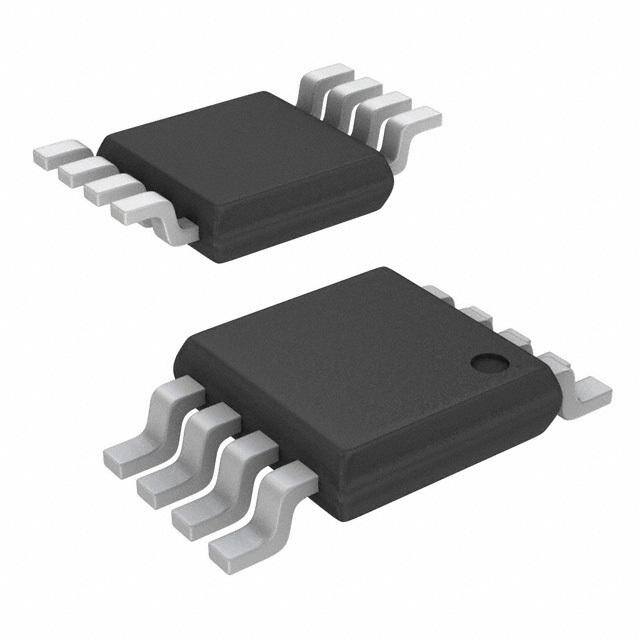
| 产品图片 |  |
| P1dB | 25dBm |
| 产品型号 | HMC407MS8GE |
| RF类型 | 通用 |
| rohs | 无铅 / 符合限制有害物质指令(RoHS)规范要求 |
| 产品系列 | - |
| 供应商器件封装 | 8-MSOP-EP |
| 其它名称 | 1127-1032-1 |
| 包装 | 剪切带 (CT) |
| 噪声系数 | 5.5dB |
| 增益 | 15dB |
| 封装/外壳 | 8-TSSOP,8-MSOP(0.118",3.00mm 宽)裸焊盘 |
| 标准包装 | 1 |
| 测试频率 | - |
| 电压-电源 | 5V |
| 电流-电源 | 230mA |
| 频率 | 5GHz ~ 7GHz |
Datasheet
PDF Datasheet 数据手册内容提取
HMC407MS8G 407MS8GE / v03.1006 GaAs InGaP HBT MMIC POWER AMPLIFIER, 5 - 7 GHz Typical Applications Features This amplifi er is ideal for use as a power Gain: 15 dB amplifi er for 5 - 7 GHz applications: Saturated Power: +29 dBm • UNII 28% PAE • HiperLAN Supply Voltage: +5V 11 Power Down Capability No External Matching Required T M Functional Diagram General Description S The HMC407MS8G & HMC407MS8GE are high - efficiency GaAs InGaP Heterojunction Bipolar S R Transistor (HBT) MMIC Power amplifi ers which E operate between 5 and 7 GHz. The amplifi er requires I no external matching to achieve operation and is F thus truly 50 Ohm matched at input and output. The I L amplifi er is packaged in a low cost, surface mount P 8 leaded package with an exposed base for im- M proved RF and thermal performance. The amplifi er A provides 15 dB of gain, +29 dBm of saturated power R at 28% PAE from a +5V supply voltage. Power down E capability is available to conserve current consum- W ption when the amplifi er is not in use. O P & R Electrical Specifi cations, T = +25° C, Vs = 5V, Vpd = 5V A A E Parameter Min. Typ. Max. Min. Typ. Max. Units N Frequency Range 5 - 7 5.6 - 6.0 GHz I L Gain 10 15 18 12 15 18 dB Gain Variation Over Temperature 0.025 0.035 0.025 0.035 dB/ °C Input Return Loss 12 12 dB Output Return Loss 15 15 dB Output Power for 1 dB Compression (P1dB) 21 25 22 25 dBm Saturated Output Power (Psat) 29 29 dBm Output Third Order Intercept (IP3) 32 37 36 40 dBm Noise Figure 5.5 5.5 dB Supply Current (Icq) Vpd = 0V/5V 0.002 / 230 0.002 / 230 mA Control Current (Ipd) Vpd = 5V 7 7 mA Switching Speed tON, tOFF 30 30 ns Information furnisheFd obry Apnrailcoge D, edviceelsi vise breylie,v eadn tdo bteo a cpcluaractee a nod rrdelieabrlse., Hpowleevaers, eno coFnotra pcritc eH, idtteiltieve rMy, iacnrdo wtoa pvlaec eC oorrdperosr: aAtnioalnog: Devices, Inc., responsibility is assumed by Analog Devices for its use, nor for any infringements of patents or other One Technology Way, P.O. Box 9106, Norwood, MA 02062-9106 11 - 28 rights of third parties th2at 0m aAy rlepsuhlt afro mR iots ausde., S Cpehcifeicalmtionss fsoubrjdec,t tMo cAhan 0ge1 w8it2ho4ut n oPticheo. Nnoe : P9h7o8ne-:2 75801--33239-44370 0F (cid:127)a Oxr:d 9er7 o8n-li2ne5 a0t- w3w3w7.3analog.com license is granted by implication or otherwise under any patent or patent rights of Analog Devices. Trademarks and registered trademarks are the property of their resOpercdtivee orw Onerns.-line at www.hAiptptilticea.tcioonm Support: Phone: 1-800-ANALOG-D
HMC407MS8G / 407MS8GE v03.1006 GaAs InGaP HBT MMIC POWER AMPLIFIER, 5 - 7 GHz Broadband Gain & Return Loss Gain vs. Temperature 20 20 15 10 16 dB) 5 S21 NSE ( 0 SS1212 N (dB) 12 SPO -5 GAI 8 ++2855 CC 11 RE -10 -40 C -15 4 -20 T -25 0 2 3 4 5 6 7 8 9 10 4 4.5 5 5.5 6 6.5 7 7.5 8 M FREQUENCY (GHz) FREQUENCY (GHz) S - S Input Return Loss vs. Temperature Output Return Loss vs. Temperature R E 0 0 I F dB) -5 ++-428055 CCC dB) -5 ++-428055 CCC PLI SS ( SS ( -10 M O O L -10 L N N A ETUR ETUR -15 R R R -15 -20 E W -20 -25 O 4 4.5 5 5.5 6 6.5 7 7.5 8 4 4.5 5 5.5 6 6.5 7 7.5 8 P FREQUENCY (GHz) FREQUENCY (GHz) & R P1dB vs. Temperature Psat vs. Temperature A E 34 34 N 30 30 LI m) 26 m) 26 P1dB (dB 22 Psat (dB 22 ++2855 CC -40 C +25 C 18 +85 C 18 -40 C 14 14 4 4.5 5 5.5 6 6.5 7 7.5 8 4 4.5 5 5.5 6 6.5 7 7.5 8 FREQUENCY (GHz) FREQUENCY (GHz) Information furnisheFd obry Apnrailcoge D, edviceelsi vise breylie,v eadn tdo bteo a cpcluaractee a nod rrdelieabrlse., Hpowleevaers, eno coFnotra pcritc eH, idtteiltieve rMy, iacnrdo wtoa pvlaec eC oorrdperosr: aAtnioalnog: Devices, Inc., responsibility is assumed by Analog Devices for its use, nor for any infringements of patents or other One Technology Way, P.O. Box 9106, Norwood, MA 02062-9106 rights of third parties tha2t 0ma yA relpsuhlt faro mR itos uasde. ,S pCechifiecaltmionss fsoubrjedct, toM chAan g0e1 w8ith2ou4t nPotihceo. Nnoe : P9h7o8n-e2: 75801--332394-437 0 0F (cid:127)a Ox:r d9e7r o8n-l2in5e 0at- w33w7w3.analog.com 11 - 29 license is granted by implication or otherwise under any patent or patent rights of Analog Devices. Trademarks and registered trademarks are the property of their resOpercdtivee orw Onerns.-line at www.hAiptptilticea.tcioonm Support: Phone: 1-800-ANALOG-D
HMC407MS8G / 407MS8GE v03.1006 GaAs InGaP HBT MMIC POWER AMPLIFIER, 5 - 7 GHz Power Compression @ 5.8 GHz Output IP3 vs. Temperature 30 44 %) 25 39 E ( A P dB), 20 m) 34 11 dBm), GAIN ( 1105 IP3 (dB 2249 ++-428055 CCC out ( 5 GPoauint ((ddBBm)) 19 P PAE (%) T 0 14 M 0 4 8 12 16 20 4 4.5 5 5.5 6 6.5 7 7.5 8 INPUT POWER (dBm) FREQUENCY (GHz) S - S R Noise Figure vs. Temperature Gain & Power vs. Supply Voltage E 10 18 30 I F I 8 16 28 L P dB) R AM OISE FIGURE ( 46 GAIN (dB) 1124 2246 P1dB, Psat (dB N m E 2 ++2855CC 10 22 ) -40C W O 0 8 20 5 5.5 6 6.5 7 4.75 5 5.25 P FREQUENCY (GHz) Vcc SUPPLY VOLTAGE (Vdc) & R A Reverse Isolation vs. Temperature Power Down Isolation E 0 0 N LI -10 -10 B) B) TION (d -20 ++-428055 CCC TION (d -20 A A L -30 L O O S S I I -30 -40 -50 -40 4 4.5 5 5.5 6 6.5 7 7.5 8 4 5 6 7 8 FREQUENCY (GHz) FREQUENCY (GHz) Information furnisheFd obry Apnrailcoge D, edviceelsi vise breylie,v eadn tdo bteo a cpcluaractee a nod rrdelieabrlse., Hpowleevaers, eno coFnotra pcritc eH, idtteiltieve rMy, iacnrdo wtoa pvlaec eC oorrdperosr: aAtnioalnog: Devices, Inc., responsibility is assumed by Analog Devices for its use, nor for any infringements of patents or other One Technology Way, P.O. Box 9106, Norwood, MA 02062-9106 11 - 30 rights of third parties th2at 0m aAy rlepsuhlt afro mR iots ausde., S Cpehcifeicalmtionss fsoubrjdec,t tMo cAhan 0ge1 w8it2ho4ut n oPticheo. Nnoe : P9h7o8ne-:2 75801--33239-44370 0F (cid:127)a Oxr:d 9er7 o8n-li2ne5 a0t- w3w3w7.3analog.com license is granted by implication or otherwise under any patent or patent rights of Analog Devices. Trademarks and registered trademarks are the property of their resOpercdtivee orw Onerns.-line at www.hAiptptilticea.tcioonm Support: Phone: 1-800-ANALOG-D
HMC407MS8G / 407MS8GE v03.1006 GaAs InGaP HBT MMIC POWER AMPLIFIER, 5 - 7 GHz Gain, Power & Quiescent Supply Current vs. Vpd @ 5.8 GHz Absolute Maximum Ratings 30 250 Collector Bias Voltage (Vcc1, Vcc2) +5.5 Vdc m) Control Voltage (Vpd) +5.5 Vdc B at (d 25 200 RF Input Power (RFIN)(Vs = Vpd = +5Vdc) +20 dBm s m), P 20 PP1sadtB 150 Junction Temperature 150 °C dB Gain Icq Continuous Pdiss (T = 85 °C) 2 W B ( (m (derate 31 mW/°C above 85 °C) 11 B), P1d 15 Icq 100 A) T(juhnecrmtioanl Rtoe gsirsotuanndc epaddle) 32 °C/W N (d 10 50 Storage Temperature -65 to +150 °C AI G Operating Temperature -40 to +85 °C 5 0 T M 2.5 3 3.5 4 4.5 5 Vpd (Vdc) S ELECTROSTATIC SENSITIVE DEVICE OBSERVE HANDLING PRECAUTIONS - S Outline Drawing R E I F I L P M A R E W O P & R A NOTES: 1. LEADFRAME MATERIAL: COPPER ALLOY E 2. DIMENSIONS ARE IN INCHES [MILLIMETERS] N 3. DIMENSION DOES NOT INCLUDE MOLDFLASH OF 0.15mm PER SIDE. I 4. DIMENSION DOES NOT INCLUDE MOLDFLASH OF 0.25mm PER SIDE. L 5. ALL GROUND LEADS AND GROUND PADDLE MUST BE SOLDERED TO PCB RF GROUND. Package Information Part Number Package Body Material Lead Finish MSL Rating Package Marking [3] HMC407MS8G Low Stress Injection Molded Plastic Sn/Pb Solder MSL1 [1] H407 XXXX HMC407MS8GE RoHS-compliant Low Stress Injection Molded Plastic 100% matte Sn MSL1 [2] H407 XXXX [1] Max peak refl ow temperature of 235 °C [2] Max peak refl ow temperature of 260 °C [3] 4-Digit lot number XXXX Information furnisheFd obry Apnrailcoge D, edviceelsi vise breylie,v eadn tdo bteo a cpcluaractee a nod rrdelieabrlse., Hpowleevaers, eno coFnotra pcritc eH, idtteiltieve rMy, iacnrdo wtoa pvlaec eC oorrdperosr: aAtnioalnog: Devices, Inc., responsibility is assumed by Analog Devices for its use, nor for any infringements of patents or other One Technology Way, P.O. Box 9106, Norwood, MA 02062-9106 rights of third parties tha2t 0ma yA relpsuhlt faro mR itos uasde. ,S pCechifiecaltmionss fsoubrjedct, toM chAan g0e1 w8ith2ou4t nPotihceo. Nnoe : P9h7o8n-e2: 75801--332394-437 0 0F (cid:127)a Ox:r d9e7r o8n-l2in5e 0at- w33w7w3.analog.com 11 - 31 license is granted by implication or otherwise under any patent or patent rights of Analog Devices. Trademarks and registered trademarks are the property of their resOpercdtivee orw Onerns.-line at www.hAiptptilticea.tcioonm Support: Phone: 1-800-ANALOG-D
HMC407MS8G / 407MS8GE v03.1006 GaAs InGaP HBT MMIC POWER AMPLIFIER, 5 - 7 GHz Pin Descriptions Pin Number Function Description Interface Schematic Power supply voltage for the fi rst amplifi er stage. An external bypass capacitor 1 Vcc1 of 330 pF is required as shown in the application schematic. 11 Power control pin. For maximum power, this pin should be connected to 5V. A T 2 Vpd higher voltage is not recommended. For lower die current, this voltage can be M reduced. S - S Ground: Backside of package has exposed metal ground slug that must be 3, 6, 7 GND R connected to ground thru a short path. Vias under the device are required. E This pin is AC coupled I 4 RFIN F and matched to 50 Ohms. I L This pin is AC coupled P 5 RFOUT and matched to 50 Ohms. M A Power supply voltage for the output amplifi er stage. An external bypass 8 Vcc2 capacitor of 330 pF is required. This capacitor should be placed no more than R 20 mils form package lead. E W O Application Circuit P & R A E N I L Note 1: Vcc1 and Vcc2 may be connected to a common Vcc. Note 2: C2 should be located < 0.020” from Pin 8 (Vcc2). Information furnisheFd obry Apnrailcoge D, edviceelsi vise breylie,v eadn tdo bteo a cpcluaractee a nod rrdelieabrlse., Hpowleevaers, eno coFnotra pcritc eH, idtteiltieve rMy, iacnrdo wtoa pvlaec eC oorrdperosr: aAtnioalnog: Devices, Inc., responsibility is assumed by Analog Devices for its use, nor for any infringements of patents or other One Technology Way, P.O. Box 9106, Norwood, MA 02062-9106 11 - 32 rights of third parties th2at 0m aAy rlepsuhlt afro mR iots ausde., S Cpehcifeicalmtionss fsoubrjdec,t tMo cAhan 0ge1 w8it2ho4ut n oPticheo. Nnoe : P9h7o8ne-:2 75801--33239-44370 0F (cid:127)a Oxr:d 9er7 o8n-li2ne5 a0t- w3w3w7.3analog.com license is granted by implication or otherwise under any patent or patent rights of Analog Devices. Trademarks and registered trademarks are the property of their resOpercdtivee orw Onerns.-line at www.hAiptptilticea.tcioonm Support: Phone: 1-800-ANALOG-D
HMC407MS8G / 407MS8GE v03.1006 GaAs InGaP HBT MMIC POWER AMPLIFIER, 5 - 7 GHz Evaluation PCB 11 T M S - S R E I F I L P M A R E W O P & R List of Materials for Evaluation PCB 104987 [1] A The circuit board used in the fi nal application should E Item Description use RF circuit design techniques. Signal lines should N J1 - J2 PCB Mount SMA RF Connector J3 2 mm DC Header have 50 ohm impedance while the package ground LI leads and exposed paddle should be connected C1 - C3 330 pF Capacitor, 0603 Pkg. directly to the ground plane similar to that shown. A C4 2.2 μF Capacitor, Tantalum sufficient number of via holes should be used to con- U1 HMC407MS8G / HMC407MS8GE Amplifi er nect the top and bottom ground planes. The evalua- PCB [2] 104628 Eval Board tion board should be mounted to an appropriate heat [1] Reference this number when ordering complete evaluation PCB sink. The evaluation circuit board shown is available [2] Circuit Board Material: Roger 4350 from Hittite upon request. Information furnisheFd obry Apnrailcoge D, edviceelsi vise breylie,v eadn tdo bteo a cpcluaractee a nod rrdelieabrlse., Hpowleevaers, eno coFnotra pcritc eH, idtteiltieve rMy, iacnrdo wtoa pvlaec eC oorrdperosr: aAtnioalnog: Devices, Inc., responsibility is assumed by Analog Devices for its use, nor for any infringements of patents or other One Technology Way, P.O. Box 9106, Norwood, MA 02062-9106 rights of third parties tha2t 0ma yA relpsuhlt faro mR itos uasde. ,S pCechifiecaltmionss fsoubrjedct, toM chAan g0e1 w8ith2ou4t nPotihceo. Nnoe : P9h7o8n-e2: 75801--332394-437 0 0F (cid:127)a Ox:r d9e7r o8n-l2in5e 0at- w33w7w3.analog.com 11 - 33 license is granted by implication or otherwise under any patent or patent rights of Analog Devices. Trademarks and registered trademarks are the property of their resOpercdtivee orw Onerns.-line at www.hAiptptilticea.tcioonm Support: Phone: 1-800-ANALOG-D