首页 > HMC390LP4E > 详情
 Datasheet下载
- 型号: HMC390LP4E
- 制造商: Hittite
- 库位|库存: xxxx|xxxx
- 要求:
| 数量阶梯 | 香港交货 | 国内含税 |
| +xxxx | $xxxx | ¥xxxx |
查看当月历史价格
查看今年历史价格
产品参数
| 参数 | 数值 |
| 产品目录 | 射频/IF 和 RFID |
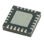
| 描述 | IC MMIC AMP VCO BUFFER 24-QFN |
| 产品分类 | RF 其它 IC 和模块 |
| 品牌 | Hittite Microwave Corporation |
| 数据手册 | 点击此处下载产品Datasheet |
| 产品图片 |  |
| 产品型号 | HMC390LP4E |
| RF类型 | 通用 |
| rohs | 无铅 / 符合限制有害物质指令(RoHS)规范要求 |
| 产品系列 | - |
| 供应商器件封装 | 24-QFN(4x4) |
| 其它名称 | 1127-1362 |
| 功能 | VCO,缓冲放大器 |
| 包装 | 剪带 |
| 封装/外壳 | 24-VFQFN 裸露焊盘 |
| 标准包装 | 100 |
| 辅助属性 | - |
| 频率 | 3.55GHz ~ 3.9GHz |
Datasheet
PDF Datasheet 数据手册内容提取
HMC390LP4 390LP4E / v02.0505 MMIC VCO w/ BUFFER AMPLIFIER, 3.55 - 3.9 GHz Typical Applications Features Low noise MMIC VCO w/Buffer Amplifi er for: Pout: +4.7 dBm • Wireless Local Loop (WLL) Phase Noise: -112 dBc/Hz @100 KHz • VSAT & Microwave Radio No External Resonator Needed • Test Equipment & Industrial Controls Single Supply: 3V @ 42 mA • Military QFN Leadless SMT Package, 16 mm2 Functional Diagram General Description 11 The HMC390LP4 & HMC390LP4E are GaAs InGaP Heterojunction Bipolar Transistor (HBT) MMIC VCOs with integrated resonators, negative resistance devices, varactor diodes, and buffer amplifi ers. T Covering 3.55 to 3.9 GHz, the VCO’s phase noise M performance is excellent over temperature, shock, S vibration and process due to the oscillator’s monolithic - structure. Power output is 4.7 dBm typical from a s single supply of 3V @ 42 mA. The voltage controlled O oscillator is packaged in a low cost leadless QFN 4 x 4 L P mm surface mount package. & S O C V Electrical Specifi cations, T = +25° C, Vcc = +3V A Parameter Min. Typ. Max. Units Frequency Range 3.55 - 3.9 GHz Power Output 1.5 4.7 dBm SSB Phase Noise @ 100 kHz Offset, Vtune= +5V @ RF Output -112 dBc/Hz Tune Voltage (Vtune) 0 10 V Supply Current (Icc) (Vcc = +3.0V) 42 mA Tune Port Leakage Current 10 μA Output Return Loss 6 dB Harmonics 2nd 5 dBc 3rd 16 dBc Pulling (into a 2.0:1 VSWR) 3.3 MHz pp Pushing @ Vtune= +5V -5 MHz/V Frequency Drift Rate 0.4 MHz/°C Information furnisheFd obyr Apnrailocge D,e dviceesl ivis ebreylie,v eadn tod bteo a cpcularacte ea nod rrdelieabrlse., Hpowleevaers, eno coFnotra pcritc He, idtteitlieve Mry, icanrdo wtoa pvleac Ce oorrdpeorsr: aAtnioanlo:g Devices, Inc., 11 - 38 rriegshptso nosf ibthiilritdy pisa artsiessu mthea2dt m0bya yAA rnelaspluolhgt faDroe mvRi citeos sua fsoedr. i,tSs p Cuescheif,i ecnaoltrmio fnossr asfnuoyb rjiendcfrt,i nt ogM ecmhAaenn gt0se 1owf8 iptha2otue4tn tnsPo otihcr eoo.t hNneore : 9OPh7noe8n T-ee2: c57h80n1o--33lo23g9y4- 4W37 a0 y0F, a(cid:127)P .xOO:r. d 9Be7or x8o n9-l12in05e6 0,a N-t 3wor3ww7wo3o.adn, aMloAg .0c2o0m6 2-9106 lTicraednesem aisr kgsr aanndte dre gbiys teimrepdli ctraatdioenm oarr kost haerrew tihsee purnodpeerr tya noyf tphaetier nret sOopre prcadtivteeen otr w riOgnehrtnss .-olf iAnneal oag tD ewvicwesw. .hAiptptilticea.tcioonm Support: Phone: 1-800-ANALOG-D
HMC390LP4 / 390LP4E v02.0505 MMIC VCO w/ BUFFER AMPLIFIER, 3.55 - 3.9 GHz Frequency vs. Tuning Voltage, T= 25°C Frequency vs. Tuning Voltage, Vcc= +3V 4.2 4.2 4.1 4.1 z) z) H 4 H 4 G G Y ( 3.9 Y ( 3.9 C C EN 3.8 EN 3.8 U U Q 3.7 Q 3.7 E E R R F 3.6 F 3.6 T T PU 3.5 Vcc=2.75V PU 3.5 +25 C T Vcc= 3.0V T +85 C U 3.4 Vcc=3.25V U 3.4 -40 C O O 3.3 3.3 3.2 3.2 0 1 2 3 4 5 6 7 8 9 10 0 1 2 3 4 5 6 7 8 9 10 TUNING VOLTAGE (VOLTS) TUNING VOLTAGE (VOLTS) 11 Output Power vs. Sensitivity vs. Tuning Voltage, Vcc= +3V Tuning Voltage, Vcc= +3V T 220 8 M 200 7 S OLT)116800 +25 C Bm) 6 - Y (MHz/V112400 +-4805 CC OWER (d 45 Os T100 P L VI T ENSITI 6800 OUTPU 23 ++-428055 CCC & P S 40 1 20 S 0 0 O 0 1 2 3 4 5 6 7 8 9 10 0 1 2 3 4 5 6 7 8 9 10 C TUNING VOLTAGE (VOLTS) TUNING VOLTAGE (VOLTS) V Phase Noise vs. Tuning Voltage Typical SSB Phase Noise @ Vtune= +5V -80 0 -10 -85 -20 SSB PHASE NOISE (dBc/Hz)----1111--110099505050 11000 K KHHzz O Offfsfseett SSB PHASE NOISE (dBc/Hz)----1111-------3210987654300000000000 -++ 428055 CCC -140 -120 -150 0 1 2 3 4 5 6 7 8 9 10 103 104 105 106 107 TUNING VOLTAGE (VOLTS) OFFSET FREQUENCY (Hz) Information furnisheFd obyr Apnrailocge D,e dviceesl ivis ebreylie,v eadn tod bteo a cpcularacte ea nod rrdelieabrlse., Hpowleevaers, eno coFnotra pcritc He, idtteitlieve Mry, icanrdo wtoa pvleac Ce oorrdpeorsr: aAtnioanlo:g Devices, Inc., responsibility is assume2d 0by AAnlaplohg aDe vRiceosa fodr i,ts Cushe, enolrm fosr afnoy rindfr,in gMemAen t0s 1of8 pa2te4n tsP ohr oothnere : 9O7ne8 T-e2c5h0no-3lo3gy4 W3 a yF, aP.xO:. 9B7ox8 9-120560, N-3or3w7o3od, MA 02062-9106 11 - 39 rights of third parties that may result from its use. Specifications subject to change without notice. No Phone: 781-329-4700 (cid:127) Order online at www.analog.com lTicraednesem aisr kgsr aanndte dre gbiys teimrepdli ctraatdioenm oarr kost haerrew tihsee purnodpeerr tya noyf tphaetier nret sOopre prcadtivteeen otr w riOgnehrtnss .-olf iAnneal oag tD ewvicwesw. .hAiptptilticea.tcioonm Support: Phone: 1-800-ANALOG-D
HMC390LP4 / 390LP4E v02.0505 MMIC VCO w/ BUFFER AMPLIFIER, 3.55 - 3.9 GHz Absolute Maximum Ratings Typical Supply Current vs. Vcc Vcc +3.5 Vdc Vcc (V) Icc (mA) Vtune 0 to +11V 2.75 35 Channel Temperature 135 °C 3.0 42 Continuous Pdiss (T = 85°C) 3.25 47 565 W (derate 6.28 mW/°C above 85°C) Note: VCO will operate over full voltage range shown above. Storage Temperature -65 to +150 °C Operating Temperature -40 to +85 °C ELECTROSTATIC SENSITIVE DEVICE OBSERVE HANDLING PRECAUTIONS 11 Outline Drawing T M S - s O L P & S O C V NOTES: 1. LEADFRAME MATERIAL: COPPER ALLOY 2. DIMENSIONS ARE IN INCHES [MILLIMETERS]. 3. LEAD SPACING TOLERANCE IS NON-CUMULATIVE 4. PAD BURR LENGTH SHALL BE 0.15mm MAXIMUM. PAD BURR HEIGHT SHALL BE 0.05mm MAXIMUM. 5. PACKAGE WARP SHALL NOT EXCEED 0.05mm. 6. ALL GROUND LEADS AND GROUND PADDLE MUST BE SOLERED TO PCB RF GROUND. 7. REFER TO HITTITE APPLICATION NOTE FOR SUGGESTED PCB LAND PATTERN Package Information Part Number Package Body Material Lead Finish MSL Rating Package Marking [3] HMC390LP4 Low Stress Injection Molded Plastic Sn/Pb Solder MSL1 [1] H390 XXXX HMC390LP4E RoHS-compliant Low Stress Injection Molded Plastic 100% matte Sn MSL1 [2] H390 XXXX [1] Max peak refl ow temperature of 235 °C [2] Max peak refl ow temperature of 260 °C [3] 4-Digit lot number XXXX Information furnisheFd obyr Apnrailocge D,e dviceesl ivis ebreylie,v eadn tod bteo a cpcularacte ea nod rrdelieabrlse., Hpowleevaers, eno coFnotra pcritc He, idtteitlieve Mry, icanrdo wtoa pvleac Ce oorrdpeorsr: aAtnioanlo:g Devices, Inc., 11 - 40 rriegshptso nosf ibthiilritdy pisa artsiessu mthea2dt m0bya yAA rnelaspluolhgt faDroe mvRi citeos sua fsoedr. i,tSs p Cuescheif,i ecnaoltrmio fnossr asfnuoyb rjiendcfrt,i nt ogM ecmhAaenn gt0se 1owf8 iptha2otue4tn tnsPo otihcr eoo.t hNneore : 9OPh7noe8n T-ee2: c57h80n1o--33lo23g9y4- 4W37 a0 y0F, a(cid:127)P .xOO:r. d 9Be7or x8o n9-l12in05e6 0,a N-t 3wor3ww7wo3o.adn, aMloAg .0c2o0m6 2-9106 lTicraednesem aisr kgsr aanndte dre gbiys teimrepdli ctraatdioenm oarr kost haerrew tihsee purnodpeerr tya noyf tphaetier nret sOopre prcadtivteeen otr w riOgnehrtnss .-olf iAnneal oag tD ewvicwesw. .hAiptptilticea.tcioonm Support: Phone: 1-800-ANALOG-D
HMC390LP4 / 390LP4E v02.0505 MMIC VCO w/ BUFFER AMPLIFIER, 3.55 - 3.9 GHz Pin Descriptions Pin Number Function Description Interface Schematic 1- 14, 17 - 19, N/C No Connection 21, 23, 24 15 GND This pin must be connected to RF & DC ground. 16 RFOUT RF output (AC coupled) 20 Vcc Supply Voltage Vcc= 3V 11 T M Control Voltage Input. Modulation port bandwidth 22 VTUNE dependent on drive source impedance. S - s GND Package bottom has an exposed metal paddle that O must be RF & DC grounded. L P & S O C V Information furnisheFd obyr Apnrailocge D,e dviceesl ivis ebreylie,v eadn tod bteo a cpcularacte ea nod rrdelieabrlse., Hpowleevaers, eno coFnotra pcritc He, idtteitlieve Mry, icanrdo wtoa pvleac Ce oorrdpeorsr: aAtnioanlo:g Devices, Inc., responsibility is assume2d 0by AAnlaplohg aDe vRiceosa fodr i,ts Cushe, enolrm fosr afnoy rindfr,in gMemAen t0s 1of8 pa2te4n tsP ohr oothnere : 9O7ne8 T-e2c5h0no-3lo3gy4 W3 a yF, aP.xO:. 9B7ox8 9-120560, N-3or3w7o3od, MA 02062-9106 11 - 41 rights of third parties that may result from its use. Specifications subject to change without notice. No Phone: 781-329-4700 (cid:127) Order online at www.analog.com lTicraednesem aisr kgsr aanndte dre gbiys teimrepdli ctraatdioenm oarr kost haerrew tihsee purnodpeerr tya noyf tphaetier nret sOopre prcadtivteeen otr w riOgnehrtnss .-olf iAnneal oag tD ewvicwesw. .hAiptptilticea.tcioonm Support: Phone: 1-800-ANALOG-D
HMC390LP4 / 390LP4E v02.0505 MMIC VCO w/ BUFFER AMPLIFIER, 3.55 - 3.9 GHz Evaluation PCB 11 T M S - s O L P & S O C V List of Materials for Evaluation PCB 105706 [1] The circuit board used in the fi nal application should Item Description use RF circuit design techniques. Signal lines J1 - J2 PCB Mount SMA RF Connector should have 50 ohm impedance while the package J3 - J4 DC Pin ground leads and exposed paddle should be con- C1 4.7 μF Tantalum Capacitor nected directly to the ground plane similar to that C2 10,000 pF Capacitor, 0603 Pkg. shown. A sufficient number of via holes should be U1 HMC390LP4 / HMC390LP4E VCO used to connect the top and bottom ground planes. PCB* 105667 Eval Board The evaluation circuit board shown is available from [1] Reference this number when ordering complete evaluation PCB Hittite upon request. [2] Circuit Board Material: Rogers 4350 Information furnisheFd obyr Apnrailocge D,e dviceesl ivis ebreylie,v eadn tod bteo a cpcularacte ea nod rrdelieabrlse., Hpowleevaers, eno coFnotra pcritc He, idtteitlieve Mry, icanrdo wtoa pvleac Ce oorrdpeorsr: aAtnioanlo:g Devices, Inc., 11 - 42 rriegshptso nosf ibthiilritdy pisa artsiessu mthea2dt m0bya yAA rnelaspluolhgt faDroe mvRi citeos sua fsoedr. i,tSs p Cuescheif,i ecnaoltrmio fnossr asfnuoyb rjiendcfrt,i nt ogM ecmhAaenn gt0se 1owf8 iptha2otue4tn tnsPo otihcr eoo.t hNneore : 9OPh7noe8n T-ee2: c57h80n1o--33lo23g9y4- 4W37 a0 y0F, a(cid:127)P .xOO:r. d 9Be7or x8o n9-l12in05e6 0,a N-t 3wor3ww7wo3o.adn, aMloAg .0c2o0m6 2-9106 lTicraednesem aisr kgsr aanndte dre gbiys teimrepdli ctraatdioenm oarr kost haerrew tihsee purnodpeerr tya noyf tphaetier nret sOopre prcadtivteeen otr w riOgnehrtnss .-olf iAnneal oag tD ewvicwesw. .hAiptptilticea.tcioonm Support: Phone: 1-800-ANALOG-D
HMC390LP4 / 390LP4E v02.0505 MMIC VCO w/ BUFFER AMPLIFIER, 3.55 - 3.9 GHz Notes: 11 T M S - s O L P & S O C V Information furnisheFd obyr Apnrailocge D,e dviceesl ivis ebreylie,v eadn tod bteo a cpcularacte ea nod rrdelieabrlse., Hpowleevaers, eno coFnotra pcritc He, idtteitlieve Mry, icanrdo wtoa pvleac Ce oorrdpeorsr: aAtnioanlo:g Devices, Inc., responsibility is assume2d 0by AAnlaplohg aDe vRiceosa fodr i,ts Cushe, enolrm fosr afnoy rindfr,in gMemAen t0s 1of8 pa2te4n tsP ohr oothnere : 9O7ne8 T-e2c5h0no-3lo3gy4 W3 a yF, aP.xO:. 9B7ox8 9-120560, N-3or3w7o3od, MA 02062-9106 11 - 43 rights of third parties that may result from its use. Specifications subject to change without notice. No Phone: 781-329-4700 (cid:127) Order online at www.analog.com lTicraednesem aisr kgsr aanndte dre gbiys teimrepdli ctraatdioenm oarr kost haerrew tihsee purnodpeerr tya noyf tphaetier nret sOopre prcadtivteeen otr w riOgnehrtnss .-olf iAnneal oag tD ewvicwesw. .hAiptptilticea.tcioonm Support: Phone: 1-800-ANALOG-D
Mouser Electronics Authorized Distributor Click to View Pricing, Inventory, Delivery & Lifecycle Information: A nalog Devices Inc.: HMC390LP4E HMC390LP4ETR HMC390LP4 HMC390LP4TR 105706-HMC390LP4