首页 > HMC363S8GE > 详情
 Datasheet下载
- 型号: HMC363S8GE
- 制造商: Hittite
- 库位|库存: xxxx|xxxx
- 要求:
| 数量阶梯 | 香港交货 | 国内含税 |
| +xxxx | $xxxx | ¥xxxx |
查看当月历史价格
查看今年历史价格
产品参数
| 参数 | 数值 |
| 产品目录 | 射频/IF 和 RFID |
| 描述 | IC FREQ DIVIDER DC-12GHZ 8SOIC |
| 产品分类 | RF 其它 IC 和模块 |
| 品牌 | Hittite Microwave Corporation |
| 数据手册 | 点击此处下载产品Datasheet |
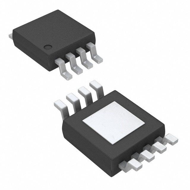
| 产品图片 |  |
| 产品型号 | HMC363S8GE |
| RF类型 | 通用 |
| rohs | 无铅 / 符合限制有害物质指令(RoHS)规范要求 |
| 产品系列 | - |
| 供应商器件封装 | 8-SMT |
| 其它名称 | 1127-1028-2 HMC363S8GETR |
| 功能 | 预定标器 |
| 包装 | 带卷 (TR) |
| 封装/外壳 | 8-SOIC(0.154",3.90mm 宽)裸焊盘 |
| 标准包装 | 500 |
| 辅助属性 | 8 分型 |
| 频率 | 0Hz ~ 12GHz |
Datasheet
PDF Datasheet 数据手册内容提取
HMC363S8G / 363S3GE v05.0412 SMT GaAs HBT MMIC DIVIDE-BY-8, DC - 12 GHz Typical Applications Features Prescaler for Dc to X Band PLL Applications: ultra Low ssB Phase noise: -153 dBc/Hz t • Satellite Communication Systems Wide Bandwidth M • Fiber Optic output Power: -6 dBm s • Point-to-Point and Point-to-Multi-Point Radios single Dc supply: +5v - s • VSAT s8G sMt Package r o t c Functional Diagram General Description e the HMc363s8G & HMc363s8Ge are low noise t e Divide-by-8 static Dividers with inGaP GaAs HBt D technology in 8 lead surface mount plastic packages. this device operates from Dc (with a square wave & input) to 12 GHz input frequency with a single +5v s Dc supply. the low additive ssB phase noise of r -153 dBc/Hz at 100 kHz offset helps the user maintain e good system noise performance. D i v i D y c n e u q e r Electrical Specifications, T = +25° C, 50 Ohm System, Vcc= 5V A F Parameter conditions Min. typ. Max. units Maximum input Frequency 12 13 GHz Minimum input Frequency sine Wave input. [1] 0.2 0.5 GHz input Power range Fin = 1 to 7 GHz -15 >-20 +10 dBm Fin = 7 to 11 GHz -10 >-15 +2 dBm Fin = 11 to 12 GHz -5 >-8 0 dBm output Power Fin = 12 GHz -9 -6 dBm reverse Leakage Both rF outputs terminated 65 dB ssB Phase noise (100 kHz offset) Pin = 0 dBm, Fin = 6 GHz -153 dBc/Hz output transition time Pin = 0 dBm, Fout = 882 MHz 100 ps supply current (icc) 70 mA 1. Divider will operate down to DC for square-wave input signal. InfoFrmoart iopn rfiucrneis,h edde blyi vAenraylo ga Dnedvic teos ips lbaelcieeve do rtod beer sac:c Huraittet iatned Mreliiacbrleo. wHoawveeve rC, noo rpoForar tpioricne,, 2d eElilviezrayb, aentdh tDo rpivlaec,e C ohrdeelrms: sAfonardlo,g MDeAv i0ce1s8, 2In4c., responsibility is assumed by Analog Devices for its use, nor for any infringements of patents or other One Technology Way, P.O. Box 9106, Norwood, MA 02062-9106 1 rliicgehntss eo fi sth girrda nptaerdti ebsy t himatp mlicaaPyt iorhenso uonlrt ofertoh:m e9r wit7sis 8ues -eu2.n dS5ep0re ca-inf3iyc 3aptia4otne3sn ts ou rb jpeFacttae tnoxt c:r hig9ahn7tgs 8eo wf- 2Aithn5oau0lot g-n 3oDti3ecve7i.c 3eNso . POhrodnee:r 7 O81n-3-l2i9n-e4 7a0t0 w(cid:127) wOrwde.hr oitntliitnee. cato wmww.analog.com Trademarks and registered trademarks arAe tphep plriocpearttyi oof nth eSir urepsppecotivret :o wPnehrso.ne: 978-250-3A3p4p3li c aotrio na Spuppsp@orht: iPtthitoen.ec: o1-m800-ANALOG-D
HMC363S8G / 363S3GE v05.0412 SMT GaAs HBT MMIC DIVIDE-BY-8, DC - 12 GHz Input Sensitivity Window, T= 25 °C Input Sensitivity Window vs. Temperature 20 20 t 10 10 M m) m) dB dB s R ( 0 Recommended R ( 0 E E Min Pin +25 C W Operating Window W Max Pin +25 C - O O Min Pin +85 C T P-10 T P-10 MMaixn PPinin +-8450 CC s PU PU Max Pin -40 C r N N I-20 I-20 o t -30 -30 c 0 3 6 9 12 15 0 3 6 9 12 15 e INPUT FREQUENCY (GHz) INPUT FREQUENCY (GHz) t e D SSB Phase Noise Output Power vs. Temperature Performance, Pin= 0 dBm, T= 25 °C & 0 0 s -20 r ER (dBm) --42 ++-428055 CCC SE (dBc/Hz) --6400 iDe OW NOI -80 v UT P -6 ASE -100 Di OUTP -8 SB PH-120 y S-140 c n -10 -160 0 3 6 9 12 15 102 103 104 105 106 107 e INPUT FREQUENCY (GHz) OFFSET FREQUENCY (Hz) u q e Output Harmonic r Content, Pin= 0 dBm, T= 25 °C Reverse Leakage, Pin= 0 dBm, T= 25 °C F 0 0 -10 Both Output Ports Terminated m) m)-20 One Output Port Terminated EL (dB-20 EL (dB EV-30 EV-40 TPUT L-40 WER L OU PO-60 -50 2Pnfde eHdathrmruonic 3rd Harmonic -60 -80 0 3 6 9 12 15 0 3 6 9 12 15 INPUT FREQUENCY (GHz) INPUT FREQUENCY (GHz) InfoFrmoart iopn rfiucrneis,h edde blyi vAenraylo ga Dnedvic teos ips lbaelcieeve do rtod beer sac:c Huraittet iatned Mreliiacbrleo. wHoawveeve rC, noo rpoForar tpioricne,, 2d eElilviezrayb, aentdh tDo rpivlaec,e C ohrdeelrms: sAfonardlo,g MDeAv i0ce1s8, 2In4c., responsibility is assumed by Analog Devices for its use, nor for any infringements of patents or other One Technology Way, P.O. Box 9106, Norwood, MA 02062-9106 rights of third parties that maPy rhesounlt fero:m 9 it7s 8us-e2. S5p0ec-if3ic3ati4on3s s u b jeFcta tox c: h9an7g8e w-2ith5ou0t -n3oti3ce7. 3No POhrodnee:r 7 O81n-3-l2i9n-e4 7a0t0 w(cid:127) wOrwde.hr oitntliitnee. cato wmww.analog.com 2 license is granted by implication or otherwise under any patent or patent rights of Analog Devices. Trademarks and registered trademarks arAe tphep plriocpearttyi oof nth eSir urepsppecotivret :o wPnehrso.ne: 978-250-3A3p4p3li c aotrio na Spuppsp@orht: iPtthitoen.ec: o1-m800-ANALOG-D
HMC363S8G / 363S3GE v05.0412 SMT GaAs HBT MMIC DIVIDE-BY-8, DC - 12 GHz Output Voltage Waveform, Pin= 0 dBm, Fout= 882 MHz, T= 25 °C 300 t 200 M s mV)100 E ( s - LITUD 0 P r M-100 A o -200 t c -300 e 22.7 23.1 23.5 23.9 24.3 24.7 TIME (nS) t e D Absolute Maximum Ratings Typical Supply Current vs. Vcc & s rF input (vcc = +5v) +13 dBm vcc (v) icc (mA) r vcc +5.5v 4.75 64 e channel temperature 135 °c 5.0 70 D continuous Pdiss (t=85°c) 5.25 75 680 mW i (derate 13.7 mW/°c above 85°c) v note: Divider will operate over full voltage range shown above thermal resistance i 73.2 c/W D (channel to ground paddle) y storage temperature -65 to +150 °c eLectrostAtic sensitive Device c operating temperature -40 to +85 °c oBserve HAnDLinG PrecAutions n e u q e r F InfoFrmoart iopn rfiucrneis,h edde blyi vAenraylo ga Dnedvic teos ips lbaelcieeve do rtod beer sac:c Huraittet iatned Mreliiacbrleo. wHoawveeve rC, noo rpoForar tpioricne,, 2d eElilviezrayb, aentdh tDo rpivlaec,e C ohrdeelrms: sAfonardlo,g MDeAv i0ce1s8, 2In4c., responsibility is assumed by Analog Devices for its use, nor for any infringements of patents or other One Technology Way, P.O. Box 9106, Norwood, MA 02062-9106 3 rliicgehntss eo fi sth girrda nptaerdti ebsy t himatp mlicaaPyt iorhenso uonlrt ofertoh:m e9r wit7sis 8ues -eu2.n dS5ep0re ca-inf3iyc 3aptia4otne3sn ts ou rb jpeFacttae tnoxt c:r hig9ahn7tgs 8eo wf- 2Aithn5oau0lot g-n 3oDti3ecve7i.c 3eNso . POhrodnee:r 7 O81n-3-l2i9n-e4 7a0t0 w(cid:127) wOrwde.hr oitntliitnee. cato wmww.analog.com Trademarks and registered trademarks arAe tphep plriocpearttyi oof nth eSir urepsppecotivret :o wPnehrso.ne: 978-250-3A3p4p3li c aotrio na Spuppsp@orht: iPtthitoen.ec: o1-m800-ANALOG-D
HMC363S8G / 363S3GE v05.0412 SMT GaAs HBT MMIC DIVIDE-BY-8, DC - 12 GHz Outline Drawing t M s - s r o t c e t e D notes: 1. LeADFrAMe MAteriAL: coPPer ALLoy & 2. DiMensions Are in incHes [MiLLiMeters] 3. DiMension Does not incLuDe MoLDFLAsH oF 0.15mm Per siDe. s 4. DiMension Does not incLuDe MoLDFLAsH oF 0.25mm Per siDe. r 5. ALL GrounD LeADs AnD GrounD PADDLe Must Be soLDereD to PcB rF GrounD. e D i v Package Information i D Part number Package Body Material Lead Finish MsL rating Package Marking [3] y HMc363s8G Low stress injection Molded Plastic sn/Pb solder MsL1 [1] HMc363 c XXXX n HMc363s8Ge roHs-compliant Low stress injection Molded Plastic 100% matte sn MsL1 [2] HMc363 XXXX e [1] Max peak reflow temperature of 235 °c u [2] Max peak reflow temperature of 260 °c q [3] 4-Digit lot number XXXX e r F InfoFrmoart iopn rfiucrneis,h edde blyi vAenraylo ga Dnedvic teos ips lbaelcieeve do rtod beer sac:c Huraittet iatned Mreliiacbrleo. wHoawveeve rC, noo rpoForar tpioricne,, 2d eElilviezrayb, aentdh tDo rpivlaec,e C ohrdeelrms: sAfonardlo,g MDeAv i0ce1s8, 2In4c., responsibility is assumed by Analog Devices for its use, nor for any infringements of patents or other One Technology Way, P.O. Box 9106, Norwood, MA 02062-9106 rights of third parties that maPy rhesounlt fero:m 9 it7s 8us-e2. S5p0ec-if3ic3ati4on3s s u b jeFcta tox c: h9an7g8e w-2ith5ou0t -n3oti3ce7. 3No POhrodnee:r 7 O81n-3-l2i9n-e4 7a0t0 w(cid:127) wOrwde.hr oitntliitnee. cato wmww.analog.com 4 license is granted by implication or otherwise under any patent or patent rights of Analog Devices. Trademarks and registered trademarks arAe tphep plriocpearttyi oof nth eSir urepsppecotivret :o wPnehrso.ne: 978-250-3A3p4p3li c aotrio na Spuppsp@orht: iPtthitoen.ec: o1-m800-ANALOG-D
HMC363S8G / 363S3GE v05.0412 SMT GaAs HBT MMIC DIVIDE-BY-8, DC - 12 GHz Pin Description Pin number Function Description interface schematic t M s 1 nout Divided output 180° out of phase with pin 3. - s r 2, 6 n/c no connection. these pins must not be grounded. o t c 3 out Divided output. e t e D & 4 vcc supply voltage 5v ± 0.25v. s r e D 5 in rF input must be Dc blocked. i v i D y rF input 180° out of phase with pin 5 for differential operation. c 7 nin A/c ground for single ended operation n e u Backside of package has exposed metal ground slug which q 8, paddle GnD must be connected to ground. e r Application Circuit F InfoFrmoart iopn rfiucrneis,h edde blyi vAenraylo ga Dnedvic teos ips lbaelcieeve do rtod beer sac:c Huraittet iatned Mreliiacbrleo. wHoawveeve rC, noo rpoForar tpioricne,, 2d eElilviezrayb, aentdh tDo rpivlaec,e C ohrdeelrms: sAfonardlo,g MDeAv i0ce1s8, 2In4c., responsibility is assumed by Analog Devices for its use, nor for any infringements of patents or other One Technology Way, P.O. Box 9106, Norwood, MA 02062-9106 5 rliicgehntss eo fi sth girrda nptaerdti ebsy t himatp mlicaaPyt iorhenso uonlrt ofertoh:m e9r wit7sis 8ues -eu2.n dS5ep0re ca-inf3iyc 3aptia4otne3sn ts ou rb jpeFacttae tnoxt c:r hig9ahn7tgs 8eo wf- 2Aithn5oau0lot g-n 3oDti3ecve7i.c 3eNso . POhrodnee:r 7 O81n-3-l2i9n-e4 7a0t0 w(cid:127) wOrwde.hr oitntliitnee. cato wmww.analog.com Trademarks and registered trademarks arAe tphep plriocpearttyi oof nth eSir urepsppecotivret :o wPnehrso.ne: 978-250-3A3p4p3li c aotrio na Spuppsp@orht: iPtthitoen.ec: o1-m800-ANALOG-D
HMC363S8G / 363S3GE v05.0412 SMT GaAs HBT MMIC DIVIDE-BY-8, DC - 12 GHz Evaluation PCB t M s - s r o t c e t e D & s r e D i v i D y c n e u q e List of Materials for Evaluation PCB 104631 [1] r F the circuit board used in the application should use item Description rF circuit design techniques. signal lines should J1 - J3 PcB Mount sMA rF connector have 50 ohm impedance while the package ground c1 - c4 100 pF capacitor, 0402 Pkg. leads and backside ground slug should be con- c5 1000 pF capacitor, 0603 Pkg. nected directly to the ground plane similar to that c6 10 µF tantalum capacitor shown. A sufficient number of via holes should be u1 HMc363s8G / HMc363s8Ge Divide-by-8 used to connect the top and bottom ground planes. PcB [2] 104627 eval Board the evaluation circuit board shown is available [1] reference this number when ordering complete evaluation PcB from Hittite upon request. this evaluation board is [2] circuit Board Material: rogers 4350 designed for single ended input testing. J2 and J3 provide differential output signals. InfoFrmoart iopn rfiucrneis,h edde blyi vAenraylo ga Dnedvic teos ips lbaelcieeve do rtod beer sac:c Huraittet iatned Mreliiacbrleo. wHoawveeve rC, noo rpoForar tpioricne,, 2d eElilviezrayb, aentdh tDo rpivlaec,e C ohrdeelrms: sAfonardlo,g MDeAv i0ce1s8, 2In4c., responsibility is assumed by Analog Devices for its use, nor for any infringements of patents or other One Technology Way, P.O. Box 9106, Norwood, MA 02062-9106 rights of third parties that maPy rhesounlt fero:m 9 it7s 8us-e2. S5p0ec-if3ic3ati4on3s s u b jeFcta tox c: h9an7g8e w-2ith5ou0t -n3oti3ce7. 3No POhrodnee:r 7 O81n-3-l2i9n-e4 7a0t0 w(cid:127) wOrwde.hr oitntliitnee. cato wmww.analog.com 6 license is granted by implication or otherwise under any patent or patent rights of Analog Devices. Trademarks and registered trademarks arAe tphep plriocpearttyi oof nth eSir urepsppecotivret :o wPnehrso.ne: 978-250-3A3p4p3li c aotrio na Spuppsp@orht: iPtthitoen.ec: o1-m800-ANALOG-D