首页 > HMC344LP3E > 详情
 Datasheet下载
- 型号: HMC344LP3E
- 制造商: Hittite
- 库位|库存: xxxx|xxxx
- 要求:
| 数量阶梯 | 香港交货 | 国内含税 |
| +xxxx | $xxxx | ¥xxxx |
查看当月历史价格
查看今年历史价格
产品参数
| 参数 | 数值 |
| 产品目录 | 射频/IF 和 RFID |
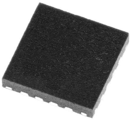
| 描述 | IC SWITCH SP4T DC-8GHZ 16-QFN |
| 产品分类 | RF 开关 |
| IIP3 | 40dBm (标准) |
| 品牌 | Hittite Microwave Corporation |
| 数据手册 | 点击此处下载产品Datasheet |
| 产品图片 |  |
| P1dB | 21dBm (标准) IP1dB |
| 产品型号 | HMC344LP3E |
| RF类型 | WLAN |
| rohs | 无铅 / 符合限制有害物质指令(RoHS)规范要求 |
| 产品系列 | - |
| 供应商器件封装 | 16-QFN(3x3) |
| 其它名称 | 1127-1339 1127-1339-1 1127-1339-ND |
| 包装 | Digi-Reel® |
| 封装/外壳 | 16-VFQFN 裸露焊盘 |
| 工作温度 | -40°C ~ 85°C |
| 拓扑 | 吸收性 |
| 插损@频率 | 1.8dB @ 6GHz |
| 标准包装 | 1 |
| 特性 | - |
| 电压-电源 | - |
| 电路 | SP4T |
| 阻抗 | 50 欧姆 |
| 隔离@频率 | 40dB @ 6GHz (标准) |
| 频率 -上 | 8GHz |
| 频率 -下 | 0Hz |
Datasheet
PDF Datasheet 数据手册内容提取
HMC344LP3 344LP3E / v06.1210 GaAs MMIC SP4T NON-REFLECTIVE SWITCH, DC - 8 GHz Typical Applications Features this switch is suitable for usage in Dc - 8.0 Ghz 50- Broadband Performance: Dc - 8 Ghz ohm or 75-ohm systems: high isolation: 40 dB@ 6 Ghz • Broadband low insertion loss: 1.8 dB@ 6 Ghz • Fiber Optics integrated 2:4 ttl Decoder • Switched Filter Banks 16 lead 3x3mm QFN Package: 9 mm² • Wireless below 8 GHz Functional Diagram General Description the hmc344lP3 & hmc344lP3e are broadband non-reflective GaAs meSFet SP4t switches in low cost leadless surface mount packages. covering Dc to 8 Ghz, this switch offers high isolation and low insertion loss and extends the frequency coverage of hittite’s SP4t switch product line. this switch also 15 includes an on board binary decoder circuit which reduces the required logic control lines to two. the switch operates using a negative control voltage of 0/-5V, and requires a fixed bias of -5V. t m S - w o r Electrical Specifications, T = +25° C, With 0/-5V Control, 50 Ohm System h A t Parameter Frequency min. typ. max. units - i Dc - 2.0 Ghz 1.6 2.0 dB t insertion loss Dc - 6.0 Ghz 1.8 2.2 dB l Dc - 8.0 Ghz 2.1 2.5 dB u Dc - 2.0 Ghz 43 48 dB m Dc - 4.0 Ghz 36 41 dB isolation Dc - 6.0 Ghz 34 40 dB - Dc - 8.0 Ghz 31 36 dB S Dc - 2.0 Ghz 12 15 dB e Dc - 4.0 Ghz 9 12 dB return loss “on State” h Dc - 6.0 Ghz 8 11 dB Dc - 8.0 Ghz 5 8 dB c return loss “off State” Dc - 8.0 Ghz 7 10 dB t i input Power for 1 dB compression 0.5 - 8.0 Ghz 17 21 dBm w input third order intercept 0.5 - 8.0 Ghz 37 40 dBm S (two-tone input Power = +7 dBm each tone) Switching characteristics 35 ns triSe, tFAll (10/90% rF) Dc - 8.0 Ghz 150 ns toN, toFF (50% ctl to 10/90% rF) InforFmaotiro np fruircniseh,e dd beyl iAvnealroyg Daenvidce st ois pbelaliecveed otor dbee arcsc:u rHateit taintde reMliaibcler. oHwowaevveer, Cnoo rpFoorr aptriiocen,, d2e0liv Aerlyp, haand R too apdla,c Ce horedlemrss: fAonrdal,o gM DAe v0ic1e8s2, 4Inc., responsibility is assumed by Analog Devices for its use, nor for any infringements of patents or other One Technology Way, P.O. Box 9106, Norwood, MA 02062-9106 15 - 1 rliicgehntss eo fi sth girrda nptaerdti ebsy t himatp mlicaaPyt iorhenso uonlrt ofertoh:m e9r wit7sis 8ues -eu2.n dS5ep0re ca-inf3iyc 3aptia4otne3sn ts ou rb jpeFacttae tnoxt c:r hig9ahn7tgs 8eo wf- 2Aithn5oau0lot g-n 3oDti3ecve7i.c 3eNso . POhrodnee:r 7 O81n-3-l2i9n-e4 7a0t0 w(cid:127) wOrwde.hr oitntliitnee. cato wmww.analog.com Trademarks and registered trademarks arAe tphep plriocpearttyi oof nth eSir urepsppecotivret :o wPnehrso.ne: 978-250-3A3p4p3li c aotrio na Spuppsp@orht: iPtthitoen.ec: o1-m800-ANALOG-D
HMC344LP3 / 344LP3E v06.1210 GaAs MMIC SP4T NON-REFLECTIVE SWITCH, DC - 8 GHz Insertion Loss vs. Temperature Isolation 0 0 -10 RF1 -1 RF2 dB) -20 RRFF34 OSS ( -2 N (dB)-30 RTION L -3 OLATIO-40 SE IS-50 N +25 C I -4 +85 C -40 C -60 -5 -70 0 1 2 3 4 5 6 7 8 9 0 1 2 3 4 5 6 7 8 9 10 FREQUENCY (GHz) FREQUENCY (GHz) Return Loss 0.1 and 1 dB Input Compression Point 0 25 -5 RRFFC1,2,3,4 On T (dBm) 22 15 dB) RF1,2,3,4 Off OIN S (-10 N P 19 S O RN LO-15 RESSI 16 mt U P RET OM S -20 T C 13 10..01ddBB CCoommpprreessssiioonn PPooiinntt PU - N I w -25 10 0 1 2 3 4 5 6 7 8 9 2 3 4 5 6 7 8 9 o FREQUENCY (GHz) FREQUENCY (GHz) r h t Input Third Order Intercept Point Bias Voltage & Current - i t m) 45 Vee range = -5.0 Vdc ± 10% l PT (dB 43 (VVedec) iee(m (tAy)p.) iee( m(mAa)x.) mu E RC -5.0 3.0 6.0 E - NT 41 R I S RDE 39 Control Voltages e O h HIRD 37 RRFF12 State Bias condition c T RF3 low -3V to 0 Vdc @ 60 µA typical T RF4 t U P high -5 to -4.2 Vdc @ 5 µA typical i N 35 w I 1 2 3 4 5 6 7 8 9 FREQUENCY (GHz) S * Isolation is recorded above insertion loss & measured at output of switch. InforFmaotiro np fruircniseh,e dd beyl iAvnealroyg Daenvidce st ois pbelaliecveed otor dbee arcsc:u rHateit taintde reMliaibcler. oHwowaevveer, Cnoo rpFoorr aptriiocen,, d2e0liv Aerlyp, haand R too apdla,c Ce horedlemrss: fAonrdal,o gM DAe v0ic1e8s2, 4Inc., responsibility is assumed by Analog Devices for its use, nor for any infringements of patents or other One Technology Way, P.O. Box 9106, Norwood, MA 02062-9106 rights of third parties that maPy rhesounlt fero:m 9 it7s 8us-e2. S5p0ec-if3ic3ati4on3s s u b jeFcta tox c: h9an7g8e w-2ith5ou0t -n3oti3ce7. 3No POhrodnee:r 7 O81n-3-l2i9n-e4 7a0t0 w(cid:127) wOrwde.hr oitntliitnee. cato wmww.analog.com 15 - 2 license is granted by implication or otherwise under any patent or patent rights of Analog Devices. Trademarks and registered trademarks arAe tphep plriocpearttyi oof nth eSir urepsppecotivret :o wPnehrso.ne: 978-250-3A3p4p3li c aotrio na Spuppsp@orht: iPtthitoen.ec: o1-m800-ANALOG-D
HMC344LP3 / 344LP3E v06.1210 GaAs MMIC SP4T NON-REFLECTIVE SWITCH, DC - 8 GHz Absolute Maximum Ratings Truth Table Bias Voltage range (Vee) -7.0 Vdc control input Signal Path State control Voltage range (A & B) Vee -0.5V to +1.0 Vdc A B rFcom to: channel temperature 150 °c high high rF1 thermal resistance low high rF2 143 °c/w (insertion loss Path) high low rF3 thermal resistance 1,030 °c/w low low rF4 (terminated Path) Storage temperature -65 to +150 °c operating temperature -40 to +85 °c electroStAtic SeNSitiVe DeVice oBSerVe hANDliNG PrecAutioNS maximum input Power +24 dBm eSD Sensitivity (hBm) class 1A Outline Drawing 15 t m S - w o r h NoteS: t 1. leADFrAme mAteriAl: coPPer AlloY - 2. DimeNSioNS Are iN iNcheS [millimeterS]. i t 3. leAD SPAciNG tolerANce iS NoN-cumulAtiVe l 4. PAD Burr leNGth ShAll Be 0.15mm mAXimum. u PAD Burr heiGht ShAll Be 0.05mm mAXimum. 5. PAcKAGe wArP ShAll Not eXceeD 0.05mm. m 6. All GrouND leADS AND GrouND PADDle muSt Be SolDereD to PcB rF GrouND. - 7. reFer to hittite APPlicAtioN Note For SuGGeSteD PcB lAND S PAtterN. e h Package Information c Part Number Package Body material lead Finish mSl rating Package marking [3] t wi hmc344lP3 low Stress injection molded Plastic Sn/Pb Solder mSl1 [1] X3X4X4X S hmc344lP3e rohS-compliant low Stress injection molded Plastic 100% matte Sn mSl1 [2] 344 XXXX [1] max peak reflow temperature of 235 °c [2] max peak reflow temperature of 260 °c [3] 4-Digit lot number XXXX InforFmaotiro np fruircniseh,e dd beyl iAvnealroyg Daenvidce st ois pbelaliecveed otor dbee arcsc:u rHateit taintde reMliaibcler. oHwowaevveer, Cnoo rpFoorr aptriiocen,, d2e0liv Aerlyp, haand R too apdla,c Ce horedlemrss: fAonrdal,o gM DAe v0ic1e8s2, 4Inc., responsibility is assumed by Analog Devices for its use, nor for any infringements of patents or other One Technology Way, P.O. Box 9106, Norwood, MA 02062-9106 15 - 3 rliicgehntss eo fi sth girrda nptaerdti ebsy t himatp mlicaaPyt iorhenso uonlrt ofertoh:m e9r wit7sis 8ues -eu2.n dS5ep0re ca-inf3iyc 3aptia4otne3sn ts ou rb jpeFacttae tnoxt c:r hig9ahn7tgs 8eo wf- 2Aithn5oau0lot g-n 3oDti3ecve7i.c 3eNso . POhrodnee:r 7 O81n-3-l2i9n-e4 7a0t0 w(cid:127) wOrwde.hr oitntliitnee. cato wmww.analog.com Trademarks and registered trademarks arAe tphep plriocpearttyi oof nth eSir urepsppecotivret :o wPnehrso.ne: 978-250-3A3p4p3li c aotrio na Spuppsp@orht: iPtthitoen.ec: o1-m800-ANALOG-D
HMC344LP3 / 344LP3E v06.1210 GaAs MMIC SP4T NON-REFLECTIVE SWITCH, DC - 8 GHz Pin Descriptions Pin Number Function Description interface Schematic 1, 4, rF4, rF3, rF2, this pin is Dc coupled and matched to 50 ohm. Blocking 9, 12, 15 rF1, rFc capacitors are required if rF line potential is not equal to 0V. 2, 3, this pin should be connected to PcB rF N/c 10, 11, 13 ground to maximize isolation. Package bottom has exposed metal paddle that 5, 14, 16 GND must also be connected to PcB rF ground. 6 Vee Supply Voltage -5V ± 10% 7 ctlB See truth table and control voltage table. 15 8 ctlA See truth table and control voltage table. t m S - w o r h t - i t l u m - S e h c t i w S InforFmaotiro np fruircniseh,e dd beyl iAvnealroyg Daenvidce st ois pbelaliecveed otor dbee arcsc:u rHateit taintde reMliaibcler. oHwowaevveer, Cnoo rpFoorr aptriiocen,, d2e0liv Aerlyp, haand R too apdla,c Ce horedlemrss: fAonrdal,o gM DAe v0ic1e8s2, 4Inc., responsibility is assumed by Analog Devices for its use, nor for any infringements of patents or other One Technology Way, P.O. Box 9106, Norwood, MA 02062-9106 rights of third parties that maPy rhesounlt fero:m 9 it7s 8us-e2. S5p0ec-if3ic3ati4on3s s u b jeFcta tox c: h9an7g8e w-2ith5ou0t -n3oti3ce7. 3No POhrodnee:r 7 O81n-3-l2i9n-e4 7a0t0 w(cid:127) wOrwde.hr oitntliitnee. cato wmww.analog.com 15 - 4 license is granted by implication or otherwise under any patent or patent rights of Analog Devices. Trademarks and registered trademarks arAe tphep plriocpearttyi oof nth eSir urepsppecotivret :o wPnehrso.ne: 978-250-3A3p4p3li c aotrio na Spuppsp@orht: iPtthitoen.ec: o1-m800-ANALOG-D
HMC344LP3 / 344LP3E v06.1210 GaAs MMIC SP4T NON-REFLECTIVE SWITCH, DC - 8 GHz TTL Interface Circuit 15 t m S - w o r h t - i t l u m - S e h c t i w S InforFmaotiro np fruircniseh,e dd beyl iAvnealroyg Daenvidce st ois pbelaliecveed otor dbee arcsc:u rHateit taintde reMliaibcler. oHwowaevveer, Cnoo rpFoorr aptriiocen,, d2e0liv Aerlyp, haand R too apdla,c Ce horedlemrss: fAonrdal,o gM DAe v0ic1e8s2, 4Inc., responsibility is assumed by Analog Devices for its use, nor for any infringements of patents or other One Technology Way, P.O. Box 9106, Norwood, MA 02062-9106 15 - 5 rliicgehntss eo fi sth girrda nptaerdti ebsy t himatp mlicaaPyt iorhenso uonlrt ofertoh:m e9r wit7sis 8ues -eu2.n dS5ep0re ca-inf3iyc 3aptia4otne3sn ts ou rb jpeFacttae tnoxt c:r hig9ahn7tgs 8eo wf- 2Aithn5oau0lot g-n 3oDti3ecve7i.c 3eNso . POhrodnee:r 7 O81n-3-l2i9n-e4 7a0t0 w(cid:127) wOrwde.hr oitntliitnee. cato wmww.analog.com Trademarks and registered trademarks arAe tphep plriocpearttyi oof nth eSir urepsppecotivret :o wPnehrso.ne: 978-250-3A3p4p3li c aotrio na Spuppsp@orht: iPtthitoen.ec: o1-m800-ANALOG-D
HMC344LP3 / 344LP3E v06.1210 GaAs MMIC SP4T NON-REFLECTIVE SWITCH, DC - 8 GHz Evaluation PCB 15 t m S - w o r h t List of Materials for Evaluation PCB 105311 [1] - i t the circuit board used in the final application item Description l J1 - J7 PcB mount SmA rF connector should be generated with proper rF circuit design u techniques. Signal lines at the rF port should have m J8 - J11 Dc Pin 50 ohm impedance and the package ground leads c1 - c7 0 ohm res, 0402 Pkg. [3] - and backside ground slug should be connected c8 10k pF capacitor, 0603 Pkg. S directly to the ground plane similar to that shown hmc344lP3 / hmc344lP3e e u1 SP4t Switch above. the evaluation circuit board shown above is h PcB [2] 104708 evaluation PcB 1.29”x1.55” available from hittite microwave corporation upon c [1] reference this number when ordering complete evaluation PcB request. t [2] circuit Board material: rogers 4350 i w [3] Select and replace with a suitable capacitor value for applicable operating frequency range. S InforFmaotiro np fruircniseh,e dd beyl iAvnealroyg Daenvidce st ois pbelaliecveed otor dbee arcsc:u rHateit taintde reMliaibcler. oHwowaevveer, Cnoo rpFoorr aptriiocen,, d2e0liv Aerlyp, haand R too apdla,c Ce horedlemrss: fAonrdal,o gM DAe v0ic1e8s2, 4Inc., responsibility is assumed by Analog Devices for its use, nor for any infringements of patents or other One Technology Way, P.O. Box 9106, Norwood, MA 02062-9106 rights of third parties that maPy rhesounlt fero:m 9 it7s 8us-e2. S5p0ec-if3ic3ati4on3s s u b jeFcta tox c: h9an7g8e w-2ith5ou0t -n3oti3ce7. 3No POhrodnee:r 7 O81n-3-l2i9n-e4 7a0t0 w(cid:127) wOrwde.hr oitntliitnee. cato wmww.analog.com 15 - 6 license is granted by implication or otherwise under any patent or patent rights of Analog Devices. Trademarks and registered trademarks arAe tphep plriocpearttyi oof nth eSir urepsppecotivret :o wPnehrso.ne: 978-250-3A3p4p3li c aotrio na Spuppsp@orht: iPtthitoen.ec: o1-m800-ANALOG-D