首页 > HMC311ST89E > 详情
 Datasheet下载
- 型号: HMC311ST89E
- 制造商: Hittite
- 库位|库存: xxxx|xxxx
- 要求:
| 数量阶梯 | 香港交货 | 国内含税 |
| +xxxx | $xxxx | ¥xxxx |
查看当月历史价格
查看今年历史价格
产品参数
| 参数 | 数值 |
| 产品目录 | 射频/IF 和 RFID |
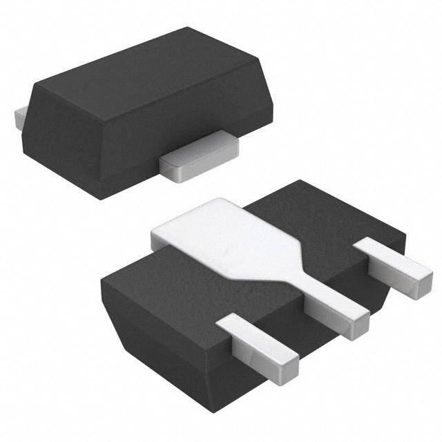
| 描述 | IC GAIN BLOCK AMP SOT89 |
| 产品分类 | RF 放大器 |
| 品牌 | Hittite Microwave Corporation |
| 数据手册 | 点击此处下载产品Datasheet |
| 产品图片 |  |
| P1dB | 13dBm |
| 产品型号 | HMC311ST89E |
| RF类型 | 通用 |
| rohs | 无铅 / 符合限制有害物质指令(RoHS)规范要求 |
| 产品系列 | - |
| 供应商器件封装 | SOT-89 |
| 其它名称 | 1127-1019-2 HMC311ST89ETR |
| 包装 | 带卷 (TR) |
| 噪声系数 | 5dB |
| 增益 | 14.5dB |
| 封装/外壳 | TO-243AA |
| 标准包装 | 500 |
| 测试频率 | - |
| 电压-电源 | 5V |
| 电流-电源 | 74mA |
| 频率 | 0Hz ~ 6GHz |
Datasheet
PDF Datasheet 数据手册内容提取
HMC311ST89 / 311ST89E v04.0517 InGaP HBT GAIN BLOCK MMIC AMPLIFIER, DC - 6 GHz Features Typical Applications The HMC311ST89(E) is ideal for: P1dB Output Power: +15.5 dBm T • Cellular / PCS / 3G Output IP3: +31.5 dBm M • Fixed Wireless & WLAN Gain: 16 dB S • CATV & Cable Modem 50 Ohm I/O’s - K • Microwave Radio Industry Standard SOT89 Package C Included in the HMC-DK001 Designer’s Kit O L B Functional Diagram General Description N The HMC311ST89(E) is a GaAs InGaP Heterojunc- I tion Bipolar Transistor (HBT) Gain Block MMIC SMT A G DC to 6 GHz amplifier. Packaged in an industry standard SOT89E, the amplifier can be used as either & a cascadable 50 Ohm gain stage or to drive the LO of R HMC mixers with up to +16.5 dBm output power. The E HMC311ST89(E) offers 16 dB of gain and an output V IP3 of +31.5 dBm while requiring only 54 mA from a I R +5V supply. The Darlington feedback pair used results D in reduced sensitivity to normal process variations and yields excellent gain stability over temperature - while requiring a minimal number of external bias R components. E I F L Electrical Specifications, Vs= 5V, Rbias= 22 Ohm, T = +25° C I A P M Parameter Min. Typ. Max. Units A DC - 1.0 GHz 14.0 16.0 dB Gain 1.0 - 4.0 GHz 13.0 15.0 dB 4.0 - 6.0 GHz 12.5 14.5 dB DC - 2.0 GHz 0.004 0.007 dB/ °C Gain Variation Over Temperature 2.0 - 4.0 GHz 0.007 0.012 dB/ °C 4.0 - 6.0 GHz 0.012 0.016 dB/ °C DC - 2.0 GHz 8 dB Return Loss Input / Output 2.0 - 5.0 GHz 7 dB 5.0 - 6.0 GHz 8 dB Reverse Isolation DC - 6 GHz 20 dB DC - 2.0 GHz 13.5 15.5 dBm Output Power for 1 dB Compression (P1dB) 2.0 - 4.0 GHz 12.0 15.0 dBm 4.0 - 6.0 GHz 10.0 13.0 dBm DC - 1.0 GHz 31.5 dBm 1.0 - 2.0 GHz 30 dBm Output Third Order Intercept (IP3) 2.0 - 4.0 GHz 27 dBm 4.0 - 6.0 GHz 24 dBm DC - 4 GHz 4.5 Noise Figure dB 4.0 - 6.0 GHz 5 Supply Current (Icq) 55 74 mA Note: Data taken with broadband bias tee on device output. IFnfoorrm patrioicn efu, rndisehleivd ebryy ,A naanlodg tDoe vpicleasc ies boerlideveerds :to A bne aalcocgur aDtee avnidc eresli,a bIlne.c H.,o Owenveer, Tneo chFnoorl opgriyc eW, adye,l iPve.Ory., Banodx t9o1 0pl6a,c Ne oorrwdeoros:d A, nMaAlo g0 2D0e6vi2c-e9s1, 0In6c., 1 rrliiecgsehpntoss neos fi istbh igilrirtday npistae ardtsi esbsuy mt himeadtp m lbicayay At ironenas luoolgrt f oDrtohemev riicwtsei ssu esfo eur.n iStdspPe uerh scaeiofin, ycnn aAopetriaop :ft noe7psrn 8atls inou1cyrb- a jpi3entacfi2rtotei n9tnnogt- ecr4Smhig7auehn0ntpgst0 sepo owfo• fA i ptrnhOtaao:t lueroPdtng nth esoD ootrei crnv oeoiec.tn heN:les io1r.n -e8 OPa0ht0n owe-nA TweNe: wc7Ah8.Lan1Oon-3laoG2lgo9-yDg- 4W.7ca0oy0m, •P .OOr.d Beor xo n9l1in0e6 ,a Nt worwwwoo.adn, aMloAg .0c2o0m62-9106 Trademarks and registered trademarks are the property of their respective owners. Application Support: Phone: 1-800-ANALOG-D
HMC311ST89 / 311ST89E v04.0517 InGaP HBT GAIN BLOCK MMIC AMPLIFIER, DC - 6 GHz Broadband Gain & Return Loss Gain vs. Temperature 20 20 15 18 T 10 16 M B) RESPONSE (d -505 GAIN (dB) 111024 K - S -10 8 C -15 6 O -20 4 L 0 1 2 3 4 5 6 7 8 9 0 1 2 3 4 5 6 7 8 B FREQUENCY (GHz) FREQUENCY (GHz) N +25 C +85 C -40 C S21 S11 S22 I A G Input Return Loss vs. Temperature Output Return Loss vs. Temperature & 0 0 R E B) -5 B) -5 V S (d S (d I S S R O O N L-10 N L-10 D R R U U T T RE-15 RE-15 - R E -20 -20 I 0 1 2 3 4 5 6 7 8 0 1 2 3 4 5 6 7 8 F FREQUENCY (GHz) FREQUENCY (GHz) L I P +25 C +85 C -40 C +25 C +85 C -40 C M A Reverse Isolation vs. Temperature Noise Figure vs. Temperature 0 10 dB) -5 8 ATION (-10 RE (dB) 6 L U O G SE IS-15 SE FI 4 VER NOI RE-20 2 -25 0 0 1 2 3 4 5 6 7 8 1 2 3 4 5 6 7 8 FREQUENCY (GHz) FREQUENCY (GHz) +25 C +85 C -40 C +25 C +85 C -40 C For price, delivery, and to place orders: Analog Devices, Inc., One Technology Way, P.O. Box 9106, Norwood, MA 02062-9106 Phone: 781-329-4700 • Order online at www.analog.com 2 Application Support: Phone: 1-800-ANALOG-D
HMC311ST89 / 311ST89E v04.0517 InGaP HBT GAIN BLOCK MMIC AMPLIFIER, DC - 6 GHz P1dB vs. Temperature Psat vs. Temperature 18 18 T 16 16 M 14 14 S dBm) 12 Bm) 12 - P1dB ( 10 Psat (d 10 K 8 8 C O 6 6 L 4 4 B 0 1 2 3 4 5 6 7 8 0 1 2 3 4 5 6 7 8 FREQUENCY (GHz) FREQUENCY (GHz) N +25 C +85 C -40 C I +25 C +85 C -40 C A G & Power Compression @ 1 GHz Power Compression @ 6 GHz 18 18 R RIVE N (dB), PAE (%) 111180246 N (dB), PAE (%) 111180246 D GAI 6 GAI 6 m), 4 m), 4 R - Pout (dB 02 Pout (dB 02 E -2 -2 I -4 -4 F -20 -18 -16 -14 -12 -10 -8 -6 -4 -2 0 2 4 6 -20 -18 -16 -14 -12 -10 -8 -6 -4 -2 0 2 4 6 L INPUT POWER (dBm) INPUT POWER (dBm) I P Pout Gain PAE Pout Gain PAE M A Gain, Power, OIP3 & Supply Current vs. Output IP3 vs. Temperature Supply Voltage @ 1 GHz 34 m) 40 80 B 30 3 (d 35 70 P 26 m), I 30 60 IP3 (dBm) 1282 Bm), Psat (dB 2205 4500 Icq (mA) d B ( 15 30 14 1d B), P 10 20 10 d 0 1 2 3 4 5 6 7 8 N ( 5 10 FREQUENCY (GHz) GAI 4.5 4.75 5 5.25 5.5 Vs (Vdc) +25 C +85 C -40 C GP1adinB PIPs3at Icq For price, delivery, and to place orders: Analog Devices, Inc., One Technology Way, P.O. Box 9106, Norwood, MA 02062-9106 Phone: 781-329-4700 • Order online at www.analog.com 3 Application Support: Phone: 1-800-ANALOG-D
HMC311ST89 / 311ST89E v04.0517 InGaP HBT GAIN BLOCK MMIC AMPLIFIER, DC - 6 GHz Absolute Maximum Ratings Collector Bias Voltage (Vcc) +7V ELECTROSTATIC SENSITIVE DEVICE RF Input Power (RFIN)(Vcc = +3.9V) +10 dBm T Junction Temperature 150 °C OBSERVE HANDLING PRECAUTIONS M Continuous Pdiss (T = 85 °C) S 0.34 W (derate 5.21 mW/°C above 85 °C) - Thermal Resistance 191 °C/W K (junction to lead) C Storage Temperature -65 to +150 °C O Operating Temperature -40 to +85 °C L Class1A, ESD Sensitivity (HBM) B Passed 250V N I A Outline Drawing G & R E V I R D - R E I F L I P M NOTES: A 1. PACKAGE BODY MATERIAL: MOLDING COMPOUND MP-180S OR EQUIVALENT. 2. LEAD MATERIAL: Cu w/ Ag SPOT PLATING. 3. LEAD PLATING: 100% MATTE TIN. 4. DIMENSIONS ARE IN INCHES [MILLIMETERS] 5. DIMENSION DOES NOT INCLUDE MOLDFLASH OF 0.15mm PER SIDE. 6. DIMENSION DOES NOT INCLUDE MOLDFLASH OF 0.25mm PER SIDE. 7. ALL GROUND LEADS MUST BE SOLDERED TO PCB RF GROUND. Package Information Part Number Package Body Material Lead Finish MSL Rating Package Marking [3] HMC311ST89 Low Stress Injection Molded Plastic Sn/Pb Solder MSL1 [1] 311 XXXX HMC311ST89E RoHS-compliant Low Stress Injection Molded Plastic 100% matte Sn MSL1 [2] H311 XXXX [1] Max peak reflow temperature of 235 °C [2] Max peak reflow temperature of 260 °C [3] 4-Digit lot number XXXX For price, delivery, and to place orders: Analog Devices, Inc., One Technology Way, P.O. Box 9106, Norwood, MA 02062-9106 Phone: 781-329-4700 • Order online at www.analog.com 4 Application Support: Phone: 1-800-ANALOG-D
HMC311ST89 / 311ST89E v04.0517 InGaP HBT GAIN BLOCK MMIC AMPLIFIER, DC - 6 GHz Pin Descriptions Pin Number Function Description Interface Schematic T M This pin is DC coupled. S 1 RFIN An off chip DC blocking capacitor is required. - K C O 3 RFOUT RF output and DC Bias for the output stage. L B N These pins and package bottom must be connected to RF/ 2, 4 GND I DC ground. A G & R E V Application Circuit I R D - R E I F L I P M A Note: 1. Select Rbias to achieve Icq using equation below, Rbias > 22 Ohm. 2. External blocking capacitors are required on RFIN and RFOUT. Icq = Vs - 3.8 Rbias Recommended Component Values Frequency (MHz) Component 50 900 1900 2200 2400 3500 5200 5800 L1 270 nH 56 nH 18 nH 18 nH 15 nH 8.2 nH 3.3 nH 3.3 nH C1, C2 0.01 µF 100 pF 100 pF 100 pF 100 pF 100 pF 100 pF 100 pF For price, delivery, and to place orders: Analog Devices, Inc., One Technology Way, P.O. Box 9106, Norwood, MA 02062-9106 Phone: 781-329-4700 • Order online at www.analog.com 5 Application Support: Phone: 1-800-ANALOG-D
HMC311ST89 / 311ST89E v04.0517 InGaP HBT GAIN BLOCK MMIC AMPLIFIER, DC - 6 GHz Evaluation PCB T M S - K C O L B N I A G & R E V I R D - R E I F L I P M A List of Materials for Evaluation PCB 108313 [1] The circuit board used in the final application Item Description should use RF circuit design techniques. Signal J1 - J2 PCB Mount SMA Connector lines should have 50 Ohm impedance while the J3 - J4 DC Pin package ground leads and package bottom should C1, C2 Capacitor, 0402 Pkg. be connected directly to the ground plane similar to C3 100 pF Capacitor, 0402 Pkg. that shown. A sufficient number of via holes should C4 1000 pF Capacitor, 0603 Pkg. be used to connect the top and bottom ground C5 2.2 µF Capacitor, Tantalum planes. The evaluation board should be mounted to R1 Resistor, 0805 Pkg. an appropriate heat sink. The evaluation circuit board L1 Inductor, 0603 Pkg. shown is available from Analog Devices upon request. U1 HMC311ST89(E) PCB [2] 107368 Evaluation PCB [1] Reference this number when ordering complete evaluation PCB [2] Circuit Board Material: Rogers 4350 For price, delivery, and to place orders: Analog Devices, Inc., One Technology Way, P.O. Box 9106, Norwood, MA 02062-9106 Phone: 781-329-4700 • Order online at www.analog.com 6 Application Support: Phone: 1-800-ANALOG-D