首页 > HMC253QS24E > 详情
 Datasheet下载
- 型号: HMC253QS24E
- 制造商: Hittite
- 库位|库存: xxxx|xxxx
- 要求:
| 数量阶梯 | 香港交货 | 国内含税 |
| +xxxx | $xxxx | ¥xxxx |
查看当月历史价格
查看今年历史价格
产品参数
| 参数 | 数值 |
| 产品目录 | 射频/IF 和 RFID |
| 描述 | IC MMIC GAAS SW SP8T 24QSOP |
| 产品分类 | RF 开关 |
| IIP3 | 43dBm (标准) |
| 品牌 | Hittite Microwave Corporation |
| 数据手册 | 点击此处下载产品Datasheet |
| 产品图片 |  |
| P1dB | 23dBm (标准) IP1dB |
| 产品型号 | HMC253QS24E |
| RF类型 | 通用 |
| rohs | 无铅 / 符合限制有害物质指令(RoHS)规范要求 |
| 产品系列 | - |
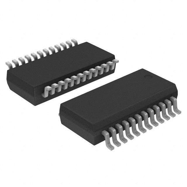
| 供应商器件封装 | 24-QSOP |
| 其它名称 | 1127-1012-6 |
| 包装 | Digi-Reel® |
| 封装/外壳 | 24-SSOP(0.154",3.90mm 宽) |
| 工作温度 | -40°C ~ 85°C |
| 拓扑 | 吸收性 |
| 插损@频率 | 1.8dB @ 2.5GHz |
| 标准包装 | 1 |
| 特性 | - |
| 电压-电源 | 5V |
| 电路 | SP8T |
| 阻抗 | 50 欧姆 |
| 隔离@频率 | 28dB @ 2.5GHz (标准) |
| 频率 -上 | 2.5GHz |
| 频率 -下 | DC |
Datasheet
PDF Datasheet 数据手册内容提取
HMC253QS24 253QS24E / v04.0805 GaAs MMIC SP8T NON-REFLECTIVE SWITCH, DC - 2.5 GHz Typical Applications Features The HMC253QS24 / HMC253QS24E is ideal for Low Insertion Loss (2 GHz): 1.3dB DC - 2.5 GHz applications: Single Positive Supply: Vdd = +5V • CATV/DBS Integrated 3:8 TTL Decoder • CDMA 24 Lead QSOP Package • Cellular/PCS 9 Functional Diagram General Description The HMC253QS24 & HMC253QS24E are low-cost non-refl ective SP8T switches in 24-lead QSOP T packages featuring wideband operation from DC M to 2.5 GHz. The switch offers a single positive bias S and true TTL/CMOS compatibility. A 3:8 decoder is integrated on the switch requiring only 3 control - lines and a positive bias to select each path. The S E HMC253QS24 & HMC253QS24E SP8T will replace H multiple confi gurations of SP4T and SPDT MMIC C switches. T I W S Electrical Specifi cations, T = +25° C, For TTL Control and Vdd = +5V in a 50 Ohm system A Parameter Frequency Min. Typ. Max. Units DC - 1.0 GHz 1.1 1.5 dB Insertion Loss DC - 2.0 GHz 1.3 1.7 dB DC - 2.5 GHz 1.8 2.4 dB DC - 1.0 GHz 32 36 dB Isolation DC - 2.0 GHz 26 30 dB DC - 2.5 GHz 24 28 dB DC - 1.0 GHz 14 18 dB Return Loss “On State” DC - 2.0 GHz 9 12 dB DC - 2.5 GHz 6 8 dB 0.3 - 2.5 GHz 7 10 dB Return Loss (RF1-8) “Off State” 0.5 - 2.5 GHz 10 13 dB Input Power for 1 dB Compression 0.3 - 2.5 GHz 20 23 dBm Input Third Order Intercept 0.3 - 2.5 GHz 40 43 dBm (Two-Tone Input Power = +7 dBm Each Tone) Switching Characteristics 0.3 - 2.5 GHz tRISE, tFALL (10/90% RF) 30 ns tON, tOFF (50% CTL to 10/90% RF) 100 ns Information furnisheFd obry Apnrailcoge D, edviceelsi vise breylie,v eadn tdo bteo a cpcluaractee a nod rrdelieabrlse., Hpowleevaers, eno coFnotra pcritc eH, idtteiltieve rMy, iacnrdo wtoa pvlaec eC oorrdperosr: aAtnioalnog: Devices, Inc., responsibility is assumed by Analog Devices for its use, nor for any infringements of patents or other One Technology Way, P.O. Box 9106, Norwood, MA 02062-9106 9 - 134 rights of third parties tha2t 0ma yA relpsuhlt faro mR itos uasde. ,S pCechifiecaltmionss fsoubrjedct, toM chAan g0e1 w8ith2ou4t nPotihceo. Nnoe : P9h7o8n-e2: 75801--332394-437 0 0F (cid:127)a Ox:r d9e7r o8n-l2in5e 0at- w33w7w3.analog.com license is granted by implication or otherwise under any patent or patent rights of Analog Devices. Trademarks and registered trademarks are the property of their resOpercdtivee orw Onerns.-line at www.hAiptptilticea.tcioonm Support: Phone: 1-800-ANALOG-D
HMC253QS24 / 253QS24E v04.0805 GaAs MMIC SP8T NON-REFLECTIVE SWITCH, DC - 2.5 GHz Insertion Loss Isolation 0 0 -0.5 -10 B) RF6, RF3 d -20 OSS ( -1 N (dB) -30 RTION L-1.5 OLATIO -40 E -2 S INS ++2855 CC I -50 -2.5 -40 C -60 9 RF1, RF2, RF4, RF5, RF7, RF8 -3 -70 0 1 2 3 0 1 2 3 FREQUENCY (GHz) FREQUENCY (GHz) T M S Return Loss - 0 S -5 RRFFCC 1-6 On E RFC 1-6 Off B) H S (d -10 C S O T L -15 URN WI ET -20 R S -25 -30 0 1 2 3 FREQUENCY (GHz) Bias Voltage & Current Truth Table Vdd Range = +5.0 Vdc ± 10% Control Input Signal Path State Vdd Idd (Typ.) Idd (Max.) A B C RFCOM to: (Vdc) (mA) (mA) Low Low Low RF1 +5.0 6.0 9.0 High Low Low RF2 Low High Low RF3 TTL/CMOS Control Voltages High High Low RF4 State Bias Condition Low Low High RF5 Low 0 to +0.8 Vdc @ 5 uA Typ. High Low High RF6 High +2.0 to +5.0 Vdc @ 70 uA Typ. Low High High RF7 High High High RF8 NOTE: DC Blocking capacitors are required at ports RFC and RF1, 2, 3, 4, 5, 6, 7, 8. Information furnisheFd obry Apnrailcoge D, edviceelsi vise breylie,v eadn tdo bteo a cpcluaractee a nod rrdelieabrlse., Hpowleevaers, eno coFnotra pcritc eH, idtteiltieve rMy, iacnrdo wtoa pvlaec eC oorrdperosr: aAtnioalnog: Devices, Inc., responsibility is assumed by Analog Devices for its use, nor for any infringements of patents or other One Technology Way, P.O. Box 9106, Norwood, MA 02062-9106 rights of third parties tha2t 0ma yA relpsuhlt faro mR itos uasde. ,S pCechifiecaltmionss fsoubrjedct, toM chAan g0e1 w8ith2ou4t nPotihceo. Nnoe : P9h7o8n-e2: 75801--332394-437 0 0F (cid:127)a Ox:r d9e7r o8n-l2in5e 0at- w33w7w3.analog.com 9 - 135 license is granted by implication or otherwise under any patent or patent rights of Analog Devices. Trademarks and registered trademarks are the property of their resOpercdtivee orw Onerns.-line at www.hAiptptilticea.tcioonm Support: Phone: 1-800-ANALOG-D
HMC253QS24 / 253QS24E v04.0805 GaAs MMIC SP8T NON-REFLECTIVE SWITCH, DC - 2.5 GHz Absolute Maximum Ratings Bias Voltage Range (Port Vdd) +7.0 Vdc ELECTROSTATIC SENSITIVE DEVICE Control Voltage Range (A, B, C) -0.5V to Vdd +1Vdc OBSERVE HANDLING PRECAUTIONS Storage Temperature -65 to +150 °C Operating Temperature -40 to +85 °C Maximum Input Power +20 dBm (0.05 - 0.5 GHz) Vdd = +5V +24 dBm (0.5 - 2.5 GHz) 9 Outline Drawing T M S - S E H C T I W S NOTES: 1. LEADFRAME MATERIAL: COPPER ALLOY 2. DIMENSIONS ARE IN INCHES [MILLIMETERS]. 3. DIMENSION DOES NOT INCLUDE MOLDFLASH OF 0.15mm PER SIDE. 4. DIMENSION DOES NOT INCLUDE MOLDFLASH OF 0.25mm PER SIDE. 5. ALL GROUND LEADS MUST BE SOLDERED TO PCB RF GROUND. Package Information Part Number Package Body Material Leadframe Plating MSL Rating Package Marking [3] HMC253QS24 Low Stress Injection Molded Plastic Silica Sn/Pb Solder MSL1 [1] HMC253 and Silicon Impregnated XXXX HMC253QS24E RoHS-compliant Low Stress Injection Molded 100% Matte Tin MSL1 [2] HMC253 Plastic Silica and Silicon Impregnated XXXX [1] Max peak refl ow temperature of 235 °C [2] Max peak refl ow temperature of 260 °C [3] 4-Digit lot number XXXX Information furnisheFd obry Apnrailcoge D, edviceelsi vise breylie,v eadn tdo bteo a cpcluaractee a nod rrdelieabrlse., Hpowleevaers, eno coFnotra pcritc eH, idtteiltieve rMy, iacnrdo wtoa pvlaec eC oorrdperosr: aAtnioalnog: Devices, Inc., responsibility is assumed by Analog Devices for its use, nor for any infringements of patents or other One Technology Way, P.O. Box 9106, Norwood, MA 02062-9106 9 - 136 rights of third parties tha2t 0ma yA relpsuhlt faro mR itos uasde. ,S pCechifiecaltmionss fsoubrjedct, toM chAan g0e1 w8ith2ou4t nPotihceo. Nnoe : P9h7o8n-e2: 75801--332394-437 0 0F (cid:127)a Ox:r d9e7r o8n-l2in5e 0at- w33w7w3.analog.com license is granted by implication or otherwise under any patent or patent rights of Analog Devices. Trademarks and registered trademarks are the property of their resOpercdtivee orw Onerns.-line at www.hAiptptilticea.tcioonm Support: Phone: 1-800-ANALOG-D
HMC253QS24 / 253QS24E v04.0805 GaAs MMIC SP8T NON-REFLECTIVE SWITCH, DC - 2.5 GHz Evaluation Circuit Board 9 T M S - S E H C T I W S List of Materials for Evaluation PCB 103706 [1] The circuit board used in the fi nal application should Item Description be generated with proper RF circuit design tech- J1 - J9 PCB Mount SMA Connector niques. Signal lines at the RF ports should have 50 J10 - J14 DC Pin ohm impedance while the package ground leads C1 - C9 100 pF Capacitor, 0402 Pkg. should be connected directly to the ground plane C10 0.01 uF Capacitor, 0603 Pkg. similar to that shown above. A sufficient number of HMC253QS24 / HMC253QS24E U1 SP8T Switch via holes should be used to connect the top and PCB [2] 103704 Eval Board bottom ground planes. The evaluation circuit board [1] Reference this number when ordering complete evaluation PCB shown above is available from Hittite Microwave [2] Circuit Board Material: Rogers 4350 Corporation upon request. Information furnisheFd obry Apnrailcoge D, edviceelsi vise breylie,v eadn tdo bteo a cpcluaractee a nod rrdelieabrlse., Hpowleevaers, eno coFnotra pcritc eH, idtteiltieve rMy, iacnrdo wtoa pvlaec eC oorrdperosr: aAtnioalnog: Devices, Inc., responsibility is assumed by Analog Devices for its use, nor for any infringements of patents or other One Technology Way, P.O. Box 9106, Norwood, MA 02062-9106 rights of third parties tha2t 0ma yA relpsuhlt faro mR itos uasde. ,S pCechifiecaltmionss fsoubrjedct, toM chAan g0e1 w8ith2ou4t nPotihceo. Nnoe : P9h7o8n-e2: 75801--332394-437 0 0F (cid:127)a Ox:r d9e7r o8n-l2in5e 0at- w33w7w3.analog.com 9 - 137 license is granted by implication or otherwise under any patent or patent rights of Analog Devices. Trademarks and registered trademarks are the property of their resOpercdtivee orw Onerns.-line at www.hAiptptilticea.tcioonm Support: Phone: 1-800-ANALOG-D