首页 > HMC232LP4E > 详情
 Datasheet下载
- 型号: HMC232LP4E
- 制造商: Hittite
- 库位|库存: xxxx|xxxx
- 要求:
| 数量阶梯 | 香港交货 | 国内含税 |
| +xxxx | $xxxx | ¥xxxx |
查看当月历史价格
查看今年历史价格
产品参数
| 参数 | 数值 |
| 产品目录 | 射频/IF 和 RFID |
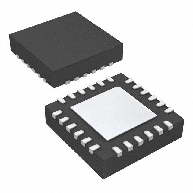
| 描述 | IC GASS MEDFET SW SPDT 24QFN |
| 产品分类 | RF 开关 |
| IIP3 | 50dBm (标准) |
| 品牌 | Hittite Microwave Corporation |
| 数据手册 | 点击此处下载产品Datasheet |
| 产品图片 |  |
| P1dB | 27dBm (标准) IP1dB |
| 产品型号 | HMC232LP4E |
| RF类型 | 通用 |
| rohs | 无铅 / 符合限制有害物质指令(RoHS)规范要求 |
| 产品系列 | - |
| 供应商器件封装 | 24-QFN(4x4) |
| 其它名称 | 1127-1007-1 |
| 包装 | 剪切带 (CT) |
| 封装/外壳 | 24-VFQFN 裸露焊盘 |
| 工作温度 | -40°C ~ 85°C |
| 拓扑 | 吸收性 |
| 插损@频率 | 2.7dB @ 12GHz |
| 标准包装 | 1 |
| 特性 | - |
| 特色产品 | http://www.digikey.cn/product-highlights/zh/new-hmc-series-spdt-switches/53047 |
| 电压-电源 | - |
| 电路 | SPDT |
| 阻抗 | 50 欧姆 |
| 隔离@频率 | 42dB @ 12GHz (标准) |
| 频率 -上 | 12GHz |
| 频率 -下 | DC |
Datasheet
PDF Datasheet 数据手册内容提取
HMC232LP4 232LP4E / v04.0110 GaAs MMIC SPDT NON-REFLECTIVE SWITCH, DC - 12 GHz Typical Applications Features The HMC232LP4(E) is ideal for: Isolation: 60 dB @ 3 GHz 52 dB @ 6 GHz • Telecom Infrastructure Input P1dB: +27 dBm • Microwave Radio & VSAT Insertion Loss: 1.5 dB Typical @ 6 GHz • Military Radios, Radar & ECM Non-Refl ective Design • Test Instrumentation 24 Lead 4x4mm QFN Package: 16mm2 Included in the HMC-DK005 Designer’s Kit Functional Diagram General Description The HMC232LP4(E) is a broadband high isolation non-refl ective GaAs MESFET SPDT switch in a low 11 cost leadless QFN surface mount plastic package. Covering DC to 12 GHz, the switch features >60 dB isolation up to 3 GHz and >42 dB isolation up to 12 GHz. Input P1dB compression is +27 dBm typ- T ical, while input IP3 is +50 dBm. The switch operates M using complementary negative control voltage logic S lines of -5/0V and requires no bias supply. - T D P S - S E Electrical Specifi cations, T = +25° C, With 0/-5V Control, 50 Ohm System A H Parameter Frequency Min. Typ. Max. Units C DC - 3.0 GHz 1.4 1.7 dB T DC - 6.0 GHz 1.5 1.8 dB Insertion Loss I DC - 9.0 GHz 2.0 2.3 dB W DC - 12.0 GHz 2.7 3.1 dB S DC - 3.0 GHz 55 60 dB DC - 6.0 GHz 47 52 dB Isolation DC - 9.0 GHz 40 45 dB DC - 12.0 GHz 37 42 dB DC - 6.0 GHz 18 dB Return Loss “On State” DC - 9.0 GHz 16 dB DC - 12.0 GHz 11 dB Return Loss RF1, RF2 “Off State” DC - 12.0 GHz 14 dB Input Power for 1 dB Compression 0.5 - 12.0 GHz 24 27 dBm Input Third Order Intercept 0.5 - 12.0 GHz 45 50 dBm (Two-Tone Input Power= +7 dBm Each Tone, 1 MHz Tone Separation) Switching Characteristics DC - 12.0 GHz tRISE, tFALL (10/90% RF) 3 ns tON, tOFF (50% CTL to 10/90% RF) 6 ns Information furnisheFd obry Apnrailcoge D, edviceelsi vise breylie,v eadn tdo bteo a cpcluaractee a nod rrdelieabrlse., Hpowleevaers, eno coFnotra pcritc eH, idtteiltieve rMy, iacnrdo wtoa pvlaec eC oorrdperosr: aAtnioalnog: Devices, Inc., responsibility is assumed by Analog Devices for its use, nor for any infringements of patents or other One Technology Way, P.O. Box 9106, Norwood, MA 02062-9106 11 - 54 rights of third parties tha2t 0ma yA relpsuhlt faro mR itos uasde. ,S pCechifiecaltmionss fsoubrjedct, toM chAan g0e1 w8ith2ou4t nPotihceo. Nnoe : P9h7o8n-e2: 75801--332394-437 0 0F (cid:127)a Ox:r d9e7r o8n-l2in5e 0at- w33w7w3.analog.com license is granted by implication or otherwise under any patent or patent rights of Analog Devices. Trademarks and registered trademarks are the property of their resOpercdtivee orw Onerns.-line at www.hAiptptilticea.tcioonm Support: Phone: 1-800-ANALOG-D
HMC232LP4 / 232LP4E v04.0110 GaAs MMIC SPDT NON-REFLECTIVE SWITCH, DC - 12 GHz Insertion Loss Isolation 0 -10 -1 -20 OSS (dB) -2 N (dB) --4300 RRFF12 ON L -3 ATIO -50 ERTI -4 ++2855 CC SOL S -40 C I -60 N I -5 -70 -6 -80 0 1 2 3 4 5 6 7 8 9 10 11 12 13 0 1 2 3 4 5 6 7 8 9 10 11 12 13 FREQUENCY(GH ) Q C (G ) 11 Return Loss 0.1 and 1 dB Input Compression Point 0 30 RFC -5 RF1, RF2 ON T 25 B) RF1, RF2 OFF M d SS ( -10 Bm) S N LO dB (d 20 - UR -15 P1 T RET 15 01. 1d Bd BC oCmopmrpersessiosnio nP oPinotint D -20 P S 10 -25 0 1 2 3 4 5 6 7 8 9 10 11 12 13 0 1 2 3 4 5 6 7 8 9 10 11 12 13 FREQUENCY (GHz) - FREQUENCY(GH ) S E H C Input Third Order Intercept Point T 60 I W 55 S 50 m) dB 45 3 ( IP +25 C 40 +85 C -40 C 35 30 0 1 2 3 4 5 6 7 8 9 10 11 12 13 FREQUENCY(GH ) Information furnisheFd obry Apnrailcoge D, edviceelsi vise breylie,v eadn tdo bteo a cpcluaractee a nod rrdelieabrlse., Hpowleevaers, eno coFnotra pcritc eH, idtteiltieve rMy, iacnrdo wtoa pvlaec eC oorrdperosr: aAtnioalnog: Devices, Inc., responsibility is assumed by Analog Devices for its use, nor for any infringements of patents or other One Technology Way, P.O. Box 9106, Norwood, MA 02062-9106 rights of third parties tha2t 0ma yA relpsuhlt faro mR itos uasde. ,S pCechifiecaltmionss fsoubrjedct, toM chAan g0e1 w8ith2ou4t nPotihceo. Nnoe : P9h7o8n-e2: 75801--332394-437 0 0F (cid:127)a Ox:r d9e7r o8n-l2in5e 0at- w33w7w3.analog.com 11 - 55 license is granted by implication or otherwise under any patent or patent rights of Analog Devices. Trademarks and registered trademarks are the property of their resOpercdtivee orw Onerns.-line at www.hAiptptilticea.tcioonm Support: Phone: 1-800-ANALOG-D
HMC232LP4 / 232LP4E v04.0110 GaAs MMIC SPDT NON-REFLECTIVE SWITCH, DC - 12 GHz Absolute Maximum Ratings Control Voltages RF Input Power (Vctl = -5V) State Bias Condition +30 dBm (@ +50 °C) (0.5 - 12 GHz) Low 0 to -0.2V @ 10 uA Max. RF1, RF2 Termination +23.5 dBm High -5V @ 10 uA Typ. to -7V @ 45 uA Typ. (0.5 Vdc) Control Voltage Range (A & B) +1V to -7.5V Channel Temperature 150 °C Truth Table Thermal Resistance (R ) TH 94 °C/W (junction to lead) Control Input Signal Path State Storage Temperature -65 to +150 °C A B RFC to RF1 RFC to RF2 Operating Temperature -40 to +85 °C High Low ON OFF ESD Sensitivity (HBM) Class 1A Low High OFF ON Caution: Do not “Hot Switch” power levels greater than +27 dBm (Vctl = 0/-5 Vdc). ELECTROSTATIC SENSITIVE DEVICE OBSERVE HANDLING PRECAUTIONS 11 Outline Drawing T M S - T D P S - S E H C NOTES: T 1. LEADFRAME MATERIAL: COPPER ALLOY I 2. DIMENSIONS ARE IN INCHES [MILLIMETERS] W 3. LEAD SPACING TOLERANCE IS NON-CUMULATIVE. 4. PAD BURR LENGTH SHALL BE 0.15mm MAXIMUM. S PAD BURR HEIGHT SHALL BE 0.05mm MAXIMUM. 5. PACKAGE WARP SHALL NOT EXCEED 0.05mm. 6. ALL GROUND LEADS AND GROUND PADDLE MUST BE SOLDERED TO PCB RF GROUND. 7. REFER TO HITTITE APPLICATION NOTE FOR SUGGESTED Package Information LAND PATTERN. Part Number Package Body Material Lead Finish MSL Rating Package Marking [3] HMC232LP4 Low Stress Injection Molded Plastic Sn/Pb Solder MSL1 [1] H232 XXXX HMC232LP4E RoHS-compliant Low Stress Injection Molded Plastic 100% matte Sn MSL1 [2] H232 XXXX [1] Max peak refl ow temperature of 235 °C [2] Max peak refl ow temperature of 260 °C [3] 4-Digit lot number XXXX Information furnisheFd obry Apnrailcoge D, edviceelsi vise breylie,v eadn tdo bteo a cpcluaractee a nod rrdelieabrlse., Hpowleevaers, eno coFnotra pcritc eH, idtteiltieve rMy, iacnrdo wtoa pvlaec eC oorrdperosr: aAtnioalnog: Devices, Inc., responsibility is assumed by Analog Devices for its use, nor for any infringements of patents or other One Technology Way, P.O. Box 9106, Norwood, MA 02062-9106 11 - 56 rights of third parties tha2t 0ma yA relpsuhlt faro mR itos uasde. ,S pCechifiecaltmionss fsoubrjedct, toM chAan g0e1 w8ith2ou4t nPotihceo. Nnoe : P9h7o8n-e2: 75801--332394-437 0 0F (cid:127)a Ox:r d9e7r o8n-l2in5e 0at- w33w7w3.analog.com license is granted by implication or otherwise under any patent or patent rights of Analog Devices. Trademarks and registered trademarks are the property of their resOpercdtivee orw Onerns.-line at www.hAiptptilticea.tcioonm Support: Phone: 1-800-ANALOG-D
HMC232LP4 / 232LP4E v04.0110 GaAs MMIC SPDT NON-REFLECTIVE SWITCH, DC - 12 GHz Suggested Driver Circuit 11 Pin Descriptions T M Pin Number Function Description Interface Schematic 1, 2, 6, 7, 11, The pins are not connected internally; however, all data shown S 12, 13, 14, 17, N/C herein was measured with these pins connected to RF/DC 18, 19, 20, 24 ground externally. - T 3, 5, 8, Package bottom must also D GND 10, 21, 23 be connected to PCB RF ground. P S This pin is DC coupled and matched to 50 Ohm. Blocking 4, 9, 22 RFC, RF1, RF2 capacitors are required if RF line potential is not equal to 0V. - S 15 B See truth table and control voltage table. E H 16 A See truth table and control voltage table. C T I W S Information furnisheFd obry Apnrailcoge D, edviceelsi vise breylie,v eadn tdo bteo a cpcluaractee a nod rrdelieabrlse., Hpowleevaers, eno coFnotra pcritc eH, idtteiltieve rMy, iacnrdo wtoa pvlaec eC oorrdperosr: aAtnioalnog: Devices, Inc., responsibility is assumed by Analog Devices for its use, nor for any infringements of patents or other One Technology Way, P.O. Box 9106, Norwood, MA 02062-9106 rights of third parties tha2t 0ma yA relpsuhlt faro mR itos uasde. ,S pCechifiecaltmionss fsoubrjedct, toM chAan g0e1 w8ith2ou4t nPotihceo. Nnoe : P9h7o8n-e2: 75801--332394-437 0 0F (cid:127)a Ox:r d9e7r o8n-l2in5e 0at- w33w7w3.analog.com 11 - 57 license is granted by implication or otherwise under any patent or patent rights of Analog Devices. Trademarks and registered trademarks are the property of their resOpercdtivee orw Onerns.-line at www.hAiptptilticea.tcioonm Support: Phone: 1-800-ANALOG-D
HMC232LP4 / 232LP4E v04.0110 GaAs MMIC SPDT NON-REFLECTIVE SWITCH, DC - 12 GHz Evaluation PCB 11 T M S - T D P S - S E H C List of Materials for Evaluation PCB 107723 [1] T The circuit board used in the application should I Item Description W be generated with proper RF circuit design tech- J1 - J3 PCB Mount SMA RF Connector S niques. Signal lines at the RF port should have J4 - J6 DC Pin 50 Ohm impedance and the package ground leads C1, C2 100 pF Capacitor, 0603 Pkg. and package bottom should be connected directly U1 HMC232LP4 / HMC232LP4E SPDT Switch to the ground plane similar to that shown above. The PCB [2] 107602 Evaluation PCB evaluation circuit board shown above is available [1] Reference this number when ordering complete evaluation PCB from Hittite Microwave Corporation upon request. [2] Circuit Board Material: Rogers 4350 Information furnisheFd obry Apnrailcoge D, edviceelsi vise breylie,v eadn tdo bteo a cpcluaractee a nod rrdelieabrlse., Hpowleevaers, eno coFnotra pcritc eH, idtteiltieve rMy, iacnrdo wtoa pvlaec eC oorrdperosr: aAtnioalnog: Devices, Inc., responsibility is assumed by Analog Devices for its use, nor for any infringements of patents or other One Technology Way, P.O. Box 9106, Norwood, MA 02062-9106 11 - 58 rights of third parties tha2t 0ma yA relpsuhlt faro mR itos uasde. ,S pCechifiecaltmionss fsoubrjedct, toM chAan g0e1 w8ith2ou4t nPotihceo. Nnoe : P9h7o8n-e2: 75801--332394-437 0 0F (cid:127)a Ox:r d9e7r o8n-l2in5e 0at- w33w7w3.analog.com license is granted by implication or otherwise under any patent or patent rights of Analog Devices. Trademarks and registered trademarks are the property of their resOpercdtivee orw Onerns.-line at www.hAiptptilticea.tcioonm Support: Phone: 1-800-ANALOG-D
HMC232LP4 / 232LP4E v04.0110 GaAs MMIC SPDT NON-REFLECTIVE SWITCH, DC - 12 GHz Notes: 11 T M S - T D P S - S E H C T I W S Information furnisheFd obry Apnrailcoge D, edviceelsi vise breylie,v eadn tdo bteo a cpcluaractee a nod rrdelieabrlse., Hpowleevaers, eno coFnotra pcritc eH, idtteiltieve rMy, iacnrdo wtoa pvlaec eC oorrdperosr: aAtnioalnog: Devices, Inc., responsibility is assumed by Analog Devices for its use, nor for any infringements of patents or other One Technology Way, P.O. Box 9106, Norwood, MA 02062-9106 rights of third parties tha2t 0ma yA relpsuhlt faro mR itos uasde. ,S pCechifiecaltmionss fsoubrjedct, toM chAan g0e1 w8ith2ou4t nPotihceo. Nnoe : P9h7o8n-e2: 75801--332394-437 0 0F (cid:127)a Ox:r d9e7r o8n-l2in5e 0at- w33w7w3.analog.com 11 - 59 license is granted by implication or otherwise under any patent or patent rights of Analog Devices. Trademarks and registered trademarks are the property of their resOpercdtivee orw Onerns.-line at www.hAiptptilticea.tcioonm Support: Phone: 1-800-ANALOG-D