首页 > HMC213AMS8E > 详情
 Datasheet下载
- 型号: HMC213AMS8E
- 制造商: Hittite
- 库位|库存: xxxx|xxxx
- 要求:
| 数量阶梯 | 香港交货 | 国内含税 |
| +xxxx | $xxxx | ¥xxxx |
查看当月历史价格
查看今年历史价格
产品参数
| 参数 | 数值 |
| 产品目录 | 射频/IF 和 RFID |
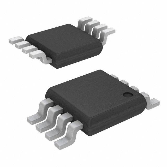
| 描述 | IC MIXER 1.5-4.5GHZ 8MSOP |
| 产品分类 | RF 混频器 |
| 品牌 | Hittite Microwave Corporation |
| 数据手册 | 点击此处下载产品Datasheet |
| 产品图片 |  |
| 产品型号 | HMC213AMS8E |
| RF类型 | 通用 |
| rohs | 无铅 / 符合限制有害物质指令(RoHS)规范要求 |
| 产品系列 | - |
| 供应商器件封装 | 8-MSOP |
| 其它名称 | 1127-1003-6 |
| 包装 | Digi-Reel® |
| 噪声系数 | 8.5dB |
| 增益 | - |
| 封装/外壳 | 8-TSSOP,8-MSOP(0.118",3.00mm 宽) |
| 标准包装 | 1 |
| 混频器数 | 1 |
| 电压-电源 | - |
| 电流-电源 | - |
| 辅助属性 | 升/降频器 |
| 频率 | 1.5GHz ~ 4.5GHz |
Datasheet
PDF Datasheet 数据手册内容提取
HMC213AMS8 213AMS8E / v02.1210 GaAs MMIC SMT Double- bAlAnCeD MIxer, 1.5 - 4.5 GHz Typical Applications Features The HMC213AMs8(e) is ideal for: Ultra small Package: MsOP8 • Base stations Conversion Loss: 8.5 dB 10 • PCMCiA Transceivers LO / rF isolation: 40 dB E • Wireless Local Loop T M T s Functional Diagram General Description - E D The HMC213AMs8(e) is a ultra miniature double- e balanced mixer in 8 lead plastic surface mount C package (MsOP). This passive MMiC mixer is N L constructed of GaAs schottky diodes and novel A planar transformer baluns on the chip. The device can L A be used as an upconverter, downconverter, biphase O B (de)modulator, or phase comparator. The consistent MMiC performance will improve system operation and e L assure regulatory compliance. B S U O D B & e L G O N i electrical Specifications, T = +25° C, As a Function of lo Drive s A - LO = +13 dBm LO = +10 dBm s Parameter iF = 100 MHz iF = 100 MHz Units Min. Typ. Max. Min. Typ. Max. r e Frequency range, rF & LO 1.5 - 4.5 1.7 - 3.6 GHz x Frequency range, iF DC - 1.5 DC - 1.5 GHz i Conversion Loss 8.5 10 9 10.5 dB M Noise Figure (ssB) 8.5 10 9 10.5 dB LO to rF isolation 29 40 32 40 dB LO to iF isolation 27 35 26 35 dB iP3 (input) 16 19 14 18 dBm 1 dB Gain Compression (input) 7 10 5 8 dBm InforFmaotiro np fruircniseh,e dd beyl iAvnealroyg Daenvidce st ois pbelaliecveed otor dbee arcsc:u rHateit taintde reMliaibcler. oHwowaevveer, Cnoo rpFoorr aptriiocen,, d2e0liv Aerlyp, haand R too apdla,c Ce horedlemrss: fAonrdal,o gM DAe v0ic1e8s2, 4Inc., responsibility is assumed by Analog Devices for its use, nor for any infringements of patents or other One Technology Way, P.O. Box 9106, Norwood, MA 02062-9106 10 - 1 rliicgehntss eo fi sth girrda nptaerdti ebsy t himatp mlicaaPyt iorhenso uonlrt ofertoh:m e9r wit7sis 8ues -eu2.n dS5ep0re ca-inf3iyc 3aptia4otne3sn ts ou rb jpeFacttae tnoxt c:r hig9ahn7tgs 8eo wf- 2Aithn5oau0lot g-n 3oDti3ecve7i.c 3eNso . POhrodnee:r 7 O81n-3-l2i9n-e4 7a0t0 w(cid:127) wOrwde.hr oitntliitnee. cato wmww.analog.com Trademarks and registered trademarks arAe tphep plriocpearttyi oof nth eSir urepsppecotivret :o wPnehrso.ne: 978-250-3A3p4p3li c aotrio na Spuppsp@orht: iPtthitoen.ec: o1-m800-ANALOG-D
HMC213AMS8 / 213AMS8E v02.1210 GaAs MMIC SMT Double- bAlAnCeD MIxer, 1.5 - 4.5 GHz Conversion Gain vs. Temperature @ lo = +13 dbm Isolation @ lo = +13 dbm 0 0 RF/IF -10 LO/IF B) LO/RF N GAIN (d -5 ON (dB)-20 E 10 SIO-10 ATI-30 R L E O V S-40 T CON-15 +-4205 CC I T M +85 C -50 s -20 -60 - 1 1.5 2 2.5 3 3.5 4 4.5 5 1 1.5 E2 2.5 3 3.5 4 4.5 5 D FREQUENCY (GHz) FREQUENCY (GHz) e C L N Conversion Gain vs. lo Drive return loss @ lo = +13 dbm A 0 0 L A O B B) N (d -5 dB) -5 e GAI SS ( L CONVERSION --1150 ++ +11915 dddBBBmmm S RETURN LO--1150 LRIFOF DOUB B & -20 -20 1 1.5 2 2.5 3 3.5 4 4.5 5 0 0.5 1 1.5 2 2.5 3 3.5 4 4.5 5 e FREQUENCY (GHz) FREQUENCY (GHz) L O G N IF bandwidth @ lo = +13 dbm P1db vs. Temperature @ lo = +13 dbm i s 0 16 - 15 s B) r d -5 14 N ( e N GAI dBm) 13 x SIO-10 dB ( 12 Mi R 1 E P 11 V N O-15 LO=1.8 GHz, RF=1.9 to 4.9 GHz 10 C LO=4.4 GHz, RF=1.3 to 4.3 GHz -40 C +25 C 9 +85 C -20 8 0 0.5 1 1.5 2 1.5 2 2.5 3 3.5 4 4.5 5 FREQUENCY (GHz) FREQUENCY (GHz) InforFmaotiro np fruircniseh,e dd beyl iAvnealroyg Daenvidce st ois pbelaliecveed otor dbee arcsc:u rHateit taintde reMliaibcler. oHwowaevveer, Cnoo rpFoorr aptriiocen,, d2e0liv Aerlyp, haand R too apdla,c Ce horedlemrss: fAonrdal,o gM DAe v0ic1e8s2, 4Inc., responsibility is assumed by Analog Devices for its use, nor for any infringements of patents or other One Technology Way, P.O. Box 9106, Norwood, MA 02062-9106 rights of third parties that maPy rhesounlt fero:m 9 it7s 8us-e2. S5p0ec-if3ic3ati4on3s s u b jeFcta tox c: h9an7g8e w-2ith5ou0t -n3oti3ce7. 3No POhrodnee:r 7 O81n-3-l2i9n-e4 7a0t0 w(cid:127) wOrwde.hr oitntliitnee. cato wmww.analog.com 10 - 2 license is granted by implication or otherwise under any patent or patent rights of Analog Devices. Trademarks and registered trademarks arAe tphep plriocpearttyi oof nth eSir urepsppecotivret :o wPnehrso.ne: 978-250-3A3p4p3li c aotrio na Spuppsp@orht: iPtthitoen.ec: o1-m800-ANALOG-D
HMC213AMS8 / 213AMS8E v02.1210 GaAs MMIC SMT Double- bAlAnCeD MIxer, 1.5 - 4.5 GHz Input IP3 vs. Input IP3 vs. lo Drive Temperature @ lo = +13 dbm 25 25 10 m) 20 m) 20 B B E d d 3 ( 3 ( P P T I T I U U P +11 dBm P -40C MT IN 15 ++1153 ddBBmm IN 15 T++8255CC s 10 10 - 1.5 2 2.5 3 3.5 4 4.5 5 1.5 2 E2.5 3 3.5 4 4.5 5 D LO FREQUENCY (GHz) LO FREQUENCY (GHz) e C N InpLut IP2 vs. A Input IP2 vs. lo Drive Temperature @ lo = +13 dbm L 64 64 A O B 60 ++1115 ddBBmm 60 +-4805CC +13 dBm +25C e m) 56 m) 56 B B L d d B T IP2 ( 52 S T IP2 ( 52 U U U P P N 48 N 48 O I I D 44 44 B & 40 40 1.5 2 2.5 3 3.5 4 4.5 5 1.5 2 2.5 3 3.5 4 4.5 5 e LO FREQUENCY (GHz) LO FREQUENCY (GHz) L G O N i s - s r e x i M InforFmaotiro np fruircniseh,e dd beyl iAvnealroyg Daenvidce st ois pbelaliecveed otor dbee arcsc:u rHateit taintde reMliaibcler. oHwowaevveer, Cnoo rpFoorr aptriiocen,, d2e0liv Aerlyp, haand R too apdla,c Ce horedlemrss: fAonrdal,o gM DAe v0ic1e8s2, 4Inc., responsibility is assumed by Analog Devices for its use, nor for any infringements of patents or other One Technology Way, P.O. Box 9106, Norwood, MA 02062-9106 10 - 3 rliicgehntss eo fi sth girrda nptaerdti ebsy t himatp mlicaaPyt iorhenso uonlrt ofertoh:m e9r wit7sis 8ues -eu2.n dS5ep0re ca-inf3iyc 3aptia4otne3sn ts ou rb jpeFacttae tnoxt c:r hig9ahn7tgs 8eo wf- 2Aithn5oau0lot g-n 3oDti3ecve7i.c 3eNso . POhrodnee:r 7 O81n-3-l2i9n-e4 7a0t0 w(cid:127) wOrwde.hr oitntliitnee. cato wmww.analog.com Trademarks and registered trademarks arAe tphep plriocpearttyi oof nth eSir urepsppecotivret :o wPnehrso.ne: 978-250-3A3p4p3li c aotrio na Spuppsp@orht: iPtthitoen.ec: o1-m800-ANALOG-D
HMC213AMS8 / 213AMS8E v02.1210 GaAs MMIC SMT Double- bAlAnCeD MIxer, 1.5 - 4.5 GHz Mxn Spurious outputs Harmonics of lo @ rF Port nLO LO Freq. nLO spur mrF 0 1 2 3 4 (GHz) 1 2 3 4 0 xx 12.7 20.8 19.8 76.2 1.5 40 30 62 57 10 1 13.4 0 39.8 38.9 56.2 2.0 38 25 E55 58 2 73.8 78.2 66.5 82.2 68.8 2.5 41 28 34 61 3 93.8 89.2 92.2 82.4 89.0 3.0 41 35 36 61 T 4 >105 >105 >105 >105 >105 3.5 38 45 52 62 T M rF = 3.5 GHz @ -10 dBm 4.0 35 47 55 62 LO = 3.6 GHz @ +13 dBm s 4.5 33 50 65 73 All values in dBc below iF power level (-1rF + 1LO) 5.0 32 52 68 82 - E LO = +13 dBm D Values in dBc below input LO level measured at rF Port. e C L N Absolute Maximum ratings A L rF / iF input +13 dBm O eLeCTrOsTATiC seNsiTiVe DeViCe A LO Drive +27 dBm OBserVe HANDLiNG PreCAUTiONs B Continuous Pdiss (T = 85 °C) 0.69 W (derate 10.6 mW/°C above 85 °C) e Thermal resistance L (Channel to package lead) 93.7 °C/WS B Junction Temperature 150 °C U O storage Temperature -65 to +150 °C Operating Temperature -40 to +85 °C D B & e L O G N i s - s r e x i M InforFmaotiro np fruircniseh,e dd beyl iAvnealroyg Daenvidce st ois pbelaliecveed otor dbee arcsc:u rHateit taintde reMliaibcler. oHwowaevveer, Cnoo rpFoorr aptriiocen,, d2e0liv Aerlyp, haand R too apdla,c Ce horedlemrss: fAonrdal,o gM DAe v0ic1e8s2, 4Inc., responsibility is assumed by Analog Devices for its use, nor for any infringements of patents or other One Technology Way, P.O. Box 9106, Norwood, MA 02062-9106 rights of third parties that maPy rhesounlt fero:m 9 it7s 8us-e2. S5p0ec-if3ic3ati4on3s s u b jeFcta tox c: h9an7g8e w-2ith5ou0t -n3oti3ce7. 3No POhrodnee:r 7 O81n-3-l2i9n-e4 7a0t0 w(cid:127) wOrwde.hr oitntliitnee. cato wmww.analog.com 10 - 4 license is granted by implication or otherwise under any patent or patent rights of Analog Devices. Trademarks and registered trademarks arAe tphep plriocpearttyi oof nth eSir urepsppecotivret :o wPnehrso.ne: 978-250-3A3p4p3li c aotrio na Spuppsp@orht: iPtthitoen.ec: o1-m800-ANALOG-D
HMC213AMS8 / 213AMS8E v02.1210 GaAs MMIC SMT Double- bAlAnCeD MIxer, 1.5 - 4.5 GHz outline Drawing 10 E T M T s - E D e C N L A L A O NOTes: B 1. LeADFrAMe MATeriAL: COPPer ALLOY 2. DiMeNsiONs Are iN iNCHes [MiLLiMeTers]. e 3. DiMeNsiON DOes NOT iNCLUDe MOLDFLAsH OF 0.15mm Per siDe. L 4. DiMeNsiON DOes NOT iNCLUDe MOLDFLAsH OF 0.25mm Per siDe. B 5. ALL GrOUND LeADs MUsT Be sOLDereD TO PCB rF GrOUND. S U O D B & e Package Information L G Part Number O Package Body Material Lead Finish MsL rating Package Marking [3] N HMC213AMs8 Low stress injection Molded Plastic sn/Pb solder MsL1 [1] 213A xxxx i s HMC213AMs8e roHs-compliant Low stress injection Molded Plastic 100% matte sn MsL1 [2] 213A xxxx - s [1] Max peak reflow temperature of 235 °C [2] Max peak reflow temperature of 260 °C r [3] 4-Digit lot number xxxx e x i M InforFmaotiro np fruircniseh,e dd beyl iAvnealroyg Daenvidce st ois pbelaliecveed otor dbee arcsc:u rHateit taintde reMliaibcler. oHwowaevveer, Cnoo rpFoorr aptriiocen,, d2e0liv Aerlyp, haand R too apdla,c Ce horedlemrss: fAonrdal,o gM DAe v0ic1e8s2, 4Inc., responsibility is assumed by Analog Devices for its use, nor for any infringements of patents or other One Technology Way, P.O. Box 9106, Norwood, MA 02062-9106 10 - 5 rliicgehntss eo fi sth girrda nptaerdti ebsy t himatp mlicaaPyt iorhenso uonlrt ofertoh:m e9r wit7sis 8ues -eu2.n dS5ep0re ca-inf3iyc 3aptia4otne3sn ts ou rb jpeFacttae tnoxt c:r hig9ahn7tgs 8eo wf- 2Aithn5oau0lot g-n 3oDti3ecve7i.c 3eNso . POhrodnee:r 7 O81n-3-l2i9n-e4 7a0t0 w(cid:127) wOrwde.hr oitntliitnee. cato wmww.analog.com Trademarks and registered trademarks arAe tphep plriocpearttyi oof nth eSir urepsppecotivret :o wPnehrso.ne: 978-250-3A3p4p3li c aotrio na Spuppsp@orht: iPtthitoen.ec: o1-m800-ANALOG-D
HMC213AMS8 / 213AMS8E v02.1210 GaAs MMIC SMT Double- bAlAnCeD MIxer, 1.5 - 4.5 GHz evaluation PCb 10 E T T M s - E D e C L N A L A O B e L B S U O D B & e L O G N list of Materials for evaluation PCb 103350 [1] i s The circuit board used in the application should item Description - use rF circuit design techniques. signal lines sho- J1 - J3 PCB Mount sMA rF Connector s uld have 50 Ohm impedance while the package U1 HMC213AMs8(e) Mixer r PCB [2] 101650 evaluation Board ground leads and exposed paddle should be con- e nected directly to the ground plane similar to that x [1] reference this number when ordering complete evaluation PCB shown. A sufficient number of via holes should be i [2] Circuit Board Material: rogers 4350 M used to connect the top and bottom ground planes. The evaluation circuit board shown is available from Hittite upon request. InforFmaotiro np fruircniseh,e dd beyl iAvnealroyg Daenvidce st ois pbelaliecveed otor dbee arcsc:u rHateit taintde reMliaibcler. oHwowaevveer, Cnoo rpFoorr aptriiocen,, d2e0liv Aerlyp, haand R too apdla,c Ce horedlemrss: fAonrdal,o gM DAe v0ic1e8s2, 4Inc., responsibility is assumed by Analog Devices for its use, nor for any infringements of patents or other One Technology Way, P.O. Box 9106, Norwood, MA 02062-9106 rights of third parties that maPy rhesounlt fero:m 9 it7s 8us-e2. S5p0ec-if3ic3ati4on3s s u b jeFcta tox c: h9an7g8e w-2ith5ou0t -n3oti3ce7. 3No POhrodnee:r 7 O81n-3-l2i9n-e4 7a0t0 w(cid:127) wOrwde.hr oitntliitnee. cato wmww.analog.com 10 - 6 license is granted by implication or otherwise under any patent or patent rights of Analog Devices. Trademarks and registered trademarks arAe tphep plriocpearttyi oof nth eSir urepsppecotivret :o wPnehrso.ne: 978-250-3A3p4p3li c aotrio na Spuppsp@orht: iPtthitoen.ec: o1-m800-ANALOG-D