首页 > HMC1019LP4E > 详情
 Datasheet下载
- 型号: HMC1019LP4E
- 制造商: Hittite
- 库位|库存: xxxx|xxxx
- 要求:
| 数量阶梯 | 香港交货 | 国内含税 |
| +xxxx | $xxxx | ¥xxxx |
查看当月历史价格
查看今年历史价格
产品参数
| 参数 | 数值 |
| 产品目录 | 射频/IF 和 RFID |
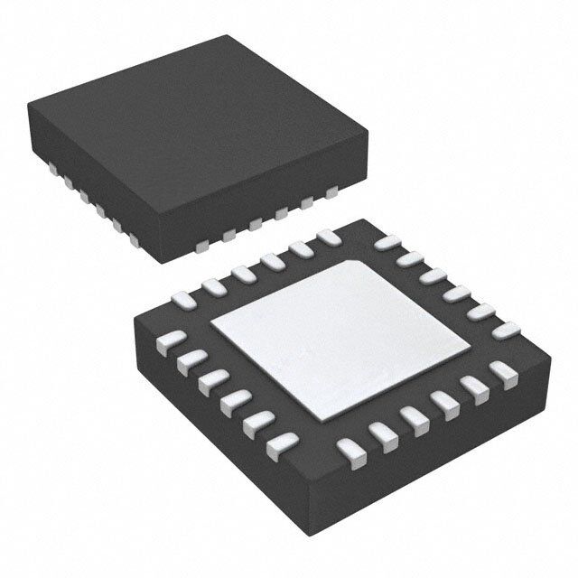
| 描述 | IC DGTL ATTENUATOR 0.5DB 24-QFN |
| 产品分类 | 衰减器 |
| 品牌 | Hittite Microwave Corporation |
| 数据手册 | 点击此处下载产品Datasheet |
| 产品图片 |  |
| 产品型号 | HMC1019LP4E |
| rohs | 无铅 / 符合限制有害物质指令(RoHS)规范要求 |
| 产品系列 | - |
| 其它名称 | 1127-1289 |
| 功率(W) | - |
| 容差 | - |
| 封装/外壳 | 24-VFQFN 裸露焊盘 |
| 标准包装 | 50 |
| 衰减值 | 0.5dB ~ 15.5dB |
| 阻抗 | 50 欧姆 |
| 频率范围 | 100MHz ~ 30GHz |
Datasheet
PDF Datasheet 数据手册内容提取
HMC1019LP4E v00.0911 0.5 dB LSB GaAs MMIC 5-BIT DIGITAL ATTENUATOR, 0.1 - 30 GHz Typical Applications Features the HMC1019lP4e is ideal for: 0.5 dB LSB Steps to 15.5 dB •Fiber Optics & Broadband Telecom TTL/CMOS Compatible, Serial Control t M •Microwave Radio & VSAT Unique Asynchronous Mode Control Allows s •Military Radios, Radar & ECM Immediate Attenuation Level SettingE ±0.5 dB Typical Bit Error - •Space Applications l High Input IP3: +45 dBm •Sensors A t 24 Lead 4x4mm SMT PaTckage: 16mm2 •Test & Measurement Equipment i g i D E Functional Diagram General Description - the HMC1019lP4e is a broadband 5-bit GaAs IC s digital attenuator in a low cost leadless surface r L mount package. Covering 0.1 to 30.0 GHz, the inser- o tion loss is less than 4.0 dB typical. The attenuator t A bit values are 0.5 (LSB), 1, 2, 4, 8 for a total attenu- u O ation of 15.5 dB. Attenuation accuracy is excellent n at ±0.3 dB typical step error with an IIP3 of +45 dBm. e The control interface is CMOS/TTL compatible and t accepts a three wire serial input. The HMC1019LP4E t S features a user selectable power up state and a serial- A output port for cascading other Hittite serial controlled components. B Electrical SpecifiOcations, T = +25° C, With Vdd = Vdd1 = +5V, Vss = -5V A Parameter Frequency (GHz) Min. Typ. Max. Units 0.1 - 18.0 GHz 3.0 4.5 dB Insertion Loss 18.0 - 26.5 GHz 4.0 6.0 dB 26.5 - 30.0 GHz 5.0 6.5 dB Attenuation Range 0.1 - 30.0 GHz 31 dB Return Loss (RF1 & RF2, All Atten. States) 0.1 - 30.0 GHz 12 dB Attenuation Accuracy: (Referenced to Insertion Loss) 0.5 - 7.5 dB States 0.1 - 30.0 GHz ± (0.3 + 6%) of Atten. Setting Max dB 8 - 15.5 dB States 0.1 - 30.0 GHz ± (0.3 + 8%) of Atten. Setting Max dB 0.1 - 0.5 GHz 22 dBm Input Power for 0.1 dB Compression 0.5 - 30.0 GHz 27 dBm Input Third Order Intercept Point 0.1 - 0.5 GHz 42 dBm (Two-Tone Input Power= 0 dBm Each Tone) 0.5 - 30.0 GHz 45 dBm Switching Characteristics 0.1 - 30.0 GHz tRISE, tFALL (10/90% RF) 60 ns tON/tOFF (50% CTL to 10/90% RF) 90 ns idd1 0.1 - 30.0 GHz 2.5 4.5 6.5 mA iss 0.1 - 30.0 GHz -7.0 -5.0 -3.0 mA InfoFrmoart iopn rfiucrneis,h edde blyi vAenraylo ga Dnedvic teos ips lbaelcieeve do rtod beer sac:c Huraittet iatned Mreliiacbrleo. wHoawveeve rC, noo rpoForar tpioricne,, 2d eElilviezrayb, aentdh tDo rpivlaec,e C ohrdeelrms: sAfonardlo,g MDeAv i0ce1s8, 2In4c., responsibility is assumed by Analog Devices for its use, nor for any infringements of patents or other One Technology Way, P.O. Box 9106, Norwood, MA 02062-9106 1 rliicgehntss eo fi sth girrda nptaerdti ebsy t himatp mlicaaPyt iorhenso uonlrt ofertoh:m e9r wit7sis 8ues -eu2.n dS5ep0re ca-inf3iyc 3aptia4otne3sn ts ou rb jpeFacttae tnoxt c:r hig9ahn7tgs 8eo wf- 2Aithn5oau0lot g-n 3oDti3ecve7ic. 3eNso . POhrodnee:r 7 O81n-3-l2i9n-e4 7a0t0 w(cid:127) wOrwde.hr oitntliitnee. cato wmww.analog.com Trademarks and registered trademarks arAe tphep plriocpearttyi oof nth eSir urepsppecotivret :o wPnehrso.ne: 978-250-3A3p4p3li c aotrio na Spuppsp@orht: iPtthitoen.ec: o1-m800-ANALOG-D
HMC1019LP4E v00.0911 0.5 dB LSB GaAs MMIC 5-BIT DIGITAL ATTENUATOR, 0.1 - 30 GHz Normalized Attenuation Insertion Loss vs. Temperature (Only Major States are Shown) 0 0 B) -2 d N ( t B) O -5 ERTION LOSS (d ---864 ZED ATTENUATI-10 E l - sM INS-10 ++2855 CC MALI-15 A -12 -40 C OR T t N i g -14 -20 0 5 10 15 20 25 30 35 40 0 5 10 15 20 25 30 35 40 i D E FREQUENCY (GHz) FREQUENCY (GHz) - s r Input Return Loss OutLput Return Loss o (Only Major States are Shown) (Only Major States are Shown) t 0 0 A O u n B)-10 B)-10 S (d S (d e S S t O O N L-20 S N L-20 t UR UR A T T E E R R -30 -30 B -40 -40 0 5 10 15 20 25 30 35 40 0 5 10 15 20 25 30 35 40 FREQUENCY (GHz) FREQUENCY (GHz) O Bit Error vs. Frequency Bit Error vs. Attenuation State (Only Major States are Shown) 1.2 2 150 G GHHzz 1.5 0.8 18 GHz 15.5 dB 26.5 GHz B) 30 GHz B) 1 d d 8 dB R ( 0.4 R ( 0.5 O O R R R R T E 0 T E 0 BI BI -0.5 -0.4 -1 -0.8 -1.5 0 4 8 12 16 0 5 10 15 20 25 30 35 40 ATTENUATION STATE (dB) FREQUENCY (GHz) InfoFrmoart iopn rfiucrneis,h edde blyi vAenraylo ga Dnedvic teos ips lbaelcieeve do rtod beer sac:c Huraittet iatned Mreliiacbrleo. wHoawveeve rC, noo rpoForar tpioricne,, 2d eElilviezrayb, aentdh tDo rpivlaec,e C ohrdeelrms: sAfonardlo,g MDeAv i0ce1s8, 2In4c., responsibility is assumed by Analog Devices for its use, nor for any infringements of patents or other One Technology Way, P.O. Box 9106, Norwood, MA 02062-9106 rights of third parties that maPy rhesounlt fero:m 9 it7s 8us-e2. S5p0ec-if3ic3ati4on3s s u b jeFcta tox c: h9an7g8e w-2ith5ou0t -n3oti3ce7. 3No POhrodnee:r 7 O81n-3-l2i9n-e4 7a0t0 w(cid:127) wOrwde.hr oitntliitnee. cato wmww.analog.com 2 license is granted by implication or otherwise under any patent or patent rights of Analog Devices. Trademarks and registered trademarks arAe tphep plriocpearttyi oof nth eSir urepsppecotivret :o wPnehrso.ne: 978-250-3A3p4p3li c aotrio na Spuppsp@orht: iPtthitoen.ec: o1-m800-ANALOG-D
HMC1019LP4E v00.0911 0.5 dB LSB GaAs MMIC 5-BIT DIGITAL ATTENUATOR, 0.1 - 30 GHz Relative Phase vs. Frequency Step Attenuation vs. Attenuation State (Only Major States are Shown) 0.1 - 18 GHz 60 1.2 50 1 Mt E (deg) 40 15.5 dB ON (dB) 0.8 s HAS 30 UATI 0.6 E - VE P 20 TEN 0.4 Al ELATI 10 EP AT 0.2 R T 5 GHz t S T 10 GHz 0 0 18 GHz i g -10 -0.2 i 0 5 10 15 20 25 30 35 40 0 4 8 12 16 D E FREQUENCY (GHz) ATTENUATION STATE (dB) - s r Step Attenuation vs. Attenuation State L o 18 - 30 GHz Input Power for 0.1 dB Compression t A 1.4 30 u 1.2 O n dB) 1 26 Atte P ATTENUATION ( 0000....2468 S P0.1dB (dBm) 112482 ++2855 CC E -40 C ST 0 26.5 GHz 10 -0.2 B 30 GHz -0.4 6 0 4 8 12 16 0.01 0.1 1 10 100 ATTENUATION STATE (dB) FREQUENCY (GHz) O Input IP3 vs. Temperature Input IP3 Over Major Attenuation States (Minimum Attenuation State) 60 60 50 50 m) m) B B 3 (d 40 3 (d 40 P P I I +25 C 30 30 +85 C -40 C 20 20 0.01 0.1 1 10 100 0.01 0.1 1 10 100 FREQUENCY (GHz) FREQUENCY (GHz) InfoFrmoart iopn rfiucrneis,h edde blyi vAenraylo ga Dnedvic teos ips lbaelcieeve do rtod beer sac:c Huraittet iatned Mreliiacbrleo. wHoawveeve rC, noo rpoForar tpioricne,, 2d eElilviezrayb, aentdh tDo rpivlaec,e C ohrdeelrms: sAfonardlo,g MDeAv i0ce1s8, 2In4c., responsibility is assumed by Analog Devices for its use, nor for any infringements of patents or other One Technology Way, P.O. Box 9106, Norwood, MA 02062-9106 3 rliicgehntss eo fi sth girrda nptaerdti ebsy t himatp mlicaaPyt iorhenso uonlrt ofertoh:m e9r wit7sis 8ues -eu2.n dS5ep0re ca-inf3iyc 3aptia4otne3sn ts ou rb jpeFacttae tnoxt c:r hig9ahn7tgs 8eo wf- 2Aithn5oau0lot g-n 3oDti3ecve7ic. 3eNso . POhrodnee:r 7 O81n-3-l2i9n-e4 7a0t0 w(cid:127) wOrwde.hr oitntliitnee. cato wmww.analog.com Trademarks and registered trademarks arAe tphep plriocpearttyi oof nth eSir urepsppecotivret :o wPnehrso.ne: 978-250-3A3p4p3li c aotrio na Spuppsp@orht: iPtthitoen.ec: o1-m800-ANALOG-D
HMC1019LP4E v00.0911 0.5 dB LSB GaAs MMIC 5-BIT DIGITAL ATTENUATOR, 0.1 - 30 GHz Serial Control Interface The HMC1019LP4E contains a 3-wire SPI compatible digital interface (SERIN, CLK, LE). The serial control interface is activated when S/A is kept high. The 5-bit serial word must be loaded MSB first as a 6-bit word with the first bit ignored. The positive-edge sensitive CLK and LE requires clean transitions. If mechanical switches are used, sufficient debouncing should be provided. When LE is high, 5-bit data in the serial input register is transferred to the t attenuator. When LE is high CLK is masked to prevent data transition during output loading. M For all modes of operations, the state will stay constant while LE is kept low. E s - l A T t i g i D E - s r L o t A O u n e Serial Mode Truth Table t Control Voltage Input AttSenuation Parameter Typ. t A P4 P3 P2 P1 P0 State Min. serial period, t 100 ns 8 dB 4 dB 2 dB 1 dB 0.5 dB RF1 - RF2 SCK Control set-up time, t 20 ns Cs High High High High High Reference I.L. Control hold-time, t 20 ns B CH High High High High Low 0.5 dB LE setup-time, t 10 ns ln High High High Low High 1 dB Min. LE pulse width, t 10 ns LEW High High Low High High 2 dB Min LE pulse spacing, t 630 ns les High Low HighOHigh High 4 dB Serial clock hold-time from LE, t 10 ns CKN Low High High High High 8 dB Hold Time, t 0 ns PH. Low Low Low Low Low 15.5 dB Latch Enable Minimum Width, t 10 ns len Any combination of the above states will provide an attenuation Setup Time, t 2 ns approximately equal to the sum of the bits selected. Ps Asynchronous Mode The HMC1019LP4E can be switched to an asynchronous mode to change the attenuation state rapidly to one of four predefined states. The logic state of ASM1-ASM2 determines one of the four attenuation states in the asynchronous mode per truth table. The asynchronous mode works either directly or latched. To activate the direct-asynchronous- mode, S/A needs to be at logic low and LE needs to be at logic high. In the direct-asynchronous-mode, any change in the logic state of ASM1-ASM2 directly affects the attenuation state. In the latched-asynchronous-mode, the attenuation state changes per the asynchronous mode truth table when S/A is at logic low and LE is pulsed per the timing diagram. The attenuation stays constant (latched) as long as LE stays low. In the asynchronous mode, the inputs SERIN and CLK do not affect the attenuation state. InfoFrmoart iopn rfiucrneis,h edde blyi vAenraylo ga Dnedvic teos ips lbaelcieeve do rtod beer sac:c Huraittet iatned Mreliiacbrleo. wHoawveeve rC, noo rpoForar tpioricne,, 2d eElilviezrayb, aentdh tDo rpivlaec,e C ohrdeelrms: sAfonardlo,g MDeAv i0ce1s8, 2In4c., responsibility is assumed by Analog Devices for its use, nor for any infringements of patents or other One Technology Way, P.O. Box 9106, Norwood, MA 02062-9106 rights of third parties that maPy rhesounlt fero:m 9 it7s 8us-e2. S5p0ec-if3ic3ati4on3s s u b jeFcta tox c: h9an7g8e w-2ith5ou0t -n3oti3ce7. 3No POhrodnee:r 7 O81n-3-l2i9n-e4 7a0t0 w(cid:127) wOrwde.hr oitntliitnee. cato wmww.analog.com 4 license is granted by implication or otherwise under any patent or patent rights of Analog Devices. Trademarks and registered trademarks arAe tphep plriocpearttyi oof nth eSir urepsppecotivret :o wPnehrso.ne: 978-250-3A3p4p3li c aotrio na Spuppsp@orht: iPtthitoen.ec: o1-m800-ANALOG-D
HMC1019LP4E v00.0911 0.5 dB LSB GaAs MMIC 5-BIT DIGITAL ATTENUATOR, 0.1 - 30 GHz Timing Diagram (Latched Asynchronous Mode) Asynchronous Mode Truth Table AsM1 AsM2 Attenuation State RF1-RF2 High High Reference I.L. t High Low 1.5 dB M Low High 14 dB s Low Low 15.5 dB E - l A t T i g Power-Up States PUP Truth Table i D E If LE is set to logic LOW at power-up, the logic state - PuP Attenuation State of PUP determines the power-up state of the part per s High Reference I.L. PUP truth table. If the LE is set to logic HIGH at power- r Low 15.5 dB L up, the logic state of ASM1-ASM2 determines the o power-up state of the part per truth table for the asyn- Note: The logic state of ASM1-ASM2 determines the t power-up state of the part per truth table for the asyn- A chronous mode. The attenuator latches in the desired chronous mode when LE is high at power-up. u power-up state approximately 200 ms after power-up. O n e t Bias Voltages & Currents Control Voltage t S A Vdd +5V @ 0.2 mA State Bias Condition Vdd1 +5V @ 4.5 mA Low 0 to 0.8V @ 1 µA Vss B-5V @ 5 mA High 2 to 5V @ 1 µA O InfoFrmoart iopn rfiucrneis,h edde blyi vAenraylo ga Dnedvic teos ips lbaelcieeve do rtod beer sac:c Huraittet iatned Mreliiacbrleo. wHoawveeve rC, noo rpoForar tpioricne,, 2d eElilviezrayb, aentdh tDo rpivlaec,e C ohrdeelrms: sAfonardlo,g MDeAv i0ce1s8, 2In4c., responsibility is assumed by Analog Devices for its use, nor for any infringements of patents or other One Technology Way, P.O. Box 9106, Norwood, MA 02062-9106 5 rliicgehntss eo fi sth girrda nptaerdti ebsy t himatp mlicaaPyt iorhenso uonlrt ofertoh:m e9r wit7sis 8ues -eu2.n dS5ep0re ca-inf3iyc 3aptia4otne3sn ts ou rb jpeFacttae tnoxt c:r hig9ahn7tgs 8eo wf- 2Aithn5oau0lot g-n 3oDti3ecve7ic. 3eNso . POhrodnee:r 7 O81n-3-l2i9n-e4 7a0t0 w(cid:127) wOrwde.hr oitntliitnee. cato wmww.analog.com Trademarks and registered trademarks arAe tphep plriocpearttyi oof nth eSir urepsppecotivret :o wPnehrso.ne: 978-250-3A3p4p3li c aotrio na Spuppsp@orht: iPtthitoen.ec: o1-m800-ANALOG-D
HMC1019LP4E v00.0911 0.5 dB LSB GaAs MMIC 5-BIT DIGITAL ATTENUATOR, 0.1 - 30 GHz Absolute Maximum Ratings RF Input Power (0.1 to 30.0 GHz) +27 dBm ELECTROSTATIC SENSITIVE DEVICE Control Voltage (CLK, SERIN, LE, PUP, ASM1, ASM2, S/A) Vdd + 0.5V OBSERVE HANDLING PRECAUTIONS Vdd, Vdd1 +7 Vdc t M Vss -7 Vdc Channel Temperature 150 °C E s Continuous Pdiss (T = 85 oC) (derate 6.8 mW/oC above 85 oC) 0.445 W - l Thermal Resistance 146 °C/W A Storage Temperature -65 to + 150 °C T t i Operating Temperature -40 to +85 °C g ESD Sensitivity (HBM) Class 1A i D E - Outline Drawing s r L o t A O u n e t S t A B O notes: 1. LEADFRAME MATERIAL: COPPER ALLOY 2. DiMensions Are in inCHes [MilliMeters] 3. LEAD SPACING TOLERANCE IS NON-CUMULATIVE. 4. PAD BURR LENGTH SHALL BE 0.15mm MAXIMUM. PAD BURR HEIGHT SHALL BE 0.05mm MAXIMUM. 5. PACKAGE WARP SHALL NOT EXCEED 0.05mm. 6. ALL GROUND LEADS AND GROUND PADDLE MUST BE SOLDERED TO PCB RF GROUND. 7. REFER TO HITTITE APPLICATION NOTE FOR SUGGESTED lAnD PAttern. Package Information Part Number Package Body Material Lead Finish MSL Rating Package Marking [2] HMC1019lP4e RoHS-compliant Low Stress Injection Molded Plastic 100% matte Sn Msl1 [1] H1019 XXXX [1] Max peak reflow temperature of 260 °C [2] 4-Digit lot number XXXX InfoFrmoart iopn rfiucrneis,h edde blyi vAenraylo ga Dnedvic teos ips lbaelcieeve do rtod beer sac:c Huraittet iatned Mreliiacbrleo. wHoawveeve rC, noo rpoForar tpioricne,, 2d eElilviezrayb, aentdh tDo rpivlaec,e C ohrdeelrms: sAfonardlo,g MDeAv i0ce1s8, 2In4c., responsibility is assumed by Analog Devices for its use, nor for any infringements of patents or other One Technology Way, P.O. Box 9106, Norwood, MA 02062-9106 rights of third parties that maPy rhesounlt fero:m 9 it7s 8us-e2. S5p0ec-if3ic3ati4on3s s u b jeFcta tox c: h9an7g8e w-2ith5ou0t -n3oti3ce7. 3No POhrodnee:r 7 O81n-3-l2i9n-e4 7a0t0 w(cid:127) wOrwde.hr oitntliitnee. cato wmww.analog.com 6 license is granted by implication or otherwise under any patent or patent rights of Analog Devices. Trademarks and registered trademarks arAe tphep plriocpearttyi oof nth eSir urepsppecotivret :o wPnehrso.ne: 978-250-3A3p4p3li c aotrio na Spuppsp@orht: iPtthitoen.ec: o1-m800-ANALOG-D
HMC1019LP4E v00.0911 0.5 dB LSB GaAs MMIC 5-BIT DIGITAL ATTENUATOR, 0.1 - 30 GHz Pin Descriptions Pad Number Function Description Interface Schematic t M s 1 serin See truth table, control voltage E 2 le table and timing diagram. - l A t T i g i D 3 Vss Negative Bias -5V E - s r These pins and package bottom 4, 15 gnD L o must be connected to RF/DC ground. t The pins are not connected internally; however, all data A 6-13, 16 n/C shown herein was measured with these pins connected to u RF/DCO ground externally. n These pins are DC coupled and matched to 50 Ohm. Blocking 5, 14 RF1, RF2 e capacitors are required if RF line potential is not equal to 0V. t t S A 17 Vdd1 Positive Bias +5V B 18 Oserout Serial input data delayed by 6 clock cycles. 19 PuP 21 AsM1 See truth table, control voltage 22 AsM2 table and timing diagram. 23 s/A 24 CLK 20 Vdd Serial Controller Bias +5V InfoFrmoart iopn rfiucrneis,h edde blyi vAenraylo ga Dnedvic teos ips lbaelcieeve do rtod beer sac:c Huraittet iatned Mreliiacbrleo. wHoawveeve rC, noo rpoForar tpioricne,, 2d eElilviezrayb, aentdh tDo rpivlaec,e C ohrdeelrms: sAfonardlo,g MDeAv i0ce1s8, 2In4c., responsibility is assumed by Analog Devices for its use, nor for any infringements of patents or other One Technology Way, P.O. Box 9106, Norwood, MA 02062-9106 7 rliicgehntss eo fi sth girrda nptaerdti ebsy t himatp mlicaaPyt iorhenso uonlrt ofertoh:m e9r wit7sis 8ues -eu2.n dS5ep0re ca-inf3iyc 3aptia4otne3sn ts ou rb jpeFacttae tnoxt c:r hig9ahn7tgs 8eo wf- 2Aithn5oau0lot g-n 3oDti3ecve7ic. 3eNso . POhrodnee:r 7 O81n-3-l2i9n-e4 7a0t0 w(cid:127) wOrwde.hr oitntliitnee. cato wmww.analog.com Trademarks and registered trademarks arAe tphep plriocpearttyi oof nth eSir urepsppecotivret :o wPnehrso.ne: 978-250-3A3p4p3li c aotrio na Spuppsp@orht: iPtthitoen.ec: o1-m800-ANALOG-D
HMC1019LP4E v00.0911 0.5 dB LSB GaAs MMIC 5-BIT DIGITAL ATTENUATOR, 0.1 - 30 GHz Application Circuit t M E s - l A T t i g i D E - s r L o t A O u n e t S t A B O InfoFrmoart iopn rfiucrneis,h edde blyi vAenraylo ga Dnedvic teos ips lbaelcieeve do rtod beer sac:c Huraittet iatned Mreliiacbrleo. wHoawveeve rC, noo rpoForar tpioricne,, 2d eElilviezrayb, aentdh tDo rpivlaec,e C ohrdeelrms: sAfonardlo,g MDeAv i0ce1s8, 2In4c., responsibility is assumed by Analog Devices for its use, nor for any infringements of patents or other One Technology Way, P.O. Box 9106, Norwood, MA 02062-9106 rights of third parties that maPy rhesounlt fero:m 9 it7s 8us-e2. S5p0ec-if3ic3ati4on3s s u b jeFcta tox c: h9an7g8e w-2ith5ou0t -n3oti3ce7. 3No POhrodnee:r 7 O81n-3-l2i9n-e4 7a0t0 w(cid:127) wOrwde.hr oitntliitnee. cato wmww.analog.com 8 license is granted by implication or otherwise under any patent or patent rights of Analog Devices. Trademarks and registered trademarks arAe tphep plriocpearttyi oof nth eSir urepsppecotivret :o wPnehrso.ne: 978-250-3A3p4p3li c aotrio na Spuppsp@orht: iPtthitoen.ec: o1-m800-ANALOG-D
HMC1019LP4E v00.0911 0.5 dB LSB GaAs MMIC 5-BIT DIGITAL ATTENUATOR, 0.1 - 30 GHz Evaluation PCB t M s E - l A t T i g i D E - s r L o t A u O n e t t S A B O List of Materials for Evaluation PCB EVAL01-HMC1019LP4E [1] The circuit board used in the application should use Item Description RF circuit design techniques. Signal lines should J1, J2 2.9 mm PC Mount RF Connector have 50 Ohm impedance while the package ground J3, J4, J6 DC Connector leads should be connected directly to the ground J5 2mm DC Header plane similar to that shown. A sufficient number of C1-C3 100 pF Capacitor, 0402 Pkg. via holes should be used to connect the top and C4-C6 1000 pF Capacitor, 0402 Pkg. bottom ground planes. The evaluation circuit board u1 HMC1019LP4E Digital Attenuator shown is available from Hittite upon request. PCB [2] 600-00196-00-2 Evaluation Board [1] Reference this number when ordering complete evaluation PCB [2] Circuit Board Material: Rogers 4350 InfoFrmoart iopn rfiucrneis,h edde blyi vAenraylo ga Dnedvic teos ips lbaelcieeve do rtod beer sac:c Huraittet iatned Mreliiacbrleo. wHoawveeve rC, noo rpoForar tpioricne,, 2d eElilviezrayb, aentdh tDo rpivlaec,e C ohrdeelrms: sAfonardlo,g MDeAv i0ce1s8, 2In4c., responsibility is assumed by Analog Devices for its use, nor for any infringements of patents or other One Technology Way, P.O. Box 9106, Norwood, MA 02062-9106 9 rliicgehntss eo fi sth girrda nptaerdti ebsy t himatp mlicaaPyt iorhenso uonlrt ofertoh:m e9r wit7sis 8ues -eu2.n dS5ep0re ca-inf3iyc 3aptia4otne3sn ts ou rb jpeFacttae tnoxt c:r hig9ahn7tgs 8eo wf- 2Aithn5oau0lot g-n 3oDti3ecve7ic. 3eNso . POhrodnee:r 7 O81n-3-l2i9n-e4 7a0t0 w(cid:127) wOrwde.hr oitntliitnee. cato wmww.analog.com Trademarks and registered trademarks arAe tphep plriocpearttyi oof nth eSir urepsppecotivret :o wPnehrso.ne: 978-250-3A3p4p3li c aotrio na Spuppsp@orht: iPtthitoen.ec: o1-m800-ANALOG-D
HMC1019LP4E v00.0911 0.5 dB LSB GaAs MMIC 5-BIT DIGITAL ATTENUATOR, 0.1 - 30 GHz Notes: t M E s - l A T t i g i D E - s r L o t A O u n e t S t A B O InfoFrmoart iopn rfiucrneis,h edde blyi vAenraylo ga Dnedvic teos ips lbaelcieeve do rtod beer sac:c Huraittet iatned Mreliiacbrleo. wHoawveeve rC, noo rpoForar tpioricne,, 2d eElilviezrayb, aentdh tDo rpivlaec,e C ohrdeelrms: sAfonardlo,g MDeAv i0ce1s8, 2In4c., responsibility is assumed by Analog Devices for its use, nor for any infringements of patents or other One Technology Way, P.O. Box 9106, Norwood, MA 02062-9106 rights of third parties that maPy rhesounlt fero:m 9 it7s 8us-e2. S5p0ec-if3ic3ati4on3s s u b jeFcta tox c: h9an7g8e w-2ith5ou0t -n3oti3ce7. 3No POhrodnee:r 7 O81n-3-l2i9n-e4 7a0t0 w(cid:127) wOrwde.hr oitntliitnee. cato wmww.analog.com 10 license is granted by implication or otherwise under any patent or patent rights of Analog Devices. Trademarks and registered trademarks arAe tphep plriocpearttyi oof nth eSir urepsppecotivret :o wPnehrso.ne: 978-250-3A3p4p3li c aotrio na Spuppsp@orht: iPtthitoen.ec: o1-m800-ANALOG-D