ICGOO在线商城 > 电感器,线圈,扼流圈 > 固定值电感器 > HL021R6BTTR
 Datasheet下载
- 型号: HL021R6BTTR
- 制造商: AVX
- 库位|库存: xxxx|xxxx
- 要求:
| 数量阶梯 | 香港交货 | 国内含税 |
| +xxxx | $xxxx | ¥xxxx |
查看当月历史价格
查看今年历史价格
HL021R6BTTR产品简介:
ICGOO电子元器件商城为您提供HL021R6BTTR由AVX设计生产,在icgoo商城现货销售,并且可以通过原厂、代理商等渠道进行代购。 HL021R6BTTR价格参考。AVXHL021R6BTTR封装/规格:固定值电感器, 1.6nH Unshielded Multilayer Inductor 339mA 137mOhm Max 0402 (1005 Metric) 。您可以下载HL021R6BTTR参考资料、Datasheet数据手册功能说明书,资料中有HL021R6BTTR 详细功能的应用电路图电压和使用方法及教程。
AVX Corporation生产的HL021R6BTTR是一款固定值电感器,属于大电流、小尺寸的功率电感系列,广泛应用于需要高效能电源管理的电子设备中。该电感采用先进的制造工艺,具有低直流电阻(DCR)、高饱和电流和良好的热稳定性,适合在紧凑空间内实现高效的能量转换。

其主要应用场景包括:便携式消费类电子产品,如智能手机、平板电脑和可穿戴设备中的DC-DC转换器,用于提升电源效率并延长电池续航;通信设备中的电源模块,提供稳定的电流滤波与噪声抑制;以及各类嵌入式系统和物联网(IoT)设备中的电压调节模块(VRM),确保微处理器和传感器供电稳定。

此外,HL021R6BTTR也适用于LED驱动电路、小型电源适配器和工业控制设备中的开关电源设计。由于其具备良好的抗电磁干扰(EMI)性能,有助于满足电磁兼容性要求,因此在对信号完整性要求较高的精密电子系统中也有应用。

总体而言,HL021R6BTTR凭借其高可靠性、小体积和优异的电气性能,成为现代高密度、低功耗电子产品中不可或缺的关键元件,特别适用于空间受限但对电源效率和稳定性要求较高的场合。
| 参数 | 数值 |
| 产品目录 | |
| DC电阻(DCR) | 137 毫欧最大 |
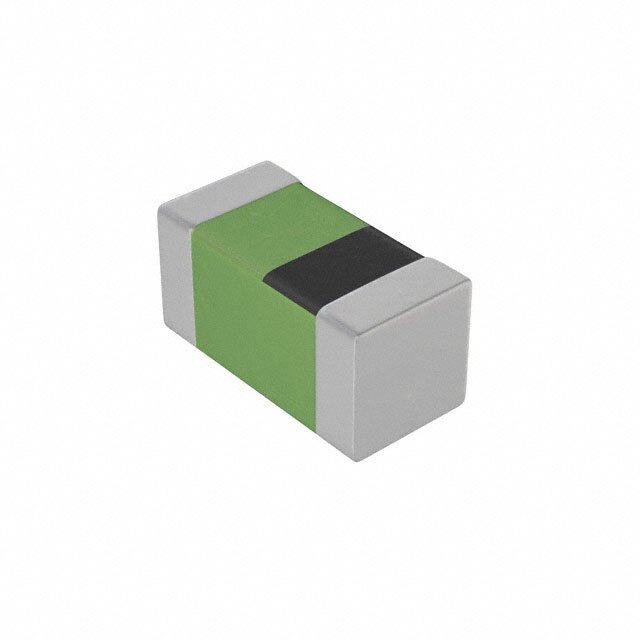
| 描述 | INDUCTOR 1.6NH 339MA 0402固定电感器 1.6nH |
| 产品分类 | |
| 品牌 | AVX Corporation |
| 产品手册 | |
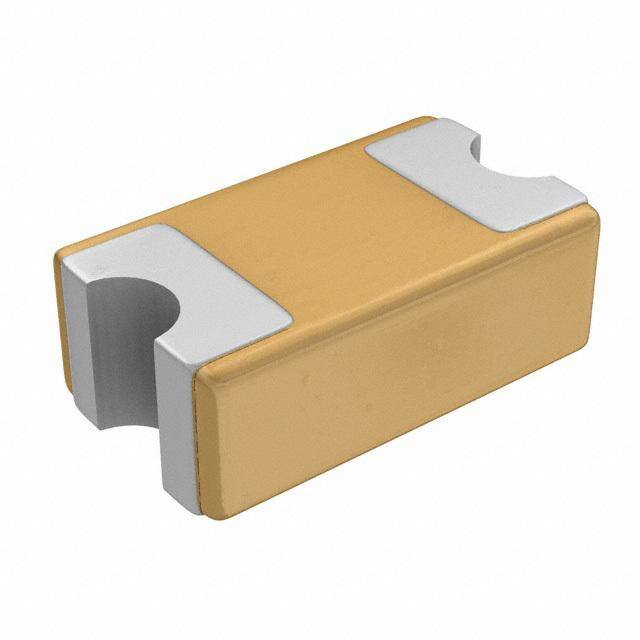
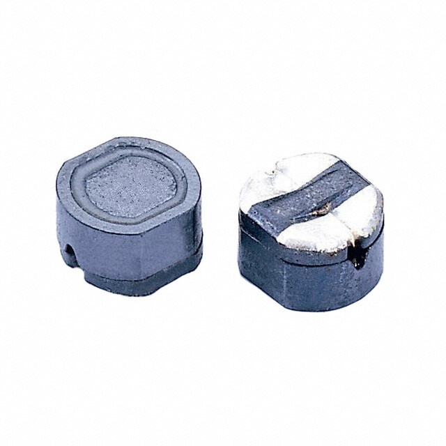
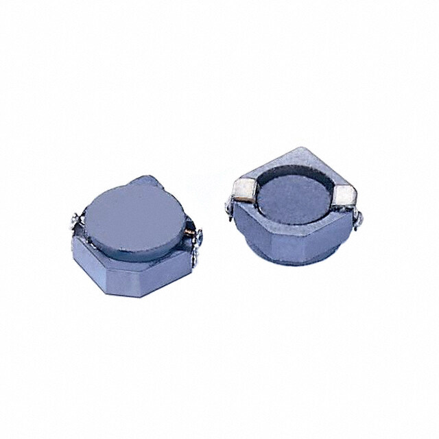
| 产品图片 |
|
| rohs | 符合RoHS无铅 / 符合限制有害物质指令(RoHS)规范要求 |
| 产品系列 | 固定电感器,AVX HL021R6BTTRMLO™ |
| 数据手册 | |
| 产品型号 | HL021R6BTTR |
| Q最小值 | 25 |
| 不同频率时的Q值 | 25 @ 450MHz |
| 产品培训模块 | http://www.digikey.cn/PTM/IndividualPTM.page?site=cn&lang=zhs&ptm=25884 |
| 产品种类 | 固定电感器 |
| 供应商器件封装 | 0402(1005 公制) |
| 其它名称 | 478-6911-2 |
| 包装 | 带卷 (TR) |
| 商标 | AVX |
| 商标名 | MLO |
| 外壳宽度 | 0.58 mm |
| 外壳长度 | 1 mm |
| 外壳高度 | 0.35 mm |
| 大小/尺寸 | 0.039" 长 x 0.023" 宽 (1.00mm x 0.58mm) |
| 安装类型 | 表面贴装 |
| 容差 | ±0.1nH |
| 封装 | Reel |
| 封装/外壳 | 0402(1005 公制) |
| 封装/箱体 | 0402 (1005 metric) |
| 屏蔽 | 无屏蔽 |
| 工作温度 | -55°C ~ 125°C |
| 工作温度范围 | - 55 C to + 125 C |
| 工厂包装数量 | 5000 |
| 最大直流电流 | 339 mA |
| 最大直流电阻 | 137 mOhms |
| 材料-磁芯 | - |
| 标准包装 | 5,000 |
| 特色产品 | http://www.digikey.com/product-highlights/cn/zh/avx-mlo-organic-inductors/1344 |
| 电感 | 1.6nH |
| 电流-饱和值 | - |
| 端接类型 | SMD/SMT |
| 类型 | 多层 |
| 自谐振频率 | 13.4 GHz |
| 频率-测试 | 450MHz |
| 频率-自谐振 | 13.4GHz |
| 额定电流 | 339mA |
| 高度-安装(最大值) | 0.018" (0.45mm) |


PDF Datasheet 数据手册内容提取
MLO® Tight Tolerance Inductors The Multilayer Organic Tight Tolerance Inductor is a low profile organic based inductor that can support mobile communications, satellite applications, GPS, matching networks, and collision avoidance. The MLO® Tight Tolerance Inductor series of components are based on AVX’s patented multilayer organic technology (US patent 6,987,307). MLO® Tight Tolerance Inductors incorporate very low loss organic materials which allow for high Q and high stability over frequency. MLO® Tight Tolerance Inductors are surface mountable and are expansion matched to FR4 printed wiring boards. MLO® Tight Tolerance Inductors utilize fine line high density interconnect technology thereby allowing for tight tolerance control and high repeatability. Reliability testing is performed to JEDEC and mil standards. Finishes are available in RoHS compliant Sn. APPLICATIONS FEATURES SURFACE MOUNT ADVANTAGES • Mobile communications • Tight Tolerance • Satellite Applications • High Frequency • Inherent Low Profile • GPS • High Withstanding Voltage • Excellent Solderability • Collision Avoidance • Low DC Resistance • Low Parasitics • Wireless LAN’s • Surface Mountable • Better Heat Dissipation • 0402 Case Size • Expansion Matched to PCB • RoHS Compliant Finishes • Available in Tape and Reel HOW TO ORDER HL 02 XXX X T TR Style Size Inductance Tolerance Termination Packaging Tight 02 = 0402 Expressed in nH A = ±0.05nH Sn100 5000pcs Tolerance (2 significant digits + number of zeros) B = ±0.1nH T&R for values <10nH, G = ±2% letter R denotes decimal point. Example: 22nH = 220 4.7nH = 4R7 DIMENSIONS QUALITY INSPECTION mm (inches) Finished parts are 100% tested for electrical R parameters and visual characteristics. T B TERMINATION L RoHS compliant Sn finish. W OPERATING TEMPERATURE mm (inches) L W T R B -55ºC to +125ºC 1.00±0.10 0.58±0.075 0.35±0.10 0.125±0.050 0.23±0.0508 (0.040±0.004) (0.023±0.003) (0.014±0.004) (0.005±0.002) (0.0092±0.002) 212 032219
MLO® Tight Tolerance Inductors RECOMMENDED FOOTPRINT mm (inches) Case Size D1 D2 D3 D4 D5 0201 0.85 (0.033) 0.30 (0.012) 0.25 (0.010) 0.30 (0.012) 0.35 (0.014) D2 0402 1.70 (0.067) 0.60 (0.024) 0.50 (0.020) 0.60 (0.024) 0.50 (0.020) 0603 2.30 (0.091) 0.80 (0.031) 0.70 (0.028) 0.80 (0.031) 0.75 (0.030) 0805 3.00 (0.118) 1.00 (0.039) 1.00 (0.039) 1.00 (0.039) 1.25 (0.049) D1 D3 1206 4.00 (0.157) 1.00 (0.039) 2.00 (0.079) 1.00 (0.039) 1.60 (0.063) 1210 4.00 (0.157) 1.00 (0.039) 2.00 (0.079) 1.00 (0.039) 2.50 (0.098) 1808 5.60 (0.220) 1.00 (0.039) 3.60 (0.142) 1.00 (0.039) 2.00 (0.079) D4 1812 5.60 (0.220) 1.00 (0.039) 3.60 (0.142) 1.00 (0.039) 3.00 (0.118) 1825 5.60 (0.220) 1.00 (0.039) 3.60 (0.142) 1.00 (0.039) 6.35 (0.250) 2220 6.60 (0.260) 1.00 (0.039) 4.60 (0.181) 01.00 (0.039) 5.00 (0.197) D5 2225 6.60 (0.260) 1.00 (0.039) 4.60 (0.181) 1.00 (0.039) 6.35 (0.250) Component Pad Design • Pad width equal to component width. It is permissible to decrease this to as low as 85% of compo- Component pads should be designed to achieve good solder filets and minimize component movement nent width but it is not advisable to go below this. during reflow soldering. pad designs are given below for the most common sizes of multilayer ceramic • Pad overlap 0.5mm beneath component. capacitors for both wave and reflow soldering. The basis of these designs is: • Pad extension 0.5mm beyond components for relow and 1.0mm to wave soldering. 0402 ELECTRICAL SPECIFICATIONS Available L (nH) Inductance Tolerance Q Idc max Rdc max SRF min 450MHz A = ±0.05nH, B = ±0.1nH 450MHz (mA) (mΩ) (GHz) G = ±2% 0.8 ±0.05nH, ±0.1nH 15 450 100 7 0.9 ±0.05nH, ±0.1nH 15 450 100 7 1 ±0.05nH, ±0.1nH 15 420 100 7 1.1 ±0.05nH, ±0.1nH 15 410 100 7 1.2 ±0.05nH, ±0.1nH 15 410 110 7 1.3 ±0.05nH, ±0.1nH 15 295 13 7 1.5 ±0.05nH, ±0.1nH 15 295 150 7 1.6 ±0.05nH, ±0.1nH 15 230 150 7 1.8 ±0.05nH, ±0.1nH 15 295 160 7 2 ±0.05nH, ±0.1nH 15 230 18 7 2.2 ±0.05nH, ±0.1nH 15 230 200 7 2.4 ±0.05nH, ±0.1nH 15 230 200 7 2.7 ±0.05nH, ±0.1nH 15 230 250 7 3 ±0.05nH, ±0.1nH 15 200 300 7 3.3 ±0.05nH, ±0.1nH 15 200 340 7 3.6 ±0.05nH, ±0.1nH 15 180 350 7 3.9 ±0.05nH, ±0.1nH 15 180 400 7 4.7 ±0.1nH 15 170 480 7 5.6 ±0.1nH 15 150 500 7 6.8 ±0.1nH 15 140 600 7 8.2 ±0.1nH 15 115 800 6 10 ±2% 15 105 1000 5 12 ±2% 15 95 1100 4 15 ±2% 15 95 1200 4 18 ±2% 15 85 1500 3 22 ±2% 15 75 1900 3 27 ±2% 15 75 2100 3 30 ±2% 15 65 2200 2 32 ±2% 15 65 2200 2 Specifications based on performance of component assembled properly on printed circuit board with 50Ω nominal impedance. 213 050416