ICGOO在线商城 > 集成电路(IC) > 接口 - 驱动器,接收器,收发器 > HIN232ECPZ
 Datasheet下载
- 型号: HIN232ECPZ
- 制造商: Intersil
- 库位|库存: xxxx|xxxx
- 要求:
| 数量阶梯 | 香港交货 | 国内含税 |
| +xxxx | $xxxx | ¥xxxx |
查看当月历史价格
查看今年历史价格
HIN232ECPZ产品简介:
ICGOO电子元器件商城为您提供HIN232ECPZ由Intersil设计生产,在icgoo商城现货销售,并且可以通过原厂、代理商等渠道进行代购。 HIN232ECPZ价格参考。IntersilHIN232ECPZ封装/规格:接口 - 驱动器,接收器,收发器, 全 收发器 2/2 RS232 16-PDIP。您可以下载HIN232ECPZ参考资料、Datasheet数据手册功能说明书,资料中有HIN232ECPZ 详细功能的应用电路图电压和使用方法及教程。
HIN232ECPZ 是瑞萨电子(Renesas Electronics America Inc.)生产的一款RS-232接口芯片,属于接口类中的驱动器/接收器/收发器器件。它主要用于实现TTL/CMOS电平与RS-232电平之间的转换,便于嵌入式系统、工业控制设备等与PC或其他串口设备进行通信。

该芯片的典型应用场景包括:

1. 工业控制系统:用于PLC、传感器、仪表等设备与上位机之间的串口通信。
2. 嵌入式开发板:在ARM、单片机等开发平台中作为串口通信模块,实现与PC调试工具的数据交换。
3. 通信网关设备:用于将不同协议或电平信号进行转换,实现系统间的互连互通。
4. 测试与测量仪器:如示波器、万用表等设备中用于与计算机连接,传输测量数据。
5. POS终端与自动售货机:用于设备内部控制器与外部模块(如打印机、读卡器)之间的串行通信。

HIN232ECPZ具有低功耗、高集成度和工作电压宽等特点,适用于多种需要可靠串口通信的场合。
| 参数 | 数值 |
| 产品目录 | 集成电路 (IC)半导体 |
| 描述 | IC TXRX RS-232 5V ESD 16DIPRS-232接口集成电路 RS232 5V 2D/2R 15KV 0.1UF 16WPDIP COM |
| 产品分类 | |
| 品牌 | Intersil |
| 产品手册 | |
| 产品图片 |
|
| rohs | 符合RoHS无铅 / 符合限制有害物质指令(RoHS)规范要求 |
| 产品系列 | 接口 IC,RS-232接口集成电路,Intersil HIN232ECPZ- |
| 数据手册 | |
| 产品型号 | HIN232ECPZ |
| 产品目录页面 | |
| 产品种类 | RS-232接口集成电路 |
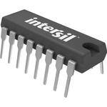
| 供应商器件封装 | 16-PDIP |
| 功能 | Transceiver |
| 包装 | 管件 |
| 协议 | RS232 |
| 双工 | 全 |
| 商标 | Intersil |
| 安装类型 | 通孔 |
| 安装风格 | Through Hole |
| 封装 | Tube |
| 封装/外壳 | 16-DIP(0.300",7.62mm) |
| 封装/箱体 | PDIP-16 |
| 工作温度 | 0°C ~ 70°C |
| 工作温度范围 | + 70 C |
| 工作电源电压 | 5 V |
| 工厂包装数量 | 25 |
| 接收器滞后 | 500mV |
| 接收机数量 | 2 Receiver |
| 数据速率 | 230 kb/s |
| 最大工作温度 | + 70 C |
| 最小工作温度 | 0 C |
| 标准包装 | 25 |
| 激励器数量 | 1 Driver |
| 电压-电源 | 4.5 V ~ 5.5 V |
| 电源电流 | 10 mA |
| 类型 | 收发器 |
| 系列 | HIN232 |
| 驱动器/接收器数 | 2/2 |


PDF Datasheet 数据手册内容提取
DATASHEET HIN202E, HIN206E, HIN207E, HIN208E, HIN211E, HIN213E, HIN232E FN4315 ±15kV, ESD-Protected, +5V Powered, RS-232 Transmitters/Receivers Rev 17.00 September 14, 2015 The HIN202E, HIN206E, HIN207E, HIN208E, HIN211E, Features HIN213E, HIN232E family of RS-232 transmitters/receivers • Pb-Free Plus Anneal Available (RoHS Compliant) interface circuits meet all ElA high-speed RS-232E and V.28 specifications, and are particularly suited for those • High Speed ISDN Compatible . . . . . . . . . . . . . 230kbits/s applications where 12V is not available. A redesigned • ESD Protection for RS-232 I/O Pins to 15kV (IEC61000) transmitter circuit improves data rate and slew rate, which makes this suitable for ISDN and high speed modems. The • Meets All RS-232E and V.28 Specifications transmitter outputs and receiver inputs are protected to • Requires Only 0.1F or Greater External Capacitors 15kV ESD (Electrostatic Discharge). They require a single +5V power supply and feature onboard charge pump voltage • Two Receivers Active in Shutdown Mode (HIN213E) converters which generate +10V and -10V supplies from the • Requires Only Single +5V Power Supply 5V supply. The family of devices offers a wide variety of • Onboard Voltage Doubler/Inverter high-speed RS-232 transmitter/receiver combinations to accommodate various applications (see Selection Table). • Low Power Consumption (Typ) . . . . . . . . . . . . . . . . . 5mA The HIN206E, HIN211E and HIN213E feature a low power • Low Power Shutdown Function (Typ) . . . . . . . . . . . . .1A shutdown mode to conserve energy in battery powered • Three-State TTL/CMOS Receiver Outputs applications. In addition, the HIN213E provides two active receivers in shutdown mode allowing for easy “wakeup” • Multiple Drivers capability. - 10V Output Swing for +5V Input - 300 Power-Off Source Impedance The drivers feature true TTL/CMOS input compatibility, slew - Output Current Limiting rate-limited output, and 300 power-off source impedance. - TTL/CMOS Compatible The receivers can handle up to 30V input, and have a 3k to 7k input impedance. The receivers also feature • Multiple Receivers hysteresis to greatly improve noise rejection. - 30V Input Voltage Range - 3k to 7k Input Impedance - 0.5V Hysteresis to Improve Noise Rejection Applications • Any System Requiring High-Speed RS-232 Communications Port - Computer - Portable, Mainframe, Laptop - Peripheral - Printers and Terminals - Instrumentation, UPS - Modems, ISDN Terminal Adaptors Selection Table NUMBER OF NUMBER OF NUMBER OF NUMBER OF 0.1F LOW POWER RECEIVERS PART POWER SUPPLY RS-232 RS-232 EXTERNAL SHUTDOWN/TTL ACTIVE IN NUMBER VOLTAGE DRIVERS RECEIVERS CAPACITORS THREE-STATE SHUTDOWN HIN202E +5V 2 2 4 Capacitors No/No 0 HIN206E +5V 4 3 4 Capacitors Yes/Yes 0 HIN207E +5V 5 3 4 Capacitors No/No 0 HIN208E +5V 4 4 4 Capacitors No/No 0 HIN211E +5V 4 5 4 Capacitors Yes/Yes 0 HIN213E +5V 4 5 4 Capacitors Yes/Yes 2 HIN232E +5V 2 2 4 Capacitors No/No 0 FN4315 Rev 17.00 Page 1 of 23 September 14, 2015
HIN202E, HIN206E, HIN207E, HIN208E, HIN211E, HIN213E, HIN232E Ordering Information PART NO. TEMP. RANGE PACKAGE (Note 1) PART MARKING (°C) (RoHS Compliant) PKG. DWG. # HIN202ECBZ 202ECBZ 16 Ld SOIC (W) M16.3 HIN202ECBZ-T (Note 2) 202ECBZ 16 Ld SOIC (W) Tape and Reel M16.3 HIN202ECBNZ 202ECBNZ 0 to 70 16 Ld SOIC (N) M16.15 HIN202ECBNZ-T (Note 2) 202ECBNZ 16 Ld SOIC (N) Tape and Reel M16.15 HIN202ECPZ 202ECPZ 16 Ld PDIP* E16.3 HIN202EIBZ 202EIBZ 16 Ld SOIC (W) M16.3 HIN202EIBZ-T (Note 2) 202EIBZ 16 Ld SOIC (W) Tape and Reel M16.3 -40 to 85 HIN202EIBNZ 202EIBNZ 16 Ld SOIC (N) M16.15 HIN202EIBNZ-T (Note 2) 202EIBNZ 16 Ld SOIC (N) Tape and Reel M16.15 HIN206ECBZ HIN206ECBZ 24 Ld SOIC M24.3 0 to 70 HIN206ECBZ-T (Note 2) HIN206ECBZ 24 Ld SOIC Tape and Reel M24.3 HIN206EIAZ HIN206EIAZ 24 Ld SSOP M24.209 -40 to 85 HIN206EIAZ-T (Note 2) HIN206EIAZ 24 Ld SSOP Tape and Reel M24.209 HIN207ECAZ HIN207ECAZ 24 Ld SSOP M24.209 HIN207ECAZ-T (Note 2) HIN207ECAZ 24 Ld SSOP Tape and Reel M24.209 0 to 70 HIN207ECBZ HIN207ECBZ 24 Ld SOIC M24.3 HIN207ECBZ-T (Note 2) HIN207ECBZ 24 Ld SOIC Tape and Reel M24.3 HIN207EIAZ HIN207EIAZ 24 Ld SSOP M24.209 HIN207EIAZ-T (Note 2) HIN207EIAZ 24 Ld SSOP Tape and Reel M24.209 -40 to 85 HIN207EIBZ HIN207EIBZ 24 Ld SOIC M24.3 HIN207EIBZ-T (Note 2) HIN207EIBZ 24 Ld SOIC Tape and Reel M24.3 HIN208ECAZ HIN208ECAZ 24 Ld SSOP M24.209 HIN208ECAZ-T (Note 2) HIN208ECAZ 24 Ld SSOP Tape and Reel M24.209 0 to 70 HIN208ECBZ HIN208ECBZ 24 Ld SOIC M24.3 HIN208ECBZ-T (Note 2) HIN208ECBZ 24 Ld SOIC Tape and Reel M24.3 HIN208EIAZ HIN208EIAZ 24 Ld SSOP M24.209 HIN208EIAZ-T (Note 2) HIN208EIAZ -40 to 85 24 Ld SSOP Tape and Reel M24.209 HIN208EIBZ HIN208EIBZ 24 Ld SOIC M24.3 HIN211ECAZ HIN211ECAZ 28 Ld SSOP M28.209 HIN211ECAZ-T (Note 2) HIN211ECAZ 28 Ld SSOP Tape and Reel M28.209 0 to 70 HIN211ECBZ HIN211ECBZ 28 Ld SOIC M28.3 HIN211ECBZ-T (Note 2) HIN211ECBZ 28 Ld SOIC Tape and Reel M28.3 HIN211EIAZ HIN211EIAZ 28 Ld SSOP M28.209 HIN211EIAZ-T (Note 2) HIN211EIAZ -40 to 85 28 Ld SSOP Tape and Reel M28.209 HIN211EIBZ HIN211EIBZ 28 Ld SOIC M28.3 HIN213ECAZ HIN213ECAZ 28 Ld SSOP M28.209 0 to 70 HIN213ECAZ-T (Note 2) HIN213ECAZ 28 Ld SSOP Tape and Reel M28.209 HIN213EIAZ HIN213EIAZ 28 Ld SSOP M28.209 HIN213EIAZ-T (Note 2) HIN213EIAZ -40 to 85 28 Ld SSOP Tape and Reel M28.209 HIN213EIBZ HIN213EIBZ 28 Ld SOIC M28.3 FN4315 Rev 17.00 Page 2 of 23 September 14, 2015
HIN202E, HIN206E, HIN207E, HIN208E, HIN211E, HIN213E, HIN232E Ordering Information (Continued) PART NO. TEMP. RANGE PACKAGE (Note 1) PART MARKING (°C) (RoHS Compliant) PKG. DWG. # HIN232ECAZ HIN232ECAZ 16 Ld SSOP M16.209 HIN232ECAZ-T (Note 2) HIN232ECAZ 16 Ld SSOP Tape and Reel M16.209 HIN232ECBNZ 232ECBNZ 16 Ld SOIC (N) M16.15 HIN232ECBNZ-T (Note 2) 232ECBNZ 0 to 70 16 Ld SOIC (N) Tape and Reel M16.15 HIN232ECBZ 232ECBZ 16 Ld SOIC (W) M16.3 HIN232ECBZ-T (Note 2) 232ECBZ 16 Ld SOIC (W) Tape and Reel M16.3 HIN232ECPZ HIN232ECPZ 16 Ld PDIP* E16.3 HIN232EIBNZ 232EIBNZ 16 Ld SOIC (N) M16.15 HIN232EIBNZ-T (Note 2) 232EIBNZ 16 Ld SOIC (N) Tape and Reel M16.15 HIN232EIVZ 232EIVZ 16 Ld TSSOP M16.173 (No longer available, recommended replacement: -40 to 85 HIN232ECAZ) HIN232EIVZ-T (Note 2) 232EIVZ 16 Ld TSSOP Tape and Reel M16.173 (No longer available, recommended replacement: HIN232ECAZ-T) *Pb-free PDIPs can be used for through hole wave solder processing only. They are not intended for use in Reflow solder processing applications. NOTES: 1. Intersil Pb-free plus anneal products employ special Pb-free material sets; molding compounds/die attach materials and 100% matte tin plate termination finish, which are RoHS compliant and compatible with both SnPb and Pb-free soldering operations. Intersil Pb-free products are MSL classified at Pb-free peak reflow temperatures that meet or exceed the Pb-free requirements of IPC/JEDEC J STD-020. 2. Please refer to TB347 for details on reel specifications. FN4315 Rev 17.00 Page 3 of 23 September 14, 2015
HIN202E, HIN206E, HIN207E, HIN208E, HIN211E, HIN213E, HIN232E Pinouts HIN202E (PDIP, SOIC) HIN206E (SOIC, SSOP) TOP VIEW TOP VIEW C1+ 1 16 VCC T3OUT 1 24 T4OUT V+ 2 15 GND T1OUT 2 23 R2IN C1- 3 14 T1OUT T2OUT 3 22 R2OUT C2+ 4 13 R1IN R1IN 4 21 SD C2- 5 12 R1OUT R1OUT 5 20 EN T2IN 6 19 T4IN V- 6 11 T1IN T1IN 7 18 T3IN T2OUT 7 10 T2IN GND 8 17 R3OUT R2IN 8 9 R2OUT VCC 9 16 R3IN C1+ 10 15 V- V+ 11 14 C2- C1- 12 13 C2+ +5V +5V 9 10 0.1F C1+ VCC + 16 + 11 0.1F 12 +5V TO 10V V+ 1 VCC 0.1F C1- VOLTAGE DOUBLER 0.1F +3 CC11+- VOLT+A5GV ET OIN 1V0EVRTER V+ 2 + 0.1F +1134 C2+ VOL+T1A0GVE T ION V-1E0RVTER V- 15 4 C2- 0.1F C2+ + 0.1F +5 VOL+T1A0GVE T ION V-1E0RVTER V- 6 7 +5V400k T1 2 C2- 0.1F T1IN T1OUT + +5V T2 T1IN 11 +5V400k T1 14 T1OUT T2IN 6 400k 3 T2OUT +5V T3 +5V T2 18 400k 1 10 400k 7 T3IN T3OUT T2IN T2OUT +5V T4 19 400k 24 12 13 T4IN T4OUT R1OUT R1IN 5 4 R1 5k R1OUT R1IN R1 5k 9 8 R2OUT R2IN 22 23 R2 5k R2OUT R2IN R2 5k GND 15 17 16 R3OUT R3IN 20 R3 5k 21 EN SD GND 8 FN4315 Rev 17.00 Page 4 of 23 September 14, 2015
HIN202E, HIN206E, HIN207E, HIN208E, HIN211E, HIN213E, HIN232E Pinouts (Continued) HIN207E (SOIC, SSOP) HIN208E (SOIC, SSOP) TOP VIEW TOP VIEW T3OUT 1 24 T4OUT T2OUT 1 24 T3OUT T1OUT 2 23 R2IN T1OUT 2 23 R3IN T2OUT 3 22 R2OUT R2IN 3 22 R3OUT R1IN 4 21 T5IN R2OUT 4 21 T4IN R1OUT 5 20 T5OUT T1IN 5 20 T4OUT T2IN 6 19 T4IN R1OUT 6 19 T3IN T1IN 7 18 T3IN R1IN 7 18 T2IN GND 8 17 R3OUT GND 8 17 R4OUT VCC 9 16 R3IN VCC 9 16 R4IN C1+ 10 15 V- C1+ 10 15 V- V+ 11 14 C2- V+ 11 14 C2- C1- 12 13 C2+ C1- 12 13 C2+ +5V +5V 9 9 10 0.1F +10 C1+ VCC 11 +0.1F 0.1F +12 C1+ +5V VTOCC 10V V+ 11 + 0.1F 12 +5V TO 10V V+ C1- VOLTAGE DOUBLER C1- VOLTAGE DOUBLER 13 0.1F +1134 C2+ VOL+T1A0GVE T ION V-1E0RVTER V- 15 0.1F +14 CC22+- VOL+T1A0GVE T ION V-1E0RVTER V- 15 0.1F C2- 0.1F + + +5V T1 7 +5V400k T1 2 T1IN 5 400k 2 T1OUT T1IN T1OUT +5V T2 6 +5V400k T2 3 T2IN 18 400k 1 T2OUT T2IN T2OUT +5V T3 18 +5V400k T3 1 T3IN 19 400k 24 T3OUT T3IN T3OUT +5V T4 19 +5V400k T4 24 T4IN 21 400k 20 T4OUT T4IN T4OUT 6 7 +5V T5 R1OUT R1IN T5IN 21 400k 20 T5OUT R1 5k 5 4 4 3 R1OUT R1IN R2OUT R2IN R1 5k R2 5k 22 23 22 23 R2OUT R2IN R3OUT R3IN R2 5k R3 5k 17 16 17 16 R3OUT R3IN R4OUT R4IN R3 5k R4 5k GND GND 8 8 FN4315 Rev 17.00 Page 5 of 23 September 14, 2015
HIN202E, HIN206E, HIN207E, HIN208E, HIN211E, HIN213E, HIN232E Pinouts (Continued) HIN211E (SOIC, SSOP) HIN213E (SOIC, SSOP) TOP VIEW TOP VIEW T3OUT 1 28 T4OUT T3OUT 1 28 T4OUT T1OUT 2 27 R3IN T1OUT 2 27 R3IN T2OUT 3 26 R3OUT T2OUT 3 26 R3OUT R2IN 4 25 SD R2IN 4 25 SD R2OUT 5 24 EN R2OUT 5 24 EN T2IN 6 23 R4IN T2IN 6 23 R4IN T1IN 7 22 R4OUT T1IN 7 22 R4OUT R1OUT 8 21 T4IN R1OUT 8 21 T4IN R1IN 9 20 T3IN R1IN 9 20 T3IN GND 10 19 R5OUT GND 10 19 R5OUT VCC 11 18 R5IN VCC 11 18 R5IN C1+ 12 17 V- C1+ 12 17 V- V+ 13 16 C2- V+ 13 16 C2- C1- 14 15 C2+ C1- 14 15 C2+ NOTE: R4 and R5 active in shutdown. +5V +5V 11 11 12 0.1F 12 0.1F C1+ VCC + C1+ VCC + + 13 + 13 0.1F 14 +5V TO 10V V+ 0.1F 14 +5V TO 10V V+ C1- VOLTAGE DOUBLER C1- VOLTAGE DOUBLER 15 15 C2+ C2+ 0.1F +16 VOL+T1A0GVE T ION V-1E0RVTER V- 17 0.1F +16 VOL+T1A0GVE T ION V-1E0RVTER V- 17 C2- 0.1F C2- 0.1F + + +5V T1 +5V T1 7 400k 2 7 400k 2 T1IN T1OUT T1IN T1OUT +5V T2 +5V T2 6 400k 3 6 400k 3 T2IN T2OUT T2IN T2OUT +5V T3 +5V T3 20 400k 1 20 400k 1 T3IN T3OUT T3IN T3OUT +5V T4 +5V T4 21 400k 28 21 400k 28 T4IN T4OUT T4IN T4OUT 8 9 8 9 R1OUT R1IN R1OUT R1IN R1 5k R1 5k 5 4 5 4 R2OUT R2IN R2OUT R2IN R2 5k R2 5k 26 27 26 27 R3OUT R3IN R3OUT R3IN R3 5k R3 5k 22 23 22 23 R4OUT R4IN R4OUT R4IN R4 5k R4 5k 19 18 19 18 R5OUT R5IN R5OUT R5IN R5 5k R5 5k 24 25 24 25 EN SD EN SD GND GND 10 10 FN4315 Rev 17.00 Page 6 of 23 September 14, 2015
HIN202E, HIN206E, HIN207E, HIN208E, HIN211E, HIN213E, HIN232E Pinouts (Continued) HIN232E (PDIP, SOIC, SSOP) (TSSOP - NO LONGER AVAILABLE OR SUPPORTED) +5V TOP VIEW 16 1 VCC 0.1F C1+ 1 16 VCC 0.1F +3 C1+ VOLT+A5GV ET OIN 1V0EVRTER V+ 2 + V+ 2 15 GND C1- 4 CC21+- 34 1143 TR11OINUT 0.1F +5 CC22+- VOL+T1A0GVE T ION V-1E0RVTER V- 6 0.1F C2- 5 12 R1OUT + V- 6 11 T1IN 11 +5V400k T1 14 T2OUT 7 10 T2IN T1IN T1OUT R2IN 8 9 R2OUT +5V T2 10 400k 7 T2IN T2OUT 12 13 R1OUT R1IN R1 5k 9 8 R2OUT R2IN R2 5k GND 15 Pin Descriptions PIN FUNCTION VCC Power Supply Input 5V 10%, (5V 5% HIN207E). V+ Internally generated positive supply (+10V nominal). V- Internally generated negative supply (-10V nominal). GND Ground Lead. Connect to 0V. C1+ External capacitor (+ terminal) is connected to this lead. C1- External capacitor (- terminal) is connected to this lead. C2+ External capacitor (+ terminal) is connected to this lead. C2- External capacitor (- terminal) is connected to this lead. TIN Transmitter Inputs. These leads accept TTL/CMOS levels. An internal 400kpull-up resistor to VCC is connected to each lead. TOUT Transmitter Outputs. These are RS-232 levels (nominally 10V). RIN Receiver Inputs. These inputs accept RS-232 input levels. An internal 5kpull-down resistor to GND is connected to each input. ROUT Receiver Outputs. These are TTL/CMOS levels. EN, EN Receiver Enable Input. With EN = 5V (HIN213E EN=0V), the receiver outputs are placed in a high impedance state. SD, SD Shutdown Input. With SD = 5V (HIN213E SD = 0V), the charge pump is disabled, the receiver outputs are in a high impedance state (except R4 and R5 of HIN213E) and the transmitters are shut off. NC No Connect. No connections are made to these leads. FN4315 Rev 17.00 Page 7 of 23 September 14, 2015
HIN202E, HIN206E, HIN207E, HIN208E, HIN211E, HIN213E, HIN232E Absolute Maximum Ratings Thermal Information VCC to Ground. . . . . . . . . . . . . . . . . . . . . .(GND -0.3V) < VCC < 6V Thermal Resistance (Typical, Note 1) JA (°C/W) V+ to Ground. . . . . . . . . . . . . . . . . . . . . . . .(VCC -0.3V) < V+ < 12V 16 Ld SOIC (N) Package. . . . . . . . . . . . . . . . . . . . . 110 V- to Ground . . . . . . . . . . . . . . . . . . . . . . .-12V < V- < (GND +0.3V) 16 Ld SOIC (W) Package. . . . . . . . . . . . . . . . . . . . . 100 Input Voltages 16 Ld SSOP Package . . . . . . . . . . . . . . . . . . . . . . . 155 TIN . . . . . . . . . . . . . . . . . . . . . . . . . . . . .-0.3V < VIN < (V+ +0.3V) 16 Ld TSSOP Package . . . . . . . . . . . . . . . . . . . . . . 145 RIN. . . . . . . . . . . . . . . . . . . . . . . . . . . . . . . . . . . . . . . . . . . . 30V 16 Ld PDIP Package* . . . . . . . . . . . . . . . . . . . . . . . 90 Output Voltages 24 Ld SOIC Package. . . . . . . . . . . . . . . . . . . . . . . . 75 TOUT . . . . . . . . . . . . . . . . . . . .(V- -0.3V) < VTXOUT < (V+ +0.3V) 24 Ld SSOP Package . . . . . . . . . . . . . . . . . . . . . . . 135 ROUT . . . . . . . . . . . . . . . . . (GND -0.3V) < VRXOUT < (V+ +0.3V) 28 Ld SOIC Package. . . . . . . . . . . . . . . . . . . . . . . . 70 Short Circuit Duration 28 Ld SSOP Package . . . . . . . . . . . . . . . . . . . . . . . 100 TOUT . . . . . . . . . . . . . . . . . . . . . . . . . . . . . . . . . . . . . .Continuous Maximum Junction Temperature (Plastic Package) . . . . . . . .150°C ROUT . . . . . . . . . . . . . . . . . . . . . . . . . . . . . . . . . . . . . .Continuous Maximum Storage Temperature Range . . . . . . . . . .-65°C to 150°C ESD Classification. . . . . . . . . . . . . . . . . . . .See Specification Table Maximum Lead Temperature (Soldering 10s). . . . . . . . . . . . .300°C (SOIC and SSOP - Lead Tips Only) Operating Conditions *Pb-free PDIPs can be used for through hole wave solder Temperature Range processing only. They are not intended for use in Reflow solder HIN2XXECX. . . . . . . . . . . . . . . . . . . . . . . . . . . . . . . . 0°C to 70°C processing applications. HIN2XXEIX. . . . . . . . . . . . . . . . . . . . . . . . . . . . . . . .-40°C to 85°C CAUTION: Stresses above those listed in “Absolute Maximum Ratings” may cause permanent damage to the device. This is a stress only rating and operation of the device at these or any other conditions above those indicated in the operational sections of this specification is not implied. NOTE: 3. JA is measured with the component mounted on an evaluation PC board in free air. Electrical Specifications Test Conditions: VCC = +5V 10%, (VCC = +5V 5% HIN207E); C1-C4 = 0.1F; TA = Operating Temperature Range PARAMETER TEST CONDITIONS MIN TYP MAX UNITS SUPPLY CURRENTS Power Supply Current, ICC No Load, HIN202E - 8 15 mA TA = 25°C HIN206E - HIN208E, HIN211E, - 11 20 mA HIN213E HIN232E - 5 10 mA Shutdown Supply Current, ICC(SD) TA = 25°C HIN206E, HIN211E - 1 10 A HIN213E - 15 50 A LOGIC AND TRANSMITTER INPUTS, RECEIVER OUTPUTS Input Logic Low, VlL TIN, EN, SD, EN, SD - - 0.8 V Input Logic High, VlH TIN 2.0 - - V EN, SD, EN, SD 2.4 - - V Transmitter Input Pullup Current, IP TIN = 0V - 15 200 A TTL/CMOS Receiver Output Voltage Low, VOL IOUT = 1.6mA (HIN202E, HIN232E, IOUT = 3.2mA) - 0.1 0.4 V TTL/CMOS Receiver Output Voltage High, VOH IOUT = -1mA 3.5 4.6 - V TTL/CMOS Receiver Output Leakage EN = VCC, EN = 0, 0V < ROUT < VCC - 0.5 10 A RECEIVER INPUTS RS-232 Input Voltage Range, VIN -30 - +30 V Receiver Input Impedance, RIN TA = 25°C, VIN = 3V 3.0 5.0 7.0 k Receiver Input Low Threshold, VIN (H-L) VCC = 5V, Active Mode - 1.2 - V TA = 25°C Shutdown Mode HIN213E R4 and R5 - 1.5 - V Receiver Input High Threshold, VIN (L-H) VCC = 5V, Active Mode - 1.7 2.4 V TA = 25°C Shutdown Mode HIN213E R4 and R5 - 1.5 2.4 V Receiver Input Hysteresis, VHYST VCC = 5V, No Hysteresis in Shutdown Mode 0.2 0.5 1.0 V FN4315 Rev 17.00 Page 8 of 23 September 14, 2015
HIN202E, HIN206E, HIN207E, HIN208E, HIN211E, HIN213E, HIN232E Electrical Specifications Test Conditions: VCC = +5V 10%, (VCC = +5V 5% HIN207E); C1-C4 = 0.1F; TA = Operating Temperature Range (Continued) PARAMETER TEST CONDITIONS MIN TYP MAX UNITS TIMING CHARACTERISTICS Output Enable Time, tEN HIN206E, HIN211E, HIN213E - 600 - ns Output Disable Time, tDIS HIN206E, HIN211E, HIN213E - 200 - ns Transmitter, Receiver Propagation Delay, tPD HIN213E SD = 0V, R4, R5 - 4.0 40 s HIN213E SD = VCC, R1 - R5 - 0.5 10 s All except HIN213E - 0.5 10 s Transition Region Slew Rate, SRT RL = 3k, CL = 1000pF Measured from +3V to -3V 3 20 45 V/s or -3V to +3V, 1 Transmitter Switching (Note 2) TRANSMITTER OUTPUTS Output Voltage Swing, TOUT Transmitter Outputs, 3k to Ground 5 9 10 V Output Resistance, TOUT VCC = V+ = V- = 0V, VOUT = 2V 300 - - RS-232 Output Short Circuit Current, ISC TOUT Shorted to GND - 10 - mA ESD PERFORMANCE RS-232 Pins Human Body Model - 15 - kV (TOUT, RIN) IEC61000-4-2 Contact Discharge - 8 - kV IEC61000-4-2 Air Gap (Note 3) - 15 - kV All Other Pins Human Body Model - 2 - kV NOTES: 4. Guaranteed by design. 5. Meets Level 4. Test Circuits (HIN232E) +4.5V TO 1 C1+ VCC 16 +5.5V INPUT - 2 V+ GND 15 0.1F C3 + 3 C1- T1OUT 14 + 1 C1+ VCC 16 4 C2+ R1IN 13 0.1F 2 V+ GND 15 3k C1 - 5 C2- R1OUT 12 3 C1- T1OUT 14 T1 OUTPUT 6 V- T1IN 11 0.1F+ 4 C2+ R1IN 13 RS-232 30V INPUT 7 T2OUT T2IN 10 C2-+ - 5 C2- R1OUT 12 TTL/CMOS OUTPUT 8 R2IN R2OUT 9 6 V- T1IN 11 TTL/CMOS INPUT 0.1F C4 3k 7 T2OUT T2IN 10 TTL/CMOS INPUT ROUT = VIN/I T2OUT 8 R2IN R2OUT 9 TTL/CMOS OUTPUT T2 T1OUT OUTPUT VIN = 2V A RS-232 30V INPUT FIGURE 1. GENERAL TEST CIRCUIT FIGURE 2. POWER-OFF SOURCE RESISTANCE CONFIGURATION FN4315 Rev 17.00 Page 9 of 23 September 14, 2015
HIN202E, HIN206E, HIN207E, HIN208E, HIN211E, HIN213E, HIN232E VOLTAGE DOUBLER VOLTAGE INVERTER S1 C1+ S2 V+ = 2VCC S5 C2+ S6 VCC GND + + + + C1 C3 C2 C4 - - - - GND VCC GND V- = - (V+) S3 C1- S4 S7 C2- S8 RC OSCILLATOR FIGURE 3. CHARGE PUMP Detailed Description and (V+ -0.6V). Each transmitter input has an internal 400k pullup resistor so any unused input can be left unconnected The HIN2XXE family of high-speed RS-232 and its output remains in its low state. The output voltage transmitters/receivers are powered by a single +5V power swing meets the RS-232C specifications of 5V minimum supply, feature low power consumption, and meet all ElA with the worst case conditions of: all transmitters driving 3k RS232C and V.28 specifications. The circuit is divided into three sections: the charge pump, transmitter, and receiver. minimum load impedance, VCC=4.5V, and maximum allowable operating temperature. The transmitters have an Charge Pump internally limited output slew rate which is less than 30V/s. An equivalent circuit of the charge pump is illustrated in The outputs are short circuit protected and can be shorted to Figure 3. The charge pump contains two sections: the ground indefinitely. The powered down output impedance is voltage doubler and the voltage inverter. Each section is a minimum of 300 with 2V applied to the outputs and driven by a two phase, internally generated clock to VCC= 0V. generate +10V and -10V. The nominal clock frequency is Receivers 125kHz. During phase one of the clock, capacitor C1 is The receiver inputs accept up to 30V while presenting the charged to VCC. During phase two, the voltage on C1 is required 3k to 7k input impedance even if the power is off added to VCC, producing a signal across C3 equal to twice VCC. During phase two, C2 is also charged to 2VCC, and (VCC = 0V). The receivers have a typical input threshold of 1.3V which is within the 3V limits, known as the transition then during phase one, it is inverted with respect to ground region, of the RS-232 specifications. The receiver output is to produce a signal across C4 equal to -2VCC. The charge pump accepts input voltages up to 5.5V. The output 0V to VCC. The output will be low whenever the input is greater than 2.4V and high whenever the input is floating or impedance of the voltage doubler section (V+) is driven between +0.8V and -30V. The receivers feature 0.5V approximately 200, and the output impedance of the hysteresis (except during shutdown) to improve noise voltage inverter section (V-) is approximately 450. A typical rejection. The receiver Enable line EN, (EN on HIN213E) application uses 0.1F capacitors for C1-C4, however, the when unasserted, disables the receiver outputs, placing value is not critical. Increasing the values of C1 and C2 will them in the high impedance mode. The receiver outputs are lower the output impedance of the voltage doubler and also placed in the high impedance state when in shutdown inverter, increasing the values of the reservoir capacitors, C3 mode (except HIN213E R4 and R5). and C4, lowers the ripple on the V+ and V- supplies. During shutdown mode (HIN206E, HIN211E and HIN213E) V+ the charge pump is turned off, V+ is pulled down to VCC, V- is pulled up to GND, and the supply current is reduced to VCC less than 10A. The transmitter outputs are disabled and the 400k 300 receiver outputs (except for HIN213E, R4 and R5) are TXIN TOUT placed in the high impedance state. GND < TXIN < VCC V- < VTOUT < V+ Transmitters V- The transmitters are TTL/CMOS compatible inverters which FIGURE 4. TRANSMITTER translate the inputs to RS-232 outputs. The input logic threshold is about 26% of VCC, or 1.3V for VCC = 5V. A logic 1 at the input results in a voltage of between -5V and V- at the output, and a logic 0 results in a voltage between +5V FN4315 Rev 17.00 Page 10 of 23 September 14, 2015
HIN202E, HIN206E, HIN207E, HIN208E, HIN211E, HIN213E, HIN232E Application Information VCC The HIN2XXE may be used for all RS-232 data terminal and RXIN ROUT communication links. It is particularly useful in applications -30V < RXIN < +30V 5k GND < VROUT < VCC where 12V power supplies are not available for GND conventional RS-232 interface circuits. The applications presented represent typical interface configurations. FIGURE 5. RECEIVER A simple duplex RS-232 port with CTS/RTS handshaking is illustrated in Figure 7. Fixed output signals such as DTR (data terminal ready) and DSRS (data signaling rate select) is generated by driving them through a 5k resistor connected to V+. TIN OR RIN In applications requiring four RS-232 inputs and outputs (Figure 8), note that each circuit requires two charge pump TOUT VOL capacitors (C1 and C2) but can share common reservoir OR ROUT VOL capacitors (C3 and C4). The benefit of sharing common tPHL tPLH reservoir capacitors is the elimination of two capacitors and tPHL + tPLH the reduction of the charge pump source impedance which AVERAGE PROPAGATION DELAY = 2 effectively increases the output swing of the transmitters. FIGURE 6. PROPAGATION DELAY DEFINITION +5V - HIN213E Operation in Shutdown 1 16 + CTR (20) DATA The HIN213E features two receivers, R4 and R5, which C1 + TERMINAL READY remain active in shutdown mode. During normal operation 0.1F - 3 DSRS (24) DATA HIN232E SIGNALING RATE the receivers propagation delay is typically 0.5s. This 4 6 SELECT propagation delay may increase slightly during shutdown. C2 + - 0.1F - 5 + RS-232 When entering shut down mode, receivers R4 and R5 are INPUTS AND OUTPUTS not valid for 80s after SD = VIL. When exiting shutdown TD 11 T1 14 TD (2) TRANSMIT DATA T2 mode, all receiver outputs will be invalid until the charge 10 7 INPUTS RTS RTS (4) REQUEST TO SEND pump circuitry reaches normal operating voltage. This is OUTPUTS 12 13 typically less than 2ms when using 0.1F capacitors. TTL/CMOS RD RD (3) RECEIVE DATA 9 R2 R1 8 CTS CTS (5) CLEAR TO SEND 15 SIGNAL GROUND (7) FIGURE 7. SIMPLE DUPLEX RS-232 PORT WITH CTS/RTS HANDSHAKING FN4315 Rev 17.00 Page 11 of 23 September 14, 2015
HIN202E, HIN206E, HIN207E, HIN208E, HIN211E, HIN213E, HIN232E 1 4 C1 + HIN232E + C2 0.1F - 3 5 - 0.1F 11 T1 14 TD TD (2) TRANSMIT DATA T2 10 7 INPUTS RTS RTS (4) REQUEST TO SEND OUTPUTS 12 13 TTL/CMOS RD RD (3) RECEIVE DATA 9 R2 R1 8 CTS CTS (5) CLEAR TO SEND 15 16 VCC 6 2 C4 C3 +5V + - + - V- V+ 0.2F 0.2F RS-232 6 2 INPUTS AND OUTPUTS 16 VCC HIN232E 1 4 C1 + + C2 0.1F - 3 5 - 0.1F 11 T1 14 DTR DTR (20) DATA TERMINAL READY T2 10 7 INPUTS DSRS DSRS (24) DATA SIGNALING RATE SELECT OUTPUTS 12 13 TTL/CMOS DCD DCD (8) DATA CARRIER DETECT 9 R2 R1 8 R1 R1 (22) RING INDICATOR 15 SIGNAL GROUND (7) FIGURE 8. COMBINING TWO HIN232Es FOR 4 PAIRS OF RS-232 INPUTS AND OUTPUTS Typical Performance Curves 12 12 0.1F GE (V) 10 E (|V|) 10 OLTA 8 LTAG 8 V+ (VCC = 5V) V O SUPPLY 64 UPPLY V 64 V- (VCC = 4V) V+ (VCC = 4V) V- S TA = 25°C 2 2 TRANSMITTER OUTPUTS V- (VCC = 5V) OPEN CIRCUIT 0 0 3.0 3.5 4.0 4.5 5.0 5.5 6.0 0 5 10 15 20 25 30 35 VCC |ILOAD| (mA) FIGURE 9. V- SUPPLY VOLTAGE vs VCC FIGURE 10. V+, V- OUTPUT VOLTAGE vs LOAD FN4315 Rev 17.00 Page 12 of 23 September 14, 2015
HIN202E, HIN206E, HIN207E, HIN208E, HIN211E, HIN213E, HIN232E Die Characteristics METALLIZATION: PASSIVATION: Type: Al Type: Nitride over Silox Thickness: 10kÅ 1kÅ Nitride Thickness: 8kÅ Silox Thickness: 7kÅ SUBSTRATE POTENTIAL TRANSISTOR COUNT: GND 185 PROCESS: CMOS Metal Gate Metallization Mask Layout HIN232E V- C2- C2+ C1- PIN 6 PIN 5 PIN 4 PIN 3 PIN 2 V+ PIN 1 C1+ T2OUT PIN 7 R2IN PIN 8 T3OUT PIN 9 PIN 17 VCC R2OUT PIN 10 PIN 11 PIN 12 PIN 13 PIN 14 PIN 15 PIN 16 T2IN T1IN R1OUT R1IN T1OUT GND FN4315 Rev 17.00 Page 13 of 23 September 14, 2015
HIN202E, HIN206E, HIN207E, HIN208E, HIN211E, HIN213E, HIN232E Revision History The revision history provided is for informational purposes only and is believed to be accurate, but not warranted. Please go to the web to make sure that you have the latest revision. DATE REVISION CHANGE September 14, 2015 FN4315.17 Updated the Ordering Information table starting on page2. Added Revision History and About Intersil sections. Updated Package Outline drawing M24.3 to the latest revision. -Revision 0 to Revision 1 changes - Remove µ symbol which is overlapping the alpha symbol in the diagram. -Revision 1 to Revision 2 changes - Updated to new POD standard by removing table listing dimensions and putting dimensions on drawing. Added Land Pattern. Updated Package Outline drawing M28.3 to the latest revision. -Revision 0 to Revision 1 changes - Added land pattern. About Intersil Intersil Corporation is a leading provider of innovative power management and precision analog solutions. The company's products address some of the largest markets within the industrial and infrastructure, mobile computing and high-end consumer markets. For the most updated datasheet, application notes, related documentation and related parts, please see the respective product information page found at www.intersil.com. You may report errors or suggestions for improving this datasheet by visiting www.intersil.com/ask. Reliability reports are also available from our website at www.intersil.com/support. FN4315 Rev 17.00 Page 14 of 23 September 14, 2015
HIN202E, HIN206E, HIN207E, HIN208E, HIN211E, HIN213E, HIN232E Dual-In-Line Plastic Packages (PDIP) E16.3 (JEDEC MS-001-BB ISSUE D) N 16 LEAD DUAL-IN-LINE PLASTIC PACKAGE E1 INDEX INCHES MILLIMETERS AREA 1 2 3 N/2 SYMBOL MIN MAX MIN MAX NOTES -B- A - 0.210 - 5.33 4 -A- D E A1 0.015 - 0.39 - 4 BASE A2 0.115 0.195 2.93 4.95 - PLANE A2 -C- A B 0.014 0.022 0.356 0.558 - SEATING PLANE L CL B1 0.045 0.070 1.15 1.77 8, 10 D1 D1 A1 eA C 0.008 0.014 0.204 0.355 - B1 e eC C D 0.735 0.775 18.66 19.68 5 B e D1 0.005 - 0.13 - 5 B 0.010 (0.25) M C A B S E 0.300 0.325 7.62 8.25 6 NOTES: E1 0.240 0.280 6.10 7.11 5 1. Controlling Dimensions: INCH. In case of conflict between English and Metric dimensions, the inch dimensions control. e 0.100 BSC 2.54 BSC - 2. Dimensioning and tolerancing per ANSI Y14.5M-1982. eA 0.300 BSC 7.62 BSC 6 3. Symbols are defined in the “MO Series Symbol List” in Section 2.2 of eB - 0.430 - 10.92 7 Publication No. 95. L 0.115 0.150 2.93 3.81 4 4. Dimensions A, A1 and L are measured with the package seated in JE- DEC seating plane gauge GS-3. N 16 16 9 5. D, D1, and E1 dimensions do not include mold flash or protrusions. Rev. 0 12/93 Mold flash or protrusions shall not exceed 0.010 inch (0.25mm). 6. E and eA are measured with the leads constrained to be perpendic- ular to datum -C- . 7. eB and eC are measured at the lead tips with the leads unconstrained. eC must be zero or greater. 8. B1 maximum dimensions do not include dambar protrusions. Dambar protrusions shall not exceed 0.010 inch (0.25mm). 9. N is the maximum number of terminal positions. 10. Corner leads (1, N, N/2 and N/2 + 1) for E8.3, E16.3, E18.3, E28.3, E42.6 will have a B1 dimension of 0.030 - 0.045 inch (0.76 - 1.14mm). FN4315 Rev 17.00 Page 15 of 23 September 14, 2015
HIN202E, HIN206E, HIN207E, HIN208E, HIN211E, HIN213E, HIN232E Small Outline Plastic Packages (SOIC) N M16.15 (JEDEC MS-012-AC ISSUE C) 16 LEAD NARROW BODY SMALL OUTLINE PLASTIC PACKAGE INDEX AREA H 0.25(0.010) M B M INCHES MILLIMETERS E SYMBOL MIN MAX MIN MAX NOTES -B- A 0.0532 0.0688 1.35 1.75 - 1 2 3 A1 0.0040 0.0098 0.10 0.25 - L B 0.013 0.020 0.33 0.51 9 SEATING PLANE C 0.0075 0.0098 0.19 0.25 - -A- D A h x 45° D 0.3859 0.3937 9.80 10.00 3 E 0.1497 0.1574 3.80 4.00 4 -C- e 0.050 BSC 1.27 BSC - e H 0.2284 0.2440 5.80 6.20 - A1 C h 0.0099 0.0196 0.25 0.50 5 B 0.10(0.004) L 0.016 0.050 0.40 1.27 6 0.25(0.010) M C A M B S N 16 16 7 NOTES: 0° 8° 0° 8° - 1. Symbols are defined in the “MO Series Symbol List” in Section 2.2 of Rev. 1 6/05 Publication Number 95. 2. Dimensioning and tolerancing per ANSI Y14.5M-1982. 3. Dimension “D” does not include mold flash, protrusions or gate burrs. Mold flash, protrusion and gate burrs shall not exceed 0.15mm (0.006 inch) per side. 4. Dimension “E” does not include interlead flash or protrusions. Interlead flash and protrusions shall not exceed 0.25mm (0.010 inch) per side. 5. The chamfer on the body is optional. If it is not present, a visual index feature must be located within the crosshatched area. 6. “L” is the length of terminal for soldering to a substrate. 7. “N” is the number of terminal positions. 8. Terminal numbers are shown for reference only. 9. The lead width “B”, as measured 0.36mm (0.014 inch) or greater above the seating plane, shall not exceed a maximum value of 0.61mm (0.024 inch). 10. Controlling dimension: MILLIMETER. Converted inch dimensions are not necessarily exact. FN4315 Rev 17.00 Page 16 of 23 September 14, 2015
HIN202E, HIN206E, HIN207E, HIN208E, HIN211E, HIN213E, HIN232E Thin Shrink Small Outline Plastic Packages (TSSOP) M16.173 N 16 LEAD THIN SHRINK SMALL OUTLINE PLASTIC PACKAGE IANRDEEAX E 0.25(0.010) M B M INCHES MILLIMETERS E1 GAUGE SYMBOL MIN MAX MIN MAX NOTES -B- PLANE A - 0.043 - 1.10 - A1 0.002 0.006 0.05 0.15 - 1 2 3 A2 0.033 0.037 0.85 0.95 - L 0.05(0.002) SEATING PLANE 0.25 b 0.0075 0.012 0.19 0.30 9 0.010 -A- c 0.0035 0.008 0.09 0.20 - D A D 0.193 0.201 4.90 5.10 3 -C- E1 0.169 0.177 4.30 4.50 4 e 0.026 BSC 0.65 BSC - e A2 A1 c E 0.246 0.256 6.25 6.50 - b 0.10(0.004) L 0.020 0.028 0.50 0.70 6 0.10(0.004) M C A M B S N 16 16 7 0o 8o 0o 8o - NOTES: Rev. 1 2/02 1. These package dimensions are within allowable dimensions of JEDEC MO-153-AB, Issue E. 2. Dimensioning and tolerancing per ANSI Y14.5M-1982. 3. Dimension “D” does not include mold flash, protrusions or gate burrs. Mold flash, protrusion and gate burrs shall not exceed 0.15mm (0.006 inch) per side. 4. Dimension “E1” does not include interlead flash or protrusions. Interlead flash and protrusions shall not exceed 0.15mm (0.006 inch) per side. 5. The chamfer on the body is optional. If it is not present, a visual index feature must be located within the crosshatched area. 6. “L” is the length of terminal for soldering to a substrate. 7. “N” is the number of terminal positions. 8. Terminal numbers are shown for reference only. 9. Dimension “b” does not include dambar protrusion. Allowable dambar protrusion shall be 0.08mm (0.003 inch) total in excess of “b” dimension at maximum material condition. Minimum space between protrusion and adjacent lead is 0.07mm (0.0027 inch). 10. Controlling dimension: MILLIMETER. Converted inch dimen- sions are not necessarily exact. (Angles in degrees) FN4315 Rev 17.00 Page 17 of 23 September 14, 2015
HIN202E, HIN206E, HIN207E, HIN208E, HIN211E, HIN213E, HIN232E Small Outline Plastic Packages (SSOP) M16.209 (JEDEC MO-150-AC ISSUE B) N 16 LEAD SHRINK SMALL OUTLINE PLASTIC PACKAGE INDEX AREA H 0.25(0.010) M B M INCHES MILLIMETERS E GAUGE SYMBOL MIN MAX MIN MAX NOTES -B- PLANE A - 0.078 - 2.00 - 1 2 3 A1 0.002 - 0.05 - - A2 0.065 0.072 1.65 1.85 - L SEATING PLANE 0.25 B 0.009 0.014 0.22 0.38 9 0.010 -A- C 0.004 0.009 0.09 0.25 - D A D 0.233 0.255 5.90 6.50 3 -C- E 0.197 0.220 5.00 5.60 4 e 0.026 BSC 0.65 BSC - e A1 A2 C H 0.292 0.322 7.40 8.20 - B 0.10(0.004) L 0.022 0.037 0.55 0.95 6 0.25(0.010) M C A M B S N 16 16 7 0° 8° 0° 8° - NOTES: Rev. 3 6/05 1. Symbols are defined in the “MO Series Symbol List” in Section 2.2 of Publication Number 95. 2. Dimensioning and tolerancing per ANSI Y14.5M-1982. 3. Dimension “D” does not include mold flash, protrusions or gate burrs. Mold flash, protrusion and gate burrs shall not exceed 0.20mm (0.0078 inch) per side. 4. Dimension “E” does not include interlead flash or protrusions. Interlead flash and protrusions shall not exceed 0.20mm (0.0078 inch) per side. 5. The chamfer on the body is optional. If it is not present, a visual index feature must be located within the crosshatched area. 6. “L” is the length of terminal for soldering to a substrate. 7. “N” is the number of terminal positions. 8. Terminal numbers are shown for reference only. 9. Dimension “B” does not include dambar protrusion. Allowable dambar protrusion shall be 0.13mm (0.005 inch) total in excess of “B” dimen- sion at maximum material condition. 10. Controlling dimension: MILLIMETER. Converted inch dimensions are not necessarily exact. FN4315 Rev 17.00 Page 18 of 23 September 14, 2015
HIN202E, HIN206E, HIN207E, HIN208E, HIN211E, HIN213E, HIN232E Small Outline Plastic Packages (SOIC) M16.3 (JEDEC MS-013-AA ISSUE C) N 16 LEAD WIDE BODY SMALL OUTLINE PLASTIC PACKAGE INDEX AREA H 0.25(0.010) M B M INCHES MILLIMETERS E SYMBOL MIN MAX MIN MAX NOTES -B- A 0.0926 0.1043 2.35 2.65 - 1 2 3 A1 0.0040 0.0118 0.10 0.30 - L B 0.013 0.0200 0.33 0.51 9 SEATING PLANE C 0.0091 0.0125 0.23 0.32 - -A- D 0.3977 0.4133 10.10 10.50 3 D A h x 45° E 0.2914 0.2992 7.40 7.60 4 -C- e 0.050 BSC 1.27 BSC - H 0.394 0.419 10.00 10.65 - e A1 C h 0.010 0.029 0.25 0.75 5 B 0.10(0.004) L 0.016 0.050 0.40 1.27 6 0.25(0.010) M C A M B S N 16 16 7 NOTES: 0° 8° 0° 8° - 1. Symbols are defined in the “MO Series Symbol List” in Section 2.2 of Rev. 1 6/05 Publication Number 95. 2. Dimensioning and tolerancing per ANSI Y14.5M-1982. 3. Dimension “D” does not include mold flash, protrusions or gate burrs. Mold flash, protrusion and gate burrs shall not exceed 0.15mm (0.006 inch) per side. 4. Dimension “E” does not include interlead flash or protrusions. Interlead flash and protrusions shall not exceed 0.25mm (0.010 inch) per side. 5. The chamfer on the body is optional. If it is not present, a visual index feature must be located within the crosshatched area. 6. “L” is the length of terminal for soldering to a substrate. 7. “N” is the number of terminal positions. 8. Terminal numbers are shown for reference only. 9. The lead width “B”, as measured 0.36mm (0.014 inch) or greater above the seating plane, shall not exceed a maximum value of 0.61mm (0.024 inch) 10. Controlling dimension: MILLIMETER. Converted inch dimensions are not necessarily exact. FN4315 Rev 17.00 Page 19 of 23 September 14, 2015
HIN202E, HIN206E, HIN207E, HIN208E, HIN211E, HIN213E, HIN232E Shrink Small Outline Plastic Packages (SSOP) M24.209 (JEDEC MO-150-AG ISSUE B) N 24 LEAD SHRINK SMALL OUTLINE PLASTIC PACKAGE INDEX AREA H 0.25(0.010) M B M INCHES MILLIMETERS E GAUGE SYMBOL MIN MAX MIN MAX NOTES -B- PLANE A - 0.078 - 2.00 - 1 2 3 A1 0.002 - 0.05 - - A2 0.065 0.072 1.65 1.85 - L SEATING PLANE 0.25 B 0.009 0.014 0.22 0.38 9 0.010 -A- C 0.004 0.009 0.09 0.25 - D A D 0.312 0.334 7.90 8.50 3 -C- E 0.197 0.220 5.00 5.60 4 µ e 0.026 BSC 0.65 BSC - e A1 A2 C H 0.292 0.322 7.40 8.20 - B 0.10(0.004) L 0.022 0.037 0.55 0.95 6 0.25(0.010) M C A M B S N 24 24 7 0o 8o 0o 8o - NOTES: Rev. 1 3/95 1. Symbols are defined in the “MO Series Symbol List” in Section 2.2 of Publication Number 95. 2. Dimensioning and tolerancing per ANSI Y14.5M-1982. 3. Dimension “D” does not include mold flash, protrusions or gate burrs. Mold flash, protrusion and gate burrs shall not exceed 0.20mm (0.0078 inch) per side. 4. Dimension “E” does not include interlead flash or protrusions. Inter- lead flash and protrusions shall not exceed 0.20mm (0.0078 inch) per side. 5. The chamfer on the body is optional. If it is not present, a visual index feature must be located within the crosshatched area. 6. “L” is the length of terminal for soldering to a substrate. 7. “N” is the number of terminal positions. 8. Terminal numbers are shown for reference only. 9. Dimension “B” does not include dambar protrusion. Allowable dambar protrusion shall be 0.13mm (0.005 inch) total in excess of “B” dimen- sion at maximum material condition. 10. Controlling dimension: MILLIMETER. Converted inch dimensions are not necessarily exact. FN4315 Rev 17.00 Page 20 of 23 September 14, 2015
HIN202E, HIN206E, HIN207E, HIN208E, HIN211E, HIN213E, HIN232E Package Outline Drawing M24.3 24 LEAD WIDE BODY SMALL OUTLINE PLASTIC PACKAGE (SOIC) Rev 2, 3/11 24 INDEX AREA 7.60 (0.299) 7.40 (0.291) 10.65 (0.419) 10.00 (0.394) DETAIL "A" 1 2 3 TOP VIEW 1.27 (0.050) SEATING PLANE 0.40 (0.016) 15.60 (0.614) 2.65 (0.104) 15.20 (0.598) 2.35 (0.093) 0.75 (0.029) x 45° 0.25 (0.010) 1.27 (0.050) 0.30 (0.012) 8° 0.10 (0.004) 0° 0.51 (0.020) 0.33 (0.013) 0.32 (0.012) 0.23 (0.009) SIDE VIEW “A” SIDE VIEW “B” 1.981 (0.078) NOTES: 1. Dimensioning and tolerancing per ANSI Y14.5M-1982. 2. Package length does not include mold flash, protrusions or gate burrs. Mold flash, protrusion and gate burrs shall not exceed 0.15mm (0.006 inch) per side. 3. Package width does not include interlead flash or protrusions. Interlead flash and protrusions shall not exceed 0.25mm (0.010 inch) per side. 4. The chamfer on the body is optional. If it is not present, a visual 9.373 (0.369) index feature must be located within the crosshatched area. 5. Terminal numbers are shown for reference only. 6. The lead width as measured 0.36mm (0.014 inch) or greater above the seating plane, shall not exceed a maximum value of 0.61mm (0.024 inch). 7. Controlling dimension: MILLIMETER. Converted inch dimensions in ( ) are not necessarily exact. 8. This outline conforms to JEDEC publication MS-013-AD ISSUE C. 1.27 (0.050) 0.533 (0.021) TYPICAL RECOMMENDED LAND PATTERN FN4315 Rev 17.00 Page 21 of 23 September 14, 2015
HIN202E, HIN206E, HIN207E, HIN208E, HIN211E, HIN213E, HIN232E Shrink Small Outline Plastic Packages (SSOP) M28.209 (JEDEC MO-150-AH ISSUE B) N 28 LEAD SHRINK SMALL OUTLINE PLASTIC PACKAGE INDEX AREA H 0.25(0.010) M B M INCHES MILLIMETERS E GAUGE SYMBOL MIN MAX MIN MAX NOTES -B- PLANE A - 0.078 - 2.00 - 1 2 3 A1 0.002 - 0.05 - - A2 0.065 0.072 1.65 1.85 - L SEATING PLANE 0.25 B 0.009 0.014 0.22 0.38 9 0.010 -A- C 0.004 0.009 0.09 0.25 - D A D 0.390 0.413 9.90 10.50 3 -C- E 0.197 0.220 5.00 5.60 4 e 0.026 BSC 0.65 BSC - e A1 A2 C H 0.292 0.322 7.40 8.20 - B 0.10(0.004) L 0.022 0.037 0.55 0.95 6 0.25(0.010) M C A M B S N 28 28 7 NOTES: 0° 8° 0° 8° - 1. Symbols are defined in the “MO Series Symbol List” in Section 2.2 Rev. 2 6/05 of Publication Number 95. 2. Dimensioning and tolerancing per ANSI Y14.5M-1982. 3. Dimension “D” does not include mold flash, protrusions or gate burrs. Mold flash, protrusion and gate burrs shall not exceed 0.20mm (0.0078 inch) per side. 4. Dimension “E” does not include interlead flash or protrusions. Interlead flash and protrusions shall not exceed 0.20mm (0.0078 inch) per side. 5. The chamfer on the body is optional. If it is not present, a visual index feature must be located within the crosshatched area. 6. “L” is the length of terminal for soldering to a substrate. 7. “N” is the number of terminal positions. 8. Terminal numbers are shown for reference only. 9. Dimension “B” does not include dambar protrusion. Allowable dambar protrusion shall be 0.13mm (0.005 inch) total in excess of “B” dimension at maximum material condition. 10. Controlling dimension: MILLIMETER. Converted inch dimensions are not necessarily exact. FN4315 Rev 17.00 Page 22 of 23 September 14, 2015
HIN202E, HIN206E, HIN207E, HIN208E, HIN211E, HIN213E, HIN232E Small Outline Plastic Packages (SOIC) M28.3 (JEDEC MS-013-AE ISSUE C) N 28 LEAD WIDE BODY SMALL OUTLINE PLASTIC PACKAGE INDEX AREA H 0.25(0.010) M B M INCHES MILLIMETERS E SYMBOL MIN MAX MIN MAX NOTES -B- A 0.0926 0.1043 2.35 2.65 - A1 0.0040 0.0118 0.10 0.30 - 1 2 3 L B 0.013 0.0200 0.33 0.51 9 SEATING PLANE C 0.0091 0.0125 0.23 0.32 - -A- D 0.6969 0.7125 17.70 18.10 3 D A h x 45o E 0.2914 0.2992 7.40 7.60 4 -C- e 0.05 BSC 1.27 BSC - a H 0.394 0.419 10.00 10.65 - e A1 C h 0.01 0.029 0.25 0.75 5 B 0.10(0.004) L 0.016 0.050 0.40 1.27 6 0.25(0.010) M C A M B S N 28 28 7 0o 8o 0o 8o - Rev. 1, 1/13 NOTES: 1. Symbols are defined in the “MO Series Symbol List” in Section 2.2 of Publication Number 95. 2. Dimensioning and tolerancing per ANSI Y14.5M-1982. 3. Dimension “D” does not include mold flash, protrusions or gate burrs. TYPICAL RECOMMENDED LAND PATTERN Mold flash, protrusion and gate burrs shall not exceed 0.15mm (0.006 inch) per side. 4. Dimension “E” does not include interlead flash or protrusions. Interlead (1.50mm) flash and protrusions shall not exceed 0.25mm (0.010 inch) per side. 5. The chamfer on the body is optional. If it is not present, a visual index feature must be located within the crosshatched area. (9.38mm) 6. “L” is the length of terminal for soldering to a substrate. 7. “N” is the number of terminal positions. 8. Terminal numbers are shown for reference only. 9. The lead width “B”, as measured 0.36mm (0.014 inch) or greater above the seating plane, shall not exceed a maximum value of 0.61mm (0.024 inch) (1.27mm TYP) (0.51mm TYP) 10. Controlling dimension: MILLIMETER. Converted inch dimensions are not necessarily exact. © Copyright Intersil Americas LLC 2003-2015. All Rights Reserved. All trademarks and registered trademarks are the property of their respective owners. For additional products, see www.intersil.com/en/products.html Intersil products are manufactured, assembled and tested utilizing ISO9001 quality systems as noted in the quality certifications found at www.intersil.com/en/support/qualandreliability.html Intersil products are sold by description only. Intersil may modify the circuit design and/or specifications of products at any time without notice, provided that such modification does not, in Intersil's sole judgment, affect the form, fit or function of the product. Accordingly, the reader is cautioned to verify that datasheets are current before placing orders. Information furnished by Intersil is believed to be accurate and reliable. However, no responsibility is assumed by Intersil or its subsidiaries for its use; nor for any infringements of patents or other rights of third parties which may result from its use. No license is granted by implication or otherwise under any patent or patent rights of Intersil or its subsidiaries. For information regarding Intersil Corporation and its products, see www.intersil.com FN4315 Rev 17.00 Page 23 of 23 September 14, 2015