ICGOO在线商城 > 集成电路(IC) > 逻辑 - 栅极和逆变器 > HEF4069UBT,653
 Datasheet下载
- 型号: HEF4069UBT,653
- 制造商: NXP Semiconductors
- 库位|库存: xxxx|xxxx
- 要求:
| 数量阶梯 | 香港交货 | 国内含税 |
| +xxxx | $xxxx | ¥xxxx |
查看当月历史价格
查看今年历史价格
HEF4069UBT,653产品简介:
ICGOO电子元器件商城为您提供HEF4069UBT,653由NXP Semiconductors设计生产,在icgoo商城现货销售,并且可以通过原厂、代理商等渠道进行代购。 HEF4069UBT,653价格参考¥1.13-¥3.61。NXP SemiconductorsHEF4069UBT,653封装/规格:逻辑 - 栅极和逆变器, Inverter IC 6 Channel 14-SO。您可以下载HEF4069UBT,653参考资料、Datasheet数据手册功能说明书,资料中有HEF4069UBT,653 详细功能的应用电路图电压和使用方法及教程。
HEF4069UBT,653 是 Nexperia USA Inc. 生产的一款六反相器集成电路,属于逻辑 - 栅极和逆变器类别。该器件内部集成了六个独立的施密特触发反相器,采用CMOS技术制造,具有低功耗、高噪声容限和宽电源电压工作范围(通常为3V至15V)的特点,适用于多种数字逻辑应用场景。

典型应用包括信号整形、脉冲生成、振荡电路设计以及模拟非线性电路中的阈值检测。由于其施密特触发输入结构,该芯片对输入信号具有迟滞特性,能有效消除输入信号中的噪声干扰,常用于将缓慢变化或畸变的模拟信号转换为清晰的数字方波信号,广泛应用于传感器接口、开关去抖电路(如按键消抖)、定时器和时钟发生电路中。

此外,HEF4069UBT,653 采用TSSOP-14小型封装,适合空间受限的便携式电子设备,如消费类电子产品、工业控制模块、通信设备和家用电器等。其高稳定性和可靠性也使其在中低频数字系统设计中备受青睐。
| 参数 | 数值 |
| 产品目录 | 集成电路 (IC)半导体 |
| 描述 | IC HEX INVERTER 14SOIC变换器 HEX INVERTER |
| 产品分类 | |
| 品牌 | NXP Semiconductors |
| 产品手册 | |
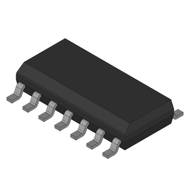
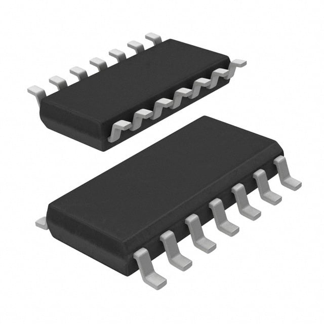
| 产品图片 |
|
| rohs | 符合RoHS无铅 / 符合限制有害物质指令(RoHS)规范要求 |
| 产品系列 | 逻辑集成电路,变换器,NXP Semiconductors HEF4069UBT,6534000B |
| 数据手册 | |
| 产品型号 | HEF4069UBT,653 |
| PCN封装 | |
| PCN组件/产地 | |
| 不同V、最大CL时的最大传播延迟 | 30ns @ 15V,50pF |
| 产品培训模块 | http://www.digikey.cn/PTM/IndividualPTM.page?site=cn&lang=zhs&ptm=24983 |
| 产品种类 | 变换器 |
| 传播延迟时间 | 90 ns, 40 ns, 25 ns |
| 低电平输出电流 | 4.2 mA |
| 供应商器件封装 | 14-SO |
| 其它名称 | 568-8083-2 |
| 包装 | 带卷 (TR) |
| 商标 | NXP Semiconductors |
| 安装类型 | 表面贴装 |
| 安装风格 | SMD/SMT |
| 封装 | Reel |
| 封装/外壳 | 14-SOIC(0.154",3.90mm 宽) |
| 封装/箱体 | SOT-108 |
| 工作温度 | -40°C ~ 125°C |
| 工厂包装数量 | 2500 |
| 最大工作温度 | + 125 C |
| 标准包装 | 2,500 |
| 特性 | - |
| 电压-电源 | 3 V ~ 15 V |
| 电流-输出高,低 | 3.4mA,3.4mA |
| 电流-静态(最大值) | 1µA |
| 电源电压-最大 | 15 V |
| 电源电压-最小 | 3 V |
| 电路数 | 6 |
| 电路数量 | 6 Circuit |
| 输入数 | 6 |
| 逻辑电平-低 | 1 V ~ 2.5 V |
| 逻辑电平-高 | 4 V ~ 12.5 V |
| 逻辑类型 | CMOS |
| 逻辑系列 | HEF4000 |
| 零件号别名 | HEF4069UBTD-T |
| 高电平输出电流 | - 4.2 mA |


- 商务部:美国ITC正式对集成电路等产品启动337调查
- 曝三星4nm工艺存在良率问题 高通将骁龙8 Gen1或转产台积电
- 太阳诱电将投资9.5亿元在常州建新厂生产MLCC 预计2023年完工
- 英特尔发布欧洲新工厂建设计划 深化IDM 2.0 战略
- 台积电先进制程称霸业界 有大客户加持明年业绩稳了
- 达到5530亿美元!SIA预计今年全球半导体销售额将创下新高
- 英特尔拟将自动驾驶子公司Mobileye上市 估值或超500亿美元
- 三星加码芯片和SET,合并消费电子和移动部门,撤换高东真等 CEO
- 三星电子宣布重大人事变动 还合并消费电子和移动部门
- 海关总署:前11个月进口集成电路产品价值2.52万亿元 增长14.8%


PDF Datasheet 数据手册内容提取
HEF4069UB Hex unbuffered inverter Rev. 9 — 16 December 2015 Product data sheet 1. General description The HEF4069UB is a general purpose hex unbuffered inverter. Each inverter has a single stage. It operates over a recommended V power supply range of 3V to 15 V referenced to V DD SS (usually ground). Unused inputs must be connected to V , V , or another input. DD SS 2. Features and benefits Fully static operation 5V, 10V, and 15V parametric ratings Standardized symmetrical output characteristics Specified from 40C to +85C and 40C to +125C Complies with JEDEC standard JESD 13-B 3. Applications Oscillator 4. Ordering information Table 1. Ordering info rmation All types operate from 40C to +125C. Type number Package Name Description Version HEF4069UBT SO14 plastic small outline package; 14leads; bodywidth3.9 mm SOT108-1 HEF4069UBTT TSSOP14 plastic thin shrink small outline package; 14leads; bodywidth4.4mm SOT402-1
HEF4069UB Nexperia Hex unbuffered inverter 5. Functional diagram (cid:20) (cid:21) (cid:20)(cid:36) (cid:20)(cid:60) (cid:22) (cid:23) (cid:21)(cid:36) (cid:21)(cid:60) (cid:24) (cid:25) (cid:22)(cid:36) (cid:22)(cid:60) (cid:28) (cid:27) (cid:23)(cid:36) (cid:23)(cid:60) (cid:57)(cid:39)(cid:39) (cid:20)(cid:20) (cid:20)(cid:19) (cid:24)(cid:36) (cid:24)(cid:60) (cid:36) (cid:60) (cid:20)(cid:22) (cid:20)(cid:21) (cid:25)(cid:36) (cid:25)(cid:60) (cid:57)(cid:54)(cid:54) (cid:19)(cid:19)(cid:20)(cid:68)(cid:68)(cid:74)(cid:20)(cid:24)(cid:21) (cid:19)(cid:19)(cid:20)(cid:68)(cid:68)(cid:74)(cid:20)(cid:24)(cid:23) Fig 1. Functional diagram Fig 2. Schematic diagram (one inverter) 6. Pinning information 6.1 Pinning (cid:20)(cid:36) (cid:20) (cid:20)(cid:23) (cid:57)(cid:39)(cid:39) (cid:20)(cid:60) (cid:21) (cid:20)(cid:22) (cid:25)(cid:36) (cid:21)(cid:36) (cid:22) (cid:20)(cid:21) (cid:25)(cid:60) (cid:21)(cid:60) (cid:23) (cid:43)(cid:40)(cid:41)(cid:23)(cid:19)(cid:25)(cid:28)(cid:56)(cid:37) (cid:20)(cid:20) (cid:24)(cid:36) (cid:22)(cid:36) (cid:24) (cid:20)(cid:19) (cid:24)(cid:60) (cid:22)(cid:60) (cid:25) (cid:28) (cid:23)(cid:36) (cid:57)(cid:54)(cid:54) (cid:26) (cid:27) (cid:23)(cid:60) (cid:19)(cid:19)(cid:20)(cid:68)(cid:68)(cid:74)(cid:20)(cid:24)(cid:22) Fig 3. Pin configuration 6.2 Pin description Table 2. Pin descripti on Symbol Pin Description 1A to 6A 1, 3, 5, 9, 11, 13 input 1Y to 6Y 2, 4, 6, 8, 10, 12 output V 7 ground (0 V) SS V 14 supply voltage DD HEF4069UB All information provided in this document is subject to legal disclaimers. © Nexperia B.V. 2017. All rights reserved Product data sheet Rev. 9 — 16 December 2015 2 of 16
HEF4069UB Nexperia Hex unbuffered inverter 7. Limiting values Table 3. Limiting valu es In accordance with the Absolute Maximum Rating System (IEC 60134). Symbol Parameter Conditions Min Max Unit V supply voltage 0.5 +18 V DD I input clamping current V <0.5V or V >V + 0.5 V - 10 mA IK I I DD V input voltage 0.5 V + 0.5 V I DD I output clamping current V <0.5V or V >V + 0.5 V - 10 mA OK O O DD I input/output current - 10 mA I/O I supply current - 50 mA DD T storage temperature 65 +150 C stg T ambient temperature 40 +125 C amb P total power dissipation T = 40 C to +125 C tot amb SO14 [1] - 500 mW TSSOP14 [2] - 500 mW P power dissipation per output - 100 mW [1] For SO14 packages: above Tamb = 70 C, Ptot derates linearly with 8mW/K. [2] For TSSOP14 packages: above Tamb = 60 C, Ptot derates linearly with 5.5mW/K. 8. Recommended operating conditions Table 4. Recommend ed operating conditions Symbol Parameter Conditions Min Typ Max Unit V supply voltage 3 - 15 V DD V input voltage 0 - V V I DD T ambient temperature in free air 40 - +125 C amb HEF4069UB All information provided in this document is subject to legal disclaimers. © Nexperia B.V. 2017. All rights reserved Product data sheet Rev. 9 — 16 December 2015 3 of 16
HEF4069UB Nexperia Hex unbuffered inverter 9. Static characteristics Table 5. Static charac teristics V = 0V; V =V or V ; unless otherwise specified. SS I SS DD Symbol Parameter Conditions V T = 40 C T = +25 C T = +85 C T = +125 C Unit DD amb amb amb amb Min Max Min Max Min Max Min Max V HIGH-level I <1A 5V 4 - 4 - 4 - 4 - V IH O input voltage 10V 8 - 8 - 8 - 8 - V 15V 12.5 - 12.5 - 12.5 - 12.5 - V V LOW-level I <1A 5V - 1 - 1 - 1 - 1 V IL O input voltage 10V - 2 - 2 - 2 - 2 V 15V - 2.5 - 2.5 - 2.5 - 2.5 V V HIGH-level I <1A 5V 4.95 - 4.95 - 4.95 - 4.95 - V OH O output voltage 10V 9.95 - 9.95 - 9.95 - 9.95 - V 15V 14.95 - 14.95 - 14.95 - 14.95 - V V LOW-level I <1A 5V - 0.05 - 0.05 - 0.05 - 0.05 V OL O output voltage 10V - 0.05 - 0.05 - 0.05 - 0.05 V 15V - 0.05 - 0.05 - 0.05 - 0.05 V I HIGH-level V = 2.5 V 5 V - 1.7 - 1.4 - 1.1 - 1.1 mA OH O output current V = 4.6 V 5 V - 0.64 - 0.5 - 0.36 - 0.36 mA O V = 9.5 V 10 V - 1.6 - 1.3 - 0.9 - 0.9 mA O V = 13.5 V 15 V - 4.2 - 3.4 - 2.4 - 2.4 mA O I LOW-level V = 0.4 V 5 V 0.64 - 0.5 - 0.36 - 0.36 - mA OL O output current V = 0.5 V 10 V 1.6 - 1.3 - 0.9 - 0.9 - mA O V = 1.5 V 15 V 4.2 - 3.4 - 2.4 - 2.4 - mA O I input leakage 15V - 0.1 - 0.1 - 1.0 - 1.0 A I current I supply current allvalid input 5V - 0.25 - 0.25 - 7.5 - 7.5 A DD combinations; 10V - 0.5 - 0.5 - 15.0 - 15.0 A I =0A O 15V - 1.0 - 1.0 - 30.0 - 30.0 A C input digital inputs - - - 7.5 - - - - pF I capacitance HEF4069UB All information provided in this document is subject to legal disclaimers. © Nexperia B.V. 2017. All rights reserved Product data sheet Rev. 9 — 16 December 2015 4 of 16
HEF4069UB Nexperia Hex unbuffered inverter 10. Dynamic characteristics Table 6. Dynamic cha racteristics T = 25 C; for waveforms see Figure4; for test circuit see Figure5. amb Symbol Parameter Conditions V Extrapolation formula[1] Min Typ Max Unit DD t HIGH to LOW nA to nY; 5V 18 ns + (0.55 ns/pF)C - 45 90 ns PHL L propagationdelay 10V 9 ns + (0.23 ns/pF)C - 20 40 ns L 15V 7 ns + (0.16 ns/pF)C - 15 25 ns L t LOW to HIGH nA to nY 5V 13 ns + (0.55 ns/pF)C - 40 80 ns PLH L propagationdelay 10V 9 ns + (0.23 ns/pF)C - 20 40 ns L 15V 7 ns + (0.16 ns/pF)C - 15 30 ns L t HIGH to LOW output output nY 5V 10 ns + (1.00 ns/pF)C - 60 120 ns THL L transitiontime 10V 9 ns + (0.42 ns/pF)C - 30 60 ns L 15V 6 ns + (0.28 ns/pF)C - 20 40 ns L t LOW to HIGH output output nY 5V 10 ns + (1.00 ns/pF)C - 60 120 ns TLH L transitiontime 10V 9 ns + (0.42 ns/pF)C - 30 60 ns L 15V 6 ns + (0.28 ns/pF)C - 20 40 ns L [1] The typical value of the propagation delay and output transition time can be calculated with the extrapolation formula (C in pF). L Table 7. Dynamic po wer dissipation V = 0V; t = t 20ns; T = 25 C. SS r f amb Symbol Parameter V Typical formula Where DD P dynamic power dissipation 5V P = 600 f + (f C ) V 2 (W) f = input frequency in MHz; D D i o L DD i 10V PD = 4000 fi + (fo CL) VDD2 (W) fo = output frequency in MHz; 15V PD = 22000 fi + (fo CL) VDD2 (W) CL = output load capacitance in pF; (f C ) = sum of the outputs; o L V = supply voltage in V. DD HEF4069UB All information provided in this document is subject to legal disclaimers. © Nexperia B.V. 2017. All rights reserved Product data sheet Rev. 9 — 16 December 2015 5 of 16
HEF4069UB Nexperia Hex unbuffered inverter 11. Waveforms (cid:87)(cid:85)(cid:3) (cid:87)(cid:73) (cid:57)(cid:44) (cid:28)(cid:19)(cid:3)(cid:8) (cid:76)(cid:81)(cid:83)(cid:88)(cid:87) (cid:57)(cid:48) (cid:20)(cid:19)(cid:3)(cid:8) (cid:19)(cid:3)(cid:57) (cid:87)(cid:51)(cid:43)(cid:47) (cid:87)(cid:51)(cid:47)(cid:43) (cid:57)(cid:50)(cid:43) (cid:28)(cid:19)(cid:3)(cid:8) (cid:82)(cid:88)(cid:87)(cid:83)(cid:88)(cid:87) (cid:57)(cid:48) (cid:20)(cid:19)(cid:3)(cid:8) (cid:57)(cid:50)(cid:47) (cid:87)(cid:55)(cid:43)(cid:47)(cid:3) (cid:87)(cid:55)(cid:47)(cid:43)(cid:3) (cid:19)(cid:19)(cid:20)(cid:68)(cid:68)(cid:74)(cid:20)(cid:27)(cid:24) Measurement points: V = 0.5V . M DD Logic levels: V and V are typical output voltage levels that occur with the output load. OL OH Fig 4. Propagation delay and transition times (cid:57)(cid:39)(cid:39) (cid:57)(cid:44) (cid:57)(cid:50) (cid:42) (cid:39)(cid:56)(cid:55) (cid:53)(cid:55) (cid:38)(cid:47) (cid:19)(cid:19)(cid:20)(cid:68)(cid:68)(cid:74)(cid:20)(cid:27)(cid:21) Definitions for test circuit: CL=load capacitance including jig and probe capacitance; RT=termination resistance should be equal to the output impedance Zo of the pulse generator; For test data refer to Table8. Fig 5. Test circuit for measuring switching times Table 8. Test data Supply voltage Input Load V V t, t C DD I r f L 5V to 15V V or V 20ns 50 pF SS DD HEF4069UB All information provided in this document is subject to legal disclaimers. © Nexperia B.V. 2017. All rights reserved Product data sheet Rev. 9 — 16 December 2015 6 of 16
HEF4069UB Nexperia Hex unbuffered inverter 11.1 Transfer characteristics (cid:19)(cid:19)(cid:20)(cid:68)(cid:68)(cid:74)(cid:20)(cid:24)(cid:28) (cid:19)(cid:19)(cid:20)(cid:68)(cid:68)(cid:74)(cid:20)(cid:25)(cid:19) (cid:24)(cid:17)(cid:19) (cid:24)(cid:19)(cid:19) (cid:20)(cid:19) (cid:20)(cid:19) (cid:57)(cid:50)(cid:3) (cid:44)(cid:39)(cid:3) (cid:57)(cid:50)(cid:3) (cid:44)(cid:39)(cid:3) (cid:11)(cid:57)(cid:12) (cid:11)(cid:151)(cid:36)(cid:12) (cid:11)(cid:57)(cid:12) (cid:11)(cid:80)(cid:36)(cid:12) (cid:21)(cid:17)(cid:24)(cid:3) (cid:21)(cid:24)(cid:19) (cid:24) (cid:24) (cid:3) (cid:11)(cid:21)(cid:12) (cid:11)(cid:20)(cid:12) (cid:11)(cid:21)(cid:12) (cid:11)(cid:21)(cid:12)(cid:3) (cid:11)(cid:20)(cid:12)(cid:3) (cid:11)(cid:21)(cid:12)(cid:3) (cid:19) (cid:19) (cid:19) (cid:19) (cid:19) (cid:21)(cid:17)(cid:24) (cid:24)(cid:17)(cid:19) (cid:19) (cid:24) (cid:20)(cid:19) (cid:57)(cid:44)(cid:3)(cid:11)(cid:57)(cid:12) (cid:57)(cid:44)(cid:3)(cid:11)(cid:57)(cid:12) a. V = 5V; I = 0A b. V = 10V; I = 0A DD O DD O (cid:19)(cid:19)(cid:20)(cid:68)(cid:68)(cid:74)(cid:20)(cid:25)(cid:20) (cid:21)(cid:19) (cid:21)(cid:19) (cid:57)(cid:50)(cid:3) (cid:44)(cid:39)(cid:3) (cid:11)(cid:57)(cid:12) (cid:11)(cid:80)(cid:36)(cid:12) (cid:20)(cid:19)(cid:3) (cid:20)(cid:19) (cid:3) (cid:11)(cid:21)(cid:12)(cid:3) (cid:11)(cid:20)(cid:12)(cid:3) (cid:11)(cid:21)(cid:12)(cid:3) (cid:19) (cid:19) (cid:19) (cid:20)(cid:19) (cid:21)(cid:19) (cid:57)(cid:44)(cid:3)(cid:11)(cid:57)(cid:12) c. V = 15V; I = 0A DD O (1) V = output voltage. O (2) I = drain current. D Fig 6. Typical transfer characteristics HEF4069UB All information provided in this document is subject to legal disclaimers. © Nexperia B.V. 2017. All rights reserved Product data sheet Rev. 9 — 16 December 2015 7 of 16
HEF4069UB Nexperia Hex unbuffered inverter 12. Application information Some examples of applications for the HEF4069UB. Figure7 shows an astable relaxation oscillator using two HEF4069UB inverters and 2 BAW62 diodes. The oscillation frequency is mainly determined by R1 C1, provided R1<<R2 and R2C2<<R1C1. The function of R2 is to minimize the influence of the forward voltage across the protection diodes on the frequency; C2 is a stray (parasitic) capacitance. The period T is given by T =T +T , p p 1 2 where: V +V T = R1C1In----D----D--------------S--T-- 1 V ST 2V –V T = R1C1In --------D---D--------------S--T-- 2 V –V DD ST V = the signal threshold level of the inverter. ST The period is fairly independent of V , V and temperature. The duty factor, however, is DD ST influenced by V . ST (cid:57)(cid:39)(cid:39) (cid:57)(cid:39)(cid:39) (cid:36) (cid:20)(cid:18)(cid:25)(cid:3)(cid:43)(cid:40)(cid:41)(cid:23)(cid:19)(cid:25)(cid:28)(cid:56)(cid:37) (cid:20)(cid:18)(cid:25)(cid:3)(cid:43)(cid:40)(cid:41)(cid:23)(cid:19)(cid:25)(cid:28)(cid:56)(cid:37) (cid:19)(cid:3)(cid:57) (cid:39) (cid:36) (cid:37) (cid:57)(cid:39)(cid:39) (cid:38)(cid:21) (cid:53)(cid:21) (cid:53)(cid:20) (cid:38)(cid:20) (cid:37) (cid:57)(cid:54)(cid:54) (cid:19)(cid:3)(cid:57) (cid:38) (cid:20)(cid:17)(cid:24)(cid:57)(cid:39)(cid:39) (cid:57)(cid:39)(cid:39) (cid:38) (cid:19)(cid:17)(cid:24)(cid:57)(cid:39)(cid:39) (cid:19)(cid:3)(cid:57) (cid:16)(cid:19)(cid:17)(cid:24)(cid:57)(cid:39)(cid:39) (cid:57)(cid:39)(cid:39) (cid:39) (cid:19)(cid:17)(cid:24)(cid:57)(cid:39)(cid:39) (cid:19)(cid:3)(cid:57) (cid:73)(cid:82)(cid:85)(cid:90)(cid:68)(cid:85)(cid:71)(cid:3)(cid:89)(cid:82)(cid:79)(cid:87)(cid:68)(cid:74)(cid:72)(cid:3) (cid:70)(cid:79)(cid:68)(cid:80)(cid:83)(cid:76)(cid:81)(cid:74)(cid:3)(cid:71)(cid:76)(cid:82)(cid:71)(cid:72) (cid:19)(cid:19)(cid:20)(cid:68)(cid:68)(cid:74)(cid:20)(cid:25)(cid:21) Fig 7. Astable relaxation oscillator HEF4069UB All information provided in this document is subject to legal disclaimers. © Nexperia B.V. 2017. All rights reserved Product data sheet Rev. 9 — 16 December 2015 8 of 16
HEF4069UB Nexperia Hex unbuffered inverter Figure8 shows a crystal oscillator for frequencies up to 10 MHz using two HEF4069UB inverters. The second inverter amplifies the oscillator output voltage to a level sufficient to drive other Local Oxidation CMOS (LOCMOS) circuits. (cid:20)(cid:3)(cid:48)(cid:525) (cid:21)(cid:21)(cid:3)(cid:83)(cid:41) (cid:20)(cid:3)(cid:48)(cid:525) (cid:21)(cid:3)(cid:48)(cid:43)(cid:93) (cid:21)(cid:17)(cid:21)(cid:3)(cid:78)(cid:525) (cid:20)(cid:19)(cid:19)(cid:3)(cid:83)(cid:41) (cid:21)(cid:21)(cid:3)(cid:83)(cid:41) (cid:20)(cid:18)(cid:25)(cid:3)(cid:43)(cid:40)(cid:41)(cid:23)(cid:19)(cid:25)(cid:28)(cid:56)(cid:37) (cid:20)(cid:18)(cid:25)(cid:3)(cid:43)(cid:40)(cid:41)(cid:23)(cid:19)(cid:25)(cid:28)(cid:56)(cid:37) (cid:19)(cid:19)(cid:20)(cid:68)(cid:68)(cid:74)(cid:20)(cid:24)(cid:24) The output inverter is used to amplify the oscillator output voltage to a level sufficient to drive other LOCMOS circuits. Fig 8. Crystal oscillator Figure9 and Figure10 show voltage gain and supply current. Figure11 shows the test set-up and an example of an analog amplifier using one HEF4069UB. (cid:19)(cid:19)(cid:20)(cid:68)(cid:68)(cid:74)(cid:20)(cid:24)(cid:25) (cid:19)(cid:19)(cid:20)(cid:68)(cid:68)(cid:74)(cid:20)(cid:24)(cid:26) (cid:26)(cid:24) (cid:21)(cid:19) (cid:44)(cid:39)(cid:39)(cid:3) (cid:74)(cid:68)(cid:76)(cid:81)(cid:3) (cid:11)(cid:80)(cid:36)(cid:12) (cid:11)(cid:57)(cid:50)(cid:18)(cid:57)(cid:44)(cid:12) (cid:20)(cid:24) (cid:24)(cid:19) (cid:87)(cid:92)(cid:83) (cid:87)(cid:92)(cid:83) (cid:20)(cid:19) (cid:21)(cid:24) (cid:24) (cid:19) (cid:19) (cid:19) (cid:24) (cid:20)(cid:19) (cid:20)(cid:24) (cid:19) (cid:24) (cid:20)(cid:19) (cid:20)(cid:24) (cid:57)(cid:39)(cid:39)(cid:3)(cid:11)(cid:57)(cid:12) (cid:57)(cid:39)(cid:39)(cid:3)(cid:11)(cid:57)(cid:12) Fig 9. Typical voltage gain as a function of Fig 10. Typical supply current as a function of supplyvoltage supplyvoltage (cid:22)(cid:22)(cid:19)(cid:3)(cid:78)(cid:525) (cid:20)(cid:18)(cid:25)(cid:3)(cid:43)(cid:40)(cid:41)(cid:23)(cid:19)(cid:25)(cid:28)(cid:56)(cid:37) (cid:19)(cid:19)(cid:20)(cid:68)(cid:68)(cid:74)(cid:20)(cid:24)(cid:27) Fig 11. Test set-up HEF4069UB All information provided in this document is subject to legal disclaimers. © Nexperia B.V. 2017. All rights reserved Product data sheet Rev. 9 — 16 December 2015 9 of 16
HEF4069UB Nexperia Hex unbuffered inverter Figure12 shows typical forward transconductance and Figure13 shows the test set-up. (cid:19)(cid:19)(cid:20)(cid:68)(cid:68)(cid:74)(cid:20)(cid:25)(cid:23) (cid:20)(cid:19) (cid:74)(cid:73)(cid:86)(cid:3) (cid:11)(cid:80)(cid:36)(cid:18)(cid:57)(cid:12) (cid:11)(cid:20)(cid:12) (cid:26)(cid:17)(cid:24) (cid:11)(cid:21)(cid:12) (cid:53)(cid:69)(cid:76)(cid:68)(cid:86)(cid:3)(cid:32)(cid:3)(cid:24)(cid:25)(cid:19)(cid:3)(cid:78)(cid:525) (cid:24)(cid:17)(cid:19) (cid:11)(cid:22)(cid:12) (cid:57)(cid:39)(cid:39) (cid:21)(cid:17)(cid:24) (cid:19)(cid:17)(cid:23)(cid:26)(cid:3)(cid:151)(cid:41) (cid:76)(cid:81)(cid:83)(cid:88)(cid:87) (cid:82)(cid:88)(cid:87)(cid:83)(cid:88)(cid:87) (cid:20)(cid:19)(cid:19)(cid:3)(cid:151)(cid:41) (cid:57)(cid:76) (cid:36) (cid:44)(cid:82) (cid:19) (cid:19) (cid:24) (cid:20)(cid:19) (cid:20)(cid:24) (cid:57)(cid:54)(cid:54) (cid:57)(cid:39)(cid:39)(cid:3)(cid:11)(cid:57)(cid:12) (cid:19)(cid:19)(cid:20)(cid:68)(cid:68)(cid:74)(cid:20)(cid:25)(cid:22) (1) Average +2; where: ‘’ is the standard deviation. dI (2) Average. gfs= d----V--o-- at VO is constant. i (3) Average 2; where: ‘’ is the standard deviation. f.= 1kHz i Fig 12. Typical forward transconductanceas a Fig 13. Test set-up function of supply voltage at T = 25C amb HEF4069UB All information provided in this document is subject to legal disclaimers. © Nexperia B.V. 2017. All rights reserved Product data sheet Rev. 9 — 16 December 2015 10 of 16
HEF4069UB Nexperia Hex unbuffered inverter 13. Package outline (cid:54)(cid:50)(cid:20)(cid:23)(cid:29)(cid:3)(cid:83)(cid:79)(cid:68)(cid:86)(cid:87)(cid:76)(cid:70)(cid:3)(cid:86)(cid:80)(cid:68)(cid:79)(cid:79)(cid:3)(cid:82)(cid:88)(cid:87)(cid:79)(cid:76)(cid:81)(cid:72)(cid:3)(cid:83)(cid:68)(cid:70)(cid:78)(cid:68)(cid:74)(cid:72)(cid:30)(cid:3)(cid:20)(cid:23)(cid:3)(cid:79)(cid:72)(cid:68)(cid:71)(cid:86)(cid:30)(cid:3)(cid:69)(cid:82)(cid:71)(cid:92)(cid:3)(cid:90)(cid:76)(cid:71)(cid:87)(cid:75)(cid:3)(cid:22)(cid:17)(cid:28)(cid:3)(cid:80)(cid:80)(cid:3) (cid:54)(cid:50)(cid:55)(cid:20)(cid:19)(cid:27)(cid:16)(cid:20)(cid:3) (cid:39)(cid:3) (cid:40)(cid:3) (cid:36)(cid:3) (cid:59)(cid:3) (cid:70)(cid:3) (cid:92)(cid:3) (cid:43)(cid:3)(cid:40)(cid:3) (cid:89)(cid:3)(cid:48)(cid:3) (cid:36)(cid:3) (cid:61)(cid:3) (cid:20)(cid:23)(cid:3) (cid:27)(cid:3) (cid:52)(cid:3) (cid:36)(cid:3)(cid:21)(cid:3)(cid:36)(cid:3)(cid:20)(cid:3) (cid:11)(cid:36)(cid:3)(cid:22)(cid:3)(cid:3)(cid:12)(cid:3) (cid:36)(cid:3) (cid:83)(cid:76)(cid:81)(cid:3)(cid:20)(cid:3)(cid:76)(cid:81)(cid:71)(cid:72)(cid:91)(cid:3) (cid:537)(cid:3) (cid:47)(cid:3)(cid:83)(cid:3) (cid:20)(cid:3) (cid:26)(cid:3) (cid:47)(cid:3) (cid:72)(cid:3) (cid:90)(cid:3)(cid:48)(cid:3) (cid:71)(cid:72)(cid:87)(cid:68)(cid:76)(cid:79)(cid:3)(cid:59)(cid:3) (cid:69)(cid:3)(cid:83)(cid:3) (cid:19)(cid:3) (cid:21)(cid:17)(cid:24)(cid:3) (cid:24)(cid:3)(cid:80)(cid:80)(cid:3) (cid:86)(cid:70)(cid:68)(cid:79)(cid:72)(cid:3) (cid:39)(cid:44)(cid:48)(cid:40)(cid:49)(cid:54)(cid:44)(cid:50)(cid:49)(cid:54)(cid:3)(cid:11)(cid:76)(cid:81)(cid:70)(cid:75)(cid:3)(cid:71)(cid:76)(cid:80)(cid:72)(cid:81)(cid:86)(cid:76)(cid:82)(cid:81)(cid:86)(cid:3)(cid:68)(cid:85)(cid:72)(cid:3)(cid:71)(cid:72)(cid:85)(cid:76)(cid:89)(cid:72)(cid:71)(cid:3)(cid:73)(cid:85)(cid:82)(cid:80)(cid:3)(cid:87)(cid:75)(cid:72)(cid:3)(cid:82)(cid:85)(cid:76)(cid:74)(cid:76)(cid:81)(cid:68)(cid:79)(cid:3)(cid:80)(cid:80)(cid:3)(cid:71)(cid:76)(cid:80)(cid:72)(cid:81)(cid:86)(cid:76)(cid:82)(cid:81)(cid:86)(cid:12)(cid:3) (cid:56)(cid:49)(cid:44)(cid:55)(cid:3) (cid:80)(cid:36)(cid:68)(cid:91)(cid:3)(cid:17)(cid:3) (cid:36)(cid:3)(cid:20)(cid:3) (cid:36)(cid:3)(cid:21)(cid:3) (cid:36)(cid:3)(cid:22)(cid:3) (cid:69)(cid:3)(cid:83)(cid:3) (cid:70)(cid:3) (cid:39)(cid:3)(cid:11)(cid:20)(cid:12)(cid:3) (cid:40)(cid:3)(cid:11)(cid:20)(cid:12)(cid:3) (cid:72)(cid:3) (cid:43)(cid:3)(cid:40)(cid:3) (cid:47)(cid:3) (cid:47)(cid:3)(cid:83)(cid:3) (cid:52)(cid:3) (cid:89)(cid:3) (cid:90)(cid:3) (cid:92)(cid:3) (cid:61)(cid:3)(cid:11)(cid:20)(cid:12)(cid:3) (cid:537)(cid:3) (cid:80)(cid:80)(cid:3) (cid:20)(cid:17)(cid:26)(cid:24)(cid:3) (cid:19)(cid:17)(cid:21)(cid:24)(cid:3) (cid:20)(cid:17)(cid:23)(cid:24)(cid:3) (cid:19)(cid:17)(cid:21)(cid:24)(cid:3) (cid:19)(cid:17)(cid:23)(cid:28)(cid:3) (cid:19)(cid:17)(cid:21)(cid:24)(cid:3) (cid:27)(cid:17)(cid:26)(cid:24)(cid:3) (cid:23)(cid:17)(cid:19)(cid:3) (cid:20)(cid:17)(cid:21)(cid:26)(cid:3) (cid:25)(cid:17)(cid:21)(cid:3) (cid:20)(cid:17)(cid:19)(cid:3)(cid:24)(cid:3) (cid:20)(cid:17)(cid:19)(cid:3) (cid:19)(cid:17)(cid:26)(cid:3) (cid:19)(cid:17)(cid:21)(cid:24)(cid:3) (cid:19)(cid:17)(cid:21)(cid:24)(cid:3) (cid:19)(cid:17)(cid:20)(cid:3) (cid:19)(cid:17)(cid:26)(cid:3) (cid:19)(cid:17)(cid:20)(cid:19)(cid:3) (cid:20)(cid:17)(cid:21)(cid:24)(cid:3) (cid:19)(cid:17)(cid:22)(cid:25)(cid:3) (cid:19)(cid:17)(cid:20)(cid:28)(cid:3) (cid:27)(cid:17)(cid:24)(cid:24)(cid:3) (cid:22)(cid:17)(cid:27)(cid:3) (cid:24)(cid:17)(cid:27)(cid:3) (cid:19)(cid:17)(cid:23)(cid:3) (cid:19)(cid:17)(cid:25)(cid:3) (cid:19)(cid:17)(cid:22)(cid:3) (cid:27)(cid:3)(cid:82)(cid:3) (cid:19)(cid:17)(cid:19)(cid:20)(cid:19)(cid:3) (cid:19)(cid:17)(cid:19)(cid:24)(cid:26)(cid:3) (cid:19)(cid:17)(cid:19)(cid:20)(cid:28)(cid:3)(cid:19)(cid:17)(cid:19)(cid:20)(cid:19)(cid:19)(cid:3) (cid:19)(cid:17)(cid:22)(cid:24)(cid:3) (cid:19)(cid:17)(cid:20)(cid:25)(cid:3) (cid:19)(cid:17)(cid:21)(cid:23)(cid:23)(cid:3) (cid:19)(cid:17)(cid:19)(cid:22)(cid:28)(cid:3) (cid:19)(cid:17)(cid:19)(cid:21)(cid:27)(cid:3) (cid:19)(cid:17)(cid:19)(cid:21)(cid:27)(cid:3) (cid:19)(cid:3)(cid:82)(cid:3) (cid:76)(cid:81)(cid:70)(cid:75)(cid:72)(cid:86)(cid:3) (cid:19)(cid:17)(cid:19)(cid:25)(cid:28)(cid:3) (cid:19)(cid:17)(cid:19)(cid:20)(cid:3) (cid:19)(cid:17)(cid:19)(cid:24)(cid:3) (cid:19)(cid:17)(cid:19)(cid:23)(cid:20)(cid:3) (cid:19)(cid:17)(cid:19)(cid:20)(cid:3) (cid:19)(cid:17)(cid:19)(cid:20)(cid:3) (cid:19)(cid:17)(cid:19)(cid:19)(cid:23)(cid:3) (cid:19)(cid:17)(cid:19)(cid:19)(cid:23)(cid:3) (cid:19)(cid:17)(cid:19)(cid:23)(cid:28)(cid:3) (cid:19)(cid:17)(cid:19)(cid:20)(cid:23)(cid:3)(cid:19)(cid:17)(cid:19)(cid:19)(cid:26)(cid:24)(cid:3) (cid:19)(cid:17)(cid:22)(cid:23)(cid:3) (cid:19)(cid:17)(cid:20)(cid:24)(cid:3) (cid:19)(cid:17)(cid:21)(cid:21)(cid:27)(cid:3) (cid:19)(cid:17)(cid:19)(cid:20)(cid:25)(cid:3) (cid:19)(cid:17)(cid:19)(cid:21)(cid:23)(cid:3) (cid:19)(cid:17)(cid:19)(cid:20)(cid:21)(cid:3) (cid:49)(cid:82)(cid:87)(cid:72)(cid:3) (cid:20)(cid:17)(cid:3)(cid:51)(cid:79)(cid:68)(cid:86)(cid:87)(cid:76)(cid:70)(cid:3)(cid:82)(cid:85)(cid:3)(cid:80)(cid:72)(cid:87)(cid:68)(cid:79)(cid:3)(cid:83)(cid:85)(cid:82)(cid:87)(cid:85)(cid:88)(cid:86)(cid:76)(cid:82)(cid:81)(cid:86)(cid:3)(cid:82)(cid:73)(cid:3)(cid:19)(cid:17)(cid:20)(cid:24)(cid:3)(cid:80)(cid:80)(cid:3)(cid:11)(cid:19)(cid:17)(cid:19)(cid:19)(cid:25)(cid:3)(cid:76)(cid:81)(cid:70)(cid:75)(cid:12)(cid:3)(cid:80)(cid:68)(cid:91)(cid:76)(cid:80)(cid:88)(cid:80)(cid:3)(cid:83)(cid:72)(cid:85)(cid:3)(cid:86)(cid:76)(cid:71)(cid:72)(cid:3)(cid:68)(cid:85)(cid:72)(cid:3)(cid:81)(cid:82)(cid:87)(cid:3)(cid:76)(cid:81)(cid:70)(cid:79)(cid:88)(cid:71)(cid:72)(cid:71)(cid:17)(cid:3)(cid:3) (cid:50)(cid:56)(cid:55)(cid:47)(cid:44)(cid:49)(cid:40)(cid:3) (cid:3)(cid:53)(cid:40)(cid:41)(cid:40)(cid:53)(cid:40)(cid:49)(cid:38)(cid:40)(cid:54)(cid:3) (cid:40)(cid:56)(cid:53)(cid:50)(cid:51)(cid:40)(cid:36)(cid:49)(cid:3) (cid:44)(cid:54)(cid:54)(cid:56)(cid:40)(cid:3)(cid:39)(cid:36)(cid:55)(cid:40)(cid:3) (cid:57)(cid:40)(cid:53)(cid:54)(cid:44)(cid:50)(cid:49)(cid:3) (cid:3)(cid:44)(cid:40)(cid:38)(cid:3) (cid:3)(cid:45)(cid:40)(cid:39)(cid:40)(cid:38)(cid:3) (cid:3)(cid:45)(cid:40)(cid:44)(cid:55)(cid:36)(cid:3) (cid:51)(cid:53)(cid:50)(cid:45)(cid:40)(cid:38)(cid:55)(cid:44)(cid:50)(cid:49)(cid:3) (cid:28)(cid:28)(cid:16)(cid:20)(cid:21)(cid:16)(cid:21)(cid:26)(cid:3) (cid:3)(cid:54)(cid:50)(cid:55)(cid:20)(cid:19)(cid:27)(cid:16)(cid:20)(cid:3) (cid:3)(cid:19)(cid:26)(cid:25)(cid:40)(cid:19)(cid:25)(cid:3) (cid:3)(cid:48)(cid:54)(cid:16)(cid:19)(cid:20)(cid:21)(cid:3) (cid:19)(cid:22)(cid:16)(cid:19)(cid:21)(cid:16)(cid:20)(cid:28)(cid:3) Fig 14. Package outline SOT108-1 (SO14) HEF4069UB All information provided in this document is subject to legal disclaimers. © Nexperia B.V. 2017. All rights reserved Product data sheet Rev. 9 — 16 December 2015 11 of 16
HEF4069UB Nexperia Hex unbuffered inverter (cid:55)(cid:54)(cid:54)(cid:50)(cid:51)(cid:20)(cid:23)(cid:29)(cid:3)(cid:83)(cid:79)(cid:68)(cid:86)(cid:87)(cid:76)(cid:70)(cid:3)(cid:87)(cid:75)(cid:76)(cid:81)(cid:3)(cid:86)(cid:75)(cid:85)(cid:76)(cid:81)(cid:78)(cid:3)(cid:86)(cid:80)(cid:68)(cid:79)(cid:79)(cid:3)(cid:82)(cid:88)(cid:87)(cid:79)(cid:76)(cid:81)(cid:72)(cid:3)(cid:83)(cid:68)(cid:70)(cid:78)(cid:68)(cid:74)(cid:72)(cid:30)(cid:3)(cid:20)(cid:23)(cid:3)(cid:79)(cid:72)(cid:68)(cid:71)(cid:86)(cid:30)(cid:3)(cid:69)(cid:82)(cid:71)(cid:92)(cid:3)(cid:90)(cid:76)(cid:71)(cid:87)(cid:75)(cid:3)(cid:23)(cid:17)(cid:23)(cid:3)(cid:80)(cid:80)(cid:3) (cid:54)(cid:50)(cid:55)(cid:23)(cid:19)(cid:21)(cid:16)(cid:20)(cid:3) (cid:39)(cid:3) (cid:40)(cid:3) (cid:36)(cid:3) (cid:59)(cid:3) (cid:70)(cid:3) (cid:92)(cid:3) (cid:43)(cid:3)(cid:40)(cid:3) (cid:89)(cid:3)(cid:48)(cid:3) (cid:36)(cid:3) (cid:61)(cid:3) (cid:20)(cid:23)(cid:3) (cid:27)(cid:3) (cid:52)(cid:3) (cid:36)(cid:3)(cid:21)(cid:3) (cid:11)(cid:36)(cid:3)(cid:22)(cid:3)(cid:3)(cid:12)(cid:3) (cid:36)(cid:3) (cid:83)(cid:76)(cid:81)(cid:3)(cid:20)(cid:3)(cid:76)(cid:81)(cid:71)(cid:72)(cid:91)(cid:3) (cid:36)(cid:3)(cid:20)(cid:3) (cid:537)(cid:3) (cid:47)(cid:3)(cid:83)(cid:3) (cid:47)(cid:3) (cid:20)(cid:3) (cid:26)(cid:3) (cid:71)(cid:72)(cid:87)(cid:68)(cid:76)(cid:79)(cid:3)(cid:59)(cid:3) (cid:90)(cid:3)(cid:48)(cid:3) (cid:72)(cid:3) (cid:69)(cid:3)(cid:83)(cid:3) (cid:19)(cid:3) (cid:21)(cid:17)(cid:24)(cid:3) (cid:24)(cid:3)(cid:80)(cid:80)(cid:3) (cid:86)(cid:70)(cid:68)(cid:79)(cid:72)(cid:3) (cid:39)(cid:44)(cid:48)(cid:40)(cid:49)(cid:54)(cid:44)(cid:50)(cid:49)(cid:54)(cid:3)(cid:11)(cid:80)(cid:80)(cid:3)(cid:68)(cid:85)(cid:72)(cid:3)(cid:87)(cid:75)(cid:72)(cid:3)(cid:82)(cid:85)(cid:76)(cid:74)(cid:76)(cid:81)(cid:68)(cid:79)(cid:3)(cid:71)(cid:76)(cid:80)(cid:72)(cid:81)(cid:86)(cid:76)(cid:82)(cid:81)(cid:86)(cid:12)(cid:3) (cid:56)(cid:49)(cid:44)(cid:55)(cid:3) (cid:80)(cid:36)(cid:68)(cid:91)(cid:3)(cid:17)(cid:3) (cid:36)(cid:3)(cid:20)(cid:3) (cid:36)(cid:3)(cid:21)(cid:3) (cid:36)(cid:3)(cid:22)(cid:3) (cid:69)(cid:3)(cid:83)(cid:3) (cid:70)(cid:3) (cid:39)(cid:3)(cid:11)(cid:20)(cid:12)(cid:3) (cid:40)(cid:3)(cid:11)(cid:21)(cid:12)(cid:3) (cid:72)(cid:3) (cid:43)(cid:3)(cid:40)(cid:3) (cid:47)(cid:3) (cid:47)(cid:3)(cid:83)(cid:3) (cid:52)(cid:3) (cid:89)(cid:3) (cid:90)(cid:3) (cid:92)(cid:3) (cid:61)(cid:3)(cid:11)(cid:20)(cid:12)(cid:3) (cid:537)(cid:3) (cid:19)(cid:17)(cid:20)(cid:24)(cid:3) (cid:19)(cid:17)(cid:28)(cid:24)(cid:3) (cid:19)(cid:17)(cid:22)(cid:19)(cid:3) (cid:19)(cid:17)(cid:21)(cid:3) (cid:24)(cid:17)(cid:20)(cid:3) (cid:23)(cid:17)(cid:24)(cid:3) (cid:25)(cid:17)(cid:25)(cid:3) (cid:19)(cid:17)(cid:26)(cid:24)(cid:3) (cid:19)(cid:17)(cid:23)(cid:3) (cid:19)(cid:17)(cid:26)(cid:21)(cid:3) (cid:27)(cid:3)(cid:82)(cid:3) (cid:80)(cid:80)(cid:3) (cid:20)(cid:17)(cid:20)(cid:3) (cid:19)(cid:17)(cid:19)(cid:24)(cid:3) (cid:19)(cid:17)(cid:27)(cid:19)(cid:3) (cid:19)(cid:17)(cid:21)(cid:24)(cid:3) (cid:19)(cid:17)(cid:20)(cid:28)(cid:3) (cid:19)(cid:17)(cid:20)(cid:3) (cid:23)(cid:17)(cid:28)(cid:3) (cid:23)(cid:17)(cid:22)(cid:3) (cid:19)(cid:17)(cid:25)(cid:24)(cid:3) (cid:25)(cid:17)(cid:21)(cid:3) (cid:20)(cid:3) (cid:19)(cid:17)(cid:24)(cid:19)(cid:3) (cid:19)(cid:17)(cid:22)(cid:3) (cid:19)(cid:17)(cid:21)(cid:3) (cid:19)(cid:17)(cid:20)(cid:22)(cid:3) (cid:19)(cid:17)(cid:20)(cid:3) (cid:19)(cid:17)(cid:22)(cid:27)(cid:3) (cid:19)(cid:3)(cid:82)(cid:3) (cid:49)(cid:82)(cid:87)(cid:72)(cid:86)(cid:3) (cid:20)(cid:17)(cid:3)(cid:51)(cid:79)(cid:68)(cid:86)(cid:87)(cid:76)(cid:70)(cid:3)(cid:82)(cid:85)(cid:3)(cid:80)(cid:72)(cid:87)(cid:68)(cid:79)(cid:3)(cid:83)(cid:85)(cid:82)(cid:87)(cid:85)(cid:88)(cid:86)(cid:76)(cid:82)(cid:81)(cid:86)(cid:3)(cid:82)(cid:73)(cid:3)(cid:19)(cid:17)(cid:20)(cid:24)(cid:3)(cid:80)(cid:80)(cid:3)(cid:80)(cid:68)(cid:91)(cid:76)(cid:80)(cid:88)(cid:80)(cid:3)(cid:83)(cid:72)(cid:85)(cid:3)(cid:86)(cid:76)(cid:71)(cid:72)(cid:3)(cid:68)(cid:85)(cid:72)(cid:3)(cid:81)(cid:82)(cid:87)(cid:3)(cid:76)(cid:81)(cid:70)(cid:79)(cid:88)(cid:71)(cid:72)(cid:71)(cid:17)(cid:3) (cid:21)(cid:17)(cid:3)(cid:51)(cid:79)(cid:68)(cid:86)(cid:87)(cid:76)(cid:70)(cid:3)(cid:76)(cid:81)(cid:87)(cid:72)(cid:85)(cid:79)(cid:72)(cid:68)(cid:71)(cid:3)(cid:83)(cid:85)(cid:82)(cid:87)(cid:85)(cid:88)(cid:86)(cid:76)(cid:82)(cid:81)(cid:86)(cid:3)(cid:82)(cid:73)(cid:3)(cid:19)(cid:17)(cid:21)(cid:24)(cid:3)(cid:80)(cid:80)(cid:3)(cid:80)(cid:68)(cid:91)(cid:76)(cid:80)(cid:88)(cid:80)(cid:3)(cid:83)(cid:72)(cid:85)(cid:3)(cid:86)(cid:76)(cid:71)(cid:72)(cid:3)(cid:68)(cid:85)(cid:72)(cid:3)(cid:81)(cid:82)(cid:87)(cid:3)(cid:76)(cid:81)(cid:70)(cid:79)(cid:88)(cid:71)(cid:72)(cid:71)(cid:17)(cid:3) (cid:50)(cid:56)(cid:55)(cid:47)(cid:44)(cid:49)(cid:40)(cid:3) (cid:3)(cid:53)(cid:40)(cid:41)(cid:40)(cid:53)(cid:40)(cid:49)(cid:38)(cid:40)(cid:54)(cid:3) (cid:40)(cid:56)(cid:53)(cid:50)(cid:51)(cid:40)(cid:36)(cid:49)(cid:3) (cid:44)(cid:54)(cid:54)(cid:56)(cid:40)(cid:3)(cid:39)(cid:36)(cid:55)(cid:40)(cid:3) (cid:57)(cid:40)(cid:53)(cid:54)(cid:44)(cid:50)(cid:49)(cid:3) (cid:3)(cid:44)(cid:40)(cid:38)(cid:3) (cid:3)(cid:45)(cid:40)(cid:39)(cid:40)(cid:38)(cid:3) (cid:3)(cid:45)(cid:40)(cid:44)(cid:55)(cid:36)(cid:3) (cid:51)(cid:53)(cid:50)(cid:45)(cid:40)(cid:38)(cid:55)(cid:44)(cid:50)(cid:49)(cid:3) (cid:28)(cid:28)(cid:16)(cid:20)(cid:21)(cid:16)(cid:21)(cid:26)(cid:3) (cid:3)(cid:54)(cid:50)(cid:55)(cid:23)(cid:19)(cid:21)(cid:16)(cid:20)(cid:3) (cid:3)(cid:48)(cid:50)(cid:16)(cid:20)(cid:24)(cid:22)(cid:3) (cid:19)(cid:22)(cid:16)(cid:19)(cid:21)(cid:16)(cid:20)(cid:27)(cid:3) Fig 15. Package outline SOT402-1 (TSSOP14) HEF4069UB All information provided in this document is subject to legal disclaimers. © Nexperia B.V. 2017. All rights reserved Product data sheet Rev. 9 — 16 December 2015 12 of 16
HEF4069UB Nexperia Hex unbuffered inverter 14. Abbreviations Table 9. Abbreviation s Acronym Description DUT Device Under Test 15. Revision history T able 10. Revision history Document ID Release date Data sheet status Change notice Supersedes HEF4069UB v.9 20151216 Product data sheet - HEF4069UB v.8 Modifications: • Type number HEF4069UBP (SOT27-1) removed. HEF4069UB v.8 20111116 Product data sheet - HEF4069UB v.7 Modifications: • Legal pages updated. • Changes in “General description”, “Features and benefits” and “Applications”. HEF4069UB v.7 20110511 Product data sheet - HEF4069UB v.6 HEF4069UB v.6 20091208 Product data sheet - HEF4069UB v.5 HEF4069UB v.5 20090723 Product data sheet - HEF4069UB v.4 HEF4069UB v.4 20080704 Product data sheet - HEF4069UB_CNV v.3 HEF4069UB_CNV v.3 19950101 Product specification - HEF4069UB_CNV v.2 HEF4069UB_CNV v.2 19950101 Product specification - - HEF4069UB All information provided in this document is subject to legal disclaimers. © Nexperia B.V. 2017. All rights reserved Product data sheet Rev. 9 — 16 December 2015 13 of 16
HEF4069UB Nexperia Hex unbuffered inverter 16. Legal information 16.1 Data sheet status Document status[1][2] Product status[3] Definition Objective [short] data sheet Development This document contains data from the objective specification for product development. Preliminary [short] data sheet Qualification This document contains data from the preliminary specification. Product [short] data sheet Production This document contains the product specification. [1] Please consult the most recently issued document before initiating or completing a design. [2] The term ‘short data sheet’ is explained in section “Definitions”. [3] The product status of device(s) described in this document may have changed since this document was published and may differ in case of multiple devices. The latest product status information is available on the Internet at URLhttp://www.nexperia.com. 16.2 Definitions Suitability for use — Nexperia products are not designed, authorized or warranted to be suitable for use in life support, life-critical or safety-critical systems or equipment, nor in applications where failure or Draft — The document is a draft version only. The content is still under malfunction of a Nexperia product can reasonably be expected internal review and subject to formal approval, which may result in to result in personal injury, death or severe property or environmental modifications or additions. Nexperia does not give any damage. Nexperia and its suppliers accept no liability for representations or warranties as to the accuracy or completeness of inclusion and/or use of Nexperia products in such equipment or information included herein and shall have no liability for the consequences of applications and therefore such inclusion and/or use is at the customer’s own use of such information. risk. Short data sheet — A short data sheet is an extract from a full data sheet Applications — Applications that are described herein for any of these with the same product type number(s) and title. A short data sheet is intended products are for illustrative purposes only. Nexperia makes no for quick reference only and should not be relied upon to contain detailed and representation or warranty that such applications will be suitable for the full information. For detailed and full information see the relevant full data specified use without further testing or modification. sheet, which is available on request via the local Nexperia sales office. In case of any inconsistency or conflict with the short data sheet, the Customers are responsible for the design and operation of their applications full data sheet shall prevail. and products using Nexperia products, and Nexperia accepts no liability for any assistance with applications or customer product Product specification — The information and data provided in a Product design. It is customer’s sole responsibility to determine whether the Nexperia data sheet shall define the specification of the product as agreed between product is suitable and fit for the customer’s applications and Nexperia and its customer, unless Nexperia and products planned, as well as for the planned application and use of customer have explicitly agreed otherwise in writing. In no event however, customer’s third party customer(s). Customers should provide appropriate shall an agreement be valid in which the Nexperia product is design and operating safeguards to minimize the risks associated with their deemed to offer functions and qualities beyond those described in the applications and products. Product data sheet. Nexperia does not accept any liability related to any default, damage, costs or problem which is based on any weakness or default in the 16.3 Disclaimers customer’s applications or products, or the application or use by customer’s third party customer(s). Customer is responsible for doing all necessary testing for the customer’s applications and products using Nexperia Limited warranty and liability — Information in this document is believed to products in order to avoid a default of the applications and be accurate and reliable. However, Nexperia does not give any the products or of the application or use by customer’s third party representations or warranties, expressed or implied, as to the accuracy or customer(s). Nexperia does not accept any liability in this respect. completeness of such information and shall have no liability for the consequences of use of such information. Nexperia takes no Limiting values — Stress above one or more limiting values (as defined in responsibility for the content in this document if provided by an information the Absolute Maximum Ratings System of IEC60134) will cause permanent source outside of Nexperia. damage to the device. Limiting values are stress ratings only and (proper) operation of the device at these or any other conditions above those given in In no event shall Nexperia be liable for any indirect, incidental, the Recommended operating conditions section (if present) or the punitive, special or consequential damages (including - without limitation - lost Characteristics sections of this document is not warranted. Constant or profits, lost savings, business interruption, costs related to the removal or repeated exposure to limiting values will permanently and irreversibly affect replacement of any products or rework charges) whether or not such the quality and reliability of the device. damages are based on tort (including negligence), warranty, breach of contract or any other legal theory. Terms and conditions of commercial sale — Nexperia products are sold subject to the general terms and conditions of commercial Notwithstanding any damages that customer might incur for any reason whatsoever, Nexperia’s aggregate and cumulative liability towards sale, as published at http://www.nexperia.com/profile/terms, unless otherwise customer for the products described herein shall be limited in accordance agreed in a valid written individual agreement. In case an individual with the Terms and conditions of commercial sale of Nexperia. agreement is concluded only the terms and conditions of the respective agreement shall apply. Nexperia hereby expressly objects to Right to make changes — Nexperia reserves the right to make applying the customer’s general terms and conditions with regard to the changes to information published in this document, including without purchase of Nexperia products by customer. limitation specifications and product descriptions, at any time and without notice. This document supersedes and replaces all information supplied prior No offer to sell or license — Nothing in this document may be interpreted or to the publication hereof. construed as an offer to sell products that is open for acceptance or the grant, conveyance or implication of any license under any copyrights, patents or other industrial or intellectual property rights. HEF4069UB All information provided in this document is subject to legal disclaimers. © Nexperia B.V. 2017. All rights reserved Product data sheet Rev. 9 — 16 December 2015 14 of 16
HEF4069UB Nexperia Hex unbuffered inverter Export control — This document as well as the item(s) described herein Nexperia’s specifications such use shall be solely at customer’s may be subject to export control regulations. Export might require a prior own risk, and (c) customer fully indemnifies Nexperia for any authorization from competent authorities. liability, damages or failed product claims resulting from customer design and use of the product for automotive applications beyond Nexperia’s Non-automotive qualified products — Unless this data sheet expressly standard warranty and Nexperia’s product specifications. states that this specific Nexperia product is automotive qualified, the product is not suitable for automotive use. It is neither qualified nor tested Translations — A non-English (translated) version of a document is for in accordance with automotive testing or application requirements. Nexperia reference only. The English version shall prevail in case of any discrepancy accepts no liability for inclusion and/or use of between the translated and English versions. non-automotive qualified products in automotive equipment or applications. In the event that customer uses the product for design-in and use in 16.4 Trademarks automotive applications to automotive specifications and standards, customer (a) shall use the product without Nexperia’s warranty of the Notice: All referenced brands, product names, service names and trademarks product for such automotive applications, use and specifications, and (b) are the property of their respective owners. whenever customer uses the product for automotive applications beyond 17. Contact information For more information, please visit: http://www.nexperia.com For sales office addresses, please send an email to: salesaddresses@nexperia.com HEF4069UB All information provided in this document is subject to legal disclaimers. © Nexperia B.V. 2017. All rights reserved Product data sheet Rev. 9 — 16 December 2015 15 of 16
HEF4069UB Nexperia Hex unbuffered inverter 18. Contents 1 General description. . . . . . . . . . . . . . . . . . . . . . 1 2 Features and benefits . . . . . . . . . . . . . . . . . . . . 1 3 Applications. . . . . . . . . . . . . . . . . . . . . . . . . . . . 1 4 Ordering information. . . . . . . . . . . . . . . . . . . . . 1 5 Functional diagram . . . . . . . . . . . . . . . . . . . . . . 2 6 Pinning information. . . . . . . . . . . . . . . . . . . . . . 2 6.1 Pinning . . . . . . . . . . . . . . . . . . . . . . . . . . . . . . . 2 6.2 Pin description . . . . . . . . . . . . . . . . . . . . . . . . . 2 7 Limiting values. . . . . . . . . . . . . . . . . . . . . . . . . . 3 8 Recommended operating conditions. . . . . . . . 3 9 Static characteristics. . . . . . . . . . . . . . . . . . . . . 4 10 Dynamic characteristics. . . . . . . . . . . . . . . . . . 5 11 Waveforms . . . . . . . . . . . . . . . . . . . . . . . . . . . . . 6 11.1 Transfer characteristics . . . . . . . . . . . . . . . . . . 7 12 Application information. . . . . . . . . . . . . . . . . . . 8 13 Package outline. . . . . . . . . . . . . . . . . . . . . . . . 11 14 Abbreviations. . . . . . . . . . . . . . . . . . . . . . . . . . 13 15 Revision history. . . . . . . . . . . . . . . . . . . . . . . . 13 16 Legal information. . . . . . . . . . . . . . . . . . . . . . . 14 16.1 Data sheet status . . . . . . . . . . . . . . . . . . . . . . 14 16.2 Definitions. . . . . . . . . . . . . . . . . . . . . . . . . . . . 14 16.3 Disclaimers. . . . . . . . . . . . . . . . . . . . . . . . . . . 14 16.4 Trademarks. . . . . . . . . . . . . . . . . . . . . . . . . . . 15 17 Contact information. . . . . . . . . . . . . . . . . . . . . 15 18 Contents. . . . . . . . . . . . . . . . . . . . . . . . . . . . . . 16 © Nexperia B.V. 2017. All rights reserved For more information, please visit: http://www.nexperia.com For sales office addresses, please send an email to: salesaddresses@nexperia.com Date of release: 16 December 2015