ICGOO在线商城 > 集成电路(IC) > 逻辑 - 栅极和逆变器 > HCF40106YM013TR

 Datasheet下载
- 型号: HCF40106YM013TR
- 制造商: STMicroelectronics
- 库位|库存: xxxx|xxxx
- 要求:
| 数量阶梯 | 香港交货 | 国内含税 |
| +xxxx | $xxxx | ¥xxxx |
查看当月历史价格
查看今年历史价格
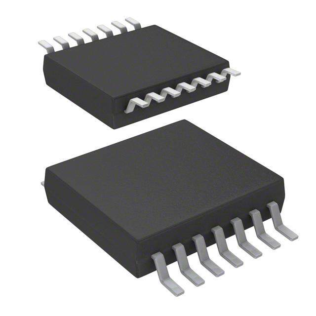
HCF40106YM013TR产品简介:
ICGOO电子元器件商城为您提供HCF40106YM013TR由STMicroelectronics设计生产,在icgoo商城现货销售,并且可以通过原厂、代理商等渠道进行代购。 HCF40106YM013TR价格参考¥1.50-¥1.50。STMicroelectronicsHCF40106YM013TR封装/规格:逻辑 - 栅极和逆变器, Inverter IC 6 Channel Schmitt Trigger 14-SO。您可以下载HCF40106YM013TR参考资料、Datasheet数据手册功能说明书,资料中有HCF40106YM013TR 详细功能的应用电路图电压和使用方法及教程。
HCF40106YM013TR是意法半导体(STMicroelectronics)生产的一款六路施密特触发反相器,属于逻辑门电路中的栅极和逆变器类别。该器件基于CMOS技术,具有高抗干扰能力和低功耗特性,广泛应用于各类电子系统中。

其主要应用场景包括:
1. 信号整形:由于内置施密特触发器,能有效对缓慢变化或带有噪声的输入信号进行整形,输出清晰的数字信号,常用于传感器信号调理电路。
2. 振荡电路:可构成RC振荡器,用于时钟信号生成、定时器或脉冲发生电路,适用于简单的频率源设计。
3. 开关去抖:在机械按键或开关输入电路中,用于消除触点抖动,提高系统可靠性,常见于工业控制面板和消费类电子产品。
4. 电平转换:支持宽电源电压范围(通常3V至15V),可用于不同电压逻辑系统之间的接口电平匹配。
5. 波形变换:将正弦波、三角波等模拟信号转换为方波,适用于测量仪器和通信设备中的前置处理电路。

该器件采用SO-14小型封装,适合高密度PCB布局,广泛用于工业控制、家用电器、汽车电子、仪器仪表及便携式设备中。凭借STMicroelectronics一贯的高可靠性和稳定性,HCF40106YM013TR在恶劣环境和长期运行场景下表现优异,是经典且实用的通用逻辑器件。
| 参数 | 数值 |
| 产品目录 | 集成电路 (IC)半导体 |
| 描述 | IC HEX SCHMITT TRIGGER 14SOIC变换器 Hex Schmitt Trigger Six Trigger Circuit |
| 产品分类 | |
| 品牌 | STMicroelectronics |
| 产品手册 | |
| 产品图片 |
|
| rohs | 符合RoHS无铅 / 符合限制有害物质指令(RoHS)规范要求 |
| 产品系列 | 逻辑集成电路,变换器,STMicroelectronics HCF40106YM013TR4000 |
| mouser_ship_limit | 该产品可能需要其他文件才能进口到中国。 |
| 数据手册 | |
| 产品型号 | HCF40106YM013TR |
| 不同V、最大CL时的最大传播延迟 | 120ns @ 15V,50pF |
| 产品种类 | 变换器 |
| 传播延迟时间 | 140 ns |
| 供应商器件封装 | 14-SO |
| 其它名称 | 497-14369-6 |
| 其它有关文件 | http://www.st.com/web/catalog/sense_power/FM140/SC1799/PF62997?referrer=70071840 |
| 包装 | Digi-Reel® |
| 商标 | STMicroelectronics |
| 安装类型 | 表面贴装 |
| 安装风格 | SMD/SMT |
| 封装 | Reel |
| 封装/外壳 | 14-SOIC(0.154",3.90mm 宽) |
| 封装/箱体 | SO-14 |
| 工作温度 | -55°C ~ 125°C |
| 工作温度范围 | - 40 C to + 125 C |
| 工厂包装数量 | 2500 |
| 最大工作温度 | + 125 C |
| 最小工作温度 | - 40 C |
| 标准包装 | 1 |
| 特性 | 施密特触发器 |
| 电压-电源 | 3 V ~ 20 V |
| 电流-输出高,低 | 6.8mA,6.8mA |
| 电流-静态(最大值) | 20µA |
| 电源电压-最大 | 20 V |
| 电源电压-最小 | 3 V |
| 电路数 | 6 |
| 电路数量 | 6 Circuit |
| 系列 | HCF40106 |
| 输入数 | 6 |
| 输入类型 | Schmitt Trigger |
| 输出类型 | Schmitt Trigger |
| 逻辑电平-低 | 0.9 V ~ 4 V |
| 逻辑电平-高 | 3.6 V ~ 10.8 V |
| 逻辑类型 | Hex Schmitt Inverter |
| 逻辑系列 | HCF |


- 商务部:美国ITC正式对集成电路等产品启动337调查
- 曝三星4nm工艺存在良率问题 高通将骁龙8 Gen1或转产台积电
- 太阳诱电将投资9.5亿元在常州建新厂生产MLCC 预计2023年完工
- 英特尔发布欧洲新工厂建设计划 深化IDM 2.0 战略
- 台积电先进制程称霸业界 有大客户加持明年业绩稳了
- 达到5530亿美元!SIA预计今年全球半导体销售额将创下新高
- 英特尔拟将自动驾驶子公司Mobileye上市 估值或超500亿美元
- 三星加码芯片和SET,合并消费电子和移动部门,撤换高东真等 CEO
- 三星电子宣布重大人事变动 还合并消费电子和移动部门
- 海关总署:前11个月进口集成电路产品价值2.52万亿元 增长14.8%


PDF Datasheet 数据手册内容提取
HCF40106 Hex Schmitt trigger Datasheet - production data Applications Automotive Industrial SO-14 Computer Consumer Features Description Schmitt trigger action with no external The HCF40106 is a monolithic integrated circuit components fabricated in metal oxide semiconductor Hysteresis voltage typically: technology available in an SO-14 package. 0.9 V at V = 5 V DD The HCF40106 consists of six Schmitt trigger 2.3 V at V =10 V DD circuits. Each circuit functions as an inverter with 3.5 V at V =15 V DD Schmitt trigger action on the input. The trigger Noise immunity greater than 50% switches at different points for positive and negative-going signals. The difference between No limit on input rise and fall times the positive voltage (V ) and the negative voltage P Low V to V current during slow input ramp DD SS (V ) is defined as hysteresis voltage (V ). N H Standardized symmetrical output characteristics Quiescent current specified up to 20 V 5 V, 10 V, and 15 V parametric ratings Input leakage current I = 100 nA (max.) at I V = 18 V and T = 25 C DD A 100% tested for quiescent current ESD performance – HBM: 2 kV – MM: 200 V – CDM: 1 kV Table 1. Device summary table Order code Temperature range Package Packing Marking HCF40106M013TR -55 ° C to +125 ° C SO-14 HCF40106 Tape & reel HCF40106YM013TR(1) -40 ° C to +125 ° C SO-14 HCF40106Y (automotive grade)(1) 1. Qualification and characterization according to AEC Q100 and Q003 or equivalent, advanced screening according to AEC Q001 and Q002 or equivalent. January 2014 DocID002017 Rev 4 1/16 This is information on a product in full production. www.st.com
Contents HCF40106 Contents 1 Pin information . . . . . . . . . . . . . . . . . . . . . . . . . . . . . . . . . . . . . . . . . . . . . 3 2 Functional description . . . . . . . . . . . . . . . . . . . . . . . . . . . . . . . . . . . . . . . 4 3 Electrical characteristics . . . . . . . . . . . . . . . . . . . . . . . . . . . . . . . . . . . . . 6 4 Typical applications . . . . . . . . . . . . . . . . . . . . . . . . . . . . . . . . . . . . . . . . 10 5 Package information . . . . . . . . . . . . . . . . . . . . . . . . . . . . . . . . . . . . . . . . 12 6 Ordering information . . . . . . . . . . . . . . . . . . . . . . . . . . . . . . . . . . . . . . . 15 7 Revision history . . . . . . . . . . . . . . . . . . . . . . . . . . . . . . . . . . . . . . . . . . . 15 2/16 DocID002017 Rev 4
HCF40106 Pin information 1 Pin information Figure 1. Pin connections (top view) (cid:36) (cid:20) (cid:20)(cid:23) (cid:57)(cid:39)(cid:39) (cid:42)(cid:3)(cid:32)(cid:3)(cid:36) (cid:21) (cid:20)(cid:22) (cid:41) (cid:37) (cid:22) (cid:20)(cid:21) (cid:47)(cid:3)(cid:32)(cid:3)(cid:41) (cid:43)(cid:3)(cid:32)(cid:3)(cid:37) (cid:23) (cid:20)(cid:20) (cid:40) (cid:38) (cid:24) (cid:20)(cid:19) (cid:46)(cid:3)(cid:32)(cid:3)(cid:40) (cid:44)(cid:3)(cid:32)(cid:3)(cid:38) (cid:25) (cid:28) (cid:39) (cid:57)(cid:54)(cid:54) (cid:26) (cid:27) (cid:45)(cid:3)(cid:32)(cid:3)(cid:39) (cid:42)(cid:36)(cid:48)(cid:54)(cid:20)(cid:24)(cid:19)(cid:21)(cid:20)(cid:22)(cid:20)(cid:19)(cid:24)(cid:21)(cid:38)(cid:37) Table 2. Pin description Pin no Symbol Name and function 1, 3, 5, 9, 11, 13 A, B, C, D, E, F Data inputs 2, 4, 6, 8, 10, 12 G, H, I, J, K, L Data outputs 7 V Negative supply voltage SS 14 V Positive supply voltage DD DocID002017 Rev 4 3/16 16
Functional description HCF40106 2 Functional description Figure 2. Logic diagram (cid:36)(cid:11)(cid:20)(cid:12)(cid:3) (cid:42) (cid:20)(cid:3)(cid:11)(cid:22)(cid:15)(cid:3)(cid:24)(cid:15)(cid:3)(cid:28)(cid:15)(cid:3)(cid:20)(cid:20)(cid:15)(cid:3)(cid:20)(cid:22)(cid:12) (cid:21)(cid:3)(cid:11)(cid:23)(cid:15)(cid:3)(cid:25)(cid:15)(cid:3)(cid:27)(cid:15)(cid:3)(cid:20)(cid:19)(cid:15)(cid:3)(cid:20)(cid:21)(cid:12) (cid:57)(cid:39)(cid:39) (cid:57)(cid:54)(cid:54) (cid:42)(cid:36)(cid:48)(cid:54)(cid:20)(cid:24)(cid:19)(cid:21)(cid:20)(cid:22)(cid:20)(cid:20)(cid:21)(cid:22)(cid:38)(cid:37)(cid:3) 1. All inputs protected by COS/MOS protection network. Table 3. Truth table Inputs (A to F) Outputs (G to L) L H H L Figure 3. Functional diagram (cid:20) (cid:21) (cid:36) (cid:42)(cid:3)(cid:32)(cid:3)(cid:36) (cid:22) (cid:23) (cid:37) (cid:43)(cid:3)(cid:32)(cid:3)(cid:37) (cid:24) (cid:25) (cid:38) (cid:44)(cid:3)(cid:32)(cid:3)(cid:38) (cid:28) (cid:27) (cid:39) (cid:45)(cid:3)(cid:32)(cid:3)(cid:39) (cid:20)(cid:20) (cid:20)(cid:19) (cid:40) (cid:46)(cid:3)(cid:32)(cid:3)(cid:40) (cid:20)(cid:22) (cid:20)(cid:21) (cid:41) (cid:47)(cid:3)(cid:32)(cid:3)(cid:41) (cid:57)(cid:39)(cid:39)(cid:3)(cid:32)(cid:3)(cid:20)(cid:23) (cid:42)(cid:36)(cid:48)(cid:54)(cid:20)(cid:24)(cid:19)(cid:21)(cid:20)(cid:22)(cid:20)(cid:22)(cid:19)(cid:19)(cid:38)(cid:37)(cid:3) (cid:57)(cid:54)(cid:54)(cid:3)(cid:32)(cid:3)(cid:26) 4/16 DocID002017 Rev 4
HCF40106 Functional description Figure 4. Input equivalent circuit (cid:57)(cid:39)(cid:39) (cid:44)(cid:49)(cid:51)(cid:56)(cid:55) (cid:57)(cid:54)(cid:54) (cid:42)(cid:36)(cid:48)(cid:54)(cid:21)(cid:23)(cid:19)(cid:20)(cid:20)(cid:22)(cid:20)(cid:20)(cid:20)(cid:22)(cid:38)(cid:37) DocID002017 Rev 4 5/16 16
Electrical characteristics HCF40106 3 Electrical characteristics Absolute maximum ratings are those values beyond which damage to the device may occur. Functional operation under these conditions is not implied. All voltage values are referred to V pin voltage. SS Table 4. Absolute maximum ratings (AMR) Symbol Parameter Value Unit V Supply voltage -0.5 to +22 DD V V DC input voltage -0.5 to V + 0.5 I DD I DC input current 10 mA I Power dissipation per package 200 P mW D Power dissipation per output transistor 100 T Operating temperature -55 to +125 op °C T Storage temperature -65 to +150 stg Table 5. Recommended operating conditions Symbol Parameter Value Unit V Supply voltage 3 to 20 DD V V Input voltage 0 to V I DD T Operating temperature -55 to 125 °C op 6/16 DocID002017 Rev 4
HCF40106 Electrical characteristics Table 6. DC specifications(1) Test condition Value Sym. Parameter T = 25 °C -40 to 85 °C -55 to 125 °C Unit A V (V) V (V) |I | (A) V (V) I O O DD Min. Typ. Max. Min. Max. Min. Max. 0/5 5 1 30 30 Quiescent 0/10 10 0.02 2 60 60 I A L current 0/15 15 4 120 120 0/20 20 0.04 20 600 600 0/5 5 4.95 4.95 4.95 High level V output 0/10 <1 10 9.95 9.95 9.95 OH voltage 0/15 15 14.95 14.95 14.95 5/0 5 Low level V output 10/0 <1 10 0.05 0.05 0.05 OL voltage 15/0 15 Positive 5 2.2 2.9 3.6 2.2 3.6 2.2 3.6 trigger V 10 4.6 5.9 7.1 4.6 7.1 4.6 7.1 V P threshold voltage 15 6.8 8.8 10.8 6.8 10.8 6.8 10.8 Negative 5 0.9 1.9 2.8 0.9 2.8 0.9 2.8 trigger V 10 2.5 3.9 5.2 2.5 5.2 2.5 5.2 N threshold voltage 15 4 5.8 7.4 4 7.4 4 7.4 5 0.3 0.9 1.6 0.3 1.6 0.3 1.6 Hysteresis V 10 1.2 2.3 3.4 1.2 3.4 1.2 3.4 H voltage 15 1.6 3.5 5 1.6 5 1.6 5 2.5 -1.36 -3.2 -1.15 -1.1 0/5 5 Output 4.6 -0.44 -1 -0.36 -0.36 I drive mA OH current 0/10 9.5 10 -1.1 -2.6 -0.9 -0.9 0/15 13.5 15 -3.0 -6.8 -2.4 -2.4 0/5 0.4 5 0.44 1 0.36 0.36 Output sink I 0/10 0.5 10 1.1 2.6 0.9 0.9 mA OL current 0/15 1.5 15 3.0 6.8 2.4 2.4 Input I leakage 0/18 Any input 18 10-5 0.1 1 1 A I current Input C Any input 5 7.5 pF I capacitance 1. The noise margin for both level "1" and "0" is: 1 V min. with V = 5 V, 2 V min. with V = 10 V, and 2.5 V min. with DD DD V = 15 V. DD DocID002017 Rev 4 7/16 16
Electrical characteristics HCF40106 Table 7. Dynamic electrical characteristics (T = 25 °C, C = 50 pF, R = 200 k, t = t = 20 ns) amb L L r f Test condition Value(1) Symbol Parameter Unit V (V) Typ. Max. DD 5 140 280 t , t Propagation delay time 10 70 140 PLH PHL 15 60 120 ns 5 100 200 t , t Output transition time 10 50 100 TLH THL 15 40 80 1. The typical temperature coefficient for all V values is 0.3 %/°C. DD Figure 5. Test circuit (cid:57) (cid:39)(cid:39) (cid:51)(cid:88)(cid:79)(cid:86)(cid:72)(cid:3)(cid:74)(cid:72)(cid:81)(cid:72)(cid:85)(cid:68)(cid:87)(cid:82)(cid:85) (cid:39)(cid:56)(cid:55) (cid:53)(cid:55) (cid:57)(cid:54)(cid:54) (cid:38)(cid:47) (cid:53)(cid:47) (cid:42)(cid:36)(cid:48)(cid:54)(cid:19)(cid:23)(cid:19)(cid:21)(cid:20)(cid:22)(cid:20)(cid:25)(cid:21)(cid:25)(cid:38)(cid:37) 1. Legend: C = 50 pF or equivalent (includes jig and probe capacitance), R = 200 KR = Z of pulse L L T OUT generator (typically 50 ) 8/16 DocID002017 Rev 4
HCF40106 Electrical characteristics Figure 6. Propagation delay time waveform (f = 1 MHz; 50 % duty cycle) (cid:21)(cid:19)(cid:3)(cid:81)(cid:86) (cid:21)(cid:19)(cid:3)(cid:81)(cid:86) (cid:57) (cid:28)(cid:19)(cid:3)(cid:8) (cid:39)(cid:39) (cid:44)(cid:49)(cid:3) (cid:24)(cid:19)(cid:3)(cid:8) (cid:24)(cid:19)(cid:3)(cid:8) (cid:20)(cid:19)(cid:3)(cid:8) (cid:57) (cid:54)(cid:54) (cid:50)(cid:56)(cid:55)(cid:3) (cid:87) (cid:87) (cid:51)(cid:43)(cid:47) (cid:51)(cid:47)(cid:43) (cid:57) (cid:28)(cid:19)(cid:3)(cid:8) (cid:28)(cid:19)(cid:3)(cid:8) (cid:50)(cid:43) (cid:24)(cid:19)(cid:3)(cid:8) (cid:24)(cid:19)(cid:3)(cid:8) (cid:20)(cid:19)(cid:3)(cid:8) (cid:20)(cid:19)(cid:3)(cid:8) (cid:57) (cid:50)(cid:47) (cid:87) (cid:87) (cid:55)(cid:43)(cid:47) (cid:55)(cid:47)(cid:43) (cid:42)(cid:36)(cid:48)(cid:54)(cid:20)(cid:22)(cid:19)(cid:21)(cid:20)(cid:22)(cid:20)(cid:25)(cid:20)(cid:25)(cid:38)(cid:37) DocID002017 Rev 4 9/16 16
Typical applications HCF40106 4 Typical applications Figure 7. Astable multivibrator (cid:20)(cid:18)(cid:25)(cid:3)(cid:43)(cid:38)(cid:41)(cid:23)(cid:19)(cid:20)(cid:19)(cid:25) (cid:57)(cid:54)(cid:54) (cid:87)(cid:36) (cid:57)(cid:39)(cid:39) (cid:53) (cid:57)(cid:54)(cid:54) (cid:38) (cid:57)(cid:54)(cid:54) (cid:42)(cid:36)(cid:48)(cid:54)(cid:20)(cid:24)(cid:19)(cid:21)(cid:20)(cid:22)(cid:20)(cid:23)(cid:22)(cid:19)(cid:38)(cid:37)(cid:3) V V –V t = RCln -----P-------D---D--------------N-- A V V –V N DD P 50 k R 1 m 100 pF C 1 F For the range of R and C given 2 s < t < 0.4 s A Figure 8. Monostable multivibrator (cid:57)(cid:39)(cid:39) (cid:87)(cid:48) (cid:57)(cid:39)(cid:39) (cid:53) (cid:57)(cid:54)(cid:54) (cid:57)(cid:39)(cid:39) (cid:20) (cid:21) (cid:57)(cid:54)(cid:54) (cid:38) (cid:20)(cid:18)(cid:25)(cid:3)(cid:43)(cid:38)(cid:41)(cid:23)(cid:19)(cid:20)(cid:19)(cid:25) (cid:20)(cid:18)(cid:22)(cid:3)(cid:43)(cid:38)(cid:41)(cid:23)(cid:19)(cid:19)(cid:26)(cid:56) (cid:57)(cid:54)(cid:54) (cid:42)(cid:36)(cid:48)(cid:54)(cid:20)(cid:24)(cid:19)(cid:21)(cid:20)(cid:22)(cid:20)(cid:24)(cid:19)(cid:19)(cid:38)(cid:37)(cid:3) V t = RCln-----------D----D--------- M V –V DD P 50 k R 1 m 100 pF C 1 F For the range of R and C given 5 s < t < 1s M 10/16 DocID002017 Rev 4
HCF40106 Typical applications Figure 9. Wave sharper (cid:57)(cid:39)(cid:39) (cid:57)(cid:39)(cid:39) (cid:57)(cid:54)(cid:54) (cid:57)(cid:54)(cid:54) (cid:20)(cid:18)(cid:25)(cid:3)(cid:43)(cid:38)(cid:41)(cid:23)(cid:19)(cid:20)(cid:19)(cid:25) (cid:42)(cid:36)(cid:48)(cid:54)(cid:20)(cid:24)(cid:19)(cid:21)(cid:20)(cid:22)(cid:20)(cid:24)(cid:22)(cid:19)(cid:38)(cid:37)(cid:3) The frequency range of the wave shape is from DC to 1 MHz. DocID002017 Rev 4 11/16 16
Package information HCF40106 5 Package information In order to meet environmental requirements, ST offers these devices in different grades of ECOPACK® packages, depending on their level of environmental compliance. ECOPACK® specifications, grade definitions and product status are available at: www.st.com. ECOPACK® is an ST trademark. 12/16 DocID002017 Rev 4
HCF40106 Package information Figure 10. SO-14 package mechanical drawing (cid:47) (cid:42) (cid:38) (cid:70)(cid:20) (cid:68)(cid:21) (cid:36) (cid:69) (cid:72) (cid:68)(cid:20) (cid:69)(cid:20) (cid:54) (cid:72)(cid:22) (cid:40) (cid:39) (cid:48) (cid:20)(cid:23) (cid:27) (cid:41) (cid:20) (cid:26) (cid:42)(cid:36)(cid:48)(cid:54)(cid:19)(cid:24)(cid:19)(cid:21)(cid:20)(cid:22)(cid:20)(cid:19)(cid:21)(cid:26)(cid:38)(cid:37) Table 8. SO-14 package mechanical data Dimensions Ref Millimeters Inches Min. Typ. Max. Min. Typ. Max. A 1.75 0.068 a1 0.1 0.2 0.003 0.007 a2 1.65 0.064 b 0.35 0.46 0.013 0.018 b1 0.19 0.25 0.007 0.010 C 0.5 0.019 c1 45 45 D 8.55 8.75 0.336 0.344 E 5.8 6.2 0.228 0.244 e 1.27 0.050 e3 7.62 0.300 F 3.8 4.0 0.149 0.157 G 4.6 5.3 0.181 0.208 L 0.5 1.27 0.019 0.050 M 0.68 0.026 S 8 8 DocID002017 Rev 4 13/16 16
Package information HCF40106 Figure 11. SO-14 tape and reel information (cid:49) (cid:39) (cid:38) (cid:36) (cid:55) (cid:51)(cid:82) (cid:37)(cid:82) (cid:51) (cid:46)(cid:82) (cid:36)(cid:82) (cid:42)(cid:36)(cid:48)(cid:54)(cid:20)(cid:21)(cid:19)(cid:21)(cid:20)(cid:22)(cid:20)(cid:25)(cid:21)(cid:21)(cid:38)(cid:37) 1. Drawing is not to scale. Table 9. SO-14 tape and reel information Dimensions Ref Millimeters Inches Min. Typ. Max. Min. Typ. Max. A 330 12.992 C 12.8 13.2 0.504 0.519 D 20.2 0.795 N 60 2.362 T 22.4 0.882 Ao 6.4 6.6 0.252 0.260 Bo 9 9.2 0.354 0.362 Ko 2.1 2.3 0.082 0.090 Po 3.9 4.1 0.153 0.161 P 7.9 8.1 0.311 0.319 14/16 DocID002017 Rev 4
HCF40106 Ordering information 6 Ordering information Table 10. Order codes Order code Temperature range Package Packing Marking HCF40106M013TR -55 ° C to +125 ° C SO-14 HCF40106 Tape & HCF40106YM013TR(1) -40 ° C to +125 ° C SO-14 reel HCF40106Y (automotive grade)(1) 1. Qualification and characterization according to AEC Q100 and Q003 or equivalent, advanced screening according to AEC Q001 and Q002 or equivalent. 7 Revision history Table 11. Document revision history Date Revision Changes Document template and layout updated Updated package names (PDIP-14 and SO-14 instead of DIP-14 and SOP-14) Updated Features 19-Feb-2013 3 Added Applications Updated Device summary table Removed “HCC” from Figure 7, Figure 8, and Figure 9 Added Section 6: Ordering information Removed DIP package option Added ESD performance to Features 06-Jan-2014 4 Updated footnote 1 of Table 1: Device summary table Updated footnote 1 of Table 10: Order codes DocID002017 Rev 4 15/16 16
HCF40106 Please Read Carefully: Information in this document is provided solely in connection with ST products. STMicroelectronics NV and its subsidiaries (“ST”) reserve the right to make changes, corrections, modifications or improvements, to this document, and the products and services described herein at any time, without notice. All ST products are sold pursuant to ST’s terms and conditions of sale. Purchasers are solely responsible for the choice, selection and use of the ST products and services described herein, and ST assumes no liability whatsoever relating to the choice, selection or use of the ST products and services described herein. No license, express or implied, by estoppel or otherwise, to any intellectual property rights is granted under this document. If any part of this document refers to any third party products or services it shall not be deemed a license grant by ST for the use of such third party products or services, or any intellectual property contained therein or considered as a warranty covering the use in any manner whatsoever of such third party products or services or any intellectual property contained therein. UNLESS OTHERWISE SET FORTH IN ST’S TERMS AND CONDITIONS OF SALE ST DISCLAIMS ANY EXPRESS OR IMPLIED WARRANTY WITH RESPECT TO THE USE AND/OR SALE OF ST PRODUCTS INCLUDING WITHOUT LIMITATION IMPLIED WARRANTIES OF MERCHANTABILITY, FITNESS FOR A PARTICULAR PURPOSE (AND THEIR EQUIVALENTS UNDER THE LAWS OF ANY JURISDICTION), OR INFRINGEMENT OF ANY PATENT, COPYRIGHT OR OTHER INTELLECTUAL PROPERTY RIGHT. ST PRODUCTS ARE NOT DESIGNED OR AUTHORIZED FOR USE IN: (A) SAFETY CRITICAL APPLICATIONS SUCH AS LIFE SUPPORTING, ACTIVE IMPLANTED DEVICES OR SYSTEMS WITH PRODUCT FUNCTIONAL SAFETY REQUIREMENTS; (B) AERONAUTIC APPLICATIONS; (C) AUTOMOTIVE APPLICATIONS OR ENVIRONMENTS, AND/OR (D) AEROSPACE APPLICATIONS OR ENVIRONMENTS. WHERE ST PRODUCTS ARE NOT DESIGNED FOR SUCH USE, THE PURCHASER SHALL USE PRODUCTS AT PURCHASER’S SOLE RISK, EVEN IF ST HAS BEEN INFORMED IN WRITING OF SUCH USAGE, UNLESS A PRODUCT IS EXPRESSLY DESIGNATED BY ST AS BEING INTENDED FOR “AUTOMOTIVE, AUTOMOTIVE SAFETY OR MEDICAL” INDUSTRY DOMAINS ACCORDING TO ST PRODUCT DESIGN SPECIFICATIONS. PRODUCTS FORMALLY ESCC, QML OR JAN QUALIFIED ARE DEEMED SUITABLE FOR USE IN AEROSPACE BY THE CORRESPONDING GOVERNMENTAL AGENCY. Resale of ST products with provisions different from the statements and/or technical features set forth in this document shall immediately void any warranty granted by ST for the ST product or service described herein and shall not create or extend in any manner whatsoever, any liability of ST. ST and the ST logo are trademarks or registered trademarks of ST in various countries. Information in this document supersedes and replaces all information previously supplied. The ST logo is a registered trademark of STMicroelectronics. All other names are the property of their respective owners. © 2014 STMicroelectronics - All rights reserved STMicroelectronics group of companies Australia - Belgium - Brazil - Canada - China - Czech Republic - Finland - France - Germany - Hong Kong - India - Israel - Italy - Japan - Malaysia - Malta - Morocco - Philippines - Singapore - Spain - Sweden - Switzerland - United Kingdom - United States of America www.st.com 16/16 DocID002017 Rev 4
Mouser Electronics Authorized Distributor Click to View Pricing, Inventory, Delivery & Lifecycle Information: S TMicroelectronics: HCF40106BEY HCF40106BM1 HCF40106M013TR HCF40106YM013TR