ICGOO在线商城 > 集成电路(IC) > 逻辑器件 - 转换器,电平移位器 > GTL2010BS,118
 Datasheet下载
- 型号: GTL2010BS,118
- 制造商: NXP Semiconductors
- 库位|库存: xxxx|xxxx
- 要求:
| 数量阶梯 | 香港交货 | 国内含税 |
| +xxxx | $xxxx | ¥xxxx |
查看当月历史价格
查看今年历史价格
GTL2010BS,118产品简介:
ICGOO电子元器件商城为您提供GTL2010BS,118由NXP Semiconductors设计生产,在icgoo商城现货销售,并且可以通过原厂、代理商等渠道进行代购。 GTL2010BS,118价格参考。NXP SemiconductorsGTL2010BS,118封装/规格:逻辑器件 - 转换器,电平移位器, Voltage Level Translator Bidirectional 1 Circuit 10 Channel 24-HVQFN (4x4)。您可以下载GTL2010BS,118参考资料、Datasheet数据手册功能说明书,资料中有GTL2010BS,118 详细功能的应用电路图电压和使用方法及教程。
NXP USA Inc. 生产的 GTL2010BS,118 是一款逻辑器件,属于转换器和电平移位器类别。它主要用于在不同电压电平的数字信号之间进行转换,确保信号的正确传输和处理。以下是该型号的一些应用场景:

 1. 多电压系统中的信号转换
   在现代电子系统中,不同模块可能工作在不同的电压电平(如3.3V、5V等)。GTL2010BS,118 可以在这些不同电压电平之间进行双向转换,确保信号的完整性。例如,在一个包含微控制器(3.3V)和外设(5V)的系统中,该器件可以确保两者之间的通信不会因为电压差异而出现问题。

 2. 高速数据传输
   GTL2010BS,118 支持高速数据传输,适用于需要高带宽的应用场景,如工业自动化、通信设备、网络接口卡等。它可以确保在高速数据传输过程中,信号的稳定性和准确性,避免因电压不匹配导致的数据丢失或错误。

 3. 低功耗设计
   该器件具有较低的静态电流消耗,适合用于对功耗敏感的应用,如便携式设备、电池供电的传感器节点等。通过优化功耗,GTL2010BS,118 可以延长设备的续航时间,同时保持高效的信号转换能力。

 4. 工业控制与自动化
   在工业控制系统中,GTL2010BS,118 可以用于连接不同电压电平的传感器、执行器和控制器。例如,在工厂自动化环境中,PLC(可编程逻辑控制器)可能工作在一种电压电平,而传感器或执行器可能使用不同的电压电平。该器件可以确保这些设备之间的可靠通信,提升系统的稳定性和可靠性。

 5. 消费电子产品
   在消费电子产品中,如智能手机、平板电脑和其他便携式设备中,GTL2010BS,118 可以用于内部不同模块之间的电压转换。例如,将来自外部接口(如USB)的5V信号转换为内部电路所需的3.3V信号,或者反之亦然。

 6. 汽车电子
   汽车电子系统中,不同模块可能工作在不同的电压电平,特别是在涉及到电源管理、传感器接口和通信总线的情况下。GTL2010BS,118 可以确保这些模块之间的信号兼容性,尤其是在CAN总线、LIN总线等通信协议中,确保信号的可靠传输。

总之,GTL2010BS,118 是一款适用于多种应用场景的高性能电平移位器,特别适合需要在不同电压电平之间进行高效、可靠的信号转换的系统。
| 参数 | 数值 |
| 产品目录 | 集成电路 (IC)半导体 |
| 描述 | IC VOLT TRANSLATOR 24-HVQFN转换 - 电压电平 VOLT TRANSLATOR |
| 产品分类 | 逻辑 - 变换器集成电路 - IC |
| 品牌 | NXP Semiconductors |
| 产品手册 | |
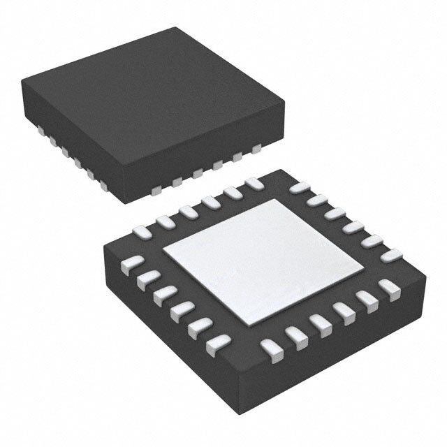
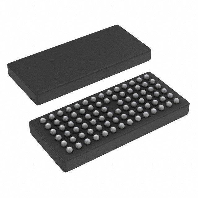
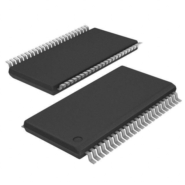
| 产品图片 |
|
| rohs | 符合RoHS无铅 / 符合限制有害物质指令(RoHS)规范要求 |
| 产品系列 | 逻辑集成电路,转换 - 电压电平,NXP Semiconductors GTL2010BS,118- |
| 数据手册 | |
| 产品型号 | GTL2010BS,118 |
| PCN封装 | |
| 产品培训模块 | http://www.digikey.cn/PTM/IndividualPTM.page?site=cn&lang=zhs&ptm=24983 |
| 产品目录页面 | |
| 产品种类 | 转换 - 电压电平 |
| 传播延迟(最大值) | 1.5ns |
| 位数 | 10 |
| 供应商器件封装 | 24-HVQFN(4x4) |
| 其它名称 | 568-3632-2 |
| 包装 | 带卷 (TR) |
| 商标 | NXP Semiconductors |
| 安装类型 | 表面贴装 |
| 安装风格 | SMD/SMT |
| 封装 | Reel |
| 封装/外壳 | 24-VFQFN 裸露焊盘 |
| 封装/箱体 | SOT-616 |
| 工作温度 | -40°C ~ 85°C |
| 工厂包装数量 | 6000 |
| 差分-输入:输出 | 无/无 |
| 数据速率 | - |
| 最大工作温度 | + 85 C |
| 最小工作温度 | - 40 C |
| 标准包装 | 6,000 |
| 特色产品 | http://www.digikey.com/cn/zh/ph/NXP/I2C.html |
| 电压-电源 | 2.36 V ~ 2.64 V,3 V ~ 3.6 V |
| 电源电压-最大 | 2.64 V, 3.6 V |
| 电源电压-最小 | 2.36 V, 3 V |
| 输入类型 | GTL |
| 输出/通道数 | 1 |
| 输出类型 | LVTTL,TTL |
| 通道数 | 10 |
| 逻辑功能 | 变换器,双向,开路漏极 |
| 零件号别名 | GTL2010BS-T |


- 商务部:美国ITC正式对集成电路等产品启动337调查
- 曝三星4nm工艺存在良率问题 高通将骁龙8 Gen1或转产台积电
- 太阳诱电将投资9.5亿元在常州建新厂生产MLCC 预计2023年完工
- 英特尔发布欧洲新工厂建设计划 深化IDM 2.0 战略
- 台积电先进制程称霸业界 有大客户加持明年业绩稳了
- 达到5530亿美元!SIA预计今年全球半导体销售额将创下新高
- 英特尔拟将自动驾驶子公司Mobileye上市 估值或超500亿美元
- 三星加码芯片和SET,合并消费电子和移动部门,撤换高东真等 CEO
- 三星电子宣布重大人事变动 还合并消费电子和移动部门
- 海关总署:前11个月进口集成电路产品价值2.52万亿元 增长14.8%


PDF Datasheet 数据手册内容提取
GTL2010 10-bit bidirectional low voltage translator Rev. 06 — 3 March 2008 Product data sheet 1. General description The Gunning Transceiver Logic - Transceiver Voltage Clamps (GTL-TVC) provide high-speed voltage translation with low ON-state resistance and minimal propagation delay.TheGTL2010provides10NMOSpasstransistors(SnandDn)withacommongate (GREF) and a reference transistor (SREF and DREF). The device allows bidirectional voltage translations between 1.0V and 5.0V without use of a direction pin. When the Sn or Dn port is LOW, the clamp is in the ON-state and a low resistance connectionexistsbetweentheSnandDnports.AssumingthehighervoltageisontheDn port, when the Dn port is HIGH the voltage on the Sn port is limited to the voltage set by thereferencetransistor(SREF).WhentheSnportisHIGH,theDnportispulledtoV by CC the pull-up resistors. This functionality allows a seamless translation between higher and lower voltages selected by the user, without the need for directional control. Alltransistorshavethesameelectricalcharacteristicsandthereisminimaldeviationfrom one output to another in voltage or propagation delay. This is a benefit over discrete transistor voltage translation solutions, since the fabrication of the transistors is symmetrical. Because all transistors in the device are identical, SREF and DREF can be located on any of the other ten matched Sn/Dn transistors, allowing for easier board layout. The translator's transistors provide excellent ESD protection to lower voltage devices and at the same time protect less ESD-resistant devices. 2. Features n 10-bit bidirectional low voltage translator n Allowsvoltageleveltranslationbetween1.0V,1.2V,1.5V,1.8V,2.5V,3.3V,and5V buses,whichallowsdirectinterfacewithGTL,GTL+,LVTTL/TTLand5VCMOSlevels n Provides bidirectional voltage translation with no direction pin n Low 6.5W ON-state resistance (R ) between input and output pins (Sn/Dn) on n Supports hot insertion n No power supply required: will not latch up n 5V tolerant inputs n Low standby current n Flow-through pinout for ease of printed-circuit board trace routing n ESD protection exceeds 2000V HBM per JESD22-A114, 200V MM per JESD22-A115, and 1000V CDM per JESD22-C101 n Packages offered: TSSOP24, HVQFN24
GTL2010 NXP Semiconductors 10-bit bidirectional low voltage translator 3. Applications n Any application that requires bidirectional or unidirectional voltage level translation from any voltage from 1.0V to 5.0V to any voltage from 1.0V to 5.0V n The open-drain construction with no direction pin is ideal for bidirectional low voltage (for example, 1.0V, 1.2V, 1.5V or 1.8V) processor I2C-bus port translation to the normal3.3Vand/or5.0VI2C-bussignallevelsorGTL/GTL+translationtoLVTTL/TTL signal levels 4. Ordering information Table 1. Ordering information Type number Package Name Description Version GTL2010PW TSSOP24 plastic thin shrink small outline package; 24leads; SOT355-1 bodywidth4.4mm GTL2010BS HVQFN24 plasticthermalenhancedverythinquadflatpackage; SOT616-1 noleads; 24terminals; body4· 4· 0.85mm 4.1 Ordering options Table 2. Ordering options Type number Topside mark Temperature range GTL2010PW GTL2010 - 40(cid:176) C to +85(cid:176) C GTL2010BS 2010 - 40(cid:176) C to +85(cid:176) C 5. Functional diagram DREF GREF D1 D10 SREF S1 S10 002aac059 Fig 1. Functional diagram GTL2010_6 © NXP B.V. 2008. All rights reserved. Product data sheet Rev. 06 — 3 March 2008 2 of 20
GTL2010 NXP Semiconductors 10-bit bidirectional low voltage translator 6. Pinning information 6.1 Pinning GND 1 24 GREF EF D EF EF terminal 1 1 R N R R 1 SREF 2 23 DREF S S G G D D index area S1 3 22 D1 24 23 22 21 20 19 S2 4 21 D2 S2 1 18 D2 S3 5 20 D3 S3 2 17 D3 S4 6 19 D4 S4 3 16 D4 GTL2010PW GTL2010BS S5 7 18 D5 S5 4 15 D5 S6 8 17 D6 S6 5 14 D6 S7 9 16 D7 S7 6 13 D7 S8 10 15 D8 7 8 9 10 11 12 S9 11 14 D9 8 9 0 0 9 8 S10 12 13 D10 S S S1 D1 D D 002aac058 002aac057 Transparent top view Fig 2. Pin configuration for TSSOP24 Fig 3. Pin configuration for HVQFN24 6.2 Pin description Table 3. Pin description Symbol Pin Description TSSOP24 HVQFN24 GND 1 22[1] ground (0V) SREF 2 23 source of reference transistor S1 to S10 3, 4, 5, 6, 7, 8, 9, 24,1,2,3,4,5,6, Port S1 to Port S10 10, 11, 12 7, 8, 9 D1 to D10 22,21,20,19,18, 19,18,17,16,15, Port D1 to Port D10 17, 16, 15, 14, 13 14, 13, 12, 11, 10 DREF 23 20 drain of reference transistor GREF 24 21 gate of reference transistor [1] HVQFN24 package die supply ground is connected to both GND pin and exposed center pad. GND pin must be connected to supply ground for proper device operation. For enhanced thermal, electrical, and board level performance, the exposed pad needs to be soldered to the board using a corresponding thermal pad on the board and for proper heat conduction through the board, thermal vias need to be incorporated in the printed-circuit board in the thermal pad region. GTL2010_6 © NXP B.V. 2008. All rights reserved. Product data sheet Rev. 06 — 3 March 2008 3 of 20
GTL2010 NXP Semiconductors 10-bit bidirectional low voltage translator 7. Functional description Refer also toFigure 1 “Functional diagram”. 7.1 Function selection Table 4. Function selection, HIGH-to-LOW translation Assumes Dn is at the higher voltage level. H=HIGH voltage level; L=LOW voltage level; X=Don’t care GREF[1] DREF SREF[2] Input Dn Output Sn Transistor H H 0V X X off H H V H V [3] on T T H H V L L[4] on T L L 0V- V X X off T [1] GREF should be at least 1.5V higher than SREF for best translator operation. [2] V is equal to the SREF voltage. T [3] Sn is not pulled up or pulled down. [4] Sn follows the Dn input LOW. Table 5. Function selection, LOW-to-HIGH translation Assumes Dn is at the higher voltage level. H=HIGH voltage level; L=LOW voltage level; X=Don’t care GREF[1] DREF SREF[2] Input Sn Output Dn Transistor H H 0V X X off H H V V H[3] nearly off T T H H V L L[4] on T L L 0V- V X X off T [1] GREF should be at least 1.5V higher than SREF for best translator operation. [2] V is equal to the SREF voltage. T [3] Dn is pulled up to V through an external resistor. CC [4] Dn follows the Sn input LOW. GTL2010_6 © NXP B.V. 2008. All rights reserved. Product data sheet Rev. 06 — 3 March 2008 4 of 20
GTL2010 NXP Semiconductors 10-bit bidirectional low voltage translator 8. Application design-in information 8.1 Bidirectional translation For the bidirectional clamping configuration, higher voltage to lower voltage or lower voltage to higher voltage, the GREF input must be connected to DREF and both pins pulled to HIGH side V through a pull-up resistor (typically 200kW ). A filter capacitor on CC DREF is recommended. The processor output can be totem pole or open-drain (pull-up resistors may be required) and the chipset output can be totem pole or open-drain (pull-up resistors are required to pull the Dn outputs to V ). However, if either output is CC totempole,datamustbeunidirectionalortheoutputsmustbe3-stateableandtheoutputs must be controlled by some direction control mechanism to prevent HIGH-to-LOW contentions in either direction. If both outputs are open-drain, no direction control is needed. The opposite side of the reference transistor (SREF) is connected to the processorcorepowersupplyvoltage.WhenDREFisconnectedthrougha200kW resistor toa3.3Vto5.5VV supplyandSREFissetbetween1.0Vto(V - 1.5V),theoutput CC CC of each Sn has a maximum output voltage equal to SREF and the output of each Dn has a maximum output voltage equal to V . CC 1.8 V 5 V 1.5 V 1.2 V 200 kW totem pole or 1.0 V open-drain I/O GND GREF VCORE SREF DREF VCC S1 D1 CPU I/O CHIPSET I/O S2 D2 increase bit size 3.3 V by using 10-bit GTL2010 or 22-bit GTL2000 VCC S3 D3 CHIPSET I/O S4 D4 S5 D5 Sn Dn 002aac060 Typical bidirectional voltage translation. Fig 4. Bidirectional translation to multiple higher voltage levels such as an I2C-bus application GTL2010_6 © NXP B.V. 2008. All rights reserved. Product data sheet Rev. 06 — 3 March 2008 5 of 20
GTL2010 NXP Semiconductors 10-bit bidirectional low voltage translator 8.2 Unidirectional down translation For unidirectional clamping, higher voltage to lower voltage, the GREF input must be connectedtoDREFandbothpinspulledtothehighersideV throughapull-upresistor CC (typically 200kW ). A filter capacitor on DREF is recommended. Pull-up resistors are required if the chipset I/Os are open-drain. The opposite side of the reference transistor (SREF) is connected to the processor core supply voltage. When DREF is connected through a 200kW resistor to a 3.3V to 5.5V V supply and SREF is set between 1.0V CC to (V - 1.5V), the output of each Sn has a maximum output voltage equal to SREF. CC 1.8 V 5 V 1.5 V 1.2 V 200 kW 1.0 V easy migration to lower voltage as processor geometry shrinks GND GREF VCORE SREF DREF VCC S1 D1 CPU I/O CHIPSET I/O S2 D2 totem pole I/O 002aac061 Typical unidirectional HIGH-to-LOW voltage translation. Fig 5. Unidirectional down translation to protect low voltage processor pins 8.3 Unidirectional up translation Forunidirectionaluptranslation,lowervoltagetohighervoltage,thereferencetransistoris connectedthesameasforadowntranslation.Apull-upresistorisrequiredonthehigher voltageside(DnorSn)togetthefullHIGHlevel,sincetheGTL-TVCdevicewillonlypass thereferencesource(SREF)voltageasaHIGHwhendoinganuptranslation.Thedriver on the lower voltage side only needs pull-up resistors if it is open-drain. 1.8 V 5 V 1.5 V 1.2 V 200 kW 1.0 V easy migration to lower voltage as processor geometry shrinks GND GREF VCORE SREF DREF VCC S1 D1 CPU I/O CHIPSET I/O S2 D2 totem pole I/O or open-drain 002aac062 Typical unidirectional LOW-to-HIGH voltage translation. Fig 6. Unidirectional down translation to protect low voltage processor pins GTL2010_6 © NXP B.V. 2008. All rights reserved. Product data sheet Rev. 06 — 3 March 2008 6 of 20
GTL2010 NXP Semiconductors 10-bit bidirectional low voltage translator 8.4 Sizing pull-up resistor The pull-up resistor value needs to limit the current through the pass transistor when it is in the ‘on’ state to about 15mA. This will guarantee a pass voltage of 260mV to 350mV. If the current through the pass transistor is higher than 15mA, the pass voltage will also be higher in the ‘on’ state. To set the current through each pass transistor at 15mA, the pull-up resistor value is calculated as shown inEquation1: pull-up voltage (V)– 0.35 V resistor value (W ) = ------------------------------------------------------------------------------- (1) 0.015 A Table6 summarizes resistor values for various reference voltages and currents at 15mA and also at 10mA and 3mA. The resistor value shown in the +10% column or a larger valueshouldbeusedtoensurethatthepassvoltageofthetransistorwouldbe350mVor less. The external driver must be able to sink the total current from the resistors on both sides of the GTL-TVC device at 0.175V, although the 15mA only applies to current flowing through the GTL-TVC device. See application noteAN10145, “Bi-directional low voltage translators” for more information. Table 6. Pull-up resistor values Voltage Pull-up resistor value (W )[1] 15mA[2] 10mA[2] 3mA[2] Nominal +10%[3] Nominal +10%[3] Nominal +10%[3] 5.0V 310 341 465 512 1550 1705 3.3V 197 217 295 325 983 1082 2.5V 143 158 215 237 717 788 1.8V 97 106 145 160 483 532 1.5V 77 85 115 127 383 422 1.2V 57 63 85 94 283 312 [1] Calculated for V =0.35V. OL [2] Assumes output driver V =0.175 V at stated current. OL [3] +10% to compensate for V range and resistor tolerance. CC GTL2010_6 © NXP B.V. 2008. All rights reserved. Product data sheet Rev. 06 — 3 March 2008 7 of 20
GTL2010 NXP Semiconductors 10-bit bidirectional low voltage translator 9. Limiting values Table 7. Limiting values[1] In accordance with the Absolute Maximum Rating System (IEC 60134). Symbol Parameter Conditions Min Max Unit V voltage on pin SREF [2] - 0.5 +7.0 V SREF V voltage on pin DREF [2] - 0.5 +7.0 V DREF V voltage on pin GREF [2] - 0.5 +7.0 V GREF V voltage on port Sn [2] - 0.5 +7.0 V Sn V voltage on port Dn [2] - 0.5 +7.0 V Dn I diode current on reference pins V <0V - - 50 mA REFK I I diode current Port Sn V <0V - - 50 mA SK I I diode current Port Dn V <0V - - 50 mA DK I I clamp current per channel channel in - – 128 mA MAX ON-state T storage temperature - 65 +150 (cid:176) C stg [1] The performance capability of a high-performance integrated circuit in conjunction with its thermal environment can create junction temperatures which are detrimental to reliability. The maximum junction temperature of this integrated circuit should not exceed 150(cid:176) C. [2] Theinputandoutputnegativevoltageratingsmaybeexceedediftheinputandoutputclampcurrentratings are observed. 10. Recommended operating conditions Table 8. Recommended operating conditions Symbol Parameter Conditions Min Typ Max Unit V voltage on an input/output pin Sn, Dn 0 - 5.5 V I/O V voltage on pin SREF [1] 0 - 5.5 V SREF V voltage on pin DREF 0 - 5.5 V DREF V voltage on pin GREF 0 - 5.5 V GREF I pass transistor current - - 64 mA PASS T ambient temperature operating in free air - 40 - +85 (cid:176) C amb [1] V £ V - 1.5V for best results in level shifting applications. SREF DREF GTL2010_6 © NXP B.V. 2008. All rights reserved. Product data sheet Rev. 06 — 3 March 2008 8 of 20
GTL2010 NXP Semiconductors 10-bit bidirectional low voltage translator 11. Static characteristics Table 9. Static characteristics T =- 40(cid:176) C to +85(cid:176) C, unless otherwise specified. amb Symbol Parameter Conditions Min Typ[1] Max Unit V LOW-level output voltage V =3.0V; V =1.365V; - 260 350 mV OL CC SREF V orV =0.175V; I =15.2mA Sn Dn clamp V input clamping voltage I =- 18mA; V =0V - - - 1.2 V IK I GREF I gate input leakage current V =5V; V =0V - - 5 m A LI(G) I GREF C input capacitance at gate V =3V or 0V - 56 - pF ig I C off-state input/output V =3V or 0V; V =0V - 7.4 - pF io(off) O GREF capacitance C on-state input/output V =3V or 0V; V =3V - 18.6 - pF io(on) O GREF capacitance R ON-state resistance V =0V; I =64mA [2] on I O V =4.5V - 3.5 5 W GREF V =3V - 4.4 7 W GREF V =2.3V - 5.5 9 W GREF V =1.5V - 67 115 W GREF V =0V; I =30mA; V =1.5V [2] - 9 15 W I O GREF V =2.4V; I =15mA; V =4.5V [2] - 7 10 W I O GREF V =2.4V; I =15mA; V =3V [2] - 58 80 W I O GREF V =1.7V; I =15mA; V =2.3V [2] - 50 70 W I O GREF [1] All typical values are measured at T =25(cid:176) C. amb [2] Measured by the voltage drop between the Sn and the Dn terminals at the indicated current through the switch. ON-state resistance is determined by the lowest voltage of the two (Sn or Dn) terminals. GTL2010_6 © NXP B.V. 2008. All rights reserved. Product data sheet Rev. 06 — 3 March 2008 9 of 20
GTL2010 NXP Semiconductors 10-bit bidirectional low voltage translator 12. Dynamic characteristics 12.1 Dynamic characteristics for translator-type application Table 10. Dynamic characteristics T =- 40(cid:176) Cto+85(cid:176) C;V =1.365Vto1.635V;V =3.0Vto3.6V;V =2.36Vto2.64V;GND=0V;t=t£ 3.0ns; amb ref CC1 CC2 r f unless otherwise specified. Refer toFigure9. Symbol Parameter Conditions Min Typ[1] Max Unit t LOW-to-HIGH propagation delay Sn to Dn; Dn to Sn [2][3] 0.5 1.5 5.5 ns PLH t HIGH-to-LOW propagation delay Sn to Dn; Dn to Sn [2][3] 0.5 1.5 5.5 ns PHL [1] All typical values are measured at V =3.3V, V =2.5V, V =1.5V and T =25(cid:176) C. CC1 CC2 ref amb [2] Propagation delay guaranteed by characterization. [3] C of 30pF and C of 15pF is guaranteed by design. io(on)(max) io(off)(max) VI input VM VM GND tPHL0 tPLH0 test jig output VCC2 HIGH-to-LOW VM VM LOW-to-HIGH VOL tPHL tPLH tPHL1 tPLH1 DUT output VCC2 HIGH-to-LOW VM VM LOW-to-HIGH VOL 002aac063 V =1.5V; V =GND to 3.0V M I Fig 7. The input (Sn) to output (Dn) propagation delays GTL2010_6 © NXP B.V. 2008. All rights reserved. Product data sheet Rev. 06 — 3 March 2008 10 of 20
GTL2010 NXP Semiconductors 10-bit bidirectional low voltage translator 12.2 Dynamic characteristics for CBT-type application Table 11. Dynamic characteristics T =- 40(cid:176) C to +85(cid:176) C; V =5V– 0.5V; GND=0V; C =50pF; unless otherwise specified. Refer toFigure10. amb GREF L Symbol Parameter Conditions Min Typ Max Unit t propagation delay [1] - - 250 ps PD [1] This parameter is warranted but not production tested. The propagation delay is based on the RC time constant of the typical ON-state resistance of the switch and a load capacitance of 50pF, when driven by an ideal voltage source (zero output impedance). 3.0 V input 1.5 V 1.5 V 0 V tPLH tPHL VOH output 1.5 V 1.5 V VOL 002aab664 t =the maximum of t or t . PD PLH PHL V =1.5V; V =GND to 3.0V. M I Fig 8. Input (Sn) to output (Dn) propagation delays GTL2010_6 © NXP B.V. 2008. All rights reserved. Product data sheet Rev. 06 — 3 March 2008 11 of 20
GTL2010 NXP Semiconductors 10-bit bidirectional low voltage translator 13. Test information VCC1 VCC2 VCC2 VCC2 200 kW 150 W 150 W 150 W DREF GREF D1 D10 DUT SREF S1 S10 test jig Vref pulse generator 002aac064 Fig 9. Load circuit for translator-type applications RL S1 7 V from output under test open 500 W GND CL RL 50 pF 500 W 002aab667 Test data are given inTable12. C =load capacitance; includes jig and probe capacitance. L R =load resistance. L Fig 10. Load circuit for CBT-type application Table 12. Test data Test Load Switch C R L L t 50pF 500W open PD t , t 50pF 500W 7V PLZ PZL t , t 50pF 500W open PHZ PZH GTL2010_6 © NXP B.V. 2008. All rights reserved. Product data sheet Rev. 06 — 3 March 2008 12 of 20
GTL2010 NXP Semiconductors 10-bit bidirectional low voltage translator 14. Package outline TSSOP24: plastic thin shrink small outline package; 24 leads; body width 4.4 mm SOT355-1 D E A X c y HE v M A Z 24 13 Q A2 (A 3 ) A pin 1 index A1 q Lp L 1 12 detail X w M e bp 0 2.5 5 mm scale DIMENSIONS (mm are the original dimensions) UNIT mAax. A1 A2 A3 bp c D(1) E(2) e HE L Lp Q v w y Z(1) q 0.15 0.95 0.30 0.2 7.9 4.5 6.6 0.75 0.4 0.5 8o mm 1.1 0.05 0.80 0.25 0.19 0.1 7.7 4.3 0.65 6.2 1 0.50 0.3 0.2 0.13 0.1 0.2 0o Notes 1. Plastic or metal protrusions of 0.15 mm maximum per side are not included. 2. Plastic interlead protrusions of 0.25 mm maximum per side are not included. OUTLINE REFERENCES EUROPEAN ISSUE DATE VERSION IEC JEDEC JEITA PROJECTION 99-12-27 SOT355-1 MO-153 03-02-19 Fig 11. Package outline SOT355-1 (TSSOP24) GTL2010_6 © NXP B.V. 2008. All rights reserved. Product data sheet Rev. 06 — 3 March 2008 13 of 20
GTL2010 NXP Semiconductors 10-bit bidirectional low voltage translator HVQFN24: plastic thermal enhanced very thin quad flat package; no leads; 24 terminals; body 4 x 4 x 0.85 mm SOT616-1 D B A terminal 1 index area A A1 E c detail X e1 C 1/2 e e b v M C A B y1 C y 7 12 w M C L 13 6 e Eh e2 1/2 e 1 18 terminal 1 index area 24 19 Dh X 0 2.5 5 mm scale DIMENSIONS (mm are the original dimensions) A(1) UNIT max. A1 b c D(1) Dh E(1) Eh e e1 e2 L v w y y1 0.05 0.30 4.1 2.25 4.1 2.25 0.5 mm 1 0.2 0.5 2.5 2.5 0.1 0.05 0.05 0.1 0.00 0.18 3.9 1.95 3.9 1.95 0.3 Note 1. Plastic or metal protrusions of 0.075 mm maximum per side are not included. OUTLINE REFERENCES EUROPEAN ISSUE DATE VERSION IEC JEDEC JEITA PROJECTION 01-08-08 SOT616-1 - - - MO-220 - - - 02-10-22 Fig 12. Package outline SOT616-1 (HVQFN24) GTL2010_6 © NXP B.V. 2008. All rights reserved. Product data sheet Rev. 06 — 3 March 2008 14 of 20
GTL2010 NXP Semiconductors 10-bit bidirectional low voltage translator 15. Soldering of SMD packages Thistextprovidesaverybriefinsightintoacomplextechnology.Amorein-depthaccount of soldering ICs can be found in Application NoteAN10365 “Surface mount reflow soldering description”. 15.1 Introduction to soldering Soldering is one of the most common methods through which packages are attached to PrintedCircuitBoards(PCBs),toformelectricalcircuits.Thesolderedjointprovidesboth the mechanical and the electrical connection. There is no single soldering method that is ideal for all IC packages. Wave soldering is often preferred when through-hole and Surface Mount Devices (SMDs) are mixed on one printed wiring board; however, it is not suitable for fine pitch SMDs. Reflow soldering is ideal for the small pitches and high densities that come with increased miniaturization. 15.2 Wave and reflow soldering Wavesolderingisajoiningtechnologyinwhichthejointsaremadebysoldercomingfrom a standing wave of liquid solder. The wave soldering process is suitable for the following: • Through-hole components • Leaded or leadless SMDs, which are glued to the surface of the printed circuit board Not all SMDs can be wave soldered. Packages with solder balls, and some leadless packages which have solder lands underneath the body, cannot be wave soldered. Also, leaded SMDs with leads having a pitch smaller than ~0.6mm cannot be wave soldered, due to an increased probability of bridging. The reflow soldering process involves applying solder paste to a board, followed by component placement and exposure to a temperature profile. Leaded packages, packages with solder balls, and leadless packages are all reflow solderable. Key characteristics in both wave and reflow soldering are: • Board specifications, including the board finish, solder masks and vias • Package footprints, including solder thieves and orientation • The moisture sensitivity level of the packages • Package placement • Inspection and repair • Lead-free soldering versus SnPb soldering 15.3 Wave soldering Key characteristics in wave soldering are: • Process issues, such as application of adhesive and flux, clinching of leads, board transport, the solder wave parameters, and the time during which components are exposed to the wave • Solder bath specifications, including temperature and impurities GTL2010_6 © NXP B.V. 2008. All rights reserved. Product data sheet Rev. 06 — 3 March 2008 15 of 20
GTL2010 NXP Semiconductors 10-bit bidirectional low voltage translator 15.4 Reflow soldering Key characteristics in reflow soldering are: • Lead-freeversusSnPbsoldering;notethatalead-freereflowprocessusuallyleadsto higher minimum peak temperatures (seeFigure13) than a SnPb process, thus reducing the process window • Solder paste printing issues including smearing, release, and adjusting the process window for a mix of large and small components on one board • Reflow temperature profile; this profile includes preheat, reflow (in which the board is heated to the peak temperature) and cooling down. It is imperative that the peak temperatureishighenoughforthesoldertomakereliablesolderjoints(asolderpaste characteristic). In addition, the peak temperature must be low enough that the packages and/or boards are not damaged. The peak temperature of the package depends on package thickness and volume and is classified in accordance with Table13 and14 Table 13. SnPb eutectic process (from J-STD-020C) Package thickness (mm) Package reflow temperature ((cid:176) C) Volume (mm3) < 350 ‡ 350 < 2.5 235 220 ‡ 2.5 220 220 Table 14. Lead-free process (from J-STD-020C) Package thickness (mm) Package reflow temperature ((cid:176) C) Volume (mm3) < 350 350 to 2000 > 2000 < 1.6 260 260 260 1.6 to 2.5 260 250 245 > 2.5 250 245 245 Moisture sensitivity precautions, as indicated on the packing, must be respected at all times. Studies have shown that small packages reach higher temperatures during reflow soldering, seeFigure13. GTL2010_6 © NXP B.V. 2008. All rights reserved. Product data sheet Rev. 06 — 3 March 2008 16 of 20
GTL2010 NXP Semiconductors 10-bit bidirectional low voltage translator maximum peak temperature = MSL limit, damage level temperature minimum peak temperature = minimum soldering temperature peak temperature time 001aac844 MSL: Moisture Sensitivity Level Fig 13. Temperature profiles for large and small components For further information on temperature profiles, refer to Application NoteAN10365 “Surface mount reflow soldering description”. 16. Abbreviations Table 15. Abbreviations Acronym Description CDM Charged Device Model CMOS Complementary Metal Oxide Semiconductor DUT Device Under Test ESD ElectroStatic Discharge GTL Gunning Transceiver Logic HBM Human Body Model I2C-bus Inter IC bus LVTTL Low Voltage Transistor-Transistor Logic MM Machine Model NMOS Negative-channel Metal Oxide Semiconductor TTL Transistor-Transistor Logic TVC Transceiver Voltage Clamps GTL2010_6 © NXP B.V. 2008. All rights reserved. Product data sheet Rev. 06 — 3 March 2008 17 of 20
GTL2010 NXP Semiconductors 10-bit bidirectional low voltage translator 17. Revision history Table 16. Revision history Document ID Release date Data sheet status Change notice Supersedes GTL2010_6 20080303 Product data sheet - GTL2010_5 Modifications: • The format of this data sheet has been redesigned to comply with the new identity guidelines of NXP Semiconductors. • Legal texts have been adapted to the new company name where appropriate. • Table 7 “Limiting values[1]”: deleted (old) table note [1] (statement is now inSection 18.3 “Disclaimers”) • Table 9 “Static characteristics”: – R maximumvalueforconditionV =0V;I =64mA;V =1.5Vchangedfrom105W to on I O GREF 115W – Symbol “I , gate input leakage” changed to “I , gate input leakage current” IH LI(G) GTL2010_5 20040728 Product data sheet - GTL2010_4 (939775013854) GTL2010_4 20030502 Product data 853-2153 29981 of GTL2010_3 (939775011458) 2003 May 01 GTL2010_3 20030401 Product data 853-2153 29603 of GTL2010_2 (939775011352) 2003 Feb 28 GTL2010_2 20000830 Product specification 853-2153 24452 of GTL2010_1 (939775007462) 2000Aug30 GTL2010_1 19990405 Product specification - - GTL2010_6 © NXP B.V. 2008. All rights reserved. Product data sheet Rev. 06 — 3 March 2008 18 of 20
GTL2010 NXP Semiconductors 10-bit bidirectional low voltage translator 18. Legal information 18.1 Data sheet status Document status[1][2] Product status[3] Definition Objective [short] data sheet Development This document contains data from the objective specification for product development. Preliminary [short] data sheet Qualification This document contains data from the preliminary specification. Product [short] data sheet Production This document contains the product specification. [1] Please consult the most recently issued document before initiating or completing a design. [2] The term ‘short data sheet’ is explained in section “Definitions”. [3] Theproductstatusofdevice(s)describedinthisdocumentmayhavechangedsincethisdocumentwaspublishedandmaydifferincaseofmultipledevices.Thelatestproductstatus information is available on the Internet at URLhttp://www.nxp.com. 18.2 Definitions malfunction of an NXP Semiconductors product can reasonably be expected to result in personal injury, death or severe property or environmental damage. NXP Semiconductors accepts no liability for inclusion and/or use of Draft —The document is a draft version only. The content is still under NXP Semiconductors products in such equipment or applications and internal review and subject to formal approval, which may result in therefore such inclusion and/or use is at the customer’s own risk. modifications or additions. NXP Semiconductors does not give any representations or warranties as to the accuracy or completeness of Applications —Applications that are described herein for any of these informationincludedhereinandshallhavenoliabilityfortheconsequencesof products are for illustrative purposes only. NXP Semiconductors makes no use of such information. representation or warranty that such applications will be suitable for the specified use without further testing or modification. Short data sheet —A short data sheet is an extract from a full data sheet withthesameproducttypenumber(s)andtitle.Ashortdatasheetisintended Limiting values —Stress above one or more limiting values (as defined in forquickreferenceonlyandshouldnotbereliedupontocontaindetailedand theAbsoluteMaximumRatingsSystemofIEC60134)maycausepermanent full information. For detailed and full information see the relevant full data damagetothedevice.Limitingvaluesarestressratingsonlyandoperationof sheet, which is available on request via the local NXP Semiconductors sales the device at these or any other conditions above those given in the office. In case of any inconsistency or conflict with the short data sheet, the Characteristics sections of this document is not implied. Exposure to limiting full data sheet shall prevail. values for extended periods may affect device reliability. Terms and conditions of sale —NXP Semiconductors products are sold 18.3 Disclaimers subjecttothegeneraltermsandconditionsofcommercialsale,aspublished athttp://www.nxp.com/profile/terms, including those pertaining to warranty, intellectual property rights infringement and limitation of liability, unless General —Information in this document is believed to be accurate and explicitly otherwise agreed to in writing by NXP Semiconductors. In case of reliable.However,NXPSemiconductorsdoesnotgiveanyrepresentationsor any inconsistency or conflict between information in this document and such warranties,expressedorimplied,astotheaccuracyorcompletenessofsuch terms and conditions, the latter will prevail. information and shall have no liability for the consequences of use of such No offer to sell or license —Nothing in this document may be interpreted information. or construed as an offer to sell products that is open for acceptance or the Right to make changes —NXPSemiconductorsreservestherighttomake grant,conveyanceorimplicationofanylicenseunderanycopyrights,patents changes to information published in this document, including without or other industrial or intellectual property rights. limitation specifications and product descriptions, at any time and without notice.Thisdocumentsupersedesandreplacesallinformationsuppliedprior to the publication hereof. 18.4 Trademarks Suitability for use —NXP Semiconductors products are not designed, Notice:Allreferencedbrands,productnames,servicenamesandtrademarks authorized or warranted to be suitable for use in medical, military, aircraft, are the property of their respective owners. space or life support equipment, nor in applications where failure or 19. Contact information For more information, please visit:http://www.nxp.com For sales office addresses, please send an email to:salesaddresses@nxp.com GTL2010_6 © NXP B.V. 2008. All rights reserved. Product data sheet Rev. 06 — 3 March 2008 19 of 20
GTL2010 NXP Semiconductors 10-bit bidirectional low voltage translator 20. Contents 1 General description. . . . . . . . . . . . . . . . . . . . . . 1 2 Features . . . . . . . . . . . . . . . . . . . . . . . . . . . . . . . 1 3 Applications. . . . . . . . . . . . . . . . . . . . . . . . . . . . 2 4 Ordering information. . . . . . . . . . . . . . . . . . . . . 2 4.1 Ordering options. . . . . . . . . . . . . . . . . . . . . . . . 2 5 Functional diagram . . . . . . . . . . . . . . . . . . . . . . 2 6 Pinning information. . . . . . . . . . . . . . . . . . . . . . 3 6.1 Pinning . . . . . . . . . . . . . . . . . . . . . . . . . . . . . . . 3 6.2 Pin description . . . . . . . . . . . . . . . . . . . . . . . . . 3 7 Functional description . . . . . . . . . . . . . . . . . . . 4 7.1 Function selection. . . . . . . . . . . . . . . . . . . . . . . 4 8 Application design-in information . . . . . . . . . . 5 8.1 Bidirectional translation. . . . . . . . . . . . . . . . . . . 5 8.2 Unidirectional down translation. . . . . . . . . . . . . 6 8.3 Unidirectional up translation. . . . . . . . . . . . . . . 6 8.4 Sizing pull-up resistor. . . . . . . . . . . . . . . . . . . . 7 9 Limiting values. . . . . . . . . . . . . . . . . . . . . . . . . . 8 10 Recommended operating conditions. . . . . . . . 8 11 Static characteristics. . . . . . . . . . . . . . . . . . . . . 9 12 Dynamic characteristics . . . . . . . . . . . . . . . . . 10 12.1 Dynamic characteristics for translator-type application. . . . . . . . . . . . . . . . . . . . . . . . . . . . 10 12.2 Dynamic characteristics for CBT-type application. . . . . . . . . . . . . . . . . . . . . . . . . . . . 11 13 Test information. . . . . . . . . . . . . . . . . . . . . . . . 12 14 Package outline . . . . . . . . . . . . . . . . . . . . . . . . 13 15 Soldering of SMD packages . . . . . . . . . . . . . . 15 15.1 Introduction to soldering. . . . . . . . . . . . . . . . . 15 15.2 Wave and reflow soldering . . . . . . . . . . . . . . . 15 15.3 Wave soldering. . . . . . . . . . . . . . . . . . . . . . . . 15 15.4 Reflow soldering. . . . . . . . . . . . . . . . . . . . . . . 16 16 Abbreviations. . . . . . . . . . . . . . . . . . . . . . . . . . 17 17 Revision history. . . . . . . . . . . . . . . . . . . . . . . . 18 18 Legal information. . . . . . . . . . . . . . . . . . . . . . . 19 18.1 Data sheet status . . . . . . . . . . . . . . . . . . . . . . 19 18.2 Definitions. . . . . . . . . . . . . . . . . . . . . . . . . . . . 19 18.3 Disclaimers. . . . . . . . . . . . . . . . . . . . . . . . . . . 19 18.4 Trademarks. . . . . . . . . . . . . . . . . . . . . . . . . . . 19 19 Contact information. . . . . . . . . . . . . . . . . . . . . 19 20 Contents. . . . . . . . . . . . . . . . . . . . . . . . . . . . . . 20 Pleasebeawarethatimportantnoticesconcerningthisdocumentandtheproduct(s) described herein, have been included in section ‘Legal information’. © NXP B.V. 2008. All rights reserved. For more information, please visit: http://www.nxp.com For sales office addresses, please send an email to: salesaddresses@nxp.com Date of release: 3 March 2008 Document identifier: GTL2010_6