ICGOO在线商城 > 集成电路(IC) > 逻辑器件 - 转换器,电平移位器 > GTL2002D,118
 Datasheet下载
- 型号: GTL2002D,118
- 制造商: NXP Semiconductors
- 库位|库存: xxxx|xxxx
- 要求:
| 数量阶梯 | 香港交货 | 国内含税 |
| +xxxx | $xxxx | ¥xxxx |
查看当月历史价格
查看今年历史价格
GTL2002D,118产品简介:
ICGOO电子元器件商城为您提供GTL2002D,118由NXP Semiconductors设计生产,在icgoo商城现货销售,并且可以通过原厂、代理商等渠道进行代购。 GTL2002D,118价格参考¥3.71-¥3.71。NXP SemiconductorsGTL2002D,118封装/规格:逻辑器件 - 转换器,电平移位器, Voltage Level Translator Bidirectional 1 Circuit 2 Channel 8-SO。您可以下载GTL2002D,118参考资料、Datasheet数据手册功能说明书,资料中有GTL2002D,118 详细功能的应用电路图电压和使用方法及教程。
NXP USA Inc. 生产的 GTL2002D,118 是一款逻辑器件,属于转换器和电平移位器类别。这种器件的主要功能是在不同的电压电平之间进行信号转换,适用于需要在不同电压域之间传输数据的应用场景。

 应用场景:

1. 通信接口:GTL2002D,118 可用于实现不同电压标准之间的信号转换,例如在 RS-232、RS-485 或 USB 等通信接口中,确保信号能够在不同电平系统之间正确传输。

2. 微控制器与外设连接:在嵌入式系统中,微控制器通常运行在较低电压(如 3.3V),而某些外设可能需要更高的电压(如 5V)。GTL2002D,118 可以作为电平移位器,将信号从微控制器的低电压电平转换为外设所需的高电压电平,反之亦然。

3. 多电压系统设计:在复杂的电子系统中,可能存在多个子系统运行在不同的电压电平上。GTL2002D,118 可以帮助这些子系统之间实现无缝通信,避免因电压不匹配导致的信号失真或损坏。

4. 高速数据传输:该器件支持高速信号转换,适合用于需要快速数据传输的应用,例如视频信号处理、音频信号传输或工业控制中的数据采集系统。

5. 电源管理模块:在电源管理系统中,可能需要对不同电压域的信号进行监控或控制。GTL2002D,118 可以用于将传感器或控制信号从一个电压域转换到另一个电压域,从而实现精确的电源管理。

6. 存储设备接口:在存储设备(如硬盘驱动器、固态硬盘)中,可能需要在内部电路和外部接口之间进行电平转换。GTL2002D,118 可以确保信号在不同电压电平之间的可靠传输。

总之,GTL2002D,118 的主要应用场景是需要在不同电压电平之间进行信号转换的场合,尤其是在嵌入式系统、通信接口、电源管理和高速数据传输等领域中发挥重要作用。
| 参数 | 数值 |
| 产品目录 | 集成电路 (IC)半导体 |
| 描述 | IC XLATR 2BIT BIDIR OD 8-SOIC转换 - 电压电平 2-BIT GTL VOLTAGE CLAMP TRANS |
| 产品分类 | 逻辑 - 变换器集成电路 - IC |
| 品牌 | NXP Semiconductors |
| 产品手册 | |
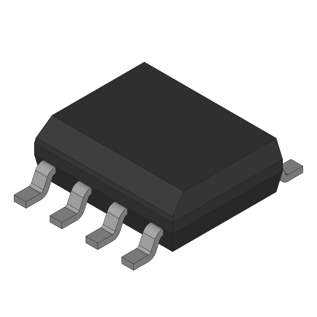
| 产品图片 |
|
| rohs | 符合RoHS无铅 / 符合限制有害物质指令(RoHS)规范要求 |
| 产品系列 | 逻辑集成电路,转换 - 电压电平,NXP Semiconductors GTL2002D,118- |
| 数据手册 | |
| 产品型号 | GTL2002D,118 |
| PCN封装 | |
| 产品培训模块 | http://www.digikey.cn/PTM/IndividualPTM.page?site=cn&lang=zhs&ptm=24983 |
| 产品目录页面 | |
| 产品种类 | 转换 - 电压电平 |
| 传播延迟(最大值) | 1.5ns |
| 位数 | 2 |
| 供应商器件封装 | 8-SO |
| 其它名称 | 568-5019-1 |
| 包装 | 剪切带 (CT) |
| 商标 | NXP Semiconductors |
| 安装类型 | 表面贴装 |
| 安装风格 | SMD/SMT |
| 封装 | Reel |
| 封装/外壳 | 8-SOIC(0.154",3.90mm 宽) |
| 封装/箱体 | SOT-96 |
| 工作温度 | -40°C ~ 85°C |
| 工厂包装数量 | 2500 |
| 差分-输入:输出 | 无/无 |
| 数据速率 | - |
| 最大工作温度 | + 85 C |
| 最小工作温度 | - 40 C |
| 标准包装 | 1 |
| 特色产品 | http://www.digikey.com/cn/zh/ph/NXP/I2C.html |
| 电压-电源 | 3 V ~ 3.6 V |
| 电源电压-最大 | 5.5 V |
| 电源电压-最小 | 0 V |
| 输入类型 | 电压 |
| 输出/通道数 | 1 |
| 输出类型 | 电压 |
| 通道数 | 2 |
| 逻辑功能 | 变换器,双向 |
| 零件号别名 | GTL2002D-T |


- 商务部:美国ITC正式对集成电路等产品启动337调查
- 曝三星4nm工艺存在良率问题 高通将骁龙8 Gen1或转产台积电
- 太阳诱电将投资9.5亿元在常州建新厂生产MLCC 预计2023年完工
- 英特尔发布欧洲新工厂建设计划 深化IDM 2.0 战略
- 台积电先进制程称霸业界 有大客户加持明年业绩稳了
- 达到5530亿美元!SIA预计今年全球半导体销售额将创下新高
- 英特尔拟将自动驾驶子公司Mobileye上市 估值或超500亿美元
- 三星加码芯片和SET,合并消费电子和移动部门,撤换高东真等 CEO
- 三星电子宣布重大人事变动 还合并消费电子和移动部门
- 海关总署:前11个月进口集成电路产品价值2.52万亿元 增长14.8%


PDF Datasheet 数据手册内容提取
GTL2002 2-bit bidirectional low voltage translator Rev. 8 — 19 August 2013 Product data sheet 1. General description The Gunning Transceiver Logic - Transceiver Voltage Clamps (GTL-TVC) provide high-speed voltage translation with low ON-state resistance and minimal propagation delay. The GTL2002 provides 2 NMOS pass transistors (Sn and Dn) with a common gate (GREF) and a reference transistor (SREF and DREF). The device allows bidirectional voltage translations between 1.0V and 5.0V without use of a direction pin. When the Sn or Dn port is LOW the clamp is in the ON-state and a low resistance connection exists between the Sn and Dn ports. Assuming the higher voltage is on the Dn port, when the Dn port is HIGH, the voltage on the Sn port is limited to the voltage set by the reference transistor (SREF). When the Sn port is HIGH, the Dn port is pulled to V by CC the pull-up resistors. This functionality allows a seamless translation between higher and lower voltages selected by the user, without the need for directional control. All transistors have the same electrical characteristics and there is minimal deviation from one output to another in voltage or propagation delay. This is a benefit over discrete transistor voltage translation solutions, since the fabrication of the transistors is symmetrical. Because all transistors in the device are identical, SREF and DREF can be located on any of the other two matched Sn/Dn transistors, allowing for easier board layout. The translator's transistors provide excellent ESD protection to lower voltage devices and at the same time protect less ESD-resistant devices. 2. Features and benefits 2-bit bidirectional low voltage translator Allows voltage level translation between 1.0V, 1.2V, 1.5V, 1.8V, 2.5V, 3.3V and 5V buses, which allows direct interface with GTL, GTL+, LVTTL/TTL and 5V CMOS levels Provides bidirectional voltage translation with no direction pin Low 6.5 ON-state resistance (R ) between input and output pins (Sn/Dn) on Supports hot insertion No power supply required; will not latch up 5V tolerant inputs Low standby current Flow-through pinout for ease of printed-circuit board trace routing ESD protection exceeds 2000V HBM per JESD22-A114 and 1000V CDM per JESD22-C101 Packages offered: SO8, TSSOP8 (MSOP8), VSSOP8, XQFN8
GTL2002 NXP Semiconductors 2-bit bidirectional low voltage translator 3. Applications Any application that requires bidirectional or unidirectional voltage level translation from any voltage between 1.0V and 5.0V to any voltage between 1.0V and 5.0V The open-drain construction with no direction pin is ideal for bidirectional low voltage (e.g., 1.0V, 1.2V, 1.5V, or 1.8V) processor I2C-bus port translation to the normal 3.3V or 5.0V I2C-bus signal levels or GTL/GTL+ translation to LVTTL/TTL signal levels. 4. Ordering information Table 1. Ordering info rmation Type number Topside Package marking Name Description Version GTL2002D GTL2002 SO8 plastic small outline package; 8leads; bodywidth3.9mm SOT96-1 GTL2002DP 2002 TSSOP8[1] plastic thin shrink small outline package; 8leads; SOT505-1 bodywidth3mm GTL2002DC 2002 VSSOP8 plastic very thin shrink small outline package; 8leads; SOT765-1 bodywidth2.3mm GTL2002GM G2X[2] XQFN8 plastic extremely thin quad flat package; noleads; SOT902-2 8terminals; body1.61.60.5mm [1] Also known as MSOP8. [2] ‘X’ will change based on date code. 4.1 Ordering options Table 2. Ordering opt ions Type number Orderable Package Packing method Minimum Temperature partnumber order quantity GTL2002D GTL2002D,112 SO8 Standard marking 2000 T =40Cto+85C amb *IC'stube-DSC bulk pack GTL2002D GTL2002D,118 SO8 Reel 13” Q1/T1 2500 T =40Cto+85C amb *Standardmark SMD GTL2002DP GTL2002DP,118 TSSOP8 Reel 13” Q1/T1 2500 T =40Cto+85C amb *Standardmark SMD GTL2002DC GTL2002DC,125 VSSOP8 Reel 7” Q3/T4 3000 T =40Cto+85C amb *Standardmark GTL2002GM GTL2002GM,125 XQFN8 Reel 7” Q3/T4 4000 T =40Cto+85C amb *Standardmark GTL2002 All information provided in this document is subject to legal disclaimers. © NXP B.V. 2013. All rights reserved. Product data sheet Rev. 8 — 19 August 2013 2 of 27
GTL2002 NXP Semiconductors 2-bit bidirectional low voltage translator 5. Functional diagram DREF GREF D1 D2 SREF S1 S2 002aac784 Fig 1. Functional diagram 6. Pinning information 6.1 Pinning GND 1 8 GREF GND 1 8 GREF SREF 2 7 DREF SREF 2 7 DREF GTL2002D GTL2002DP S1 3 6 D1 S1 3 6 D1 S2 4 5 D2 S2 4 5 D2 002aac777 002aac778 Fig 2. Pin configuration for SO8 Fig 3. Pin configuration for TSSOP8 (MSOP8) GTL2002GM terminal 1 F index area E R G GND 1 8 7 DREF SREF 2 6 D1 SREF 1 8 GREF S1 2 7 DREF S1 3 5 D2 GTL2002DC 4 S2 3 6 D1 GND 4 5 D2 S2 002aac780 002aac779 Transparent top view Fig 4. Pin configuration for VSSOP8 Fig 5. Pin configuration for XQFN8 GTL2002 All information provided in this document is subject to legal disclaimers. © NXP B.V. 2013. All rights reserved. Product data sheet Rev. 8 — 19 August 2013 3 of 27
GTL2002 NXP Semiconductors 2-bit bidirectional low voltage translator 6.2 Pin description Table 3. Pin description Symbol Pin Description SO8, TSSOP8, VSSOP8 XQFN8U GND 1 4 ground (0V) SREF 2 1 source of reference transistor S1 3 2 port S1 S2 4 3 port S2 D2 5 5 port D2 D1 6 6 port D1 DREF 7 7 drain of reference transistor GREF 8 8 gate of reference transistor 7. Functional description Refer to Figure 1 “Functional diagram”. 7.1 Function selection Table 4. Function selection, HIGH to LOW translation Assuming Dn is at the higher voltage level. H=HIGH voltage level; L=LOW voltage level; X=Don’t care. GREF[1] DREF SREF Input Dn Output Sn Transistor H H 0V X X off H H V [4] H V [2][4] on TT TT H H V [4] L L[3] on TT L L 0V V [4] X X off TT [1] GREF should be at least 1.5V higher than SREF for best translator operation. [2] Sn is not pulled up or pulled down. [3] Sn follows the Dn input LOW. [4] V is equal to the SREF voltage. TT T able 5. Function selection, LOW to HIGH translation Assuming Dn is at the higher voltage level. H=HIGH voltage level; L=LOW voltage level; X=Don’t care. GREF[1] DREF SREF Input Sn Output Dn Transistor H H 0V X X off H H V [4] V [4] H[2] nearly off TT TT H H V [4] L L[3] on TT L L 0V V [4] X X off TT [1] GREF should be at least 1.5V higher than SREF for best translator operation. [2] Dn is pulled up to V through an external resistor. CC [3] Dn follows the Sn input LOW. [4] V is equal to the SREF voltage. TT GTL2002 All information provided in this document is subject to legal disclaimers. © NXP B.V. 2013. All rights reserved. Product data sheet Rev. 8 — 19 August 2013 4 of 27
GTL2002 NXP Semiconductors 2-bit bidirectional low voltage translator 8. Application design-in information 8.1 Bidirectional translation For the bidirectional clamping configuration, higher voltage to lower voltage or lower voltage to higher voltage, the GREF input must be connected to DREF and both pins pulled to HIGH side V through a pull-up resistor (typically 200k). A filter capacitor on CC DREF is recommended. The processor output can be totem pole or open-drain (pull-up resistors may be required) and the chipset output can be totem pole or open-drain (pull-up resistors are required to pull the Dn outputs to V ). However, if either output is CC totem pole, data must be unidirectional or the outputs must be 3-stateable and the outputs must be controlled by some direction control mechanism to prevent HIGH-to-LOW contentions in either direction. If both outputs are open-drain, no direction control is needed. The opposite side of the reference transistor (SREF) is connected to the processor core power supply voltage. When DREF is connected through a 200k resistor to a 3.3V to 5.5V V supply and SREF is set between 1.0V to (V 1.5V), CC CC the output of each Sn has a maximum output voltage equal to SREF and the output of each Dn has a maximum output voltage equal to V . CC 1.8 V 5 V 1.5 V 1.2 V 200 kΩ totem pole or 1.0 V open-drain I/O GND GREF VCORE SREF DREF VCC S1 D1 CPU I/O CHIPSET I/O S2 D2 increase bit size 3.3 V by using 10-bit GTL2010 or 22-bit GTL2000 VCC S3 D3 CHIPSET I/O S4 D4 S5 D5 Sn Dn 002aac060 Typical bidirectional voltage translation. Fig 6. Bidirectional translation to multiple higher voltage levels such as an I2C-bus application GTL2002 All information provided in this document is subject to legal disclaimers. © NXP B.V. 2013. All rights reserved. Product data sheet Rev. 8 — 19 August 2013 5 of 27
GTL2002 NXP Semiconductors 2-bit bidirectional low voltage translator 8.2 Unidirectional down translation For unidirectional clamping, higher voltage to lower voltage, the GREF input must be connected to DREF and both pins pulled to the higher side V through a pull-up resistor CC (typically 200k). A filter capacitor on DREF is recommended. Pull-up resistors are required if the chipset I/O are open-drain. The opposite side of the reference transistor (SREF) is connected to the processor core supply voltage. When DREF is connected through a 200k resistor to a 3.3V to 5.5V V supply and SREF is set between 1.0V CC to (V 1.5V), the output of each Sn has a maximum output voltage equal to SREF. CC 1.8 V 5 V 1.5 V 1.2 V 200 kΩ 1.0 V 0.8 V GTL2003 easy migration to lower voltage as processor geometry shrinks GND GREF VCORE SREF DREF VDD1 S1 D1 CPU I/O CHIPSET I/O S2 D2 totem pole I/O S8 D8 002aac061 Typical unidirectional HIGH-to-LOW voltage translation. Fig 7. Unidirectional down translation to protect low voltage processor pins 8.3 Unidirectional up translation For unidirectional up translation, lower voltage to higher voltage, the reference transistor is connected the same as for a down translation. A pull-up resistor is required on the higher voltage side (Dn or Sn) to get the full HIGH level, since the GTL-TVC device will only pass the reference source (SREF) voltage as a HIGH when doing an up translation. The driver on the lower voltage side only needs pull-up resistors if it is open-drain. 1.8 V 5 V 1.5 V 1.2 V 200 kΩ 1.0 V 0.8 V GTL2003 easy migration to lower voltage as processor geometry shrinks GND GREF VCORE SREF DREF VDD1 SS11 DD11 CPU I/O CHIPSET I/O S2 D2 totem pole I/O or open-drain S8 D8 002aac062 Typical unidirectional LOW-to-HIGH voltage translation. Fig 8. Unidirectional up translation to higher voltage chip sets GTL2002 All information provided in this document is subject to legal disclaimers. © NXP B.V. 2013. All rights reserved. Product data sheet Rev. 8 — 19 August 2013 6 of 27
GTL2002 NXP Semiconductors 2-bit bidirectional low voltage translator 8.4 Sizing pull-up resistor The pull-up resistor value needs to limit the current through the pass transistor when it is in the ON state to about 15mA. This will guarantee a pass voltage of 260mV to 350mV. If the current through the pass transistor is higher than 15mA, the pass voltage will also be higher in the ON state. To set the current through each pass transistor at 15mA, the pull-up resistor value is calculated as shown in Equation1: pull-up voltage V–0.35 V resistor value = -------------------------------------------------------------------------- (1) 0.015 A Table6 summarizes resistor values for various reference voltages and currents at 15mA and also at 10mA and 3mA. The resistor value shown in the +10% column or a larger value should be used to ensure that the pass voltage of the transistor would be 350mV or less. The external driver must be able to sink the total current from the resistors on both sides of the GTL-TVC device at 0.175V, although the 15mA only applies to current flowing through the GTL-TVC device. See application note AN10145, “Bidirectional low voltage translators” for more information. Table 6. Pull-up resistor values Pull-up resistor value ()[1] Voltage 15mA[2] 10mA[2] 3mA[2] Nominal +10%[3] Nominal +10%[3] Nominal +10%[3] 5.0V 310 341 465 512 1550 1705 3.3V 197 217 295 325 983 1082 2.5V 143 158 215 237 717 788 1.8V 97 106 145 160 483 532 1.5V 77 85 115 127 383 422 1.2V 57 63 85 94 283 312 [1] Calculated for V =0.35V. OL [2] Assumes output driver V =0.175 V at stated current. OL [3] +10% to compensate for V range and resistor tolerance. DD GTL2002 All information provided in this document is subject to legal disclaimers. © NXP B.V. 2013. All rights reserved. Product data sheet Rev. 8 — 19 August 2013 7 of 27
GTL2002 NXP Semiconductors 2-bit bidirectional low voltage translator 9. Limiting values Table 7. Limiting values[1] In accordance with the Absolute Maximum Rating System (IEC 60134). Symbol Parameter Conditions Min Max Unit V voltage on pin SREF [2] 0.5 +7.0 V SREF V voltage on pin DREF [2] 0.5 +7.0 V DREF V voltage on pin GREF [2] 0.5 +7.0 V GREF V voltage on port Sn [2] 0.5 +7.0 V Sn V voltage on port Dn [2] 0.5 +7.0 V Dn I diode current on reference pins V <0V - 50 mA REFK I I diode current port Sn V <0V - 50 mA SK I I diode current port Dn V <0V - 50 mA DK I I clamp current per channel channel in ON state - 128 mA max T storage temperature 65 +150 C stg [1] The performance capability of a high-performance integrated circuit in conjunction with its thermal environment can create junction temperature which are detrimental to reliability. The maximum junction temperature of this integrated circuit should not exceed 150C. [2] The input and output negative voltage ratings may be exceeded if the input and output clamp current ratings are observed. 10. Recommended operating conditions Table 8. Recommended operating conditions Symbol Parameter Conditions Min Max Unit V voltage on an input/outputpin Sn, Dn 0 5.5 V I/O V voltage on pin SREF [1] 0 5.5 V SREF V voltage on pin DREF 0 5.5 V DREF V voltage on pin GREF 0 5.5 V GREF I pass transistor current - 64 mA PASS T ambient temperature operating in freeair 40 +85 C amb [1] VSREFVDREF1.5V for best results in level shifting applications. GTL2002 All information provided in this document is subject to legal disclaimers. © NXP B.V. 2013. All rights reserved. Product data sheet Rev. 8 — 19 August 2013 8 of 27
GTL2002 NXP Semiconductors 2-bit bidirectional low voltage translator 11. Static characteristics Table 9. Static charac teristics T =40C to +85C, unless otherwise specified. amb Symbol Parameter Conditions Min Typ[1] Max Unit V LOW-level output voltage V =3.0V; V =1.365V; - 260 350 mV OL DD SREF V orV =0.175V; Sn Dn I =15.2mA clamp V input clamping voltage I =18mA; V =0V - - 1.2 V IK I GREF I gate input leakage current V =5V; V =0V - - 5 A LI(gate) I GREF C input capacitance at gate pin GREF; V =3V or 0V - 19.4 - pF ig I C off-state input/output capacitance V =3V or 0V; V =0V [2] - 7.4 - pF io(off) O GREF C on-state input/output capacitance V =3V or 0V; V =3V [2] - 18.6 - pF io(on) O GREF R ON-state resistance V =0V; I =64mA [3] on I O V =4.5V - 3.5 5 GREF V =3V - 4.4 7 GREF V =2.3V - 5.5 9 GREF V =1.5V - 67 105 GREF V =0V; I =30mA; [3] - 9 15 I O V =1.5V GREF V =2.4V; I =15mA; [3] - 7 10 I O V =4.5V GREF V =2.4V; I =15mA; [3] - 58 80 I O V =3V GREF V =1.7V; I =15mA; [3] - 50 70 I O V =2.3V GREF [1] All typical values are measured at Tamb=25C. [2] C maximum of 30pF and C maximum of 15pF is guaranteed by design. io(on) io(off) [3] Measured by the voltage drop between the Sn and the Dn terminals at the indicated current through the switch. ON-state resistance is determined by the lowest voltage of the two (Sn or Dn) terminals. GTL2002 All information provided in this document is subject to legal disclaimers. © NXP B.V. 2013. All rights reserved. Product data sheet Rev. 8 — 19 August 2013 9 of 27
GTL2002 NXP Semiconductors 2-bit bidirectional low voltage translator 12. Dynamic characteristics 12.1 Dynamic characteristics for translator-type application Table 10. Dynamic characteristics for translator-type application T = 40C to +85C; V =1.365V to 1.635V; V =3.0V to 3.6V; V = 2.36V to 2.64V; amb ref DD1 DD2 GND=0V; t =t 3.0ns. Refer to Figure11. r f Symbol Parameter Conditions Min Typ[1] Max Unit t LOWtoHIGH Sn to Dn; Dn to Sn [2] 0.5 1.5 5.5 ns PLH propagation delay t HIGHtoLOW Sn to Dn; Dn to Sn [2] 0.5 1.5 5.5 ns PHL propagation delay [1] All typical values are measured at VDD1=3.3V, VDD2=2.5V; Vref=1.5V and Tamb=25C. [2] Propagation delay guaranteed by characterization. VI input VM VM GND tPHL0 tPLH0 test jig output VDD2 HIGH-to-LOW, VM VM LOW-to-HIGH VOL tPHL tPLH tPHL1 tPLH1 DUT output VDD2 HIGH-to-LOW, VM VM LOW-to-HIGH VOL 002aac789 V =1.5V; V =GND to 3.0V. M I Fig 9. The input (Sn) to output (Dn) propagation delays GTL2002 All information provided in this document is subject to legal disclaimers. © NXP B.V. 2013. All rights reserved. Product data sheet Rev. 8 — 19 August 2013 10 of 27
GTL2002 NXP Semiconductors 2-bit bidirectional low voltage translator 12.2 Dynamic characteristics for CBT-type application Table 11. Dynamic characteristics for CBT-type application T = 40C to +85C; V =5V0.5V; GND=0V; t =t 3.0ns; C =50pF. amb GREF r f L Symbol Parameter Conditions Min Typ Max Unit t propagation delay [1] - - 250 ps PD [1] This parameter is warranted by the ON-state resistance at GREF=4.5V, but is not directly production tested. The propagation delay is based on the RC time constant of the typical ON-state resistance of the switch and a load capacitance of 50pF, when driven by an ideal voltage source (zero output impedance). 3.0 V input 1.5 V 1.5 V 0 V tPLH tPHL VOH output 1.5 V 1.5 V VOL 002aab664 t = the maximum of t or t . PD PLH PHL V =1.5V; V =GND to 3.0V. M I Fig 10. Input (Sn) to output (Dn) propagation delays GTL2002 All information provided in this document is subject to legal disclaimers. © NXP B.V. 2013. All rights reserved. Product data sheet Rev. 8 — 19 August 2013 11 of 27
GTL2002 NXP Semiconductors 2-bit bidirectional low voltage translator 13. Test information VDD1 VDD2 VDD2 VDD2 200 kΩ 150 kΩ 150 kΩ 150 kΩ DREF GREF D1 D2 DUT SREF S1 S2 test jig Vref pulse generator 002aac790 Fig 11. Load circuit for translator-type applications RL S1 7 V from output under test open 500 Ω GND CL RL 50 pF 500 Ω 002aab667 Test data are given in Table12. C =load capacitance; includes jig and probe capacitance. L RL=load resistance. Fig 12. Load circuit for CBT-type application T able 12. Test data Test Load Switch C R L L t 50pF 500 open PD GTL2002 All information provided in this document is subject to legal disclaimers. © NXP B.V. 2013. All rights reserved. Product data sheet Rev. 8 — 19 August 2013 12 of 27
GTL2002 NXP Semiconductors 2-bit bidirectional low voltage translator 14. Package outline (cid:54)(cid:50)(cid:27)(cid:29)(cid:3)(cid:83)(cid:79)(cid:68)(cid:86)(cid:87)(cid:76)(cid:70)(cid:3)(cid:86)(cid:80)(cid:68)(cid:79)(cid:79)(cid:3)(cid:82)(cid:88)(cid:87)(cid:79)(cid:76)(cid:81)(cid:72)(cid:3)(cid:83)(cid:68)(cid:70)(cid:78)(cid:68)(cid:74)(cid:72)(cid:30)(cid:3)(cid:27)(cid:3)(cid:79)(cid:72)(cid:68)(cid:71)(cid:86)(cid:30)(cid:3)(cid:69)(cid:82)(cid:71)(cid:92)(cid:3)(cid:90)(cid:76)(cid:71)(cid:87)(cid:75)(cid:3)(cid:22)(cid:17)(cid:28)(cid:3)(cid:80)(cid:80)(cid:3) (cid:54)(cid:50)(cid:55)(cid:28)(cid:25)(cid:16)(cid:20)(cid:3) (cid:39)(cid:3) (cid:40)(cid:3) (cid:36)(cid:3) (cid:59)(cid:3) (cid:70)(cid:3) (cid:92)(cid:3) (cid:43)(cid:3)(cid:40)(cid:3) (cid:89)(cid:3)(cid:48)(cid:3) (cid:36)(cid:3) (cid:61)(cid:3) (cid:27)(cid:3) (cid:24)(cid:3) (cid:52)(cid:3) (cid:36)(cid:3)(cid:21)(cid:3)(cid:36)(cid:3)(cid:20)(cid:3) (cid:11)(cid:36)(cid:3)(cid:22)(cid:3)(cid:3)(cid:12)(cid:3) (cid:36)(cid:3) (cid:83)(cid:76)(cid:81)(cid:3)(cid:20)(cid:3)(cid:76)(cid:81)(cid:71)(cid:72)(cid:91)(cid:3) (cid:537)(cid:3) (cid:47)(cid:3)(cid:83)(cid:3) (cid:20)(cid:3) (cid:23)(cid:3) (cid:47)(cid:3) (cid:72)(cid:3) (cid:90)(cid:3)(cid:48)(cid:3) (cid:71)(cid:72)(cid:87)(cid:68)(cid:76)(cid:79)(cid:3)(cid:59)(cid:3) (cid:69)(cid:3)(cid:83)(cid:3) (cid:19)(cid:3) (cid:21)(cid:17)(cid:24)(cid:3) (cid:24)(cid:3)(cid:80)(cid:80)(cid:3) (cid:86)(cid:70)(cid:68)(cid:79)(cid:72)(cid:3) (cid:39)(cid:44)(cid:48)(cid:40)(cid:49)(cid:54)(cid:44)(cid:50)(cid:49)(cid:54)(cid:3)(cid:11)(cid:76)(cid:81)(cid:70)(cid:75)(cid:3)(cid:71)(cid:76)(cid:80)(cid:72)(cid:81)(cid:86)(cid:76)(cid:82)(cid:81)(cid:86)(cid:3)(cid:68)(cid:85)(cid:72)(cid:3)(cid:71)(cid:72)(cid:85)(cid:76)(cid:89)(cid:72)(cid:71)(cid:3)(cid:73)(cid:85)(cid:82)(cid:80)(cid:3)(cid:87)(cid:75)(cid:72)(cid:3)(cid:82)(cid:85)(cid:76)(cid:74)(cid:76)(cid:81)(cid:68)(cid:79)(cid:3)(cid:80)(cid:80)(cid:3)(cid:71)(cid:76)(cid:80)(cid:72)(cid:81)(cid:86)(cid:76)(cid:82)(cid:81)(cid:86)(cid:12)(cid:3) (cid:56)(cid:49)(cid:44)(cid:55)(cid:3) (cid:80)(cid:36)(cid:68)(cid:91)(cid:3)(cid:17)(cid:3) (cid:36)(cid:3)(cid:20)(cid:3) (cid:36)(cid:3)(cid:21)(cid:3) (cid:36)(cid:3)(cid:22)(cid:3) (cid:69)(cid:3)(cid:83)(cid:3) (cid:70)(cid:3) (cid:39)(cid:3)(cid:11)(cid:20)(cid:12)(cid:3) (cid:40)(cid:3)(cid:11)(cid:21)(cid:12)(cid:3) (cid:72)(cid:3) (cid:43)(cid:3)(cid:40)(cid:3) (cid:47)(cid:3) (cid:47)(cid:3)(cid:83)(cid:3) (cid:52)(cid:3) (cid:89)(cid:3) (cid:90)(cid:3) (cid:92)(cid:3) (cid:61)(cid:3)(cid:11)(cid:20)(cid:12)(cid:3) (cid:537)(cid:3) (cid:19)(cid:17)(cid:21)(cid:24)(cid:3) (cid:20)(cid:17)(cid:23)(cid:24)(cid:3) (cid:19)(cid:17)(cid:23)(cid:28)(cid:3) (cid:19)(cid:17)(cid:21)(cid:24)(cid:3) (cid:24)(cid:17)(cid:19)(cid:3) (cid:23)(cid:17)(cid:19)(cid:3) (cid:25)(cid:17)(cid:21)(cid:3) (cid:20)(cid:17)(cid:19)(cid:3) (cid:19)(cid:17)(cid:26)(cid:3) (cid:19)(cid:17)(cid:26)(cid:3) (cid:80)(cid:80)(cid:3) (cid:20)(cid:17)(cid:26)(cid:24)(cid:3) (cid:19)(cid:17)(cid:21)(cid:24)(cid:3) (cid:20)(cid:17)(cid:21)(cid:26)(cid:3) (cid:20)(cid:17)(cid:19)(cid:24)(cid:3) (cid:19)(cid:17)(cid:21)(cid:24)(cid:3) (cid:19)(cid:17)(cid:21)(cid:24)(cid:3) (cid:19)(cid:17)(cid:20)(cid:3) (cid:19)(cid:17)(cid:20)(cid:19)(cid:3) (cid:20)(cid:17)(cid:21)(cid:24)(cid:3) (cid:19)(cid:17)(cid:22)(cid:25)(cid:3) (cid:19)(cid:17)(cid:20)(cid:28)(cid:3) (cid:23)(cid:17)(cid:27)(cid:3) (cid:22)(cid:17)(cid:27)(cid:3) (cid:24)(cid:17)(cid:27)(cid:3) (cid:19)(cid:17)(cid:23)(cid:3) (cid:19)(cid:17)(cid:25)(cid:3) (cid:19)(cid:17)(cid:22)(cid:3) (cid:27)(cid:3)(cid:82)(cid:3) (cid:19)(cid:17)(cid:19)(cid:20)(cid:19)(cid:3) (cid:19)(cid:17)(cid:19)(cid:24)(cid:26)(cid:3) (cid:19)(cid:17)(cid:19)(cid:20)(cid:28)(cid:3)(cid:19)(cid:17)(cid:19)(cid:20)(cid:19)(cid:19)(cid:3) (cid:19)(cid:17)(cid:21)(cid:19)(cid:3) (cid:19)(cid:17)(cid:20)(cid:25)(cid:3) (cid:19)(cid:17)(cid:21)(cid:23)(cid:23)(cid:3) (cid:19)(cid:17)(cid:19)(cid:22)(cid:28)(cid:3) (cid:19)(cid:17)(cid:19)(cid:21)(cid:27)(cid:3) (cid:19)(cid:17)(cid:19)(cid:21)(cid:27)(cid:3) (cid:19)(cid:3)(cid:82)(cid:3) (cid:76)(cid:81)(cid:70)(cid:75)(cid:72)(cid:86)(cid:3) (cid:19)(cid:17)(cid:19)(cid:25)(cid:28)(cid:3) (cid:19)(cid:17)(cid:19)(cid:20)(cid:3) (cid:19)(cid:17)(cid:19)(cid:24)(cid:3) (cid:19)(cid:17)(cid:19)(cid:23)(cid:20)(cid:3) (cid:19)(cid:17)(cid:19)(cid:20)(cid:3) (cid:19)(cid:17)(cid:19)(cid:20)(cid:3) (cid:19)(cid:17)(cid:19)(cid:19)(cid:23)(cid:3) (cid:19)(cid:17)(cid:19)(cid:19)(cid:23)(cid:3) (cid:19)(cid:17)(cid:19)(cid:23)(cid:28)(cid:3) (cid:19)(cid:17)(cid:19)(cid:20)(cid:23)(cid:3)(cid:19)(cid:17)(cid:19)(cid:19)(cid:26)(cid:24)(cid:3) (cid:19)(cid:17)(cid:20)(cid:28)(cid:3) (cid:19)(cid:17)(cid:20)(cid:24)(cid:3) (cid:19)(cid:17)(cid:21)(cid:21)(cid:27)(cid:3) (cid:19)(cid:17)(cid:19)(cid:20)(cid:25)(cid:3) (cid:19)(cid:17)(cid:19)(cid:21)(cid:23)(cid:3) (cid:19)(cid:17)(cid:19)(cid:20)(cid:21)(cid:3) (cid:49)(cid:82)(cid:87)(cid:72)(cid:86)(cid:3) (cid:20)(cid:17)(cid:3)(cid:51)(cid:79)(cid:68)(cid:86)(cid:87)(cid:76)(cid:70)(cid:3)(cid:82)(cid:85)(cid:3)(cid:80)(cid:72)(cid:87)(cid:68)(cid:79)(cid:3)(cid:83)(cid:85)(cid:82)(cid:87)(cid:85)(cid:88)(cid:86)(cid:76)(cid:82)(cid:81)(cid:86)(cid:3)(cid:82)(cid:73)(cid:3)(cid:19)(cid:17)(cid:20)(cid:24)(cid:3)(cid:80)(cid:80)(cid:3)(cid:11)(cid:19)(cid:17)(cid:19)(cid:19)(cid:25)(cid:3)(cid:76)(cid:81)(cid:70)(cid:75)(cid:12)(cid:3)(cid:80)(cid:68)(cid:91)(cid:76)(cid:80)(cid:88)(cid:80)(cid:3)(cid:83)(cid:72)(cid:85)(cid:3)(cid:86)(cid:76)(cid:71)(cid:72)(cid:3)(cid:68)(cid:85)(cid:72)(cid:3)(cid:81)(cid:82)(cid:87)(cid:3)(cid:76)(cid:81)(cid:70)(cid:79)(cid:88)(cid:71)(cid:72)(cid:71)(cid:17)(cid:3) (cid:21)(cid:17)(cid:3)(cid:51)(cid:79)(cid:68)(cid:86)(cid:87)(cid:76)(cid:70)(cid:3)(cid:82)(cid:85)(cid:3)(cid:80)(cid:72)(cid:87)(cid:68)(cid:79)(cid:3)(cid:83)(cid:85)(cid:82)(cid:87)(cid:85)(cid:88)(cid:86)(cid:76)(cid:82)(cid:81)(cid:86)(cid:3)(cid:82)(cid:73)(cid:3)(cid:19)(cid:17)(cid:21)(cid:24)(cid:3)(cid:80)(cid:80)(cid:3)(cid:11)(cid:19)(cid:17)(cid:19)(cid:20)(cid:3)(cid:76)(cid:81)(cid:70)(cid:75)(cid:12)(cid:3)(cid:80)(cid:68)(cid:91)(cid:76)(cid:80)(cid:88)(cid:80)(cid:3)(cid:83)(cid:72)(cid:85)(cid:3)(cid:86)(cid:76)(cid:71)(cid:72)(cid:3)(cid:68)(cid:85)(cid:72)(cid:3)(cid:81)(cid:82)(cid:87)(cid:3)(cid:76)(cid:81)(cid:70)(cid:79)(cid:88)(cid:71)(cid:72)(cid:71)(cid:17)(cid:3)(cid:3) (cid:50)(cid:56)(cid:55)(cid:47)(cid:44)(cid:49)(cid:40)(cid:3) (cid:3)(cid:53)(cid:40)(cid:41)(cid:40)(cid:53)(cid:40)(cid:49)(cid:38)(cid:40)(cid:54)(cid:3) (cid:40)(cid:56)(cid:53)(cid:50)(cid:51)(cid:40)(cid:36)(cid:49)(cid:3) (cid:44)(cid:54)(cid:54)(cid:56)(cid:40)(cid:3)(cid:39)(cid:36)(cid:55)(cid:40)(cid:3) (cid:57)(cid:40)(cid:53)(cid:54)(cid:44)(cid:50)(cid:49)(cid:3) (cid:3)(cid:44)(cid:40)(cid:38)(cid:3) (cid:3)(cid:45)(cid:40)(cid:39)(cid:40)(cid:38)(cid:3) (cid:3)(cid:45)(cid:40)(cid:44)(cid:55)(cid:36)(cid:3) (cid:51)(cid:53)(cid:50)(cid:45)(cid:40)(cid:38)(cid:55)(cid:44)(cid:50)(cid:49)(cid:3) (cid:28)(cid:28)(cid:16)(cid:20)(cid:21)(cid:16)(cid:21)(cid:26)(cid:3) (cid:3)(cid:54)(cid:50)(cid:55)(cid:28)(cid:25)(cid:16)(cid:20)(cid:3) (cid:19)(cid:26)(cid:25)(cid:40)(cid:19)(cid:22)(cid:3) (cid:3)(cid:48)(cid:54)(cid:16)(cid:19)(cid:20)(cid:21)(cid:3) (cid:19)(cid:22)(cid:16)(cid:19)(cid:21)(cid:16)(cid:20)(cid:27)(cid:3) Fig 13. Package outline SOT96-1 (SO8) GTL2002 All information provided in this document is subject to legal disclaimers. © NXP B.V. 2013. All rights reserved. Product data sheet Rev. 8 — 19 August 2013 13 of 27
GTL2002 NXP Semiconductors 2-bit bidirectional low voltage translator (cid:55)(cid:54)(cid:54)(cid:50)(cid:51)(cid:27)(cid:29)(cid:3)(cid:83)(cid:79)(cid:68)(cid:86)(cid:87)(cid:76)(cid:70)(cid:3)(cid:87)(cid:75)(cid:76)(cid:81)(cid:3)(cid:86)(cid:75)(cid:85)(cid:76)(cid:81)(cid:78)(cid:3)(cid:86)(cid:80)(cid:68)(cid:79)(cid:79)(cid:3)(cid:82)(cid:88)(cid:87)(cid:79)(cid:76)(cid:81)(cid:72)(cid:3)(cid:83)(cid:68)(cid:70)(cid:78)(cid:68)(cid:74)(cid:72)(cid:30)(cid:3)(cid:27)(cid:3)(cid:79)(cid:72)(cid:68)(cid:71)(cid:86)(cid:30)(cid:3)(cid:69)(cid:82)(cid:71)(cid:92)(cid:3)(cid:90)(cid:76)(cid:71)(cid:87)(cid:75)(cid:3)(cid:22)(cid:3)(cid:80)(cid:80)(cid:3) (cid:54)(cid:50)(cid:55)(cid:24)(cid:19)(cid:24)(cid:16)(cid:20)(cid:3) (cid:39)(cid:3) (cid:40)(cid:3) (cid:36)(cid:3) (cid:59)(cid:3) (cid:70)(cid:3) (cid:92)(cid:3) (cid:43)(cid:40)(cid:3) (cid:89)(cid:3)(cid:48)(cid:3) (cid:36)(cid:3) (cid:61)(cid:3) (cid:27)(cid:3) (cid:24)(cid:3) (cid:36)(cid:21)(cid:3)(cid:36)(cid:20)(cid:3) (cid:11)(cid:36)(cid:22)(cid:12)(cid:3) (cid:36)(cid:3) (cid:83)(cid:76)(cid:81)(cid:3)(cid:20)(cid:3)(cid:76)(cid:81)(cid:71)(cid:72)(cid:91)(cid:3) (cid:537)(cid:3) (cid:47)(cid:83)(cid:3) (cid:47)(cid:3) (cid:20)(cid:3) (cid:23)(cid:3) (cid:71)(cid:72)(cid:87)(cid:68)(cid:76)(cid:79)(cid:3)(cid:59)(cid:3) (cid:72)(cid:3) (cid:90)(cid:3)(cid:48)(cid:3) (cid:69)(cid:83)(cid:3) (cid:19)(cid:3) (cid:21)(cid:17)(cid:24)(cid:3) (cid:24)(cid:3)(cid:80)(cid:80)(cid:3) (cid:86)(cid:70)(cid:68)(cid:79)(cid:72)(cid:3) (cid:39)(cid:44)(cid:48)(cid:40)(cid:49)(cid:54)(cid:44)(cid:50)(cid:49)(cid:54)(cid:3)(cid:11)(cid:80)(cid:80)(cid:3)(cid:68)(cid:85)(cid:72)(cid:3)(cid:87)(cid:75)(cid:72)(cid:3)(cid:82)(cid:85)(cid:76)(cid:74)(cid:76)(cid:81)(cid:68)(cid:79)(cid:3)(cid:71)(cid:76)(cid:80)(cid:72)(cid:81)(cid:86)(cid:76)(cid:82)(cid:81)(cid:86)(cid:12)(cid:3) (cid:56)(cid:49)(cid:44)(cid:55)(cid:3) (cid:80)(cid:36)(cid:68)(cid:91)(cid:3)(cid:17)(cid:3) (cid:36)(cid:20)(cid:3) (cid:36)(cid:21)(cid:3) (cid:36)(cid:22)(cid:3) (cid:69)(cid:83)(cid:3) (cid:70)(cid:3) (cid:39)(cid:11)(cid:20)(cid:12)(cid:3) (cid:40)(cid:11)(cid:21)(cid:12)(cid:3) (cid:72)(cid:3) (cid:43)(cid:40)(cid:3) (cid:47)(cid:3) (cid:47)(cid:83)(cid:3) (cid:89)(cid:3) (cid:90)(cid:3) (cid:92)(cid:3) (cid:61)(cid:11)(cid:20)(cid:12)(cid:3) (cid:537)(cid:3) (cid:19)(cid:17)(cid:20)(cid:24)(cid:3) (cid:19)(cid:17)(cid:28)(cid:24)(cid:3) (cid:19)(cid:17)(cid:23)(cid:24)(cid:3) (cid:19)(cid:17)(cid:21)(cid:27)(cid:3) (cid:22)(cid:17)(cid:20)(cid:3) (cid:22)(cid:17)(cid:20)(cid:3) (cid:24)(cid:17)(cid:20)(cid:3) (cid:19)(cid:17)(cid:26)(cid:3) (cid:19)(cid:17)(cid:26)(cid:19)(cid:3) (cid:25)(cid:131)(cid:3) (cid:80)(cid:80)(cid:3) (cid:20)(cid:17)(cid:20)(cid:3) (cid:19)(cid:17)(cid:21)(cid:24)(cid:3) (cid:19)(cid:17)(cid:25)(cid:24)(cid:3) (cid:19)(cid:17)(cid:28)(cid:23)(cid:3) (cid:19)(cid:17)(cid:20)(cid:3) (cid:19)(cid:17)(cid:20)(cid:3) (cid:19)(cid:17)(cid:20)(cid:3) (cid:19)(cid:17)(cid:19)(cid:24)(cid:3) (cid:19)(cid:17)(cid:27)(cid:19)(cid:3) (cid:19)(cid:17)(cid:21)(cid:24)(cid:3) (cid:19)(cid:17)(cid:20)(cid:24)(cid:3) (cid:21)(cid:17)(cid:28)(cid:3) (cid:21)(cid:17)(cid:28)(cid:3) (cid:23)(cid:17)(cid:26)(cid:3) (cid:19)(cid:17)(cid:23)(cid:3) (cid:19)(cid:17)(cid:22)(cid:24)(cid:3) (cid:19)(cid:131)(cid:3) (cid:49)(cid:82)(cid:87)(cid:72)(cid:86)(cid:3) (cid:20)(cid:17)(cid:3)(cid:51)(cid:79)(cid:68)(cid:86)(cid:87)(cid:76)(cid:70)(cid:3)(cid:82)(cid:85)(cid:3)(cid:80)(cid:72)(cid:87)(cid:68)(cid:79)(cid:3)(cid:83)(cid:85)(cid:82)(cid:87)(cid:85)(cid:88)(cid:86)(cid:76)(cid:82)(cid:81)(cid:86)(cid:3)(cid:82)(cid:73)(cid:3)(cid:19)(cid:17)(cid:20)(cid:24)(cid:3)(cid:80)(cid:80)(cid:3)(cid:80)(cid:68)(cid:91)(cid:76)(cid:80)(cid:88)(cid:80)(cid:3)(cid:83)(cid:72)(cid:85)(cid:3)(cid:86)(cid:76)(cid:71)(cid:72)(cid:3)(cid:68)(cid:85)(cid:72)(cid:3)(cid:81)(cid:82)(cid:87)(cid:3)(cid:76)(cid:81)(cid:70)(cid:79)(cid:88)(cid:71)(cid:72)(cid:71)(cid:17)(cid:3) (cid:21)(cid:17)(cid:3)(cid:51)(cid:79)(cid:68)(cid:86)(cid:87)(cid:76)(cid:70)(cid:3)(cid:82)(cid:85)(cid:3)(cid:80)(cid:72)(cid:87)(cid:68)(cid:79)(cid:3)(cid:83)(cid:85)(cid:82)(cid:87)(cid:85)(cid:88)(cid:86)(cid:76)(cid:82)(cid:81)(cid:86)(cid:3)(cid:82)(cid:73)(cid:3)(cid:19)(cid:17)(cid:21)(cid:24)(cid:3)(cid:80)(cid:80)(cid:3)(cid:80)(cid:68)(cid:91)(cid:76)(cid:80)(cid:88)(cid:80)(cid:3)(cid:83)(cid:72)(cid:85)(cid:3)(cid:86)(cid:76)(cid:71)(cid:72)(cid:3)(cid:68)(cid:85)(cid:72)(cid:3)(cid:81)(cid:82)(cid:87)(cid:3)(cid:76)(cid:81)(cid:70)(cid:79)(cid:88)(cid:71)(cid:72)(cid:71)(cid:17)(cid:3) (cid:50)(cid:56)(cid:55)(cid:47)(cid:44)(cid:49)(cid:40)(cid:3) (cid:3)(cid:53)(cid:40)(cid:41)(cid:40)(cid:53)(cid:40)(cid:49)(cid:38)(cid:40)(cid:54)(cid:3) (cid:40)(cid:56)(cid:53)(cid:50)(cid:51)(cid:40)(cid:36)(cid:49)(cid:3) (cid:44)(cid:54)(cid:54)(cid:56)(cid:40)(cid:3)(cid:39)(cid:36)(cid:55)(cid:40)(cid:3) (cid:57)(cid:40)(cid:53)(cid:54)(cid:44)(cid:50)(cid:49)(cid:3) (cid:3)(cid:44)(cid:40)(cid:38)(cid:3) (cid:3)(cid:45)(cid:40)(cid:39)(cid:40)(cid:38)(cid:3) (cid:3)(cid:45)(cid:40)(cid:44)(cid:55)(cid:36)(cid:3) (cid:51)(cid:53)(cid:50)(cid:45)(cid:40)(cid:38)(cid:55)(cid:44)(cid:50)(cid:49)(cid:3) (cid:28)(cid:28)(cid:16)(cid:19)(cid:23)(cid:16)(cid:19)(cid:28)(cid:3) (cid:3)(cid:54)(cid:50)(cid:55)(cid:24)(cid:19)(cid:24)(cid:16)(cid:20)(cid:3) (cid:3) (cid:19)(cid:22)(cid:16)(cid:19)(cid:21)(cid:16)(cid:20)(cid:27)(cid:3) Fig 14. Package outline SOT505-1 (TSSOP8) GTL2002 All information provided in this document is subject to legal disclaimers. © NXP B.V. 2013. All rights reserved. Product data sheet Rev. 8 — 19 August 2013 14 of 27
GTL2002 NXP Semiconductors 2-bit bidirectional low voltage translator (cid:57)(cid:54)(cid:54)(cid:50)(cid:51)(cid:27)(cid:29)(cid:3)(cid:83)(cid:79)(cid:68)(cid:86)(cid:87)(cid:76)(cid:70)(cid:3)(cid:89)(cid:72)(cid:85)(cid:92)(cid:3)(cid:87)(cid:75)(cid:76)(cid:81)(cid:3)(cid:86)(cid:75)(cid:85)(cid:76)(cid:81)(cid:78)(cid:3)(cid:86)(cid:80)(cid:68)(cid:79)(cid:79)(cid:3)(cid:82)(cid:88)(cid:87)(cid:79)(cid:76)(cid:81)(cid:72)(cid:3)(cid:83)(cid:68)(cid:70)(cid:78)(cid:68)(cid:74)(cid:72)(cid:30)(cid:3)(cid:27)(cid:3)(cid:79)(cid:72)(cid:68)(cid:71)(cid:86)(cid:30)(cid:3)(cid:69)(cid:82)(cid:71)(cid:92)(cid:3)(cid:90)(cid:76)(cid:71)(cid:87)(cid:75)(cid:3)(cid:21)(cid:17)(cid:22)(cid:3)(cid:80)(cid:80) (cid:54)(cid:50)(cid:55)(cid:26)(cid:25)(cid:24)(cid:16)(cid:20) (cid:39) (cid:40) (cid:36) (cid:59) (cid:70) (cid:92) (cid:43)(cid:40) (cid:89) (cid:48) (cid:36) (cid:61) (cid:27) (cid:24) (cid:52) (cid:36) (cid:36)(cid:21) (cid:83)(cid:76)(cid:81)(cid:3)(cid:20)(cid:3)(cid:76)(cid:81)(cid:71)(cid:72)(cid:91) (cid:36)(cid:20) (cid:11)(cid:36)(cid:22)(cid:12) (cid:537) (cid:47)(cid:83) (cid:47) (cid:20) (cid:23) (cid:71)(cid:72)(cid:87)(cid:68)(cid:76)(cid:79)(cid:3)(cid:59) (cid:72) (cid:90) (cid:48) (cid:69)(cid:83) (cid:19) (cid:21)(cid:17)(cid:24) (cid:24)(cid:3)(cid:80)(cid:80) (cid:86)(cid:70)(cid:68)(cid:79)(cid:72) (cid:39)(cid:44)(cid:48)(cid:40)(cid:49)(cid:54)(cid:44)(cid:50)(cid:49)(cid:54)(cid:3)(cid:11)(cid:80)(cid:80)(cid:3)(cid:68)(cid:85)(cid:72)(cid:3)(cid:87)(cid:75)(cid:72)(cid:3)(cid:82)(cid:85)(cid:76)(cid:74)(cid:76)(cid:81)(cid:68)(cid:79)(cid:3)(cid:71)(cid:76)(cid:80)(cid:72)(cid:81)(cid:86)(cid:76)(cid:82)(cid:81)(cid:86)(cid:12) (cid:56)(cid:49)(cid:44)(cid:55) (cid:80)(cid:36)(cid:68)(cid:91)(cid:3)(cid:17) (cid:36)(cid:20) (cid:36)(cid:21) (cid:36)(cid:22) (cid:69)(cid:83) (cid:70) (cid:39)(cid:11)(cid:20)(cid:12) (cid:40)(cid:11)(cid:21)(cid:12) (cid:72) (cid:43)(cid:40) (cid:47) (cid:47)(cid:83) (cid:52) (cid:89) (cid:90) (cid:92) (cid:61)(cid:11)(cid:20)(cid:12) (cid:537) (cid:80)(cid:80) (cid:20) (cid:19)(cid:17)(cid:20)(cid:24)(cid:3) (cid:19)(cid:17)(cid:27)(cid:24)(cid:3) (cid:19)(cid:17)(cid:20)(cid:21) (cid:19)(cid:17)(cid:21)(cid:26)(cid:3) (cid:19)(cid:17)(cid:21)(cid:22)(cid:3) (cid:21)(cid:17)(cid:20)(cid:3) (cid:21)(cid:17)(cid:23)(cid:3) (cid:19)(cid:17)(cid:24) (cid:22)(cid:17)(cid:21)(cid:3) (cid:19)(cid:17)(cid:23) (cid:19)(cid:17)(cid:23)(cid:19)(cid:3) (cid:19)(cid:17)(cid:21)(cid:20)(cid:3) (cid:19)(cid:17)(cid:21) (cid:19)(cid:17)(cid:20)(cid:22) (cid:19)(cid:17)(cid:20) (cid:19)(cid:17)(cid:23)(cid:3) (cid:27)(cid:131)(cid:3) (cid:19)(cid:17)(cid:19)(cid:19) (cid:19)(cid:17)(cid:25)(cid:19) (cid:19)(cid:17)(cid:20)(cid:26) (cid:19)(cid:17)(cid:19)(cid:27) (cid:20)(cid:17)(cid:28) (cid:21)(cid:17)(cid:21) (cid:22)(cid:17)(cid:19) (cid:19)(cid:17)(cid:20)(cid:24) (cid:19)(cid:17)(cid:20)(cid:28) (cid:19)(cid:17)(cid:20) (cid:19)(cid:131)(cid:3) (cid:49)(cid:82)(cid:87)(cid:72)(cid:86)(cid:3) (cid:20)(cid:17)(cid:3)(cid:51)(cid:79)(cid:68)(cid:86)(cid:87)(cid:76)(cid:70)(cid:3)(cid:82)(cid:85)(cid:3)(cid:80)(cid:72)(cid:87)(cid:68)(cid:79)(cid:3)(cid:83)(cid:85)(cid:82)(cid:87)(cid:85)(cid:88)(cid:86)(cid:76)(cid:82)(cid:81)(cid:86)(cid:3)(cid:82)(cid:73)(cid:3)(cid:19)(cid:17)(cid:20)(cid:24)(cid:3)(cid:80)(cid:80)(cid:3)(cid:80)(cid:68)(cid:91)(cid:76)(cid:80)(cid:88)(cid:80)(cid:3)(cid:83)(cid:72)(cid:85)(cid:3)(cid:86)(cid:76)(cid:71)(cid:72)(cid:3)(cid:68)(cid:85)(cid:72)(cid:3)(cid:81)(cid:82)(cid:87)(cid:3)(cid:76)(cid:81)(cid:70)(cid:79)(cid:88)(cid:71)(cid:72)(cid:71)(cid:17)(cid:3) (cid:21)(cid:17)(cid:3)(cid:51)(cid:79)(cid:68)(cid:86)(cid:87)(cid:76)(cid:70)(cid:3)(cid:82)(cid:85)(cid:3)(cid:80)(cid:72)(cid:87)(cid:68)(cid:79)(cid:3)(cid:83)(cid:85)(cid:82)(cid:87)(cid:85)(cid:88)(cid:86)(cid:76)(cid:82)(cid:81)(cid:86)(cid:3)(cid:82)(cid:73)(cid:3)(cid:19)(cid:17)(cid:21)(cid:24)(cid:3)(cid:80)(cid:80)(cid:3)(cid:80)(cid:68)(cid:91)(cid:76)(cid:80)(cid:88)(cid:80)(cid:3)(cid:83)(cid:72)(cid:85)(cid:3)(cid:86)(cid:76)(cid:71)(cid:72)(cid:3)(cid:68)(cid:85)(cid:72)(cid:3)(cid:81)(cid:82)(cid:87)(cid:3)(cid:76)(cid:81)(cid:70)(cid:79)(cid:88)(cid:71)(cid:72)(cid:71)(cid:17) (cid:50)(cid:56)(cid:55)(cid:47)(cid:44)(cid:49)(cid:40)(cid:3) (cid:3)(cid:53)(cid:40)(cid:41)(cid:40)(cid:53)(cid:40)(cid:49)(cid:38)(cid:40)(cid:54) (cid:40)(cid:56)(cid:53)(cid:50)(cid:51)(cid:40)(cid:36)(cid:49)(cid:3) (cid:44)(cid:54)(cid:54)(cid:56)(cid:40)(cid:3)(cid:39)(cid:36)(cid:55)(cid:40) (cid:57)(cid:40)(cid:53)(cid:54)(cid:44)(cid:50)(cid:49) (cid:3)(cid:44)(cid:40)(cid:38) (cid:3)(cid:45)(cid:40)(cid:39)(cid:40)(cid:38) (cid:3)(cid:45)(cid:40)(cid:44)(cid:55)(cid:36) (cid:51)(cid:53)(cid:50)(cid:45)(cid:40)(cid:38)(cid:55)(cid:44)(cid:50)(cid:49) (cid:3)(cid:54)(cid:50)(cid:55)(cid:26)(cid:25)(cid:24)(cid:16)(cid:20) (cid:48)(cid:50)(cid:16)(cid:3)(cid:20)(cid:27)(cid:26) (cid:19)(cid:21)(cid:16)(cid:19)(cid:25)(cid:16)(cid:19)(cid:26) Fig 15. Package outline SOT765-1 (VSSOP8) GTL2002 All information provided in this document is subject to legal disclaimers. © NXP B.V. 2013. All rights reserved. Product data sheet Rev. 8 — 19 August 2013 15 of 27
GTL2002 NXP Semiconductors 2-bit bidirectional low voltage translator (cid:59)(cid:52)(cid:41)(cid:49)(cid:27)(cid:29)(cid:3)(cid:83)(cid:79)(cid:68)(cid:86)(cid:87)(cid:76)(cid:70)(cid:15)(cid:3)(cid:72)(cid:91)(cid:87)(cid:85)(cid:72)(cid:80)(cid:72)(cid:79)(cid:92)(cid:3)(cid:87)(cid:75)(cid:76)(cid:81)(cid:3)(cid:84)(cid:88)(cid:68)(cid:71)(cid:3)(cid:73)(cid:79)(cid:68)(cid:87)(cid:3)(cid:83)(cid:68)(cid:70)(cid:78)(cid:68)(cid:74)(cid:72)(cid:30)(cid:3)(cid:81)(cid:82)(cid:3)(cid:79)(cid:72)(cid:68)(cid:71)(cid:86)(cid:30) (cid:27)(cid:3)(cid:87)(cid:72)(cid:85)(cid:80)(cid:76)(cid:81)(cid:68)(cid:79)(cid:86)(cid:30)(cid:3)(cid:69)(cid:82)(cid:71)(cid:92)(cid:3)(cid:20)(cid:17)(cid:25)(cid:3)(cid:91)(cid:3)(cid:20)(cid:17)(cid:25)(cid:3)(cid:91)(cid:3)(cid:19)(cid:17)(cid:24)(cid:3)(cid:80)(cid:80) (cid:54)(cid:50)(cid:55)(cid:28)(cid:19)(cid:21)(cid:16)(cid:21) (cid:59) (cid:39) (cid:37) (cid:36) (cid:87)(cid:72)(cid:85)(cid:80)(cid:76)(cid:81)(cid:68)(cid:79)(cid:3)(cid:20) (cid:76)(cid:81)(cid:71)(cid:72)(cid:91)(cid:3)(cid:68)(cid:85)(cid:72)(cid:68) (cid:40) (cid:36) (cid:36)(cid:20) (cid:71)(cid:72)(cid:87)(cid:68)(cid:76)(cid:79)(cid:3)(cid:59) (cid:72) (cid:38) (cid:89) (cid:38) (cid:36) (cid:37) (cid:69) (cid:90) (cid:38) (cid:92)(cid:20)(cid:38) (cid:92) (cid:23) (cid:22) (cid:24) (cid:72)(cid:20) (cid:21) (cid:25) (cid:26) (cid:20) (cid:87)(cid:72)(cid:85)(cid:80)(cid:76)(cid:81)(cid:68)(cid:79)(cid:3)(cid:20) (cid:27) (cid:76)(cid:81)(cid:71)(cid:72)(cid:91)(cid:3)(cid:68)(cid:85)(cid:72)(cid:68) (cid:47) (cid:80)(cid:72)(cid:87)(cid:68)(cid:79)(cid:3)(cid:68)(cid:85)(cid:72)(cid:68) (cid:81)(cid:82)(cid:87)(cid:3)(cid:73)(cid:82)(cid:85)(cid:3)(cid:86)(cid:82)(cid:79)(cid:71)(cid:72)(cid:85)(cid:76)(cid:81)(cid:74) (cid:47)(cid:20) (cid:19) (cid:20) (cid:21)(cid:3)(cid:80)(cid:80) (cid:86)(cid:70)(cid:68)(cid:79)(cid:72) (cid:39)(cid:76)(cid:80)(cid:72)(cid:81)(cid:86)(cid:76)(cid:82)(cid:81)(cid:86) (cid:56)(cid:81)(cid:76)(cid:87)(cid:11)(cid:20)(cid:12) (cid:36) (cid:36)(cid:20) (cid:69) (cid:39) (cid:40) (cid:72) (cid:72)(cid:20) (cid:47) (cid:47)(cid:20) (cid:89) (cid:90) (cid:92) (cid:92)(cid:20) (cid:80)(cid:68)(cid:91) (cid:19)(cid:17)(cid:24) (cid:19)(cid:17)(cid:19)(cid:24) (cid:19)(cid:17)(cid:21)(cid:24) (cid:20)(cid:17)(cid:25)(cid:24) (cid:20)(cid:17)(cid:25)(cid:24) (cid:19)(cid:17)(cid:22)(cid:24) (cid:19)(cid:17)(cid:20)(cid:24) (cid:80)(cid:80) (cid:81)(cid:82)(cid:80) (cid:19)(cid:17)(cid:21)(cid:19) (cid:20)(cid:17)(cid:25)(cid:19) (cid:20)(cid:17)(cid:25)(cid:19) (cid:19)(cid:17)(cid:24)(cid:24) (cid:19)(cid:17)(cid:24) (cid:19)(cid:17)(cid:22)(cid:19) (cid:19)(cid:17)(cid:20)(cid:19) (cid:19)(cid:17)(cid:20) (cid:19)(cid:17)(cid:19)(cid:24) (cid:19)(cid:17)(cid:19)(cid:24) (cid:19)(cid:17)(cid:19)(cid:24) (cid:80)(cid:76)(cid:81) (cid:19)(cid:17)(cid:19)(cid:19) (cid:19)(cid:17)(cid:20)(cid:24) (cid:20)(cid:17)(cid:24)(cid:24) (cid:20)(cid:17)(cid:24)(cid:24) (cid:19)(cid:17)(cid:21)(cid:24) (cid:19)(cid:17)(cid:19)(cid:24) (cid:49)(cid:82)(cid:87)(cid:72) (cid:20)(cid:17)(cid:3)(cid:51)(cid:79)(cid:68)(cid:86)(cid:87)(cid:76)(cid:70)(cid:3)(cid:82)(cid:85)(cid:3)(cid:80)(cid:72)(cid:87)(cid:68)(cid:79)(cid:3)(cid:83)(cid:85)(cid:82)(cid:87)(cid:85)(cid:88)(cid:86)(cid:76)(cid:82)(cid:81)(cid:86)(cid:3)(cid:82)(cid:73)(cid:3)(cid:19)(cid:17)(cid:19)(cid:26)(cid:24)(cid:3)(cid:80)(cid:80)(cid:3)(cid:80)(cid:68)(cid:91)(cid:76)(cid:80)(cid:88)(cid:80)(cid:3)(cid:83)(cid:72)(cid:85)(cid:3)(cid:86)(cid:76)(cid:71)(cid:72)(cid:3)(cid:68)(cid:85)(cid:72)(cid:3)(cid:81)(cid:82)(cid:87)(cid:3)(cid:76)(cid:81)(cid:70)(cid:79)(cid:88)(cid:71)(cid:72)(cid:71)(cid:17) (cid:86)(cid:82)(cid:87)(cid:28)(cid:19)(cid:21)(cid:16)(cid:21)(cid:66)(cid:83)(cid:82) (cid:50)(cid:88)(cid:87)(cid:79)(cid:76)(cid:81)(cid:72) (cid:53)(cid:72)(cid:73)(cid:72)(cid:85)(cid:72)(cid:81)(cid:70)(cid:72)(cid:86) (cid:40)(cid:88)(cid:85)(cid:82)(cid:83)(cid:72)(cid:68)(cid:81) (cid:44)(cid:86)(cid:86)(cid:88)(cid:72)(cid:3)(cid:71)(cid:68)(cid:87)(cid:72) (cid:89)(cid:72)(cid:85)(cid:86)(cid:76)(cid:82)(cid:81) (cid:44)(cid:40)(cid:38) (cid:45)(cid:40)(cid:39)(cid:40)(cid:38) (cid:45)(cid:40)(cid:44)(cid:55)(cid:36) (cid:83)(cid:85)(cid:82)(cid:77)(cid:72)(cid:70)(cid:87)(cid:76)(cid:82)(cid:81) (cid:20)(cid:19)(cid:16)(cid:20)(cid:20)(cid:16)(cid:19)(cid:21) (cid:54)(cid:50)(cid:55)(cid:28)(cid:19)(cid:21)(cid:16)(cid:21) (cid:16)(cid:3)(cid:16)(cid:3)(cid:16) (cid:48)(cid:50)(cid:16)(cid:21)(cid:24)(cid:24) (cid:16)(cid:3)(cid:16)(cid:3)(cid:16) (cid:20)(cid:20)(cid:16)(cid:19)(cid:22)(cid:16)(cid:22)(cid:20) Fig 16. Package outline SOT902-2 (XQFN8) GTL2002 All information provided in this document is subject to legal disclaimers. © NXP B.V. 2013. All rights reserved. Product data sheet Rev. 8 — 19 August 2013 16 of 27
GTL2002 NXP Semiconductors 2-bit bidirectional low voltage translator 15. Soldering of SMD packages This text provides a very brief insight into a complex technology. A more in-depth account of soldering ICs can be found in Application Note AN10365 “Surface mount reflow soldering description”. 15.1 Introduction to soldering Soldering is one of the most common methods through which packages are attached to Printed Circuit Boards (PCBs), to form electrical circuits. The soldered joint provides both the mechanical and the electrical connection. There is no single soldering method that is ideal for all IC packages. Wave soldering is often preferred when through-hole and Surface Mount Devices (SMDs) are mixed on one printed wiring board; however, it is not suitable for fine pitch SMDs. Reflow soldering is ideal for the small pitches and high densities that come with increased miniaturization. 15.2 Wave and reflow soldering Wave soldering is a joining technology in which the joints are made by solder coming from a standing wave of liquid solder. The wave soldering process is suitable for the following: • Through-hole components • Leaded or leadless SMDs, which are glued to the surface of the printed circuit board Not all SMDs can be wave soldered. Packages with solder balls, and some leadless packages which have solder lands underneath the body, cannot be wave soldered. Also, leaded SMDs with leads having a pitch smaller than ~0.6mm cannot be wave soldered, due to an increased probability of bridging. The reflow soldering process involves applying solder paste to a board, followed by component placement and exposure to a temperature profile. Leaded packages, packages with solder balls, and leadless packages are all reflow solderable. Key characteristics in both wave and reflow soldering are: • Board specifications, including the board finish, solder masks and vias • Package footprints, including solder thieves and orientation • The moisture sensitivity level of the packages • Package placement • Inspection and repair • Lead-free soldering versus SnPb soldering 15.3 Wave soldering Key characteristics in wave soldering are: • Process issues, such as application of adhesive and flux, clinching of leads, board transport, the solder wave parameters, and the time during which components are exposed to the wave • Solder bath specifications, including temperature and impurities GTL2002 All information provided in this document is subject to legal disclaimers. © NXP B.V. 2013. All rights reserved. Product data sheet Rev. 8 — 19 August 2013 17 of 27
GTL2002 NXP Semiconductors 2-bit bidirectional low voltage translator 15.4 Reflow soldering Key characteristics in reflow soldering are: • Lead-free versus SnPb soldering; note that a lead-free reflow process usually leads to higher minimum peak temperatures (see Figure17) than a SnPb process, thus reducing the process window • Solder paste printing issues including smearing, release, and adjusting the process window for a mix of large and small components on one board • Reflow temperature profile; this profile includes preheat, reflow (in which the board is heated to the peak temperature) and cooling down. It is imperative that the peak temperature is high enough for the solder to make reliable solder joints (a solder paste characteristic). In addition, the peak temperature must be low enough that the packages and/or boards are not damaged. The peak temperature of the package depends on package thickness and volume and is classified in accordance with Table13 and14 Table 13. SnPb eutectic process (from J-STD-020D) Package thickness (mm) Package reflow temperature (C) Volume (mm3) < 350 350 < 2.5 235 220 2.5 220 220 Table 14. Lead-free process (from J-STD-020D) Package thickness (mm) Package reflow temperature (C) Volume (mm3) < 350 350 to 2000 > 2000 < 1.6 260 260 260 1.6 to 2.5 260 250 245 > 2.5 250 245 245 Moisture sensitivity precautions, as indicated on the packing, must be respected at all times. Studies have shown that small packages reach higher temperatures during reflow soldering, see Figure17. GTL2002 All information provided in this document is subject to legal disclaimers. © NXP B.V. 2013. All rights reserved. Product data sheet Rev. 8 — 19 August 2013 18 of 27
GTL2002 NXP Semiconductors 2-bit bidirectional low voltage translator maximum peak temperature = MSL limit, damage level temperature minimum peak temperature = minimum soldering temperature peak temperature time 001aac844 MSL: Moisture Sensitivity Level Fig 17. Temperature profiles for large and small components For further information on temperature profiles, refer to Application Note AN10365 “Surface mount reflow soldering description”. 16. Soldering: PCB footprints (cid:24)(cid:17)(cid:24)(cid:19) (cid:19)(cid:17)(cid:25)(cid:19)(cid:3)(cid:11)(cid:27)(cid:238)(cid:12) (cid:20)(cid:17)(cid:22)(cid:19) (cid:23)(cid:17)(cid:19)(cid:19) (cid:25)(cid:17)(cid:25)(cid:19) (cid:26)(cid:17)(cid:19)(cid:19) (cid:20)(cid:17)(cid:21)(cid:26)(cid:3)(cid:11)(cid:25)(cid:238)(cid:12) (cid:86)(cid:82)(cid:79)(cid:71)(cid:72)(cid:85)(cid:3)(cid:79)(cid:68)(cid:81)(cid:71)(cid:86) (cid:82)(cid:70)(cid:70)(cid:88)(cid:83)(cid:76)(cid:72)(cid:71)(cid:3)(cid:68)(cid:85)(cid:72)(cid:68) (cid:83)(cid:79)(cid:68)(cid:70)(cid:72)(cid:80)(cid:72)(cid:81)(cid:87)(cid:3)(cid:68)(cid:70)(cid:70)(cid:88)(cid:85)(cid:68)(cid:70)(cid:92)(cid:3)(cid:147)(cid:3)(cid:19)(cid:17)(cid:21)(cid:24) (cid:39)(cid:76)(cid:80)(cid:72)(cid:81)(cid:86)(cid:76)(cid:82)(cid:81)(cid:86)(cid:3)(cid:76)(cid:81)(cid:3)(cid:80)(cid:80) (cid:86)(cid:82)(cid:87)(cid:19)(cid:28)(cid:25)(cid:16)(cid:20)(cid:66)(cid:73)(cid:85) Fig 18. PCB footprint for SOT96-1 (SO8); reflow soldering GTL2002 All information provided in this document is subject to legal disclaimers. © NXP B.V. 2013. All rights reserved. Product data sheet Rev. 8 — 19 August 2013 19 of 27
GTL2002 NXP Semiconductors 2-bit bidirectional low voltage translator (cid:20)(cid:17)(cid:21)(cid:19)(cid:3)(cid:11)(cid:21)(cid:238)(cid:12) (cid:19)(cid:17)(cid:25)(cid:19)(cid:3)(cid:11)(cid:25)(cid:238)(cid:12) (cid:19)(cid:17)(cid:22)(cid:3)(cid:11)(cid:21)(cid:238)(cid:12) (cid:72)(cid:81)(cid:79)(cid:68)(cid:85)(cid:74)(cid:72)(cid:71)(cid:3)(cid:86)(cid:82)(cid:79)(cid:71)(cid:72)(cid:85)(cid:3)(cid:79)(cid:68)(cid:81)(cid:71) (cid:20)(cid:17)(cid:22)(cid:19) (cid:23)(cid:17)(cid:19)(cid:19) (cid:25)(cid:17)(cid:25)(cid:19) (cid:26)(cid:17)(cid:19)(cid:19) (cid:20)(cid:17)(cid:21)(cid:26)(cid:3)(cid:11)(cid:25)(cid:238)(cid:12) (cid:24)(cid:17)(cid:24)(cid:19) (cid:69)(cid:82)(cid:68)(cid:85)(cid:71)(cid:3)(cid:71)(cid:76)(cid:85)(cid:72)(cid:70)(cid:87)(cid:76)(cid:82)(cid:81) (cid:86)(cid:82)(cid:79)(cid:71)(cid:72)(cid:85)(cid:3)(cid:79)(cid:68)(cid:81)(cid:71)(cid:86) (cid:86)(cid:82)(cid:79)(cid:71)(cid:72)(cid:85)(cid:3)(cid:85)(cid:72)(cid:86)(cid:76)(cid:86)(cid:87) (cid:82)(cid:70)(cid:70)(cid:88)(cid:83)(cid:76)(cid:72)(cid:71)(cid:3)(cid:68)(cid:85)(cid:72)(cid:68) (cid:83)(cid:79)(cid:68)(cid:70)(cid:72)(cid:80)(cid:72)(cid:81)(cid:87)(cid:3)(cid:68)(cid:70)(cid:70)(cid:88)(cid:85)(cid:85)(cid:68)(cid:70)(cid:92)(cid:3)(cid:147)(cid:3)(cid:19)(cid:17)(cid:21)(cid:24) (cid:39)(cid:76)(cid:80)(cid:72)(cid:81)(cid:86)(cid:76)(cid:82)(cid:81)(cid:86)(cid:3)(cid:76)(cid:81)(cid:3)(cid:80)(cid:80) (cid:86)(cid:82)(cid:87)(cid:19)(cid:28)(cid:25)(cid:16)(cid:20)(cid:66)(cid:73)(cid:90) Fig 19. PCB footprint for SOT96-1 (SO8); wave soldering (cid:22)(cid:17)(cid:25)(cid:19)(cid:19) (cid:21)(cid:17)(cid:28)(cid:24)(cid:19) (cid:19)(cid:17)(cid:26)(cid:21)(cid:24) (cid:19)(cid:17)(cid:20)(cid:21)(cid:24) (cid:19)(cid:17)(cid:20)(cid:21)(cid:24) (cid:24)(cid:17)(cid:26)(cid:24)(cid:19) (cid:22)(cid:17)(cid:25)(cid:19)(cid:19) (cid:22)(cid:17)(cid:21)(cid:19)(cid:19) (cid:24)(cid:17)(cid:24)(cid:19)(cid:19) (cid:20)(cid:17)(cid:20)(cid:24)(cid:19) (cid:19)(cid:17)(cid:25)(cid:19)(cid:19) (cid:19)(cid:17)(cid:23)(cid:24)(cid:19) (cid:19)(cid:17)(cid:25)(cid:24)(cid:19) (cid:86)(cid:82)(cid:79)(cid:71)(cid:72)(cid:85)(cid:3)(cid:79)(cid:68)(cid:81)(cid:71)(cid:86) (cid:82)(cid:70)(cid:70)(cid:88)(cid:83)(cid:76)(cid:72)(cid:71)(cid:3)(cid:68)(cid:85)(cid:72)(cid:68) (cid:39)(cid:76)(cid:80)(cid:72)(cid:81)(cid:86)(cid:76)(cid:82)(cid:81)(cid:86)(cid:3)(cid:76)(cid:81)(cid:3)(cid:80)(cid:80) (cid:86)(cid:82)(cid:87)(cid:24)(cid:19)(cid:24)(cid:16)(cid:20)(cid:66)(cid:73)(cid:85) Fig 20. PCB footprint for SOT505-1 (TSSOP8); reflow soldering GTL2002 All information provided in this document is subject to legal disclaimers. © NXP B.V. 2013. All rights reserved. Product data sheet Rev. 8 — 19 August 2013 20 of 27
GTL2002 NXP Semiconductors 2-bit bidirectional low voltage translator (cid:41)(cid:82)(cid:82)(cid:87)(cid:83)(cid:85)(cid:76)(cid:81)(cid:87)(cid:3)(cid:76)(cid:81)(cid:73)(cid:82)(cid:85)(cid:80)(cid:68)(cid:87)(cid:76)(cid:82)(cid:81)(cid:3)(cid:73)(cid:82)(cid:85)(cid:3)(cid:85)(cid:72)(cid:73)(cid:79)(cid:82)(cid:90)(cid:3)(cid:86)(cid:82)(cid:79)(cid:71)(cid:72)(cid:85)(cid:76)(cid:81)(cid:74)(cid:3)(cid:82)(cid:73)(cid:3)(cid:57)(cid:54)(cid:54)(cid:50)(cid:51)(cid:27)(cid:3)(cid:83)(cid:68)(cid:70)(cid:78)(cid:68)(cid:74)(cid:72) (cid:54)(cid:50)(cid:55)(cid:26)(cid:25)(cid:24)(cid:16)(cid:20) (cid:43)(cid:91) (cid:42)(cid:91) (cid:51)(cid:21) (cid:39)(cid:20) (cid:11)(cid:19)(cid:17)(cid:20)(cid:21)(cid:24)(cid:12) (cid:43)(cid:92) (cid:42)(cid:92) (cid:37)(cid:92) (cid:36)(cid:92) (cid:38) (cid:11)(cid:19)(cid:17)(cid:20)(cid:26)(cid:24)(cid:12) (cid:11)(cid:19)(cid:17)(cid:20)(cid:21)(cid:24)(cid:12) (cid:39)(cid:21)(cid:3)(cid:11)(cid:23)(cid:91)(cid:12) (cid:51)(cid:20) (cid:42)(cid:72)(cid:81)(cid:72)(cid:85)(cid:76)(cid:70)(cid:3)(cid:73)(cid:82)(cid:82)(cid:87)(cid:83)(cid:85)(cid:76)(cid:81)(cid:87)(cid:3)(cid:83)(cid:68)(cid:87)(cid:87)(cid:72)(cid:85)(cid:81) (cid:53)(cid:72)(cid:73)(cid:72)(cid:85)(cid:3)(cid:87)(cid:82)(cid:3)(cid:87)(cid:75)(cid:72)(cid:3)(cid:83)(cid:68)(cid:70)(cid:78)(cid:68)(cid:74)(cid:72)(cid:3)(cid:82)(cid:88)(cid:87)(cid:79)(cid:76)(cid:81)(cid:72)(cid:3)(cid:71)(cid:85)(cid:68)(cid:90)(cid:76)(cid:81)(cid:74)(cid:3)(cid:73)(cid:82)(cid:85)(cid:3)(cid:68)(cid:70)(cid:87)(cid:88)(cid:68)(cid:79)(cid:3)(cid:79)(cid:68)(cid:92)(cid:82)(cid:88)(cid:87) (cid:86)(cid:82)(cid:79)(cid:71)(cid:72)(cid:85)(cid:3)(cid:79)(cid:68)(cid:81)(cid:71) (cid:82)(cid:70)(cid:70)(cid:88)(cid:83)(cid:76)(cid:72)(cid:71)(cid:3)(cid:68)(cid:85)(cid:72)(cid:68) (cid:39)(cid:44)(cid:48)(cid:40)(cid:49)(cid:54)(cid:44)(cid:50)(cid:49)(cid:54)(cid:3)(cid:76)(cid:81)(cid:3)(cid:80)(cid:80) (cid:51)(cid:20) (cid:51)(cid:21) (cid:36)(cid:92) (cid:37)(cid:92) (cid:38) (cid:39)(cid:20) (cid:39)(cid:21) (cid:42)(cid:91) (cid:42)(cid:92) (cid:43)(cid:91) (cid:43)(cid:92) (cid:19)(cid:17)(cid:24)(cid:19)(cid:19) (cid:19)(cid:17)(cid:24)(cid:24)(cid:19) (cid:22)(cid:17)(cid:24)(cid:19)(cid:19) (cid:21)(cid:17)(cid:19)(cid:19)(cid:19) (cid:19)(cid:17)(cid:26)(cid:24)(cid:19) (cid:19)(cid:17)(cid:22)(cid:19)(cid:19) (cid:19)(cid:17)(cid:23)(cid:19)(cid:19) (cid:21)(cid:17)(cid:21)(cid:24)(cid:19) (cid:20)(cid:17)(cid:26)(cid:24)(cid:19) (cid:22)(cid:17)(cid:19)(cid:26)(cid:24) (cid:22)(cid:17)(cid:26)(cid:24)(cid:19) (cid:86)(cid:82)(cid:87)(cid:26)(cid:25)(cid:24)(cid:16)(cid:20)(cid:66)(cid:73)(cid:85) Fig 21. PCB footprint for SOT765-1 (VSSOP8); reflow soldering GTL2002 All information provided in this document is subject to legal disclaimers. © NXP B.V. 2013. All rights reserved. Product data sheet Rev. 8 — 19 August 2013 21 of 27
GTL2002 NXP Semiconductors 2-bit bidirectional low voltage translator (cid:41)(cid:82)(cid:82)(cid:87)(cid:83)(cid:85)(cid:76)(cid:81)(cid:87)(cid:3)(cid:76)(cid:81)(cid:73)(cid:82)(cid:85)(cid:80)(cid:68)(cid:87)(cid:76)(cid:82)(cid:81)(cid:3)(cid:73)(cid:82)(cid:85)(cid:3)(cid:85)(cid:72)(cid:73)(cid:79)(cid:82)(cid:90)(cid:3)(cid:86)(cid:82)(cid:79)(cid:71)(cid:72)(cid:85)(cid:76)(cid:81)(cid:74)(cid:3)(cid:82)(cid:73)(cid:3)(cid:59)(cid:52)(cid:41)(cid:49)(cid:27)(cid:3)(cid:83)(cid:68)(cid:70)(cid:78)(cid:68)(cid:74)(cid:72) (cid:54)(cid:50)(cid:55)(cid:28)(cid:19)(cid:21)(cid:16)(cid:21) (cid:43)(cid:91) (cid:39) (cid:19)(cid:17)(cid:19)(cid:21)(cid:24) (cid:11)(cid:27)(cid:238)(cid:12) (cid:19)(cid:17)(cid:19)(cid:21)(cid:24) (cid:38)(cid:3)(cid:11)(cid:26)(cid:238)(cid:12) (cid:43)(cid:92) (cid:36)(cid:92) (cid:54)(cid:47)(cid:92) (cid:20)(cid:17)(cid:19)(cid:19)(cid:19) (cid:19)(cid:17)(cid:20)(cid:20)(cid:19) (cid:19)(cid:17)(cid:22)(cid:21)(cid:19) (cid:54)(cid:47)(cid:91) (cid:20)(cid:17)(cid:21)(cid:19)(cid:19) (cid:86)(cid:82)(cid:79)(cid:71)(cid:72)(cid:85)(cid:3)(cid:79)(cid:68)(cid:81)(cid:71) (cid:86)(cid:82)(cid:79)(cid:71)(cid:72)(cid:85)(cid:3)(cid:83)(cid:68)(cid:86)(cid:87)(cid:72)(cid:3)(cid:71)(cid:72)(cid:83)(cid:82)(cid:86)(cid:76)(cid:87) (cid:86)(cid:82)(cid:79)(cid:71)(cid:72)(cid:85)(cid:3)(cid:79)(cid:68)(cid:81)(cid:71)(cid:3)(cid:83)(cid:79)(cid:88)(cid:86)(cid:3)(cid:86)(cid:82)(cid:79)(cid:71)(cid:72)(cid:85)(cid:3)(cid:83)(cid:68)(cid:86)(cid:87)(cid:72) (cid:82)(cid:70)(cid:70)(cid:88)(cid:83)(cid:76)(cid:72)(cid:71)(cid:3)(cid:68)(cid:85)(cid:72)(cid:68) (cid:39)(cid:44)(cid:48)(cid:40)(cid:49)(cid:54)(cid:44)(cid:50)(cid:49)(cid:54)(cid:3)(cid:76)(cid:81)(cid:3)(cid:80)(cid:80) (cid:36)(cid:92) (cid:38) (cid:39) (cid:54)(cid:47)(cid:91) (cid:54)(cid:47)(cid:92) (cid:43)(cid:91) (cid:43)(cid:92) (cid:20)(cid:17)(cid:21) (cid:19)(cid:17)(cid:21)(cid:21) (cid:19)(cid:17)(cid:23) (cid:19)(cid:17)(cid:24) (cid:19)(cid:17)(cid:24) (cid:20)(cid:17)(cid:28) (cid:20)(cid:17)(cid:28) (cid:20)(cid:21)(cid:16)(cid:19)(cid:21)(cid:16)(cid:21)(cid:22) (cid:44)(cid:86)(cid:86)(cid:88)(cid:72)(cid:3)(cid:71)(cid:68)(cid:87)(cid:72) (cid:86)(cid:82)(cid:87)(cid:28)(cid:19)(cid:21)(cid:16)(cid:21)(cid:66)(cid:73)(cid:85) (cid:20)(cid:21)(cid:16)(cid:20)(cid:21)(cid:16)(cid:20)(cid:27) Fig 22. PCB footprint for SOT902-2 (XQFN8); reflow soldering GTL2002 All information provided in this document is subject to legal disclaimers. © NXP B.V. 2013. All rights reserved. Product data sheet Rev. 8 — 19 August 2013 22 of 27
GTL2002 NXP Semiconductors 2-bit bidirectional low voltage translator 17. Abbreviations Table 15. Abbreviations Acronym Description CBT Cross Bar Technology CDM Charged-Device Model CMOS Complementary Metal-Oxide Semiconductor CPU Central Processing Unit ESD ElectroStatic Discharge GTL Gunning Transceiver Logic HBM Human Body Model I/O Input/Output I2C-bus Inter-Integrated Circuit bus LVTTL Low Voltage Transistor-Transistor Logic NMOS Negative-channel Metal-Oxide Semiconductor RC Resistor Capacitor network TTL Transistor-Transistor Logic TVC Transceiver Voltage Clamps GTL2002 All information provided in this document is subject to legal disclaimers. © NXP B.V. 2013. All rights reserved. Product data sheet Rev. 8 — 19 August 2013 23 of 27
GTL2002 NXP Semiconductors 2-bit bidirectional low voltage translator 18. Revision history Table 16. Revision history Document ID Release date Data sheet status Change notice Supersedes GTL2002 v.8 20130819 Product data sheet - GTL2002 v.7 Modifications: • Section 2 “Features and benefits”: – 10th bullet item: deleted phrase “150V MM per JESD22-A115” – 11th bullet item changed from “XQFN8U” to “XQFN8” • Table 1 “Ordering information”: – removed type number “GTL2002DP/Q900” – added column “Topside marking” – GTL2002GM package name, description, and version changed per PCN #201108001F01: from “XQFN8U, plastic extremely thin quad flat package; no leads; 8 terminals; UTLP based; body 1.61.60.5mm (SOT902-1)” to “XQFN8, plastic extremely thin quad flat package; no leads; 8terminals; body1.61.60.5mm (SOT902-2)” • Table 2 “Ordering options”: – Added columns “Orderable part number”, “Package”, “Packing method”, and “Minimum order quantity” – Column “Topside mark” is moved to Table1 • Figure 3 “Pin configuration for TSSOP8 (MSOP8)” updated: removed type number “GTL2002DP/Q900” • Figure5 changed from “XQFN8U” (SOT902-1) to “XQFN8” (SOT902-2), (perPCN#201108001F01) • Table 3 “Pin description” modified: column heading changed from “XQFN8U” to “XQFN8” • Figure16 changed from “SOT902-1 (XQFN8U)” to “SOT902-2 (XQFN8)”, perPCN#201108001F01 • Section 15 “Soldering of SMD packages” updated • Added Section 16 “Soldering: PCB footprints” GTL2002 v.7 20090702 Product data sheet - GTL2002 v.6 GTL2002 v.6 20071221 Product data sheet - GTL2002 v.5 GTL2002 v.5 20070813 Product data sheet - GTL2002 v.4 GTL2002 v.4 20060829 Product data sheet - GTL2002 v.3 GTL2002 v.3 20040929 Product data sheet - GTL2002 v.2 (939775013058) GTL2002 v.2 20030401 Product data ECN 853-221429603 GTL2002 v.1 (939775011349) dated 2003 Feb 28 GTL2002 v.1 20000216 Product specification ECN 853-221424367 - (939775007417) dated 2000 Aug 16 GTL2002 All information provided in this document is subject to legal disclaimers. © NXP B.V. 2013. All rights reserved. Product data sheet Rev. 8 — 19 August 2013 24 of 27
GTL2002 NXP Semiconductors 2-bit bidirectional low voltage translator 19. Legal information 19.1 Data sheet status Document status[1][2] Product status[3] Definition Objective [short] data sheet Development This document contains data from the objective specification for product development. Preliminary [short] data sheet Qualification This document contains data from the preliminary specification. Product [short] data sheet Production This document contains the product specification. [1] Please consult the most recently issued document before initiating or completing a design. [2] The term ‘short data sheet’ is explained in section “Definitions”. [3] The product status of device(s) described in this document may have changed since this document was published and may differ in case of multiple devices. The latest product status information is available on the Internet at URLhttp://www.nxp.com. 19.2 Definitions Suitability for use — NXP Semiconductors products are not designed, authorized or warranted to be suitable for use in life support, life-critical or safety-critical systems or equipment, nor in applications where failure or Draft — The document is a draft version only. The content is still under malfunction of an NXP Semiconductors product can reasonably be expected internal review and subject to formal approval, which may result in to result in personal injury, death or severe property or environmental modifications or additions. NXP Semiconductors does not give any damage. NXP Semiconductors and its suppliers accept no liability for representations or warranties as to the accuracy or completeness of inclusion and/or use of NXP Semiconductors products in such equipment or information included herein and shall have no liability for the consequences of applications and therefore such inclusion and/or use is at the customer’s own use of such information. risk. Short data sheet — A short data sheet is an extract from a full data sheet Applications — Applications that are described herein for any of these with the same product type number(s) and title. A short data sheet is intended products are for illustrative purposes only. NXP Semiconductors makes no for quick reference only and should not be relied upon to contain detailed and representation or warranty that such applications will be suitable for the full information. For detailed and full information see the relevant full data specified use without further testing or modification. sheet, which is available on request via the local NXP Semiconductors sales office. In case of any inconsistency or conflict with the short data sheet, the Customers are responsible for the design and operation of their applications full data sheet shall prevail. and products using NXP Semiconductors products, and NXP Semiconductors accepts no liability for any assistance with applications or customer product Product specification — The information and data provided in a Product design. It is customer’s sole responsibility to determine whether the NXP data sheet shall define the specification of the product as agreed between Semiconductors product is suitable and fit for the customer’s applications and NXP Semiconductors and its customer, unless NXP Semiconductors and products planned, as well as for the planned application and use of customer have explicitly agreed otherwise in writing. In no event however, customer’s third party customer(s). Customers should provide appropriate shall an agreement be valid in which the NXP Semiconductors product is design and operating safeguards to minimize the risks associated with their deemed to offer functions and qualities beyond those described in the applications and products. Product data sheet. NXP Semiconductors does not accept any liability related to any default, damage, costs or problem which is based on any weakness or default in the 19.3 Disclaimers customer’s applications or products, or the application or use by customer’s third party customer(s). Customer is responsible for doing all necessary testing for the customer’s applications and products using NXP Limited warranty and liability — Information in this document is believed to Semiconductors products in order to avoid a default of the applications and be accurate and reliable. However, NXP Semiconductors does not give any the products or of the application or use by customer’s third party representations or warranties, expressed or implied, as to the accuracy or customer(s). NXP does not accept any liability in this respect. completeness of such information and shall have no liability for the consequences of use of such information. NXP Semiconductors takes no Limiting values — Stress above one or more limiting values (as defined in responsibility for the content in this document if provided by an information the Absolute Maximum Ratings System of IEC60134) will cause permanent source outside of NXP Semiconductors. damage to the device. Limiting values are stress ratings only and (proper) operation of the device at these or any other conditions above those given in In no event shall NXP Semiconductors be liable for any indirect, incidental, the Recommended operating conditions section (if present) or the punitive, special or consequential damages (including - without limitation - lost Characteristics sections of this document is not warranted. Constant or profits, lost savings, business interruption, costs related to the removal or repeated exposure to limiting values will permanently and irreversibly affect replacement of any products or rework charges) whether or not such the quality and reliability of the device. damages are based on tort (including negligence), warranty, breach of contract or any other legal theory. Terms and conditions of commercial sale — NXP Semiconductors products are sold subject to the general terms and conditions of commercial Notwithstanding any damages that customer might incur for any reason whatsoever, NXP Semiconductors’ aggregate and cumulative liability towards sale, as published at http://www.nxp.com/profile/terms, unless otherwise customer for the products described herein shall be limited in accordance agreed in a valid written individual agreement. In case an individual with the Terms and conditions of commercial sale of NXP Semiconductors. agreement is concluded only the terms and conditions of the respective agreement shall apply. NXP Semiconductors hereby expressly objects to Right to make changes — NXP Semiconductors reserves the right to make applying the customer’s general terms and conditions with regard to the changes to information published in this document, including without purchase of NXP Semiconductors products by customer. limitation specifications and product descriptions, at any time and without notice. This document supersedes and replaces all information supplied prior No offer to sell or license — Nothing in this document may be interpreted or to the publication hereof. construed as an offer to sell products that is open for acceptance or the grant, conveyance or implication of any license under any copyrights, patents or other industrial or intellectual property rights. GTL2002 All information provided in this document is subject to legal disclaimers. © NXP B.V. 2013. All rights reserved. Product data sheet Rev. 8 — 19 August 2013 25 of 27
GTL2002 NXP Semiconductors 2-bit bidirectional low voltage translator Export control — This document as well as the item(s) described herein NXP Semiconductors’ specifications such use shall be solely at customer’s may be subject to export control regulations. Export might require a prior own risk, and (c) customer fully indemnifies NXP Semiconductors for any authorization from competent authorities. liability, damages or failed product claims resulting from customer design and use of the product for automotive applications beyond NXP Semiconductors’ Non-automotive qualified products — Unless this data sheet expressly standard warranty and NXP Semiconductors’ product specifications. states that this specific NXP Semiconductors product is automotive qualified, the product is not suitable for automotive use. It is neither qualified nor tested Translations — A non-English (translated) version of a document is for in accordance with automotive testing or application requirements. NXP reference only. The English version shall prevail in case of any discrepancy Semiconductors accepts no liability for inclusion and/or use of between the translated and English versions. non-automotive qualified products in automotive equipment or applications. In the event that customer uses the product for design-in and use in 19.4 Trademarks automotive applications to automotive specifications and standards, customer (a) shall use the product without NXP Semiconductors’ warranty of the Notice: All referenced brands, product names, service names and trademarks product for such automotive applications, use and specifications, and (b) are the property of their respective owners. whenever customer uses the product for automotive applications beyond 20. Contact information For more information, please visit: http://www.nxp.com For sales office addresses, please send an email to: salesaddresses@nxp.com GTL2002 All information provided in this document is subject to legal disclaimers. © NXP B.V. 2013. All rights reserved. Product data sheet Rev. 8 — 19 August 2013 26 of 27
GTL2002 NXP Semiconductors 2-bit bidirectional low voltage translator 21. Contents 1 General description. . . . . . . . . . . . . . . . . . . . . . 1 2 Features and benefits . . . . . . . . . . . . . . . . . . . . 1 3 Applications. . . . . . . . . . . . . . . . . . . . . . . . . . . . 2 4 Ordering information. . . . . . . . . . . . . . . . . . . . . 2 4.1 Ordering options. . . . . . . . . . . . . . . . . . . . . . . . 2 5 Functional diagram . . . . . . . . . . . . . . . . . . . . . . 3 6 Pinning information. . . . . . . . . . . . . . . . . . . . . . 3 6.1 Pinning . . . . . . . . . . . . . . . . . . . . . . . . . . . . . . . 3 6.2 Pin description . . . . . . . . . . . . . . . . . . . . . . . . . 4 7 Functional description . . . . . . . . . . . . . . . . . . . 4 7.1 Function selection. . . . . . . . . . . . . . . . . . . . . . . 4 8 Application design-in information . . . . . . . . . . 5 8.1 Bidirectional translation . . . . . . . . . . . . . . . . . . 5 8.2 Unidirectional down translation. . . . . . . . . . . . . 6 8.3 Unidirectional up translation. . . . . . . . . . . . . . . 6 8.4 Sizing pull-up resistor. . . . . . . . . . . . . . . . . . . . 7 9 Limiting values. . . . . . . . . . . . . . . . . . . . . . . . . . 8 10 Recommended operating conditions. . . . . . . . 8 11 Static characteristics. . . . . . . . . . . . . . . . . . . . . 9 12 Dynamic characteristics. . . . . . . . . . . . . . . . . 10 12.1 Dynamic characteristics for translator-type application . . . . . . . . . . . . . . . . . . . . . . . . . . . 10 12.2 Dynamic characteristics for CBT-type application . . . . . . . . . . . . . . . . . . . . . . . . . . . 11 13 Test information. . . . . . . . . . . . . . . . . . . . . . . . 12 14 Package outline. . . . . . . . . . . . . . . . . . . . . . . . 13 15 Soldering of SMD packages . . . . . . . . . . . . . . 17 15.1 Introduction to soldering. . . . . . . . . . . . . . . . . 17 15.2 Wave and reflow soldering. . . . . . . . . . . . . . . 17 15.3 Wave soldering. . . . . . . . . . . . . . . . . . . . . . . . 17 15.4 Reflow soldering. . . . . . . . . . . . . . . . . . . . . . . 18 16 Soldering: PCB footprints. . . . . . . . . . . . . . . . 19 17 Abbreviations. . . . . . . . . . . . . . . . . . . . . . . . . . 23 18 Revision history. . . . . . . . . . . . . . . . . . . . . . . . 24 19 Legal information. . . . . . . . . . . . . . . . . . . . . . . 25 19.1 Data sheet status . . . . . . . . . . . . . . . . . . . . . . 25 19.2 Definitions. . . . . . . . . . . . . . . . . . . . . . . . . . . . 25 19.3 Disclaimers. . . . . . . . . . . . . . . . . . . . . . . . . . . 25 19.4 Trademarks. . . . . . . . . . . . . . . . . . . . . . . . . . . 26 20 Contact information. . . . . . . . . . . . . . . . . . . . . 26 21 Contents. . . . . . . . . . . . . . . . . . . . . . . . . . . . . . 27 Please be aware that important notices concerning this document and the product(s) described herein, have been included in section ‘Legal information’. © NXP B.V. 2013. All rights reserved. For more information, please visit: http://www.nxp.com For sales office addresses, please send an email to: salesaddresses@nxp.com Date of release: 19 August 2013 Document identifier: GTL2002
Mouser Electronics Authorized Distributor Click to View Pricing, Inventory, Delivery & Lifecycle Information: N XP: GTL2002D/DG,118 GTL2002DP/DG,118 GTL2002D,112 GTL2002DC,125 GTL2002DP,118 GTL2002D,118 GTL2002GM,125