ICGOO在线商城 > 传感器,变送器 > 光学传感器 - 光断续器 - 槽型 - 逻辑输出 > GP1S396HCP0F
 Datasheet下载
- 型号: GP1S396HCP0F
- 制造商: Sharp Microelectronics
- 库位|库存: xxxx|xxxx
- 要求:
| 数量阶梯 | 香港交货 | 国内含税 |
| +xxxx | $xxxx | ¥xxxx |
查看当月历史价格
查看今年历史价格
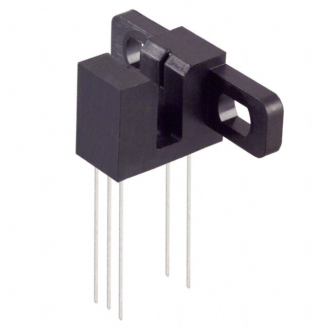
GP1S396HCP0F产品简介:
ICGOO电子元器件商城为您提供GP1S396HCP0F由Sharp Microelectronics设计生产,在icgoo商城现货销售,并且可以通过原厂、代理商等渠道进行代购。 GP1S396HCP0F价格参考。Sharp MicroelectronicsGP1S396HCP0F封装/规格:光学传感器 - 光断续器 - 槽型 - 逻辑输出, Optical Sensor Transmissive 0.047" (1.2mm) Slotted Module。您可以下载GP1S396HCP0F参考资料、Datasheet数据手册功能说明书,资料中有GP1S396HCP0F 详细功能的应用电路图电压和使用方法及教程。
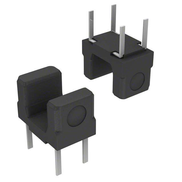
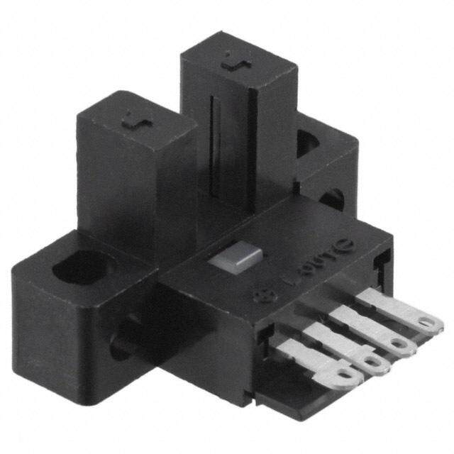
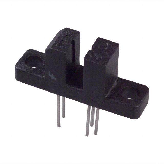
GP1S396HCP0F 是由 SHARP(现为 Socle Technology)生产的一款槽型光学断续器(光电开关),具有逻辑输出功能。该传感器广泛应用于需要非接触式检测物体存在与否的场景,尤其适用于小型设备和精密机械中。

典型应用场景包括:

1. 办公设备:如打印机、扫描仪、复印机中,用于检测纸张是否通过、卡纸检测或盖板开合状态。

2. 自动售货机:用于检测商品是否掉落、出货是否成功或投币状态检测。

3. 工业自动化设备:如装配线、传送带系统中,用于检测工件位置、计数或运动状态。

4. 家电产品:例如洗衣机、洗碗机中,用于检测门是否关闭、内部组件位置或运动状态。

5. 安防设备:用于门禁系统、自动门或红外感应装置中,实现物体或人员通过的检测。

6. 测试测量仪器:用于自动测试设备中判断被测物是否到位或移动轨迹。

该传感器具有响应速度快、可靠性高、寿命长等优点,适合空间受限、精度要求较高的场合。
| 参数 | 数值 |
| 产品目录 | |
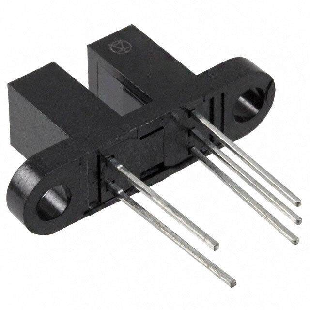
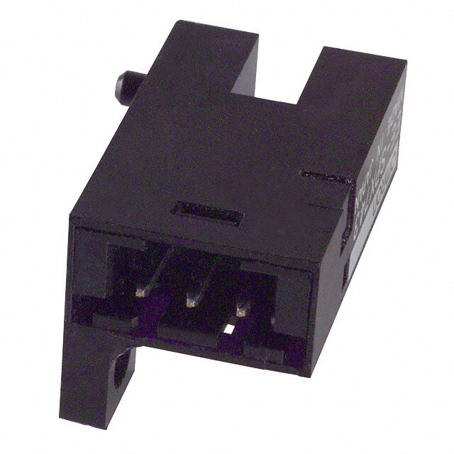
| 描述 | PHOTOINTERRUPTER OPIC SLOT 1.2MM |
| 产品分类 | |
| 品牌 | Sharp Microelectronics |
| 数据手册 | |
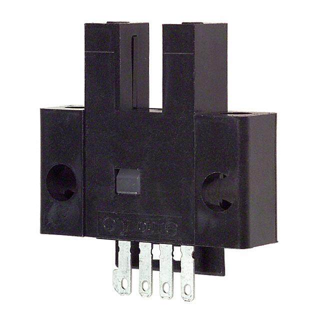
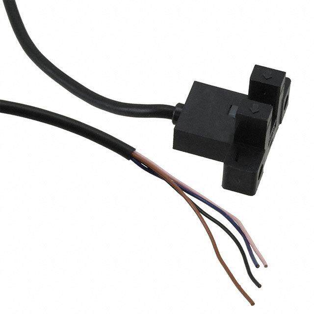
| 产品图片 |
|
| 产品型号 | GP1S396HCP0F |
| rohs | 无铅 / 符合限制有害物质指令(RoHS)规范要求 |
| 产品系列 | - |
| 其它名称 | 425-2809-1 |
| 响应时间 | - |
| 安装类型 | 通孔 |
| 封装/外壳 | 开槽模块 |
| 感应方法 | 可传导的 |
| 感应距离 | 0.047"(1.2mm) |
| 标准包装 | 1 |
| 电压-电源 | 5V |
| 电流-电源 | 100µA |
| 输出配置 | - |


PDF Datasheet 数据手册内容提取
GP1S396HCP0F GP1S396HCP0F Gap : 1.2mm Slit : 0.12mm Phototransistor Output, C ompact Transmissive Photointerrupter ■Description ■ Agency approvals/Compliance GP1S396HCP0F is a phototransistor output, 1. Compliant with RoHS directive (2002/95/EC) transmissive photointerrupter with a industry’s smallest compact and low-profile package by the thin molding technology. This product detects an object between the emitter and the detector. In addition, by narrowing the slit width of the infrared ■ Applications beam to 0.12mm, this product has improved detection accuracy. 1. General purpose detection of object presence or motion. Example : printer, lens control for camera, various mechanical position detection ■Features 1. Transmissive with phototransistor output 2. Highlights : ・Compact size ・Low Profile ・Narrow Gap 3. Key Parameters : ・Gap Width : 1.2mm ・Slit Width (detector side) : 0.12mm ・Package : 2.26 × 1.4 × 1.6mm 4. RoHS directive compliant Notice The content of data sheet is subject to change without prior notice. In the absence of confirmation by device specification sheets, SHARP takes no responsibility for any defects that may occur in equipment using any SHARP devices shown in catalogs, data books, etc. Contact SHARP in order to obtain the latest device specification sheets before using any SHARP device. Sheet No.: OP13018EN 1
GP1S396HCP0F ■Internal Connection Diagram Top View A : Anode K : Cathode C : Collector E : Emitter ■Outline Dimensions Drawing No. CY14940i02 Scale : 15/1 Unit : mm Note 1) Unspecified tolerance shall be ± 0.08mm. 2) Dimensions in parenthesis are shown for reference. 3) The dimensions indicated by ※ refer to the those measured from the lead base. 4) The dimensions shown do not include those of burrs. Burr’s dimensions shall be 0.15Max. 5) There is a possibility that the lead of part is exposed. 6) There is a possibility that the internal device is exposed at the top of the device because of the thin thickness of the outer package. 7) The mark possibly adheres partially of the side. 8) The dimension size doesn’t contain the mark thickness. Sheet No.: OP13018EN 2
GP1S396HCP0F ■Absolute maximum ratings Ta=25°C Parameter Symbol Rating Unit Forward current I 30 mA F Input Reverse voltage V 6 V R Power dissipation P 50 mW Collector-emitter voltage V 35 V CEO Emitter-collector voltage V 6 V ECO Output Collector current Ic 20 mA Collector power dissipation Pc 50 mW Total power dissipation Ptot 70 mW Operating temperature Topr -25 to +85 °C Storage temperature Tstg -40 to +100 °C * Soldering temperature Tsol 300 °C * Soldering time : 3 s or less (Hand solder.) 0.2mm or more from the bottom face of package through the substrate. Soldering area ■Electro-optical Characteristics Ta=25°C Parameter Symbol Conditions MIN. TYP. MAX. Unit Forward voltage V I =20mA - 1.2 1.4 V F F Input Reverse current I V =3V - - 10 μA R R Output Collector dark current I V =20V - - 100 nA CEO CE Collector current Ic V =5V, I =5mA 100 - 400 μA CE F Transfer Response time (Rise) tr VCE=5V, Ic=100μA - 30 120 μs character- (Fall) tf RL=1kΩ - 30 120 μs istics Collector-emitter V (sat) I =10mA, Ic=40μA - - 0.4 V saturation voltage CE F (Test circuit for response time) Vcc R Input L Test pin Output 10% 90% tr tf Sheet No.: OP13018EN 3
GP1S396HCP0F Forward current vs. ambient temperature ) A 50 m ( nt 40 e r r u c d 30 r a w r o F 20 10 5 0 -25 0 25 40 50 75 85 100 Ambient temperature Ta (°C) Power dissipation vs. ambient temperature ) W m ( ot 70 Total power dissipation Pt Pc, 50 Input and output power dissipation P, 40 n o ati 20 p si 15 s di 0 er -25 0 25 50 75 85 100 w o P Ambient temperature Ta (°C) Sheet No.: OP13018EN 4
GP1S396HCP0F Relative collector current vs. shield distance 1 (Reference value) Shield ) % ( - nt 100 90 e 0 urr 80 L c + r e elative collecto 642000 5100 Shield distanc Test condition Sensor R I =5.0mA F -1 0 1 2 3 V =5V CE Shield distance L (mm) Ta=25°C Relative collector current vs. shield distance 2 (Reference value) %) Shield ( 100 - nt 90 0 rre 80 L r cu 60 ce + o n ect 50 sta coll 40 d di Sensor ve 20 hiel ati 10 S Test condition Rel -1 0 1 2 3 IVF=5=.05mVA CE Shield distance L (mm) Ta=25°C Sheet No.: OP13018EN 5
GP1S396HCP0F ■Supplements ●ODS materials This product shall not contain the following materials. Also, the following materials shall not be used in the production process for this product. Materials for ODS : CFC , Halon, Carbon tetrachloride 1.1.1-Trichloroethane (Methyl chloroform) S ●Halogen material Chlorine < 900ppm , Bromine < 900ppm , Chlorine + Bromine < 1500ppm (Homogeneous material) ●Compliance with each regulation 1) The RoHS directive(2002/95/EC) This product complies with the RoHS directive(2002/95/EC). Object substances: mercury, lead, cadmium, hexavalent chromium, polybrominated biphenyls (PBB) and polybrominated diphenyl ethers (PBDE) 2) Content of six substances specified in Management Methods for Control of Pollution Caused by Electronic Information Products Regulation (Chinese : 电子信息产品污染控制管理办法). Toxic and hazardous substances Hexavalent Polybrominated Polybrominated Category Lead Mercury Cadmium chromium biphenyls diphenyl ethers (Pb) (Hg) (Cd) (Cr6+) (PBB) (PBDE) Photointerrupter ✓ ✓ ✓ ✓ ✓ ✓ ✓: indicates that the content of the toxic and hazardous substance in all the homogeneous materials of the part is below the concentration limit requirement as described in SJ/T 11363-2006 standard. ●Product mass : Approx. 6mg ●Country of origin : China ●Taping specification : Refer to the attachment-1. Sheet No.: OP13018EN 6
GP1S396HCP0F ■Notes ●Circuit design In circuit designing, make allowance for the degradation of the light emitting diode output that results from long continuous operation. (50% degradation/5 years) ●Prevention of detection error To prevent photointerrupter from faulty operation caused by external light, do not set the detecting face to the external light. ●Position of opaque board Opaque board shall be installed at place 0.86mm or more from the top of elements. (Example) 0.86mm or more 0.86mm or more ●Soldering Hand soldering Please solder to each lead pin at 0.2mm or more from the bottom face of package through the substrate at 300°C for 3 seconds or less. Please don't bend lead pins from the root of package when soldering. And please take care not to apply outer force to both lead pins and the package. Please don't do soldering with preheating, and please don't do soldering by reflow. In case of repairing, please make sure GP1S396HCP0F is cooled down, please consider the outer mold resin is meltdown in case a continuous heat is applied. Since the tip of the lead has exposed lead frame base material, there is a case not to be soldered. ●Cleaning Cleaning shall be carried out under the below conditions to avoid keeping solvent, solder and flux on the device. (1) Solvent cleaning : Solvent temperature 45°C or less, Immersion for 3 min. or less (2) Ultrasonic cleaning : Since the influence to the product may changes by the conditions of the ultrasonic power, time, the tank size, PCB size, the product installation condition, etc., please evaluate with actual conditions and confirm before usage. (3) The cleaning shall be carried out with solvent below. Solvent : Ethyl alcohol, Methyl alcohol ●Lead pin Lead terminals of this product have Copper, Nickel, Palladium and Gold plating. Before usage, please evaluate solder ability with actual conditions and confirm. The uniformity in color for the lead terminals are not specified. ●Storage and management after open Storage condition : Storage shall be in accordance with the below conditions. Storage temp. : 5 to 30°C Storage humidity : 70%RH or less Sheet No.: OP13018EN 7
GP1S396HCP0F ■Parts This product uses the below parts. ● Light detector (Quantity : 1) Maximum sensitivity Sensitivity Response time Type Material (nm) (nm) (μs) Silicon Phototransistor 920 700 to 1200 20 (Si) ● Light emitter (Quantity : 1) Maximum light emitting I/O Frequency Type Material wavelength (nm) (MHz) Infrared light emitting diode GaAs 940 0.3 (non-coherent) ● Material Case Lead frame Lead frame plating Black PPA resin 42 Alloy Au-Pd-Ni-Cu ● Others This product shall not be proof against radiation flux. Sheet No.: OP13018EN 8
GP1S396HCP0F ■Packing Drawing No. CY14941i09 ● Inner Packing 1) Inner Packaging drawing 2) Inner Packing material : ・Reel(PS) ・Carrier tape(PC) ・Caver tape(PET) 3) Quantity : 2,800pcs./Reel ● Outer Packaging 1) Outer Packaging drawing 2) Outer Packing material : Packing case(Corrugated cardboard ), Cushioning material(Urethane) Label(paper), Tape 3) Quantity : 14,000pcs./box 4) The contents of the carton indication conforms to EIAJ C-3 and the following items are indicated. Model No., Internal production control name, Quantity, Packing date, Corporate name, Country of origin 5) Regular packaged mass : Approximately 500g Sheet No.: OP13018EN 9
GP1S396HCP0F (Attachment-1-1) Package specifications (φ180mm reel) 1) Application This specification applies to the taping specifications and the relation items for the GP1S396HCP0F. 2) Taping method (1) Tape structure and Dimensions (Refer to the attached sheets-1-2) The tape shall have a structure in which a cover tape is sealed pressed on the carrier tape made by polycarbonate to protect against static electricity. (2) Reel structure and Dimensions (Refer to the attached sheets-1-3) (3) Direction of product insertion (Refer to the attached sheets-1-3) Product direction in carrier tape shall direct to the detector at the hole side on the tape. 3) Repair method of sealing error In case of repairing a sealing error, three sides of a cover tape matching to the product insertion portion are opened by a cutter and it will be closed by adhesiveness tape after repairing. 4) Adhesiveness of cover tape The exhalation force between carrier tape and cover tape shall be 0.1N to 1.0N for the angle from 165° to 180°. 5) Rolling method and quantity (1) Wind the tape back on the reel so that the cover tape will be outside the tape. (2) Attach more than 16cm of blank tape to the trailer and attach more than 10cm of the leader. Attach more than 40cm of cover tape to the leader to the tape and fix the both ends with adhesive tape. (3) One reel shall contain 2,800 pcs. 6) Indication items The contents of the carton indication conforms to EIAJ C-3 and the following items are indicated. Model No., Internal production control name, Quantity, Packing date, Corporate name, Country of origin 7) Safety protection during shipping There shall be no deformation of component or degradation of electrical characteristics due to shipping. Sheet No.: OP13018EN 10
GP1S396HCP0F (Attachment-1-2) ● Tape structure and dimensions Sheet No.: OP13018EN 11
GP1S396HCP0F (Attachment-1-3) ● Reel structure and dimensions ● Direction of product insertion Sheet No.: OP13018EN 12
GP1S396HCP0F ■Important Notices · The circuit application examples in this publication are provided with equipment that requires higher reliability such as: to explain representative applications of SHARP devices and are --- Transportation control and safety equipment (i.e., not intended to guarantee any circuit design or license any aircraft, trains, automobiles, etc.) intellectual property rights. SHARP takes no responsibility for --- Traffic signals any problems related to any intellectual property right of a third --- Gas leakage sensor breakers party resulting from the use of SHARP's devices. --- Alarm equipment --- Various safety devices, etc. · Contact SHARP in order to obtain the latest device specification (iii) SHARP devices shall not be used for or in connection with sheets before using any SHARP device. SHARP reserves the equipment that requires an extremely high level of reliability and right to make changes in the specifications, characteristics, data, safety such as: materials, structure, and other contents described herein at any --- Space applications time without notice in order to improve design or reliability. --- Telecommunication equipment [trunk lines] Manufacturing locations are also subject to change without --- Nuclear power control equipment notice. --- Medical and other life support equipment (e.g., scuba). · Observe the following points when using any devices in this publication. SHARP takes no responsibility for damage caused · If the SHARP devices listed in this publication fall within the by improper use of the devices which does not meet the scope of strategic products described in the Foreign Exchange conditions and absolute maximum ratings to be used specified in and Foreign Trade Law of Japan, it is necessary to obtain the relevant specification sheet nor meet the following approval to export such SHARP devices. conditions: (i) The devices in this publication are designed for use in general · This publication is the proprietary product of SHARP and is electronic equipment designs such as: copyrighted, with all rights reserved. Under the copyright laws, --- Personal computers no part of this publication may be reproduced or transmitted in --- Office automation equipment any form or by any means, electronic or mechanical, for any --- Telecommunication equipment [terminal] purpose, in whole or in part, without the express written --- Test and measurement equipment permission of SHARP. Express written permission is also --- Industrial control required before any use of this publication may be made by a --- Audio visual equipment third party. --- Consumer electronics (ii) Measures such as fail-safe function and redundant design · Contact and consult with a SHARP representative if there are should be taken to ensure reliability and safety when SHARP any questions about the contents of this publication. devices are used for or in connection Sheet No.: OP13018EN 13