ICGOO在线商城 > GM5SAE35P0A

 Datasheet下载
- 型号: GM5SAE35P0A
- 制造商: Sharp Microelectronics
- 库位|库存: xxxx|xxxx
- 要求:
| 数量阶梯 | 香港交货 | 国内含税 |
| +xxxx | $xxxx | ¥xxxx |
查看当月历史价格
查看今年历史价格
GM5SAE35P0A产品简介:
ICGOO电子元器件商城为您提供GM5SAE35P0A由Sharp Microelectronics设计生产,在icgoo商城现货销售,并且可以通过原厂、代理商等渠道进行代购。 提供GM5SAE35P0A价格参考以及Sharp MicroelectronicsGM5SAE35P0A封装/规格参数等产品信息。 你可以下载GM5SAE35P0A参考资料、Datasheet数据手册功能说明书, 资料中有GM5SAE35P0A详细功能的应用电路图电压和使用方法及教程。
| 参数 | 数值 |
| 产品目录 | |
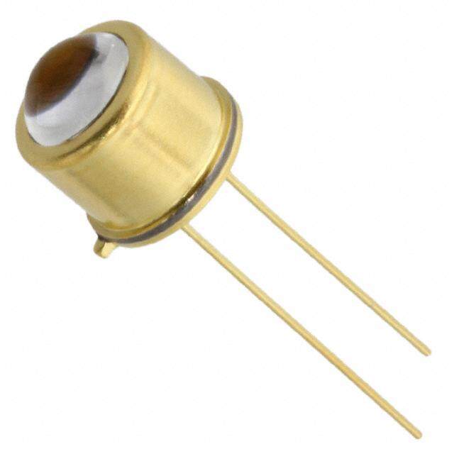
| 描述 | LED WHITE 3500K 20MA 3.2V PLCC2 |
| 产品分类 | |
| 品牌 | Sharp Microelectronics |
| 数据手册 | |
| 产品图片 |
|
| 产品型号 | GM5SAE35P0A |
| PCN过时产品 | http://www.sharpsma.com/download/PCN-2012-1218-01pdf |
| rohs | 无铅 / 符合限制有害物质指令(RoHS)规范要求 |
| 产品系列 | - |
| 产品目录绘图 |
|
| 产品目录页面 | |
| 其它名称 | 425-2746-6 |
| 包装 | Digi-Reel® |
| 大小/尺寸 | 3.20mm 长x 2.80mm 宽 |
| 安装类型 | 表面贴装 |
| 封装/外壳 | 2-PLCC |
| 标准包装 | 1 |
| 毫烛光等级 | 2100mcd |
| 波长-主 | 3500K |
| 波长-峰值 | - |
| 测试电流时的光通量 | 6 lm |
| 电压-正向(Vf)(典型值) | 3.2V |
| 电流-测试 | 20mA |
| 视角 | - |
| 透镜样式/尺寸 | 圆形,带平顶,2.4mm |
| 透镜类型 | 散射,有色 |
| 颜色 | 暖白色 |
| 高度 | 1.90mm |


- 商务部:美国ITC正式对集成电路等产品启动337调查
- 曝三星4nm工艺存在良率问题 高通将骁龙8 Gen1或转产台积电
- 太阳诱电将投资9.5亿元在常州建新厂生产MLCC 预计2023年完工
- 英特尔发布欧洲新工厂建设计划 深化IDM 2.0 战略
- 台积电先进制程称霸业界 有大客户加持明年业绩稳了
- 达到5530亿美元!SIA预计今年全球半导体销售额将创下新高
- 英特尔拟将自动驾驶子公司Mobileye上市 估值或超500亿美元
- 三星加码芯片和SET,合并消费电子和移动部门,撤换高东真等 CEO
- 三星电子宣布重大人事变动 还合并消费电子和移动部门
- 海关总署:前11个月进口集成电路产品价值2.52万亿元 增长14.8%


PDF Datasheet 数据手册内容提取
Preliminary GM5SAExxP0A (Series) GM5SAExxP0A Light Emitting Diode (Series) ■Features ■Agency Approvals/Compliance 1. Single-chip device, the given output at I =20 mA 1. RoHS compliant F 2. White Color, high color rendering (achieved via Blue LED chip in combination with red and green phosphors) ■Applications 3. Luminous flux: 6.0 lm 1. General lighting 4. Lumens per watt: 90 to 105 2. General indication (indoor use only) 5. Eight devices, covering a number of color temper- 3. Office Automation equipment ature ranges: 4. Audio/visual equipment 5. Home appliances Color Luminous Part Number Temperature (K) Intensity (mcd) 6. Telecommunications equipment GM5SAE65P0A 6500 (2200) 7. Measuring equipment GM5SAE57P0A 5700 (2200) 8. Machine tools GM5SAE50P0A 5000 (2200) 9. Computers GM5SAE45P0A 4500 (2200) GM5SAE40P0A 4000 (2150) GM5SAE35P0A 3500 (2100) GM5SAE30P0A 3000 (2050) GM5SAE27P0A 2700 (2000) Notice The content of data sheet is subject to change without prior notice. In the absence of confirmation by device specification sheets, SHARP takes no responsibility for any defects that may occur in equipment using any SHARP devices shown in catalogs, data books, etc. Contact SHARP in order to obtain the latest device specification sheets before using any SHARP device. 1 Sheet No.: DG-091008 Date March, 2009 ©SHARP Corporation
Preliminary GM5SAExxP0A (Series) ■External Dimensions 3.5 3.2 (2.4) 8 2) 2. 2. ( 1 2 Cathode Mark 8) 0. ( 9 1. 5) 1 Equivalent Circuit 0. ( Tc 1 2 Pin Arrangement No. Name 1 Anode (1.9) 2 Cathode NOTES: 1. Units: mm 2. Unspecified tolerence: ±0.3 mm 3. ( ): Reference dimensions 4. Case temperature (Tc) measurement point 5. Materials: Package: Nylon and Silicone resin Leads: Copper Alloy, Ag plating GM5SAExxP0A-1 Sheet No.: DG-091008 2
Preliminary GM5SAExxP0A (Series) ■Absolute Maximum Ratings (Tc = 25°C, unless noted) Parameter Symbol Rating Unit Power dissipation (Package total) *1 P 111 mW Power dissipation derating factor *2 2.22 mW/°C Forward current *1 I 30 mA F Peak pulsed forward current *3 I 100 mA FM DC *2 0.60 mA/°C Forward current derating factor *7 Pulse *1 2.0 mA/°C Reverse current I 70 mA R Junction Temperature *4 Tj 125 °C Operating temperature *5 Tc -30 to +100 °C Storage temperature *6 Tstg -40 to +100 °C Soldering temperature *7 Tsol 295 °C *1 Temperature range: -30°C ≤ Tc ≤ 60°C *2 Temperature range: 60°C < Tc ≤ 100°C *3 Duty ratio = 1/10, Pulse width = 0.1 ms *4 Thermal resistance, junction-to-case = 95°C/W *5 Case temperature (See External Dimensions on page 2); This device uses the leads for heat sinking, therefore the operating temperature range is prescribed by Tc. *6 Do not exceed these temperatures under any condition, not even while in packing. Refer to Storage and Handling. *7 Each terminal must be soldered with a 30 W soldering iron within 3 seconds under 295°C. For Reflow Soldering information, see Fig. 16. *8 Operating current values here follow the derating curves shown in Fig. 1 through Fig. 3. (Tc = 25°C) ■Electro-optical Characteristics Parameter Symbol Conditions MIN. TYP. MAX. Unit Forward voltage V — (3.2) 3.7 V F Luminous intensity I (1530) *1 (3160) mcd V Luminous flux φv 6.0 lm I = 20 mA F Lumens per watt lm/W 90 105 Chromaticity coordinates x, y *2 Color Rendering Index R — (80) — a *1 See Characteristics by Model table. *2 See Chromaticity Ranking Table. ●Characteristics by Model Chromaticity Color Temperature Chromaticity Luminous Part Number Coordinates (K) Rank Intensity (TYP.) GM5SAE65P0A 6500 (0.314, 0.324) a, b (2200) GM5SAE57P0A 5700 (0.328, 0.337) b, c (2200) GM5SAE50P0A 5000 (0.345, 0.352) c, d (2200) GM5SAE45P0A 4500 (0.361, 0.364) d, e (2200) GM5SAE40P0A 4000 (0.381, 0.377) e, f, g1, g2 (2150) GM5SAE35P0A 3500 (0.405, 0.391) g1, g2, h1, h2 (2100) GM5SAE30P0A 3000 (0.437, 0.404) j1, j2 (2050) GM5SAE27P0A 2700 (0.460, 0.411) k1, k2 (2000) *1 Measured by EG&G Model 550 (Radiometer/Photometer) after 20 ms drive (Tolerance: ±15%) See the Luminosity Rank table for ranking range details. *2 Measured by Otsuka Electronics Model MCPD-2000 after 20 ms drive (Tolerance: x, y: ±0.02). See the Chromaticity Rank table for ranking range details; quantities of any given rank are decided by Sharp. * 3 Parens indicate reference values. Sheet No.: DG-091008 3
Preliminary GM5SAExxP0A (Series) ■Derating Curves Fig. 3 Peak Pulsed Forward Current vs. Case Temperature Fig. 1 Forward Current vs. A) 120 m Case Temperature (M F 100 70 nt I e 60 Curr 80 nt I (mA)F 4500 d Forward 4600 e e Curr 30 Puls 20 d k orwar 20 Pea -040-30-20 0 20 40 60 80 100 120 F 10 Case Temperature Tc (°C) 0 GM5SAExxP0A-4 -40-30-20 0 20 40 60 80 100 120 Case Temperature Tc (°C) Fig. 4 Power Dissipation GM5SAExxP02-3 vs. Case Temperature 120 Fig. 2 Peak Pulsed Forward Current vs. Duty Ratio W) 100 m (Tc = 25°C) P ( 80 mA) 120 pation 60 (M 100 ssi Current IF 80 Power Di 2400 d ar 60 0 orw -40-30-20 0 20 40 60 80 100 120 d F 40 Case Temperature Tc (°C) e s ul P 20 k GM5SAExxP0A-6 a e P 0 1/100 1/10 1 Duty Ratio GM5SAExxP0A-5 Sheet No.: DG-091008 4
Preliminary GM5SAExxP0A (Series) ■Characteristic Diagrams (TYP.) Fig. 7 Relative Luminous Intensity Characteristics data are typical data and so are not guaranteed data. vs. Case Temperature (I = 20 mA) Fig. 5 Relative Luminous Intensity F 1000 vs. Forward Current (Tc = 25°C) %) 1000 y ( sit n %) nte y ( s I ntensit 100 minou 100 s I Lu minou ative u el e L 10 R v ati el R 10 -30-20-10 0 10 20 30 40 50 60 70 80 90100 1 Case Temperature Tc (°C) 0.1 1 10 100 GM5SAExxP0A-9 Forward Current I (mA) F GM5BW5SAExxP0A-7 Fig. 6 Forward Current vs. Forward Voltage (Tc = 25°C) 100 A) m (F 10 nt I e urr C d ar 1 w or F 0.1 2.2 2.7 3.2 3.7 Forward Voltage V (V) F GM5SAExxP0-8 Sheet No.: DG-091008 5
Preliminary GM5SAExxP0A (Series) ■Chromaticity Rank Table (Tc = 25°C) Chromaticity Coordinates (x, y) Rank Point 1 Point 2 Point 3 Point 4 Condition x y x y x y x y a 0.293 0.322 0.301 0.293 0.314 0.306 0.309 0.339 b 0.309 0.339 0.314 0.306 0.329 0.319 0.328 0.357 c 0.328 0.357 0.329 0.319 0.343 0.331 0.347 0.374 d 0.347 0.374 0.343 0.331 0.357 0.341 10.365 0.388 e 0.365 0.388 0.357 0.341 0.370 0.350 0.383 0.400 f 0.383 0.400 0.367 0.350 0.382 0.357 0.398 0.410 g 0.398 0.410 0.382 0.357 0.395 0.364 0.416 0.420 g1 0.398 0.410 0.390 0.382 0.405 0.391 0.416 0.420 I = 20 mA F g2 0.340 0.382 0.382 0.357 0.395 0.364 0.405 0.391 h1 0.416 0.420 0.405 0.391 0.423 0.399 0.437 0.430 h2 0.405 0.391 0.395 0.364 0.411 0.371 0.423 0.399 j1 0.437 0.430 0.423 0.399 0.452 0.409 0.469 0.441 j2 0.423 0.399 0.411 0.371 0.436 0.379 0.452 0.409 k1 0.469 0.441 0.452 0.409 0.477 0.414 0.497 0.447 k2 0.452 0.409 0.436 0.379 0.459 0.384 0.477 0.414 *1 Tolerance: ±0.02. *2 Shipment quantities of each rank may not be specified by the Customer. Fig. 8 Chromaticity Diagram 3000K (j1, j2) 2800 - 5000K Δuv = ±0.01 0.45 4000K (e, f, g1, g2) 3500 - 4500K 0.43 Δuv = ±0.01 5000K (c, d) k1 Black Body 4500 - 5700K j1 0.41 Δuv = ±0.01 h1 Locus k2 0.39 6500K (a, b) g1 j2 5700 - 7800K f h2 Δuv = ±0.01 e g2 0.37 d 2700K (k1, k2) y 0.35 c 2500 - 2800K b 3500K (g1, g2, h1, h2) Δuv = ±0.01 0.33 3100 - 3800K a 4500K (d, e) Δuv = ±0.01 0.31 4100 - 5000K Δuv = ±0.01 0.29 5700K (b, c) 5000 - 6600K 0.27 Δuv = ±0.01 0.25 0.28 0.30 0.32 0.34 0.36 0.38 0.40 0.42 0.44 0.46 0.48 0.50 x GM5SAExxP0A-2 Sheet No.: DG-091008 6
Preliminary GM5SAExxP0A (Series) ■Design Notes 1. Do not allow the circuit to apply any reverse voltage to the LEDs at any time, operating or not. Do not bias this part in any manner when it is not operating. Reverse voltage can also be induced via EMF, generated by ambi- ent light falling on this part. When these parts are operated in series, connect a zener diode parallel to each part to protect them from reverse voltage. 2. This part can be damaged by mechanical stress. Be certain that assembly steps do not stress this part; pay particular attention to pick-and-place equipment. Verify placing pressure and do not allow the collet to contact the resin of this part. 3. This product uses blue LED chips in combination with yellow phosphor to achieve its color. There may be some slight color change due to afterglow of the phosphor when driving this part with pulsed power. 4. This part has a high light output. Looking directly at it during full power output may cause injury. 5. Sharp recommends taking proper personal and environmental static control precautions when handling this part. 6. This device incorporates thermally conductive materials to allow heat to be transferred from it to the circuit board. For best reliability, do not locate other sources of heat near the LED, and design the circuit board for effective heat dissipation. Keep the part’s case temperature under 100°C (LED ON) including self-heating. 7. Handle these parts in a clean environment; dust may be difficult to remove and can affect optical performance. 8. Confirm the part’s performance, reliability, and resistance to degradation, if exposing it to these environments: (cid:129)Direct sunlight, outdoor exposure, dusty conditions (cid:129)In water, oil, medical fluids, and organic solvents (cid:129)Excessive moisture, such as dew or condensation (cid:129)Corrosive (salt) air or corrosive gases, such as Cl, H S, NH , SO , NO 2 3 2 X Sheet No.: DG-091008 7
Preliminary GM5SAExxP0A (Series) ■Reliability and Quality Information Sharp tests to a Reliability Confidence Level of 90%. These tables illustrate the test criteria and conditions, along with the Number of Samples, the Number of Defectives, and the Lot Tolerance Percent Defective. Samples Defective LTPD No. Test Items Test Conditions (n) (C) (%) 1 Temperature cycle -40°C (30 min) to +100°C (30 min), 100 cycles 22 0 10 2 High temp and high humidity storage Tstg = +60°C, RH = 90%, t = 1000 hr 22 0 10 3 High temperature storage Tstg = +100°C, t = 1000 hr 22 0 10 4 Low temperature storage Tstg = -40°C, t = 1000 hr 22 0 10 5 Operating test Tc = +60°C, I = 30 mA, t=1000 hr 22 0 10 F 15000 m/s2, 0.5 ms ±X (cid:129) ±Y (cid:129) ±Z direction, 6 Mechanical shock 11 0 20 3 times (Tc = 25°C) 200 m/s2, 100 to 2000 to 100 Hz / sweep for 7 Variable frequency vibration 11 0 20 4 min. X (cid:129) Y (cid:129) Z direction, 4 times (Tc = 25°C) 8 Resistance to soldering temperatures Refer to the Soldering Profile; Performed twice 11 0 20 Solder/flux M705/ESR250 (Senju Metal Indus- 9 Solderability try Co. Ltd.) Soldering temperature 245°C ±5°; 11 0 20 dip time 3 sec, after 150°C exposure for 1 hr HBM 1 kV 10 Electrostatic Discharge 11 0 20 (EIAJ ED-4710 test method 304 compliant) ●Failure Judgement Criteria No. Items Symbol Failure judgment criteria (*2) 1 Forward voltage V V > U.S.L × 1.2 F F 2 Reverse current I I > U.S.L × 2.0 R R 3 Luminous intensity (*3) Iv Iv < Initial value × 0.5, Iv > Initial value × 2.0 *1 Measuring condition is in accordance with specification. *2 U.S.L.: Upper Specification Limit. *3 Solderability failure criterion: Fail if >90% solderability in plated test areas are not soldered. Judgement areas are the bottom and sides as shown in Fig. 9, excluding 0.3 mm from lead bends. Fig. 9 Solderability Judgment Areas 0.3 mm 0.3 mm 0.3 mm Lead Bends GM5SAExxP0-10 Sheet No.: DG-091008 8
Preliminary GM5SAExxP0A (Series) ●Lifetime Data Mean lifetime: 40,000 hr Conditions: Tc = 60°C, I = 20 mA F Criterion: Iv < Initial value × 0.7 1. Lifetime Data Estimation Methods Luminous intensity variation data is acquired during a 3,000-hour accelerated test, with the conditions of Tc = 70 to 110°C, and I = 15 to 30 mA. F Using data points gathered from 1,000 to 3,000 hours, the value τ (which is the point of 70% decrease in luminous output) is calculated based on the linear regression of the relationship between the luminous intensity maintenance ratio and the square root of the time. An Arrhenius plot of the Mean Lifetime is generated by plotting case tempera- ture and the value τ. Therefore the Lifetime Estimate becomes the 70% decrease of the initial luminous intensity at 50°C. ●Quality Level Sharp utilizes the IS02859-1 standard when measuring product quality. The method is a single sampling plan, following normal inspection level S-4. This table lists the Defect Judgment Criteria and Defect Classifications. No. Test Items Defect Judgment Defect AQL 1 Light emission No light emission 2 Radiation color Different color vs. that prescribed in the Chromaticity Chart Major defect .0.1% 3 Taping Product inserted incorrectly (anything not as specified) 4 Electro-optical characteristics Does not fully conform to specification values for V or I . F V Does not fully conform to specification values for 5 External dimensions External Dimensions Minor defect 0.4% Foreign substances and flaws which affect the appearance: 6 Appearance Resin burr which exceeds tolerance, (±0.3 mm MAX.) More than 0.4 mm cracks in resin or terminal Sheet No.: DG-091008 9
Preliminary GM5SAExxP0A (Series) ■Tape Specifications Fig. 10 Tape Shape and Dimensions 7 . P 1 0 t 1 D A 0 Cathode E F 0 W 1 B W t3 P2 Anode t 2 P 1 GM5SAExxP0A-11 ■Tape Dimension Specifications Dimension Parameter Symbol Remarks (mm) Vertical A 3.0 Measured at inside bottom square corner Embossed pocket Horizontal B 3.7 Pitch P 4.0 1 Diameter D 1.5 0 Sprocket hole Pitch P 4.0 Accumulated error ±0.5 mm/10 pitch 0 Position E 1.75 Distance between the edge of the tape and center of the hole Vertical P2 2.0 Distance between center lines of the concave square hole and Pocket Position Horizontal F 3.5 round sprocket hole Width W 5.4 1 Cover tape Thickness t 0.1 3 Width W 8.0 0 Carrier tape Thickness t 0.3 1 Overall thickness t 2.6 Includes thickness of cover tape and carrier tape 2 Sheet No.: DG-091008 10
Preliminary GM5SAExxP0A (Series) ■Reel Specifications Fig. 11 Reel Shape and Dimensions 0.8 0.6 0.4 0.2 E U C B A SHARP CORPORATION PART No. QUANTITY LOT No. RANK 〈EIAJ C-3〉MADE IN PHILIPPINES Label (Example) t W GM5SAExxP0A-12 ■Reel Dimension Specifications Parameter Symbol Dimension (mm) Remarks Diameter A 180 Flange Thickness t 1.3 Flange spacing W 9.5 Shaft core dimension External diameter B 60 Spindle hole diameter C 13 Hub Key slit width E 2.0 Key slit depth U 4 *1 Label on side of flange: part number, quantity, lot number, and rank. *2 Material: described on flange. Sheet No.: DG-091008 11
Preliminary GM5SAExxP0A (Series) ■Taping Specifications 1. Leader tape standard: JIS C0806 Fig. 12 Leader Tape Pull out Beginning End Empty Stuffed Leader (Empty) 40 mm MIN. 400 mm MIN. GM5SAExxP0A-13 2. Cover tape peel resistance: F = 0.1 to 1.0 N (θ = 10° or less). See Fig. 10. Fig. 13 Tape Separation F Cover tape θ = 0 ~ 10° Tape speed: 5 mm/s Forward Carrier tape GM5SAExxP0A-14 3. Tape bending resistance: Cover tape will remain in place on radii of 30 mm or more. Under 30 mm radii, the cover may separate. 4. Joints are not allowed in the cover tape. 5. Parts are packed with an average quantity of 2000 pieces per reel. 6. Product mass: 30 mg (approximately) 7. Sharp guarantees the following: a. No contiguous empty spaces in the tape b. Missing parts will not make up more than 0.1% of the total quantity. c. Parts will be easily removed from the tape. 8. Parts will not stick to the cover tape as it is peeled. Sheet No.: DG-091008 12
Preliminary GM5SAExxP0A (Series) ■Label and Marking Information Fig. 14 Label Contents SHARP CORPORATION PART No. GM5SAExxP0A ←Part number QUANTITY 2000 ← Quantity ← EIAJ C-3 Bar code ←EIAJ C-3 Bar code LOT No. MI08A01 RANK ←Lot number and rank 〈EIAJ C-3〉MADE IN PHILIPPINES ←Production country LOT Number MI 0 8 A 0 1 1 2 3 4 1 Production plant code (alphabetically) 2 Production year (the last two digits of the year) 3 Production month (alphabetically with January corresponding to A) 4 Production date (01 ~ 31) Rank : Chromaticity rank GM5SAExxP0A-15 ■Manufacturing Guidelines ●Storage and Handling 1. Moisture-proofing: These parts are shipped in vacuum-sealed bags to keep them dry and ready for use. See Fig. 15. 2. Store these parts between 5°C and 30°C, at a relative humidity of less than 70%; for no more than one year from the production date. 3. After breaking the package seal, maintain the environment within 5°C to 30°C, at a relative humidity of less than 60%. Solder the parts within 3 days. 4. If the parts will not be used immediately, repack them in a dry box, or re-vacuum-seal them with a desiccant. 5. If the parts are exposed to air for more than 3 days, or if the silica gel telltale indicates moisture contamination, bake the parts: (cid:129)When in the tape carrier, bake them at a temperature of 95°C to 100°C, for 16 to 24 hours. (cid:129)When loose or on a PCB, bake them at a temperature of 110°C to 120°C, for 8 to 12 hours. (cid:129)Note that the reels may become distorted if they are in a stack when baking. Confirm that the parts have cooled to room temperature after baking. ●Cleaning Instructions 1. Sharp does not recommend cleaning printed circuit boards containing this device, or cleaning this device with ultrasonic methods. Process chemicals will affect the structural and optical characteristics of this device. 2. Sharp recommends the use of a solder paste that does not require cleaning. 3. Do not clean this part ultrasonically. Sheet No.: DG-091008 13
Preliminary GM5SAExxP0A (Series) Fig. 15 Factory Moisture-proof Packing Label Aluminum bag Silica gel Reel Label (EIAJ-compliant) GM5SAExxP0A-16 ●Soldering Instructions 1. When soldering with reflow methods, Sharp recommends following the soldering profile in Fig. 16. 2. Do not subject the package to excessive mechanical force during soldering as it may cause deformation or defects in plated connections. Internal connections may be severed due to mechanical force placed on the pack- age due to the PCB flexing during the soldering process. 3. When using a second reflow, the second process should be carried out as soon as possible after the first. Stor- age in a dry box is recommended between reflows. 4. Electrodes on this part are silver-plated. If the part is exposed to a corrosive environment, the plating may be damaged, thereby affecting solderability. 5. The Reflow Profile shown in Fig. 16 should be considered as a set of maximum parameters. Since this part uses the leads for heatsinking, the peak temperature should be kept as cool as possible and the cooldown period lengthened as much as possible. Thermal conduction into the LED will be affected by the performance of the reflow process, so verification of the reflow process is recommended. These parts may be used in a nitrogen reflow process. Fig. 16 Temperature Profile 260 (MAX.) 1 ~ 2.5°C/s C) 220 1 ~ 4°C/s ° e ( 200 ur 60s (MAX) erat 150 p m 60 ~ 120s e 5s (MAX) T 1 ~ 4°C/s 25 Time (s) GM5SAExxP0A-17 Sheet No.: DG-091008 14
Preliminary GM5SAExxP0A (Series) ●Recommended Solder Pad Design 1. Solderability depends on reflow conditions, solder paste, and circuit board materials. Check the entire process before production commences. 2. Fig. 17 shows the recommended solder pad design for this part. 3. When using backside dip methods, Sharp recommends checking the process carefully: board warping from heat can cause mechanical failure in these parts, in addition to the high heat conducted into the part through the leads. Performing reflow after dip is recommended, with the interval between the two as short as possible. Fig. 17 Recommended Solder Pad Design Product center 6 2. 1.5 1.5 4.5 NOTE: Unit: mm GM5SAExxP0A-18 ●Pick and Place Recommendations 1. Picking errors can occur based on the machine’s setup, so Sharp recommends verification with the machine in actual use. 2. Do not allow the pick and place machine to contact the sealing resin in this part. If mechanical stress is placed on the sealing resin, such forces can cause the resin to fail, or cause bonding wires within the part to break. ■Presence of ODCs This product shall not contain the following materials, and they are not used in the production process for this product: (cid:129)Regulated substances: CFCs, Halon, Carbon tetrachloride, and 1,1,1-Trichloroethane (Methylchloroform). Specific brominated flame retardants such as the PBBOs and PBBs are not used in this product at all. This product shall not contain the following materials banned in the RoHS Directive (2002/95/EC). (cid:129)Lead, Mercury, Cadmium, Hexavalent chromium, Polybrominated biphenyls (PBB), Polybrominated diphenyl ethers (PBDE). Sheet No.: DG-091008 15
Preliminary GM5SAExxP0A (Series) ■Important Notices ---Transportation control and safety equipment (i.e., aircraft, trains, automobiles, etc.) · The circuit application examples in this publication are ---Traffic signals provided to explain representative applications of ---Gas leakage sensor breakers SHARP devices and are not intended to guarantee any ---Alarm equipment circuit design or license any intellectual property rights. ---Various safety devices, etc. SHARP takes no responsibility for any problems (iii) SHARP devices shall not be used for or in connec- related to any intellectual property right of a third party tion with equipment that requires an extremely high resulting from the use of SHARP’s devices. level of reliability and safety such as: ---Space applications · Contact SHARP in order to obtain the latest device ---Telecommunication equipment (trunk lines) specification sheets before using any SHARP device. ---Nuclear power control equipment SHARP reserves the right to make changes in the ---Medical and other life support equipment (e.g. specifications, characteristics, data materials, struc- scuba) ture, and other contents described herein at any time without notice in order to improve design or reliability. · If the SHARP devices listed in this publication fall Manufacturing locations are also subject to change within the scope of strategic products described in the without notice. Foreign Exchange and Foreign Trade Law of Japan, it is necessary to obtain approval to export such SHARP · Observe the following points when using any devices devices. in this publication. SHARP takes no responsibility for damage caused by improper use of the devices which · This publication is the proprietary product of SHARP does not meet the conditions and absolute maximum and is copyrighted, with all rights reserved. Under the ratings to be used specified in the relevant specification copyright laws, no part of this publication may be repro- sheet nor meet the following conditions: duced or transmitted in any form or by any means, (i) The devices in this publication are designed for use electronic or mechanical, for any purpose, in whole or in general electronic equipment designs such as: in part, without the express written permission of ---Personal computers SHARP. Express written permission is also required ---Office automation equipment before any use of this publication may be made by a ---Telecommunication equipment (terminal) third party. ---Test and measurement equipment ---Industrial control · Contact and consult with a SHARP representative if ---Audio visual equipment there are any questions about the contents of this pub- ---Consumer electronics lication. (ii) Measures such as fail-safe function and redundant design should be taken to ensure reliability and safety when SHARP devices are used for or in connection with equipment that requires higher reliabilty such as: Sheet No.: DG-091008 16