ICGOO在线商城 > 隔离器 > 隔离器 - 栅极驱动器 > FOD8321R2V
 Datasheet下载
- 型号: FOD8321R2V
- 制造商: Fairchild Semiconductor
- 库位|库存: xxxx|xxxx
- 要求:
| 数量阶梯 | 香港交货 | 国内含税 |
| +xxxx | $xxxx | ¥xxxx |
查看当月历史价格
查看今年历史价格
FOD8321R2V产品简介:
ICGOO电子元器件商城为您提供FOD8321R2V由Fairchild Semiconductor设计生产,在icgoo商城现货销售,并且可以通过原厂、代理商等渠道进行代购。 FOD8321R2V价格参考。Fairchild SemiconductorFOD8321R2V封装/规格:隔离器 - 栅极驱动器, 3A Gate Driver Optical Coupling 5000Vrms 1 Channel 5-SOP。您可以下载FOD8321R2V参考资料、Datasheet数据手册功能说明书,资料中有FOD8321R2V 详细功能的应用电路图电压和使用方法及教程。
FOD8321R2V 是安森美半导体(ON Semiconductor)生产的一款栅极驱动光耦,属于隔离型栅极驱动器。其主要应用场景包括:

1. 开关电源(SMPS):适用于各种高电压、高频率的开关电源系统,如AC-DC转换器、DC-DC转换器,用于驱动MOSFET或IGBT等功率开关器件,提供输入与输出之间的电气隔离,提高系统安全性与稳定性。

2. 电机控制:在工业自动化、电机驱动器、变频器等应用中,FOD8321R2V可用来驱动功率晶体管,实现控制电路与功率电路之间的隔离,防止高压干扰或损坏控制电路。

3. 新能源系统:如光伏逆变器、储能系统、电动汽车充电设备等,该器件能够在高压与低压电路之间提供可靠的信号传输和驱动能力,保障系统在复杂电磁环境下的稳定运行。

4. 家电控制:部分高端家电产品如变频空调、电磁炉等中,也用于隔离控制电路与功率电路,提升整机安全性和抗干扰能力。

该器件采用双列直插封装(DIP),具备高隔离电压、快速响应时间和较强的抗干扰能力,适用于需要电气隔离和高效驱动的多种工业与消费类电子系统。
| 参数 | 数值 |
| 产品目录 | |
| 描述 | ISOLAT IGBT DVR 4.24KVRMS 5SOPMOSFET输出光电耦合器 Dual 2A High-Speed Low-Side Gate Driver |
| 产品分类 | |
| 品牌 | Fairchild Semiconductor |
| 产品手册 | |
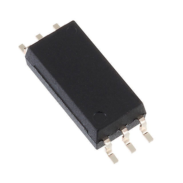
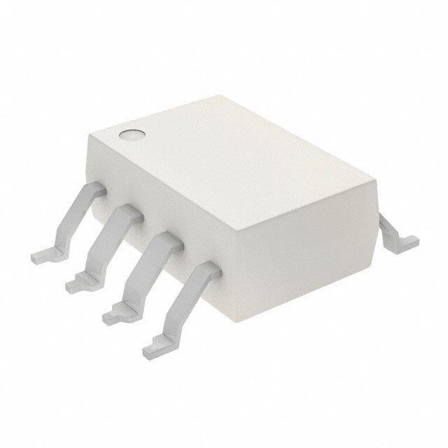
| 产品图片 |
|
| rohs | 符合RoHS无铅 / 符合限制有害物质指令(RoHS)规范要求 |
| 产品系列 | 光耦合器/光电耦合器,MOSFET输出光电耦合器,Fairchild Semiconductor FOD8321R2VOPTOPLANAR® |
| 数据手册 | |
| 产品型号 | FOD8321R2V |
| PulseWidthDistortion(Max) | 300ns |
| 上升/下降时间(典型值) | 60ns, 60ns |
| 不同If时的传播延迟高-低 | 300ns |
| 产品种类 | MOSFET输出光电耦合器 |
| 传播延迟tpLH/tpHL(最大值) | 500ns, 500ns |
| 供应商器件封装 | 5-SOP |
| 共模瞬态抗扰度(最小值) | 20kV/µs |
| 其它名称 | FOD8321R2VDKR |
| 包装 | Digi-Reel® |
| 单位重量 | 400 mg |
| 商标 | Fairchild Semiconductor |
| 安装类型 | 表面贴装 |
| 封装 | Reel |
| 封装/外壳 | 6-SOIC (0.346", 8.80mm 宽)5 引线 |
| 封装/箱体 | SO-5 |
| 工作温度 | -40°C ~ 100°C |
| 工厂包装数量 | 1000 |
| 技术 | 光学耦合 |
| 数据速率 | - |
| 最大功率耗散 | 500 mW |
| 最大反向二极管电压 | 5 V |
| 最大工作温度 | + 100 C |
| 最大正向二极管电压 | 1.8 V |
| 最小工作温度 | - 40 C |
| 标准包装 | 1 |
| 每芯片的通道数量 | 1 Channel |
| 特色产品 | http://www.digikey.cn/product-highlights/cn/zh/fairchild-cloud-systems-computing/4301 |
| 电压-正向(Vf)(典型值) | 1.5V |
| 电压-电源 | 16 V ~ 30 V |
| 电压-隔离 | 5000Vrms |
| 电流-DC正向(If) | 25mA |
| 电流-峰值输出 | 3A |
| 电流-输出/通道 | 2.5A |
| 电流-输出高,低 | 2A, 2A |
| 系列 | FOD8321 |
| 绝缘电压 | 5000 Vrms |
| 脉宽失真(最大) | 300ns |
| 认可 | IEC/EN/DIN, UL |
| 输入类型 | DC |
| 输出类型 | Push-Pull |
| 输出设备 | Photo MOSFET |
| 通道数 | 1 |


- 商务部:美国ITC正式对集成电路等产品启动337调查
- 曝三星4nm工艺存在良率问题 高通将骁龙8 Gen1或转产台积电
- 太阳诱电将投资9.5亿元在常州建新厂生产MLCC 预计2023年完工
- 英特尔发布欧洲新工厂建设计划 深化IDM 2.0 战略
- 台积电先进制程称霸业界 有大客户加持明年业绩稳了
- 达到5530亿美元!SIA预计今年全球半导体销售额将创下新高
- 英特尔拟将自动驾驶子公司Mobileye上市 估值或超500亿美元
- 三星加码芯片和SET,合并消费电子和移动部门,撤换高东真等 CEO
- 三星电子宣布重大人事变动 还合并消费电子和移动部门
- 海关总署:前11个月进口集成电路产品价值2.52万亿元 增长14.8%


.jpg)

PDF Datasheet 数据手册内容提取
Is Now Part of To learn more about ON Semiconductor, please visit our website at www.onsemi.com Please note: As part of the Fairchild Semiconductor integration, some of the Fairchild orderable part numbers will need to change in order to meet ON Semiconductor’s system requirements. Since the ON Semiconductor product management systems do not have the ability to manage part nomenclature that utilizes an underscore (_), the underscore (_) in the Fairchild part numbers will be changed to a dash (-). This document may contain device numbers with an underscore (_). Please check the ON Semiconductor website to verify the updated device numbers. The most current and up-to-date ordering information can be found at www.onsemi.com. Please email any questions regarding the system integration to Fairchild_questions@onsemi.com. ON Semiconductor and the ON Semiconductor logo are trademarks of Semiconductor Components Industries, LLC dba ON Semiconductor or its subsidiaries in the United States and/or other countries. ON Semiconductor owns the rights to a number of patents, trademarks, copyrights, trade secrets, and other intellectual property. A listing of ON Semiconductor’s product/patent coverage may be accessed at www.onsemi.com/site/pdf/Patent-Marking.pdf. ON Semiconductor reserves the right to make changes without further notice to any products herein. ON Semiconductor makes no warranty, representation or guarantee regarding the suitability of its products for any particular purpose, nor does ON Semiconductor assume any liability arising out of the application or use of any product or circuit, and specifically disclaims any and all liability, including without limitation special, consequential or incidental damages. Buyer is responsible for its products and applications using ON Semiconductor products, including compliance with all laws, regulations and safety requirements or standards, regardless of any support or applications information provided by ON Semiconductor. “Typical” parameters which may be provided in ON Semiconductor data sheets and/or specifications can and do vary in different applications and actual performance may vary over time. All operating parameters, including “Typicals” must be validated for each customer application by customer’s technical experts. ON Semiconductor does not convey any license under its patent rights nor the rights of others. ON Semiconductor products are not designed, intended, or authorized for use as a critical component in life support systems or any FDA Class 3 medical devices or medical devices with a same or similar classification in a foreign jurisdiction or any devices intended for implantation in the human body. Should Buyer purchase or use ON Semiconductor products for any such unintended or unauthorized application, Buyer shall indemnify and hold ON Semiconductor and its officers, employees, subsidiaries, affiliates, and distributors harmless against all claims, costs, damages, and expenses, and reasonable attorney fees arising out of, directly or indirectly, any claim of personal injury or death associated with such unintended or unauthorized use, even if such claim alleges that ON Semiconductor was negligent regarding the design or manufacture of the part. ON Semiconductor is an Equal Opportunity/Affirmative Action Employer. This literature is subject to all applicable copyright laws and is not for resale in any manner.
F O D 8 September 2014 3 2 1 — 2 FOD8321 . 5 A 2.5A Output Current, Gate Drive Optocoupler in O ® u Optoplanar Wide Body SOP 5-Pin t p u t C Features Description u r ■ Fairchild’s Optoplanar® Packaging Technology The FOD8321 is a 2.5 A output current gate drive re n Provides Reliable and High-Voltage Insulation with optocoupler, capable of driving medium-power IGBT/ t Greater than 8 mm Creepage and Clearance MOSFETs. It is ideally suited for fast-switching driving of , G Distance, and 0.5 mm Internal Insulation Distance power IGBT and MOSFET used in motor-control inverter a t While Still Offering a Compact Footprint applications and high-performance power systems. e ■ 2.5 A Output Current Driving Capability for Medium- The FOD8321 utilizes Fairchild’s Optoplanar® coplanar Dr Power IGBT/MOSFET packaging technology and optimized IC design to iv e – P-Channel MOSFETs at Output Stage Enables achieve reliable high-insulation voltage and high-noise O Output Voltage Swing Close to Supply Rail immunity. p ■ 20 kV/µs Minimum Common Mode Rejection It consists of an Aluminum Gallium Arsenide (AlGaAs) to c ■ Wide Supply Voltage Range: 15 V to 30 V Light-Emitting Diode (LED) optically coupled to an o u ■ Fast Switching Speed Over Full Operating integrated circuit with a high-speed driver for push-pull p Temperature Range: MOSFET output stage. The device is housed in a wide le – 500 ns Maximum Propagation Delay body, 5-pin, small-outline, plastic package. r i n – 300 ns Maximum Pulse Width Distortion Functional Schematic O ■ Under-Voltage Lockout (UVLO) with Hysteresis p t ■ Extended Industrial Temperate Range: -40°C to 100°C o p ■ Safety and Regulatory Approvals: l a – UL1577, 5,000 V for 1 Minute ANODE 1 6 VDD n RMS a – DIN EN/IEC60747-5-5, 1,414 V Peak Working r® Insulation Voltage W 5 VO i d Applications e B ■ AC and Brushless DC Motor Drives CATHODE 3 4 VSS o ■ Industrial Inverter d y ■ Uninterruptible Power Supply S ■ Induction Heating Figure 1. Schematic O P ■ Isolated IGBT/Power MOSFET Gate Drive 5 - P Related Resources i n ■ FOD3120, High Noise Immunity, 2.5 A Output Current, Gate Drive Optocoupler Datasheet ■ www.fairchildsemi.com/products/opto/ Figure 2. Package Outline ©2010 Fairchild Semiconductor Corporation www.fairchildsemi.com FOD8321 Rev. 1.0.5
F O Truth Table D 8 3 LED VDD – VSS “Positive Going” VDD – VSS “Positive Going” VO 21 (Turn-on) (Turn-off) — Off 0 V to 30 V 0 V to 30 V LOW 2 . On 0 V to 11.5 V 0 V to 10 V LOW 5 A On 11.5 V to 14.5 V 10 V to 13 V Transition O On 14.5 V to 30 V 13 V to 30 V HIGH u t p u t Pin Configuration C u r r 1 6 e ANODE VDD nt 5 , VO G 3 4 a CATHODE VSS te D r i v Figure 3. Pin Configuration e O p Pin Definitions to c o Pin # Name Description u p 1 Anode LED Anode le r 3 Cathode LED Cathode i n 4 VSS Negative Supply Voltage O p 5 V Output Voltage O t o 6 VDD Positive Supply Voltage p l a n a r ® W i d e B o d y S O P 5 - P i n ©2010 Fairchild Semiconductor Corporation www.fairchildsemi.com FOD8321 Rev. 1.0.5 2
F O Safety and Insulation Ratings D 8 As per DIN EN/IEC60747-5-5, this optocoupler is suitable for “safe electrical insulation” only within the safety limit 3 2 data. Compliance with the safety ratings shall be ensured by means of protective circuits. 1 — Symbol Parameter Min. Typ. Max. Unit 2 . Installation Classifications per DIN VDE 0110/1.89 Table 1 5 A For Rated Mains Voltage < 150 VRMS I–IV O For Rated Mains Voltage < 300 V I–IV u RMS t p For Rated Mains Voltage < 450 VRMS I–IIII u t For Rated Mains Voltage < 600 V I–III C RMS u Climatic Classification 40/100/21 r r e Pollution Degree (DIN VDE 0110/1.89) 2 n t CTI Comparative Tracking Index 175 , G Input-to-Output Test Voltage, Method b, V x 1.875 = V , a IORM PR 2651 V t 100% Production Test with t = 1 s, Partial Discharge < 5 pC peak e m V D PR Input-to-Output Test Voltage, Method a, VIORM x 1.6 = VPR, 2262 V ri Type and Sample Test with t = 10 s, Partial Discharge < 5 pC peak v m e V Maximum Working Insulation Voltage 1414 V O IORM peak p V Highest Allowable Over Voltage 8000 V t IOTM peak o c External Creepage 8.0 mm o u External Clearance 8.0 mm p l Insulation Thickness 0.5 mm e r Safety Limit Values – Maximum Values Allowed in the in Event of a Failure O p TS Case Temperature 150 °C to I Input Current 200 mA p S,INPUT l a P Output Power 600 mW n S,OUTPUT a RIO Insulation Resistance at TS, VIO = 500 V 109 Ω r® W i d e B o d y S O P 5 - P i n ©2010 Fairchild Semiconductor Corporation www.fairchildsemi.com FOD8321 Rev. 1.0.5 3
F O Absolute Maximum Ratings D 8 Stresses exceeding the absolute maximum ratings may damage the device. The device may not function or be 3 2 operable above the recommended operating conditions and stressing the parts to these levels is not recommended. 1 In addition, extended exposure to stresses above the recommended operating conditions may affect device reliability. — The absolute maximum ratings are stress ratings only. TA = 25ºC unless otherwise specified. 2 . 5 Symbol Parameter Value Units A O TSTG Storage Temperature -40 to +125 °C u t T Operating Temperature -40 to +100 °C p OPR u TJ Junction Temperature -40 to +125 °C t C Lead Solder Temperature u r TSOL Refer to Reflow Temperature Profile on page 15. 260 for 10 s °C re n t IF(AVG) Average Input Current 25 mA , G F Operating Frequency 50 kHz a t e VR Reverse Input Voltage 5.0 V D I Peak Output Current(1) 3.0 A r O(PEAK) iv V Supply Voltage 0 to 35 V e DD O VO(PEAK) Peak Output Voltage 0 to VDD V p t t , t Input Signal Rise and Fall Time 500 ns o R(IN) F(IN) c PD Input Power Dissipation(2)(4) 45 mW o I u PD Output Power Dissipation(3)(4) 500 mW p O l e r Notes: i n 1. Maximum pulse width = 10 µs, maximum duty cycle = 0.2%. O 2. No derating required across operating temperature range. p t 3. Derate linearly from 25°C at a rate of 5.2 mW/°C o p 4. Functional operation under these conditions is not implied. Permanent damage may occur if the device is subjected l a to conditions outside these ratings. n a r ® W Recommended Operating Conditions i d The Recommended Operating Conditions table defines the conditions for actual device operation. Recommended e operating conditions are specified to ensure optimal performance to the datasheet specifications. Fairchild does not B o recommend exceeding them or designing to absolute maximum ratings. d y Symbol Parameter Min. Max. Unit S O T Ambient Operating Temperature -40 100 °C P A 5 VDD – VSS Supply Voltage 16 30 V -P IF(ON) Input Current (ON) 10 16 mA in V Input Voltage (OFF) 0 0.8 V F(OFF) ©2010 Fairchild Semiconductor Corporation www.fairchildsemi.com FOD8321 Rev. 1.0.5 4
F O Isolation Characteristics D 8 Apply over all recommended conditions, typical value is measured at TA = 25ºC 3 2 1 Symbol Parameter Conditions Min. Typ. Max. Units — VISO IVnopltuatg-Oeutput Isolation TIA = ≤ 2 250º Cµ,A R, .5H0. H< z5(50)%(6), t = 60 s, 5,000 VRMS 2.5 I-O A R Isolation Resistance V = 500 V(5) 1011 Ω ISO I-O O C Isolation Capacitance V = 0V , Frequency = 1.0 MHz(6) 1 pF u ISO I-O t p Notes: u t 5. Device is considered a two terminal device: pins 1 and 3 are shorted together and pins 4, 5 and 6 are shorted C together. u r 6. 5,000 VACRMS for 1 minute duration is equivalent to 6,000 VACRMS for 1 second duration. re n t , G Electrical Characteristics a t e Apply over all recommended conditions, typical value is measured at V = 30 V, V = Ground, T = 25°C unless DD SS A D otherwise specified. r i v Symbol Parameter Conditions Min. Typ. Max. Units Figure e O V Input Forward Voltage 1.1 1.5 1.8 V 19 p F t Δ(V / T ) Temperature Coefficient of IF = 10 mA -1.8 mV/°C oc F A Forward Voltage o u Input Reverse Breakdown p BV I = 10 µA 5 V R Voltage R le r CIN Input Capacitance f = 1 MHz, VF = 0 V 60 pF in High Level Output VOH = VDD – 3 V 1.0 2.0 2.5 A 4, 6 O I OH Current(1) V = V – 6 V 2.0 2.5 A 4, 6, 22 p OH DD t o Low Level Output VOL = VSS + 3 V 1.0 2.0 2.5 A 7, 9 p IOL Current(1) V = V + 6 V 2.0 2.5 A 7, 9, 21 la OL SS n High Level Output IF = 10 mA, IO = -2.5 A VDD – 6.25 VDD – 2.5 V 4 ar VOH Voltage(7)(8) IF = 10 mA, IO = -100 mA VDD – 0.5 VDD – 0.1 V 4, 5, 23 W® V Low Level Output IF = 10 mA, IO = 2.5 A VSS + 2.5 VSS + 6.25 V 7 id OL Voltage(7)(8) I = 0 mA, I = 100 mA V + 0.1 V + 0.5 V 8, 24 e F O SS SS B 10, 11, o I High Level Supply Current V Open, I = 10 to 16 mA 2.9 5 mA DDH O F 25 d y 10, 11, S I Low Level Supply Current V Open, V = 0 to 0.8 V 2.8 5 mA DDL O F 26 O P IFLH TLohwre stoh oHldig hInput Current IO = 0 mA, VO > 5 V 2.4 7.5 mA 122, 718, 5- P Threshold Input Voltage i V I = 0 mA, V < 5 V 0.8 V 28 n FHL High to Low O O VUVLO+ UnderVoltage Lockout IF = 10 mA, VO > 5 V 11.5 12.7 14.5 V 20, 29 V Threshold I = 10 mA, V < 5 V 10.0 11.2 13.0 V 20, 29 UVLO- F O UnderVoltage Lockout UVLO 1.5 V HYS Threshold Hysteresis Notes: 7. In this test, V is measured with a dc load current of 100 mA. When driving capacitive load V will approach V OH OH DD as I approaches 0 A. OH 8. Maximum pulse width = 1 ms, maximum duty cycle = 20%. ©2010 Fairchild Semiconductor Corporation www.fairchildsemi.com FOD8321 Rev. 1.0.5 5
F O Switching Characteristics D 8 Apply over all recommended conditions, typical value is measured at V = 30V, V = Ground, T = 25°C unless 3 DD SS A 2 otherwise specified. 1 — Symbol Parameter Conditions Min. Typ. Max. Units Figure 2 . 13, 14, 5 Propagation Delay Time to A tPHL Logic Low Output(9) 100 285 500 ns 15, 16, O 17, 30 u 13, 14, tp Propagation Delay Time to t 100 260 500 ns 15, 16, u PLH Logic High Output(10) t 17, 20 C Pulse Width Distortion(11) IF = 10 mA to 16 mA, Rg = 10 Ω, u PWD | tPHL – tPLH | Cg = 10 nF, f = 10 kHz, 25 300 ns rre Duty Cycle = 50% n PDD Propagation Delay Difference (Skew) Between Any Two Parts(12) -350 350 t, G Output Rise Time a tR (10% to 90%) 60 ns 30 te D Output Fall Time t 60 ns 30 r F (90% to 10%) iv e tULVO ON ULVO Turn On Delay IF = 10 mA, VO > 5 V 0.8 µs O t ULVO Turn Off Delay I = 10 mA, V < 5 V 0.4 µs p ULVO OFF F O t o T = 25°C, V = 30 V, Common Mode Transient A DD c | CM | I = 10 mA to 16 mA, 20 50 kV/µs 31 o H Immunity at Output High VF = 2000 V(13) u CM p | CML | CImommumnoitny aMt oOduet pTruatn Lsoiewnt TVAC M= 2=5 2°0C0, 0V VDD(1 4=) 30 V, VF = 0 V, 20 50 kV/µs 31 ler i n Notes: O 9. Propagation delay t is measured from the 50% level on the falling edge of the input pulse to the 50% level of the p PHL t falling edge of the V signal. o O p 10.Propagation delay t is measured from the 50% level on the rising edge of the input pulse to the 50% level of the l PLH a rising edge of the V signal. n O a 11.PWD is defined as | t – t | for any given device. r PHL PLH ® 12.The difference between tPHL and tPLH between any two FOD8321 parts under the same operating conditions, with W equal loads. i d 13.Common mode transient immunity at output high is the maximum tolerable negative dVcm/dt on the trailing edge of e the common mode impulse signal, V , to ensure that the output remains high (i.e., V > 15.0 V). B CM O o 14.Common mode transient immunity at output low is the maximum tolerable positive dVcm/dt on the leading edge of d y the common pulse signal, VCM, to ensure that the output remains low (i.e., VO < 1.0 V). S O P 5 - P i n ©2010 Fairchild Semiconductor Corporation www.fairchildsemi.com FOD8321 Rev. 1.0.5 6
F O Typical Performance Characteristics D 8 OP (V) -0.05 OP (V) 0 321 GE DR -1.0 GE DR -0.05 — 2 V – V – OUTPUT HIGH VOLTAOHDD ------122334......5050500IfVVF =DS = SD2 10 ==00 0 1mH 5VzA V 0 t0to.o2. 5 1%360 D mVuAty Cycle1.0 1.5 2.01T20A50 °=°CC -40°C2.5 V–V – OUTPUT HIGH VOLTAOHDD -----00000.....1122305050-40 VVIIFODS ==SD 1 -=-=102 00 01m0 5V A mV tAtoo 1360 0 mVA 20 40 60 80 100 .5A Output Curren IOH – OUTPUT HIGH CURRENT (A) TA – AMBIENT TEMPERATURE (°C) t, Figure 4. Output High Voltage Drop Figure 5. Output High Voltage Drop G a vs. Output High Current vs. Ambient Temperature t e D r i 8 4 v VDD = 15 V to 30 V e RENT (A) 76 AGE (V) 3 VIfF =S = S2 00= 0 m0 H AVz 99.8% Duty Cycle TA = 100°C Opto T HIGH CUR 54 VO = VDD – 6 V T LOW VOLT 2 25°C couple PU 3 VO = VDD – 3 V PU -40°C r I – OUTOH 21 VVDSSD == 01 5V V to 30 V V – OUTOL 1 in Op IF = 10 mA to 16 mA t f = 200 Hz 0.2% Duty Cycle o 0-40 -20 0 20 40 60 80 100 00 0.5 1.0 1.5 2.0 2.5 p l TA – AMBIENT TEMPERATURE (°C) IOL – OUTPUT LOW CURRENT (A) an Figure 6. Output High Current Figure 7. Output Low Voltage a r vs. Ambient Temperature vs. Output Low Current ® W i d 0.25 8 e VDD = 15 V to 30 V VDD = 15 V to 30 V B LTAGE (V) 0.20 VVIOSF =S= 1=00 0V0 V morA 0.8 V RRENT (A) 6 VIfF =S = S2 00= 0 A0 H Vz 99.8% Duty Cycle ody S W VO 0.15 W CU VO = VSS + 6V OP V – OUTPUT LOOL00..1005 I – OUTPUT LOOL 42 VO = VSS + 3V 5-Pin 0 0 -40 -20 0 20 40 60 80 100 -40 -20 0 20 40 60 80 100 TA – AMBIENT TEMPERATURE (°C) TA – AMBIENT TEMPERATURE (°C) Figure 8. Output Low Voltage Figure 9. Output Low Current vs. Ambient Temperature vs. Ambient Temperature ©2010 Fairchild Semiconductor Corporation www.fairchildsemi.com FOD8321 Rev. 1.0.5 7
F O Typical Performance Characteristics (Continued) D 8 3 3.6 3.6 2 VDD = 30 V IF = 10 mA (for IDDH) 1 VSS = 0 V IF = 0 mA (for IDDL) IF = 10 mA (for IDDH) VSS = 0 V — A) IF = 0 mA (for IDDL) A) TA = 25°C NT (m 3.2 NT (m 3.2 2.5 CURRE 2.8 IDDH CURRE 2.8 IDDH A O UPPLY IDDL UPPLY IDDL utp S S u I – DD 2.4 I – DD 2.4 t C u r r 2.0 2.0 e -40 -20 0 20 40 60 80 100 15 20 25 30 n TA – AMBIENT TEMPERATURE (°C) VDD – SUPPLY VOLTAGE (V) t, Figure 10. Supply Current Figure 11. Supply Current G a vs. Ambient Temperature vs. Supply Voltage t e D r i 4 500 v e T VVDSSD == 01 5V V to 30 V IRFg = = 1 100 m ΩA O W TO HIGH INPUT CURRENTHRESHOLD (mA) 3322....5050 Output = Open ROPAGATION DELAY (ns) 430000 CTf A=g =1=0 21 k50H° nCzF 50% Duty Cycle tPtPHLLH ptocoupler in LO – P 200 O – H 1.5 t P p IFL to 1.0 100 p -40 -20 0 20 40 60 80 100 15 18 21 24 27 30 l a TA – AMBIENT TEMPERATURE (°C) VDD – SUPPLY VOLTAGE (V) n a Figure 12. Low to High Input Current Threshold Figure 13. Propagation Delay r ® vs. Ambient Temperature vs. Supply Voltage W i d e 500 500 VDD = 30 V VDD = 30 V B VSS = 0 V VSS = 0 V o AY (ns) 400 fRCT =Agg 1 ===0 21 1k500H° nCΩzF 50% Duty Cycle AY (ns) 400 IfRCF =gg = 1 = =10 10 1k0 0Hm nΩzAF 50% Duty Cycle dy S EL EL O N D tPHL N D tPHL P AGATIO 300 AGATIO 300 tPLH 5-P OP tPLH OP in R R P 200 P 200 – – P P t t 100 100 6 8 10 12 14 16 -40 -20 0 20 40 60 80 100 IF – FORWARD LED CURRENT (mA) TA – AMBIENT TEMPERATURE (°C) Figure 14. Propagation Delay Figure 15. Propagation Delay vs. LED Forward Current vs. Ambient Temperature ©2010 Fairchild Semiconductor Corporation www.fairchildsemi.com FOD8321 Rev. 1.0.5 8
F O Typical Performance Characteristics (Continued) D 8 3 500 500 2 VDD = 30 V VDD = 30 V 1 IVFS =S 1=0 0 m VA VIFS =S 1=0 0 m VA — AY (ns) 400 fCT =Ag 1==0 21 k50H° nCzF 50% Duty Cycle AY (ns) 400 fRT =Ag 1==0 21 k50H° ΩCz 50% Duty Cycle 2.5 L L E E A D D ATION 300 tPHL ATION 300 tPHL Ou G G t OPA tPLH OPA tPLH pu – PR 200 – PR 200 t C P P t t u r r 100 100 e 0 10 20 30 40 50 0 20 40 60 80 100 n Rg – SERIES LOAD RESISTANCE (Ω) Cg – LOAD CAPACITANCE (nF) t, G Figure 16. Propagation Delay Figure 17. Propagation Delay a vs. Series Load Resistance vs. Load Capacitance t e D r i v 35 100 VTAD D= =2 53°0C V e O 30 A) 10 p m t TPUT VOLTAGE (V) 221505 WARD CURRENT ( 0.11 100°C 25°C -40°C ocoupler OU 10 OR in V – O 5 I – FF 0.01 Op t o 0 0.001 p 0 1 2 3 4 5 0.6 0.8 1.0 1.2 1.4 1.6 1.8 l a IF – FORWARD LED CURRENT (mA) VF – FORWARD VOLTAGE (V) n a Figure 18. Transfer Characteristics Figure 19. Input Forward Current r ® vs. Forward Voltage W i d e 14 IF = 10 mA B TA = 25°C o 12 d V) y E ( 10 S G A O OLT 8 P T V VUVLO = 11.56 V VUVLO = 13.12 V 5 TPU 6 -P OU in – 4 O V 2 0 0 5 10 15 20 VDD–VSS – SUPPLY VOLTAGE (V) Figure 20. Under Voltage Lockout ©2010 Fairchild Semiconductor Corporation www.fairchildsemi.com FOD8321 Rev. 1.0.5 9
F O Test Circuit D 8 3 2 Power Supply 1 + — Pulse Generator C1 + C2 VDD = 15 V to 30 V 0.1 μF 47 μF 2 . 5 PW = 4.99 ms A PReriod = = 5 50 mΩs Pulse-In O OUT 1 6 u IOL tp R2 Power Supply u 100 Ω 5 + t VOL D1 C0.31 μF + C474 μF V = 6 V Cu r 3 4 re n LED-IFmon t, G To Scope a t R1 e 100 Ω D r i Test Conditions: v e Frequency = 200 Hz O Duty Cycle = 99.8% p VDD = 15 V to 30 V t VSS = 0 V o c IF = 0 mA o u Figure 21. I Test Circuit p OL l e r i n Power Supply O + p C1 + C2 VDD = 15 V to 30 V to 0.1 μF 47 μF p l a n Pulse Generator a r PW = 10 μs ® Period = 5 ms W ROUT = 50 Ω Pulse-In 1 6 + Power Supply ide R2 IOH C0.31 μF + C474 μF V = 6 V B 100 Ω 5 – od VOH D1 y S Current 3 4 Probe O LED-IFmon To Scope P 5 - P R1 i 100 Ω n Test Conditions: Frequency = 200 Hz Duty Cycle = 0.2% VDD = 15 V to 30 V VSS = 0 V IF = 10 mA to 16 mA Figure 22. I Test Circuit OH ©2010 Fairchild Semiconductor Corporation www.fairchildsemi.com FOD8321 Rev. 1.0.5 10
F O Test Circuit (Continued) D 8 3 2 1 — 2 1 6 . 5 0.1 μF A O + IF = 10 mA to 16 mA 5 VO – VDD = 15 V to 30 V u t 100 mA p u t 3 4 C u r r e n Figure 23. VOH Test Circuit t, G a t e D r i v e O p 1 6 t o c 0.1 μF 100 mA o + V = 15 V to 30 V u 5 VO – DD p l e r i 3 4 n O p t o p Figure 24. VOL Test Circuit la n a r ® W i d e B o d y S O P 5 - P i n ©2010 Fairchild Semiconductor Corporation www.fairchildsemi.com FOD8321 Rev. 1.0.5 11
F O Test Circuit (Continued) D 8 3 2 1 — 2 . 5 1 6 A 0.1 μF O u + IF = 10 mA to 16 mA 5 VO – VDD = 30 V tp u t C 3 4 u r r e n t , Figure 25. I Test Circuit G DDH a t e D r i v e O 1 6 p t o 0.1 μF + c + – VDD = 30 V o – VF = -3.0 V to 0.8 V 5 VO u p l e r 3 4 i n O p t o Figure 26. I Test Circuit p DDL l a n a r ® W i d e B o d y S O P 5 - P i n ©2010 Fairchild Semiconductor Corporation www.fairchildsemi.com FOD8321 Rev. 1.0.5 12
F O Test Circuit (Continued) D 8 3 2 1 — 2 . 1 6 5 A 0.1 μF O 5 VO > 5 V +– VDD = 15 V to 30 V ut p IF u t C 3 4 u r r e n t Figure 27. I Test Circuit , G FLH a t e D r i v e O 1 6 p t 0.1 μF o c +– VF = –3.0 V to 0.8 V 5 VO +– VDD = 15 V to 30 V oup l e r 3 4 i n O p t o p Figure 28. V Test Circuit FHL la n a r ® W i d e 1 6 B o 0.1 μF d + 15 V or 30 V y IF = 10 mA 5 VO = 5 V – VDD Ramp S O P 3 4 5 - P i n Figure 29. UVLO Test Circuit ©2010 Fairchild Semiconductor Corporation www.fairchildsemi.com FOD8321 Rev. 1.0.5 13
F O Test Circuit (Continued) D 8 3 2 1 1 6 — 0.1 μF 2 . 5 5 VO A +– Rg = 10 Ω +– VDD = 15 V to 30 V Ou f = 10 kHz Probe 3 4 tp DC = 50% Cg = 10 nF u 50 Ω t C u r r e n t , IF G a t e tR tF D r i 90% v e O 50% p t VOUT 10% oc o u tPLH tPHL p l e r Figure 30. tPHL, tPLH, tR and tF Test Circuit and Waveforms in IF O p A t o 1 6 p B 0.1 μF la n 5 V +– 5 VO +– VDD = 30 V ar® W i 3 4 d e B o + – d y VCM = 2,000 V S O VCM P 5 - P i n 0V Δt VO VOH Switch at A: IF = 10 mA VO VOL Switch at B: IF = 0 mA Figure 31. CMR Test Circuit and Waveforms ©2010 Fairchild Semiconductor Corporation www.fairchildsemi.com FOD8321 Rev. 1.0.5 14
F O Reflow Profile D 8 3 Maximum Ramp-up Rate = 3°C/s 2 TP Maximum Ramp-down Rate = 6°C/s 1 260 — 240 tP 2 220 TL .5 A 200 Tsmax tL O C) 180 Preheat Area u e (° 160 Tsmin tpu ur 140 ts t C at 120 u r r e 100 r p e m 80 n t Te 60 , G 40 a t e 20 D 0 r i v 120 240 360 e Time 25°C to Peak O p Time (seconds) t o c o u p l Profile Freature Pb-Free Assembly Profile e r Temperature Minimum (Tsmin) 150°C in O Temperature Maximum (T ) 200°C smax p Time (tS) from (Tsmin to Tsmax) 60 s to 120 s to p Ramp-up Rate (tL to tP) 3°C/second maximum la n Liquidous Temperature (T ) 217°C L a r Time (t ) Maintained Above (T ) 60 s to 150 s ® L L W Peak Body Package Temperature 260°C +0°C / –5°C i d Time (t ) within 5°C of 260°C 30 s e P B Ramp-Down Rate (T to T ) 6°C/s maximum P L o d Time 25°C to Peak Temperature 8 minutes maximum y S O P Figure 32. Reflow Profile 5 - P i n ©2010 Fairchild Semiconductor Corporation www.fairchildsemi.com FOD8321 Rev. 1.0.5 15
F O Ordering Information D 8 3 Part Number Package Packing Method 2 1 FOD8321 Wide Body SOP 5-Pin Tube (100 units per tube) — FOD8321R2 Wide Body SOP 5-Pin Tape and Reel (1,000 units per reel) 2 . 5 FOD8321V Wide Body SOP 5-Pin, DIN EN/IEC60747-5-5 Option Tube (100 units per tube) A O FOD8321R2V Wide Body SOP 5-Pin, DIN EN/ IEC60747-5-5 Option Tape and Reel (1,000 units per reel) u t p u All packages are lead free per JEDEC: J-STD-020B standard. t C u r r e n t Marking Information , G a t e D r i v e 1 2 O p 3 t 8321 V o c o u D X YY KK W 8 p l e r i n O p t o 4 5 6 7 p l a n Definitions a r ® 1 Fairchild logo W i 2 Device number, e.g., ‘8321’ for FOD8321 d e 3 DIN EN/IEC60747-5-5 Option (only appears on B component ordered with this option) o d y 4 Plant code, e.g., ‘D’ S 5 Last digit year code, e.g., ‘C’ for 2012 O P 6 Two digit work week ranging from ‘01’ to ‘53’ 5 - 7 Lot traceability code P i n 8 Package assembly code, W ©2010 Fairchild Semiconductor Corporation www.fairchildsemi.com FOD8321 Rev. 1.0.5 16
0.60 4.15 3.15 6 4 1.27 2.05 D A 6 4 1.27 4.33 9.30 11.80 2.54 8.30 10.80 1 3 LAND PATTERN 1 3 RECOMMENDATION 0.33 C PIN ONE 2.54 INDICATOR 5 TIPS B 0.51 5X 0.31 0.25 C A-B D SEATING A 2.65 PLANE 2.45 0.10 C 2.95 MAX 0.10 C 0.30 0.10 5X C NOTES: UNLESS OTHERWISE SPECIFIED (1.25) A) THIS PACKAGE DOES NOT CONFORM TO ANY STANDARD. B) ALL DIMENSIONS ARE IN (R0.54) MILLIMETERS. C) DIMENSIONS ARE EXCLUSIVE OF BURRS, MOLD FLASH AND TIE BAR GAUGE PROTRUSIONS PLANE D) DRAWING CONFORMS TO ASME 0.25 Y14.5M-1994 8° 0.19 E) DRAWING FILE NAME: 0° MKT-M05BREV2 1.04 0.25 (R1.29) C 0.44 SEATING PLANE SCALE: 3.2:1
ON Semiconductor and are trademarks of Semiconductor Components Industries, LLC dba ON Semiconductor or its subsidiaries in the United States and/or other countries. ON Semiconductor owns the rights to a number of patents, trademarks, copyrights, trade secrets, and other intellectual property. A listing of ON Semiconductor’s product/patent coverage may be accessed at www.onsemi.com/site/pdf/Patent−Marking.pdf. ON Semiconductor reserves the right to make changes without further notice to any products herein. ON Semiconductor makes no warranty, representation or guarantee regarding the suitability of its products for any particular purpose, nor does ON Semiconductor assume any liability arising out of the application or use of any product or circuit, and specifically disclaims any and all liability, including without limitation special, consequential or incidental damages. Buyer is responsible for its products and applications using ON Semiconductor products, including compliance with all laws, regulations and safety requirements or standards, regardless of any support or applications information provided by ON Semiconductor. “Typical” parameters which may be provided in ON Semiconductor data sheets and/or specifications can and do vary in different applications and actual performance may vary over time. All operating parameters, including “Typicals” must be validated for each customer application by customer’s technical experts. ON Semiconductor does not convey any license under its patent rights nor the rights of others. ON Semiconductor products are not designed, intended, or authorized for use as a critical component in life support systems or any FDA Class 3 medical devices or medical devices with a same or similar classification in a foreign jurisdiction or any devices intended for implantation in the human body. Should Buyer purchase or use ON Semiconductor products for any such unintended or unauthorized application, Buyer shall indemnify and hold ON Semiconductor and its officers, employees, subsidiaries, affiliates, and distributors harmless against all claims, costs, damages, and expenses, and reasonable attorney fees arising out of, directly or indirectly, any claim of personal injury or death associated with such unintended or unauthorized use, even if such claim alleges that ON Semiconductor was negligent regarding the design or manufacture of the part. ON Semiconductor is an Equal Opportunity/Affirmative Action Employer. This literature is subject to all applicable copyright laws and is not for resale in any manner. PUBLICATION ORDERING INFORMATION LITERATURE FULFILLMENT: N. American Technical Support: 800−282−9855 Toll Free ON Semiconductor Website: www.onsemi.com Literature Distribution Center for ON Semiconductor USA/Canada 19521 E. 32nd Pkwy, Aurora, Colorado 80011 USA Europe, Middle East and Africa Technical Support: Order Literature: http://www.onsemi.com/orderlit Phone: 303−675−2175 or 800−344−3860 Toll Free USA/Canada Phone: 421 33 790 2910 Fax: 303−675−2176 or 800−344−3867 Toll Free USA/Canada Japan Customer Focus Center For additional information, please contact your local Email: orderlit@onsemi.com Phone: 81−3−5817−1050 Sales Representative © Semiconductor Components Industries, LLC www.onsemi.com www.onsemi.com 1
Mouser Electronics Authorized Distributor Click to View Pricing, Inventory, Delivery & Lifecycle Information: O N Semiconductor: FOD8321 FOD8321V FOD8321R2V FOD8321R2