ICGOO在线商城 > FMS6690MTC20X
.jpg)
 Datasheet下载
- 型号: FMS6690MTC20X
- 制造商: Fairchild Semiconductor
- 库位|库存: xxxx|xxxx
- 要求:
| 数量阶梯 | 香港交货 | 国内含税 |
| +xxxx | $xxxx | ¥xxxx |
查看当月历史价格
查看今年历史价格
FMS6690MTC20X产品简介:
ICGOO电子元器件商城为您提供FMS6690MTC20X由Fairchild Semiconductor设计生产,在icgoo商城现货销售,并且可以通过原厂、代理商等渠道进行代购。 提供FMS6690MTC20X价格参考以及Fairchild SemiconductorFMS6690MTC20X封装/规格参数等产品信息。 你可以下载FMS6690MTC20X参考资料、Datasheet数据手册功能说明书, 资料中有FMS6690MTC20X详细功能的应用电路图电压和使用方法及教程。
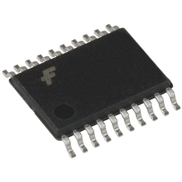
FMS6690MTC20X 是安森美(ON Semiconductor)推出的一款高性能、低功耗、单芯片三通道视频滤波驱动器,专为标清(SD)模拟视频信号处理设计。其典型应用场景包括:
- 消费类视频设备:如DVD播放器、机顶盒(STB)、AV接收器、电视调谐器模块等,用于对CVBS(复合视频)、S-Video(Y/C)或分量视频(YPbPr)信号进行重建滤波与缓冲驱动,提升图像清晰度并抑制高频噪声。
- 安防监控系统:在模拟摄像头后端(DVR/NVR视频输入接口)中,对多路模拟视频信号进行抗混叠滤波和75Ω阻抗匹配驱动,确保长线传输后的信号完整性与稳定性。
- 车载影音系统:适用于车载导航、倒车影像等需多路模拟视频输入的场景,满足AEC-Q100 Grade 2可靠性要求(该器件符合汽车级温度范围–40°C至+105°C),支持宽电压供电(2.7V–5.5V),具备低静态电流特性,适合嵌入式低功耗应用。
- 工业显示与视频采集卡:作为视频信号调理前端,集成3路独立6dB增益、8MHz(–3dB)巴特沃斯低通滤波器及轨到轨输出驱动器,可直接驱动双绞线或同轴电缆,简化PCB设计,无需外置滤波元件。

该芯片采用20引脚TSSOP封装(MTC20X),集成度高、外围精简,显著降低BOM成本与PCB面积,是替代传统分立滤波+放大方案的理想选择。
| 参数 | 数值 |
| 产品目录 | 集成电路 (IC) |
| 描述 | IC VIDEO FILTER DRVR 6CH 20TSSOP |
| 产品分类 | |
| 品牌 | Fairchild Semiconductor |
| 数据手册 | |
| 产品图片 |
|
| 产品型号 | FMS6690MTC20X |
| rohs | 无铅 / 符合限制有害物质指令(RoHS)规范要求 |
| 产品系列 | - |
| 产品目录页面 | |
| 供应商器件封装 | 20-TSSOP |
| 其它名称 | FMS6690MTC20XDKR |
| 包装 | Digi-Reel® |
| 安装类型 | 表面贴装 |
| 封装/外壳 | 20-TSSOP(0.173",4.40mm 宽) |
| 应用 | 录音机,机顶盒 |
| 标准包装 | 1 |
| 类型 | 视频滤波器 |
.jpg)


- 商务部:美国ITC正式对集成电路等产品启动337调查
- 曝三星4nm工艺存在良率问题 高通将骁龙8 Gen1或转产台积电
- 太阳诱电将投资9.5亿元在常州建新厂生产MLCC 预计2023年完工
- 英特尔发布欧洲新工厂建设计划 深化IDM 2.0 战略
- 台积电先进制程称霸业界 有大客户加持明年业绩稳了
- 达到5530亿美元!SIA预计今年全球半导体销售额将创下新高
- 英特尔拟将自动驾驶子公司Mobileye上市 估值或超500亿美元
- 三星加码芯片和SET,合并消费电子和移动部门,撤换高东真等 CEO
- 三星电子宣布重大人事变动 还合并消费电子和移动部门
- 海关总署:前11个月进口集成电路产品价值2.52万亿元 增长14.8%

-STD-PBS-R.jpg)


PDF Datasheet 数据手册内容提取
Is Now Part of To learn more about ON Semiconductor, please visit our website at www.onsemi.com Please note: As part of the Fairchild Semiconductor integration, some of the Fairchild orderable part numbers will need to change in order to meet ON Semiconductor’s system requirements. Since the ON Semiconductor product management systems do not have the ability to manage part nomenclature that utilizes an underscore (_), the underscore (_) in the Fairchild part numbers will be changed to a dash (-). This document may contain device numbers with an underscore (_). Please check the ON Semiconductor website to verify the updated device numbers. The most current and up-to-date ordering information can be found at www.onsemi.com. Please email any questions regarding the system integration to Fairchild_questions@onsemi.com. ON Semiconductor and the ON Semiconductor logo are trademarks of Semiconductor Components Industries, LLC dba ON Semiconductor or its subsidiaries in the United States and/or other countries. ON Semiconductor owns the rights to a number of patents, trademarks, copyrights, trade secrets, and other intellectual property. A listing of ON Semiconductor’s product/patent coverage may be accessed at www.onsemi.com/site/pdf/Patent-Marking.pdf. ON Semiconductor reserves the right to make changes without further notice to any products herein. ON Semiconductor makes no warranty, representation or guarantee regarding the suitability of its products for any particular purpose, nor does ON Semiconductor assume any liability arising out of the application or use of any product or circuit, and specifically disclaims any and all liability, including without limitation special, consequential or incidental damages. Buyer is responsible for its products and applications using ON Semiconductor products, including compliance with all laws, regulations and safety requirements or standards, regardless of any support or applications information provided by ON Semiconductor. “Typical” parameters which may be provided in ON Semiconductor data sheets and/or specifications can and do vary in different applications and actual performance may vary over time. All operating parameters, including “Typicals” must be validated for each customer application by customer’s technical experts. ON Semiconductor does not convey any license under its patent rights nor the rights of others. ON Semiconductor products are not designed, intended, or authorized for use as a critical component in life support systems or any FDA Class 3 medical devices or medical devices with a same or similar classification in a foreign jurisdiction or any devices intended for implantation in the human body. Should Buyer purchase or use ON Semiconductor products for any such unintended or unauthorized application, Buyer shall indemnify and hold ON Semiconductor and its officers, employees, subsidiaries, affiliates, and distributors harmless against all claims, costs, damages, and expenses, and reasonable attorney fees arising out of, directly or indirectly, any claim of personal injury or death associated with such unintended or unauthorized use, even if such claim alleges that ON Semiconductor was negligent regarding the design or manufacture of the part. ON Semiconductor is an Equal Opportunity/Affirmative Action Employer. This literature is subject to all applicable copyright laws and is not for resale in any manner.
F M S 6 6 August 2009 9 0 — S FMS6690 ix C Six Channel, 6th Order, SD/PS/HD Video Filter Driver h a n n e l , 6 Features Description th O (cid:131) Three Selectable Sixth-Order 15/32MHz (PS/HD) The FMS6690 Low-Cost Video Filter (LCVF) is intended r Filters to replace passive LC filters and drivers with a low-cost d integrated device. Six 6th-order Butterworth filters er (cid:131) Three Fixed Sixth-Order 8MHz (SD) Filters with provide improved image quality compared to typical , S MUXed Input passive solutions. The combination of low-power D (cid:131) Transparent Input Clamping Standard Definition (SD), Progressive Scan (PS), and /S High Definition (HD) filters greatly simplifies DVD video P (cid:131) Single Video Load Drive (2VPP, 150Ω, AV= 6dB) output circuitry. Three channels offer fixed SD filters /H (cid:131) AC-or DC-Coupled Inputs and feature an additional MUXed input, while the other D three channels are selectable between PS and HD V (cid:131) AC-or DC-Coupled Outputs filters. The FMS6690 offers a fixed gain of 6dB. i d (cid:131) DC-Coupled Outputs Eliminate AC-Coupling The FMS6690 may be directly driven by a DC-coupled eo Capacitors DAC output or an AC-coupled signal. Internal diode F (cid:131) Low Power clamps and bias circuitry may be used if AC-coupled ilt inputs are required (see Applications section for e (cid:131) 5V Only details). r D r The outputs can drive AC-or DC-coupled single (150Ω) i v Applications video loads. DC-coupling the outputs removes the need e r for output coupling capacitors. The input DC levels are (cid:131) Cable and Satellite Set-Top Boxes offset approximately +280mV at the output. (cid:131) DVD Players (cid:131) HDTV (cid:131) Personal Video Recorders (PVR) (cid:131) Video On Demand (VOD) Ordering Information Operating Eco Packing Part Number Temperature Package Status Method Range 2500 Units in FMS6690MTC20X 0° to 70°C RoHS 20-Lead Thin Shrink Outline Package (TSSOP) Tape and Reel For Fairchild’s definition of Eco Status, please visit: http://www.fairchildsemi.com/company/green/rohs_green.html. © 2006 Fairchild Semiconductor Corporation www.fairchildsemi.com FMS6690 • Rev. 1.0.3
F M Block Diagram S 6 6 9 0 — S i x C h a n n e l , 6 th O r d e r , S D / P S / H D V i d e o Figure 1. Block Diagram F i l t e r D r i v e r © 2006 Fairchild Semiconductor Corporation www.fairchildsemi.com FMS6690 • Rev. 1.0.3 2
F M Pin Configuration S 6 6 9 0 — S i x C h a n n e l , 6 th O r d e r , S D / P S / H D V id e Figure 2. Pin Configuration o F i l t Pin Definitions e r D Pin # Name Type Description r i v 1 SD IN1 Input SD Video Input, Channel 1 e r 2 SD IN2 Input SD Video Input, Channel 2 3 SD IN3A Input SD Video Input, Channel 3A 4 SD IN3B Input SD Video Input, Channel 3B 5 VCC Input +5V Supply 6 FcSEL Input Selects Filter Corner Rrequency for Pins 7, 8, and 9; “0” = PS, “1” = HD 7 PS/HD IN1 Input Selectable PS or HD Video Input, Channel 1 8 PS/HD IN2 Input Selectable PS or HD Video Input, Channel 2 9 PS/HD IN3 Input Selectable PS or HD Video Input, Channel 3 10 N/C Input No Connect 11 N/C Input No Connect 12 PS/HD OUT3 Output Filtered PS or HD Video Output, Channel 3 13 PS/HD OUT2 Output Filtered PS or HD Video Output, Channel 2 14 PS/HD OUT1 Output Filtered PS or HD Video Output, Channel 1 15 MUX Input MUX Selects Between Channel 3A and 3B Inputs; 0 = A, 1 = B SEL 16 GND Input Must Be Tied to Ground 17 GND Input Must Be Tied to Ground 18 SD OUT3 Output Filtered SD Video Output, Channel 3 19 SD OUT2 Output Filtered SD Video Output, Channel 2 20 SD OUT1 Output Filtered SD Video Output, Channel 1 © 2006 Fairchild Semiconductor Corporation www.fairchildsemi.com FMS6690 • Rev. 1.0.3 3
F M Absolute Maximum Ratings S 6 Stresses exceeding the absolute maximum ratings may damage the device. The device may not function or be 6 9 operable above the recommended operating conditions and stressing the parts to these levels is not recommended. 0 In addition, extended exposure to stresses above the recommended operating conditions may affect device — reliability. The absolute maximum ratings are stress ratings only. S i Symbol Parameter Min. Max. Unit x C VCC DC Supply Voltage -0.3 6.0 V h a V Analog Digital I/O -0.3 V + 0.3 V n IO CC n I Output Current, Any One Channel, Do Not Exceed 50 mA e OUT l , Electrostatic Discharge Human Body Model, JESD22-A114 9 6 ESD Capability Charged Device Model, JESD22-C101 2 kV th O r d e r , Reliability Information S D / Symbol Parameter Min. Typ. Max. Unit P S TJ Junction Temperature +150 °C /H D T Storage Temperature Range -65 +150 °C STG V TL Lead Temperature, Soldering 10 Seconds +300 °C id Thermal Resistance, JEDEC Standard, Multi-Layer Test Board, e Θ 74 °C/W o JA Still Air F il t e r D Recommended Operating Conditions r i v The Recommended Operating Conditions table defines the conditions for actual device operation. Recommended e r operating conditions are specified to ensure optimal performance to the datasheet specifications. Fairchild does not recommend exceeding them or designing to Absolute Maximum Ratings. Symbol Parameter Min. Typ. Max. Unit T Operating Temperature Range 0 +70 °C A V Supply Voltage Range 4.75 5.00 5.25 V CC DC Electrical Characteristics Unless otherwise noted, T =25°C, V =5V, AC coupled with 0.1µF, all outputs AC coupled with 220µF into 150Ω A CC loads, referenced to 400kHz. Symbol Parameter Conditions Min. Typ. Max. Units I Supply Current(1) No Load 60 80 mA CC V Video Input Voltage Range Referenced to GND if DC Coupled 1.4 V IN PP V Digital Input Low(1) F 0 0.8 V IL cSEL V Digital Input High(1) F 2.4 V V IH cSEL CC Note: 1. 100% tested at 25°C. © 2006 Fairchild Semiconductor Corporation www.fairchildsemi.com FMS6690 • Rev. 1.0.3 4
F Standard-Definition Electrical Characteristics M S Unless otherwise noted, T =25°C, V =1V , V =5V, all inputs AC coupled with 0.1µF, all outputs AC coupled with 6 A IN PP CC 6 220µF into 150Ω loads, referenced to 400kHz. 9 0 Symbol Parameter Conditions Min. Typ. Max. Units — AVSD Channel Gain(2) All SD Channels 5.6 6.0 6.4 dB S f -1dB Flatness(2) All SD Channels 5.20 7.15 MHz ix 1dBSD f -3dB Bandwidth(2) All SD Channels 6.5 8.0 MHz C cSD h f Attenuation (Stopband Reject)(2) All SD Channels at f=27MHz 43 50 dB a SBSD n DG Differential Gain All SD Channels 0.7 % n e DP Differential Phase All SD Channels 1.0 ° l, 6 THD Distortion, Output VOUT=1.4VPP, 3.58MHz 0.35 % th O X Crosstalk (Ch-to-Ch) at 1MHz -54 dB TALKSD r SNR Signal-to-Noise Ratio(3) NTC-7 Weighting, 100kHz to 4.2MHz 72 dB d e r tpdSD Propagation Delay Delay from Input to Output, 4.5MHz 90 ns , S Notes: D 2. 100% tested at 25°C. /P 3. SNR=20 • log (714mV / rms noise). S / H Progressive Scan Electrical Characteristics D V Unless otherwise noted, T =25°C, V =1V , V =3.3V, R =37.5Ω, all inputs AC coupled with 0.1µF, all outputs A IN PP CC SOURCE i d AC coupled with 220µF into 150Ω loads, referenced to 400kHz. e o Symbol Parameter Conditions Min. Typ. Max. Units F AV Channel Gain(4) All PS Channels 5.6 6.0 6.4 dB il PS t e f -1dB Flatness(4) All PS Channels 12 14 MHz r 1dBSD D fcPS -3dB Bandwidth(4) All PS Channels 13 16 MHz r i fSBSD Attenuation (Stopband Reject)(4) All PS Channels at f=54MHz 37 45 dB ve r Total Harmonic Distortion, THD V =1.4V , 7MHz 0.35 % Output (All PS Channels) OUT PP X Crosstalk (Ch-to-Ch) at 1MHz -53 dB TALKPS SNR Signal-to-Noise Ratio(5) Unweighted, 100kHz to 15MHz 66 dB t Propagation Delay Delay from Input to Output 47 ns pdSD Notes: 4. 100% tested at 25°C. 5. SNR=20 • log (714mV / rms noise). High-Definition Electrical Characteristics Unless otherwise noted, T =25°C, V =1V , V =5V, R =37.5Ω, all inputs AC coupled with 0.1µF, all outputs A IN PP CC SOURCE AC coupled with 220µF into 150Ω loads, referenced to 400kHz. Symbol Parameter Conditions Min. Typ. Max. Units AV Channel Gain(6) All HD Channels 5.6 6.0 6.4 dB HD f -1dB Flatness(6) All HD Channels 28 31 MHz 1dBHD f -3dB Bandwidth(6) All HD Channels 30 34 MHz cHD f Attenuation (Stopband Reject)(6) All HD Channels at f=74.25MHz 30 41 dB SBHD THD Output Distortion,(All PS Channels) V =1.4V , 22MHz 0.9 % OUT PP X Crosstalk (Ch-to-Ch) at 1MHz -54 dB TALKHD SNR Signal-to-Noise Ratio(7) Unweighted, 100kHz to 30MHz 60 dB t Propagation Delay Delay from Input to Output 25 ns pdHD Notes: 6. 100% tested at 25°C. 7. SNR=20 • log (714mV / rms noise). © 2006 Fairchild Semiconductor Corporation www.fairchildsemi.com FMS6690 • Rev. 1.0.3 5
F M Typical Performance Characteristics S 6 Unless otherwise noted T =25°C, V =1V , V =5V, R =37.5Ω, inputs AC coupled with 0.1µF, all outputs AC 6 C IN PP CC SOURCE 9 coupled with 220µF into150Ω loads. 0 — S i x C h a n n e l , 6 th O r d e r , S D / P Figure 3. SD Gain vs. Frequency Figure 4. SD Flatness vs. Frequency S /H D V i d e o F i l t e r D r i v e r Figure 5. PS Gain vs. Frequency Figure 6. PS Flatness vs. Frequency Figure 7. HD Gain vs. Frequency Figure 8. HD Flatness vs. Frequency © 2006 Fairchild Semiconductor Corporation www.fairchildsemi.com FMS6690 • Rev. 1.0.3 6
F M Typical Performance Characteristics S 6 Unless otherwise notedT =25°C, V =1V , V =5V, R =37.5Ω, inputs AC coupled with 0.1µF, all outputs AC 6 C IN PP CC SOURCE 9 coupled with 220µF into150Ω loads. 0 — S i x C h a n n e l , 6 th O r d e r , S D / P Figure 9. SD Group Delay vs. Frequency Figure 10. Noise vs. Frequency S /H D V i d e o F i l t e r D r i v e r Figure 11. PS Group Delay vs. Frequency Figure 12. SD Differential Gain Figure 13. HD Group Delay vs. Frequency © 2006 Fairchild Semiconductor Corporation www.fairchildsemi.com FMS6690 • Rev. 1.0.3 7
F M Applications Information S 6 Functional Description 6 9 The FMS6690 Low-Cost Video Filter (LCVF) provides 0 6dB gain (9dB optional, contact factory for further — information) from input to output. In addition, the input is 0.65V S slightly offset to optimize the output driver performance. i The offset is held to the minimum required value to x C decrease the standing DC current into the load. Typical h voltage levels are shown in Figure 14. YIN Driver a YOUT n n e 800kΩ l, 6 th Figure 15. Input Clamp Circuit O r d I/O Configurations e r , For DC-coupled DAC drive with DC-coupled outputs, S use the configuration in Figure 16. D / P S / 0V - 1.4V H DVD or LCVF 75Ω D STB Clamp V SoC Inactive i DAC d e Output o F i l t e r Figure 16. DC-Coupled Inputs and Outputs D r Alternatively, if the DAC’s average DC output level i v causes the signal to exceed the range of 0V to 1.4V, it e r can be AC-coupled, as shown in Figure 17. 0V - 1.4V DVD or 0.1µ LCVF 75Ω STB Clamp SoC Active DAC Output Figure 14. Typical Voltage Levels The FMS6690 provides an internal diode clamp to support AC-coupled input signals. If the input signal does not go below ground, the input clamp does not Figure 17. AC-Coupled Inputs, DC-coupled Outputs operate. This allows DAC outputs to directly drive the When the FMS6690 is driven by an unknown external FMS6690 without an AC coupling capacitor. The worst- source or a SCART with its own clamping circuitry, the case sync tip compression, due to the clamp, does not inputs should be AC-coupled, shown in Figure 18. exceed 7mV. The input level set by the clamp, combined with the internal DC offset, keeps the output within acceptable range. When the input is AC-coupled, 0V - 1.4V the diode clamp sets the sync tip (or lowest voltage) just 0.1µ LCVF 75Ω External Video below ground. Clamp source must Active be AC-coupled. For symmetric signals like C, U, V, Cb, Cr, Pb, and Pr; 75Ω the average DC bias is fairly constant and the inputs can be AC-coupled with the addition of a pull-up resistor to set the DC input voltage. DAC outputs can also drive these same signals without the AC coupling capacitor. A conceptual illustration of the input clamp circuit is Figure 18. SCART with DC-Coupled Outputs shown in Figure 15. © 2006 Fairchild Semiconductor Corporation www.fairchildsemi.com FMS6690 • Rev. 1.0.3 8
F M The same method can be used for biased signals with S T= T + P • Θ (1) the addition of a pull-up resistor to make sure the clamp J A d JA 6 6 never operates. The internal pull-down resistance is where Pd= PCH1+ PCH2+ PCHx, 9 800kΩ ±20%, so the external resistance should be and PCHx= VS • ICH- (VO2/RL) (2) 0 — 7.5MΩ to set the DC level to 500mV. If a pull-up resistance of less than 7.5MΩ desired, add an external where: S V = 2V + 0.280V; pull-down such that the DC input level is set to 500mV. I O= (I IN/ 6) + (V /R ); ix CH CC O L V = RMS value of input signal; C IN h ICC = 60mA; a External Video V = 5V; and n S source must 7.5MΩ R = channel load resistance. n be AC-coupled. 0.1µ LCVF 75Ω L e Bias Board layout affects thermal characteristics. Refer to l, Input 6 the Layout Considerations section for more information. th 75Ω 500mV +/-350mV O Output Considerations r d The FMS6690 outputs are DC offset from the input by e r Figure 19. Biased SCART with DC-Coupled Outputs 150mV therefore, VOUT = 2•VIN DC+150mv. This offset , S is required to obtain optimal performance from the D The same circuits can be used with AC-coupled outputs output driver and is held at the minimum value to / P if desired. decrease the standing DC current into the load. Since S the FMS6690 has a 2x (6dB) gain, the output is typically / H connected via a 75Ω-series back-matching resistor D 0V - 1.4V followed by the 75Ω video cable. Because of the DVD or LCVF 75Ω 220µ V STB Clamp inherent divide by two of this configuration, the blanking id SoC Inactive level at the load of the video signal is always less then e DAC 1V. When AC-coupling the output, ensure that the o Output coupling capacitor of choice passes the lowest F i frequency content in the video signal and that line time lt e distortion (video tilt) is kept as low as possible. r D Figure 20. DC-Coupled Inputs, AC-coupled Outputs The selection of the coupling capacitor is a function of r the subsequent circuit input impedance and the leakage iv current of the input being driven. To obtain the highest- e External video r source must 7.5MΩ quality output video signal, the series termination be AC-coupled. 0.1µ LCVF 75Ω 220µ resistor must be placed as close to the device output Clamp Active pin as possible. This greatly reduces the parasitic capacitance and inductance effect on the FMS6690 75Ω 500mV +/-350mV output driver. The distance from device pin to place series termination resistor should be no greater than 0.1 inches. Figure 21. Biased SCART with AC-Coupled Outputs Note: 8. The video tilt or line time distortion is dominated by the AC-coupling capacitor. The value may need to be increased beyond 220µF to obtain satisfactory operation in some applications. Power Dissipation The FMS6690 output drive configuration must be considered when calculating overall power dissipation. Care must be taken not to exceed the maximum die junction temperature. The following example can be used to calculate the FMS6690’s power dissipation and Figure 22. Distance from Device Pin to Series internal temperature rise. Termination Resistor © 2006 Fairchild Semiconductor Corporation www.fairchildsemi.com FMS6690 • Rev. 1.0.3 9
F M S Layout Considerations 6 6 Layout and supply bypassing play major roles in high- (cid:131) Include 10µF and 0.1μF ceramic bypass 90 frequency performance and thermal characteristics. capacitors. — Fairchild offers a demonstration board, FMS6690DEMO, to use as a guide for layout and to aid (cid:131) Place the 10μF capacitor within 0.75 inches of the S in device testing and characterization. The power pin. ix FMS6690DEMO is a four-layer board with a full power (cid:131) Place the 0.1μF capacitor within 0.1 inches of the C and ground plane. Following this layout configuration h power pin. a provides the optimum performance and thermal characteristics. For optimum results, follow these steps (cid:131) For multi-layer boards, use a large ground plane to nn as a basis for high-frequency layout: help dissipate heat. e l , (cid:131) For 2 layer boards, use a ground plane that 6 extends beyond the device by at least 0.5. th O (cid:131) Minimize all trace lengths to reduce series r d inductances. e r , S D / P S / H D V i d e o F i l t e r D r i v e r © 2006 Fairchild Semiconductor Corporation www.fairchildsemi.com FMS6690 • Rev. 1.0.3 10
F M Typical Application S 6 6 9 0 — S i x C h a n n e l , 6 th O r d e r , S D / P S / H D V i d e o F i l t e r D r i v e r Figure 23. Typical Application Diagram © 2006 Fairchild Semiconductor Corporation www.fairchildsemi.com FMS6690 • Rev. 1.0.3 11
F M Physical Dimensions S 6 6 9 0 — S i x C h a n n e l , 6 th O r d e r , S D / P S / H D V i d e o F i l t e r D r i v e r Figure 24. 20-Lead Thin Shrink Outline Package (TSSOP) Package drawings are provided as a service to customers considering Fairchild components. Drawings may change in any manner without notice. Please note the revision and/or date on the drawing and contact a Fairchild Semiconductor representative to verify or obtain the most recent revision. Package specifications do not expand the terms of Fairchild’s worldwide terms and conditions, specifically the warranty therein, which covers Fairchild products. Always visit Fairchild Semiconductor’s online packaging area for the most recent package drawings: http://www.fairchildsemi.com/packaging/. © 2006 Fairchild Semiconductor Corporation www.fairchildsemi.com FMS6690 • Rev. 1.0.3 12
F M S 6 6 9 0 — S i x C h a n n e l , 6 th O r d e r , S D / P S / H D V i d e o F i l t e r D r i v e r © 2006 Fairchild Semiconductor Corporation www.fairchildsemi.com FMS6690 • Rev. 1.0.3 13
ON Semiconductor and are trademarks of Semiconductor Components Industries, LLC dba ON Semiconductor or its subsidiaries in the United States and/or other countries. ON Semiconductor owns the rights to a number of patents, trademarks, copyrights, trade secrets, and other intellectual property. A listing of ON Semiconductor’s product/patent coverage may be accessed at www.onsemi.com/site/pdf/Patent−Marking.pdf. ON Semiconductor reserves the right to make changes without further notice to any products herein. ON Semiconductor makes no warranty, representation or guarantee regarding the suitability of its products for any particular purpose, nor does ON Semiconductor assume any liability arising out of the application or use of any product or circuit, and specifically disclaims any and all liability, including without limitation special, consequential or incidental damages. Buyer is responsible for its products and applications using ON Semiconductor products, including compliance with all laws, regulations and safety requirements or standards, regardless of any support or applications information provided by ON Semiconductor. “Typical” parameters which may be provided in ON Semiconductor data sheets and/or specifications can and do vary in different applications and actual performance may vary over time. All operating parameters, including “Typicals” must be validated for each customer application by customer’s technical experts. ON Semiconductor does not convey any license under its patent rights nor the rights of others. ON Semiconductor products are not designed, intended, or authorized for use as a critical component in life support systems or any FDA Class 3 medical devices or medical devices with a same or similar classification in a foreign jurisdiction or any devices intended for implantation in the human body. Should Buyer purchase or use ON Semiconductor products for any such unintended or unauthorized application, Buyer shall indemnify and hold ON Semiconductor and its officers, employees, subsidiaries, affiliates, and distributors harmless against all claims, costs, damages, and expenses, and reasonable attorney fees arising out of, directly or indirectly, any claim of personal injury or death associated with such unintended or unauthorized use, even if such claim alleges that ON Semiconductor was negligent regarding the design or manufacture of the part. ON Semiconductor is an Equal Opportunity/Affirmative Action Employer. This literature is subject to all applicable copyright laws and is not for resale in any manner. PUBLICATION ORDERING INFORMATION LITERATURE FULFILLMENT: N. American Technical Support: 800−282−9855 Toll Free ON Semiconductor Website: www.onsemi.com Literature Distribution Center for ON Semiconductor USA/Canada 19521 E. 32nd Pkwy, Aurora, Colorado 80011 USA Europe, Middle East and Africa Technical Support: Order Literature: http://www.onsemi.com/orderlit Phone: 303−675−2175 or 800−344−3860 Toll Free USA/Canada Phone: 421 33 790 2910 Fax: 303−675−2176 or 800−344−3867 Toll Free USA/Canada Japan Customer Focus Center For additional information, please contact your local Email: orderlit@onsemi.com Phone: 81−3−5817−1050 Sales Representative © Semiconductor Components Industries, LLC www.onsemi.com www.onsemi.com 1
Mouser Electronics Authorized Distributor Click to View Pricing, Inventory, Delivery & Lifecycle Information: O N Semiconductor: FMS6690MTC20X