 Datasheet下载
- 型号: FMS6151L6X_F085
- 制造商: Fairchild Semiconductor
- 库位|库存: xxxx|xxxx
- 要求:
| 数量阶梯 | 香港交货 | 国内含税 |
| +xxxx | $xxxx | ¥xxxx |
查看当月历史价格
查看今年历史价格
FMS6151L6X_F085产品简介:
ICGOO电子元器件商城为您提供FMS6151L6X_F085由Fairchild Semiconductor设计生产,在icgoo商城现货销售,并且可以通过原厂、代理商等渠道进行代购。 FMS6151L6X_F085价格参考。Fairchild SemiconductorFMS6151L6X_F085封装/规格:线性 - 视频处理, 。您可以下载FMS6151L6X_F085参考资料、Datasheet数据手册功能说明书,资料中有FMS6151L6X_F085 详细功能的应用电路图电压和使用方法及教程。
ON Semiconductor(安森美半导体)的FMS6151L6X_F085是一款属于线性 - 视频处理类别的集成电路。该型号主要应用于视频信号处理领域,具体应用场景包括:

1. 视频监控系统:FMS6151L6X_F085可用于摄像机中的视频信号处理,支持高质量的图像传输和优化,确保视频监控系统的清晰度和稳定性。

2. 汽车电子:在车载摄像头系统中,该芯片可以处理来自倒车摄像头或环视系统的视频信号,提供低延迟、高分辨率的图像输出,增强驾驶安全性。

3. 工业自动化:用于工业视觉系统中,如机器视觉设备,能够处理复杂的视频数据流,提高生产线检测效率和精度。

4. 消费电子产品:适用于数字摄像机、网络摄像头等设备,提供高效的视频信号转换和处理功能,改善用户体验。

5. 医疗成像:在医疗设备中,如内窥镜或超声波成像系统,这款芯片可实现对高精度图像的实时处理,帮助医生进行准确诊断。

FMS6151L6X_F085以其卓越的性能和可靠性,为上述应用提供了稳定的视频信号处理解决方案,满足不同行业对高质量视频处理的需求。
| 参数 | 数值 |
| 产品目录 | 集成电路 (IC) |
| 描述 | IC FILTER LCVF 6MICROPAK |
| 产品分类 | |
| 品牌 | Fairchild Semiconductor |
| 数据手册 | |
| 产品图片 | |
| 产品型号 | FMS6151L6X_F085 |
| rohs | 无铅 / 符合限制有害物质指令(RoHS)规范要求 |
| 产品系列 | - |
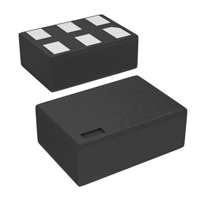
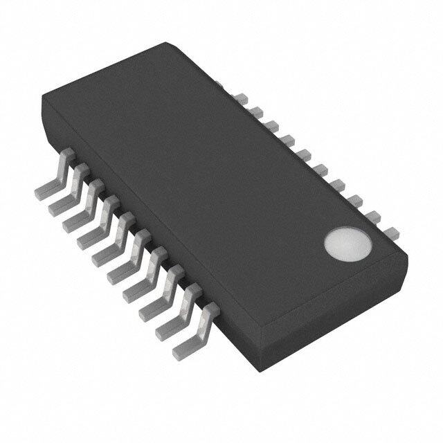
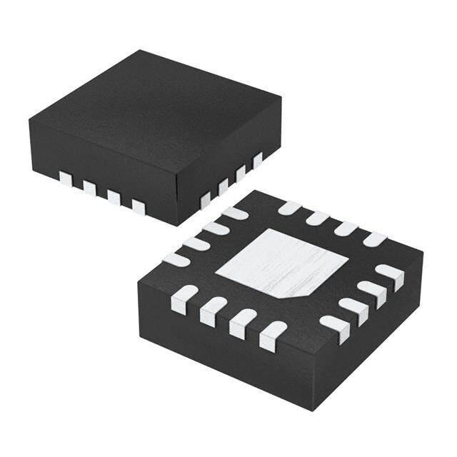
| 供应商器件封装 | 6-MicroPak |
| 其它名称 | FMS6151L6X_F085DKR |
| 包装 | Digi-Reel® |
| 安装类型 | 表面贴装 |
| 封装/外壳 | 6-UFDFN |
| 应用 | 数码相机,PDA,机顶盒 |
| 标准包装 | 1 |
| 类型 | 视频滤波器 |


- 商务部:美国ITC正式对集成电路等产品启动337调查
- 曝三星4nm工艺存在良率问题 高通将骁龙8 Gen1或转产台积电
- 太阳诱电将投资9.5亿元在常州建新厂生产MLCC 预计2023年完工
- 英特尔发布欧洲新工厂建设计划 深化IDM 2.0 战略
- 台积电先进制程称霸业界 有大客户加持明年业绩稳了
- 达到5530亿美元!SIA预计今年全球半导体销售额将创下新高
- 英特尔拟将自动驾驶子公司Mobileye上市 估值或超500亿美元
- 三星加码芯片和SET,合并消费电子和移动部门,撤换高东真等 CEO
- 三星电子宣布重大人事变动 还合并消费电子和移动部门
- 海关总署:前11个月进口集成电路产品价值2.52万亿元 增长14.8%


PDF Datasheet 数据手册内容提取
Is Now Part of To learn more about ON Semiconductor, please visit our website at www.onsemi.com Please note: As part of the Fairchild Semiconductor integration, some of the Fairchild orderable part numbers will need to change in order to meet ON Semiconductor’s system requirements. Since the ON Semiconductor product management systems do not have the ability to manage part nomenclature that utilizes an underscore (_), the underscore (_) in the Fairchild part numbers will be changed to a dash (-). This document may contain device numbers with an underscore (_). Please check the ON Semiconductor website to verify the updated device numbers. The most current and up-to-date ordering information can be found at www.onsemi.com. Please email any questions regarding the system integration to Fairchild_questions@onsemi.com. ON Semiconductor and the ON Semiconductor logo are trademarks of Semiconductor Components Industries, LLC dba ON Semiconductor or its subsidiaries in the United States and/or other countries. ON Semiconductor owns the rights to a number of patents, trademarks, copyrights, trade secrets, and other intellectual property. A listing of ON Semiconductor’s product/patent coverage may be accessed at www.onsemi.com/site/pdf/Patent-Marking.pdf. ON Semiconductor reserves the right to make changes without further notice to any products herein. ON Semiconductor makes no warranty, representation or guarantee regarding the suitability of its products for any particular purpose, nor does ON Semiconductor assume any liability arising out of the application or use of any product or circuit, and specifically disclaims any and all liability, including without limitation special, consequential or incidental damages. Buyer is responsible for its products and applications using ON Semiconductor products, including compliance with all laws, regulations and safety requirements or standards, regardless of any support or applications information provided by ON Semiconductor. “Typical” parameters which may be provided in ON Semiconductor data sheets and/or specifications can and do vary in different applications and actual performance may vary over time. All operating parameters, including “Typicals” must be validated for each customer application by customer’s technical experts. ON Semiconductor does not convey any license under its patent rights nor the rights of others. ON Semiconductor products are not designed, intended, or authorized for use as a critical component in life support systems or any FDA Class 3 medical devices or medical devices with a same or similar classification in a foreign jurisdiction or any devices intended for implantation in the human body. Should Buyer purchase or use ON Semiconductor products for any such unintended or unauthorized application, Buyer shall indemnify and hold ON Semiconductor and its officers, employees, subsidiaries, affiliates, and distributors harmless against all claims, costs, damages, and expenses, and reasonable attorney fees arising out of, directly or indirectly, any claim of personal injury or death associated with such unintended or unauthorized use, even if such claim alleges that ON Semiconductor was negligent regarding the design or manufacture of the part. ON Semiconductor is an Equal Opportunity/Affirmative Action Employer. This literature is subject to all applicable copyright laws and is not for resale in any manner.
F M S 6 1 June 2010 5 1 FMS6151 — U Ultra-Portable Video Filter Driver l t r a - Features Description P o ■ 5th-Order 8MHz (SD) Filter r The FMS6151 low-cost integrated video fi lter is intended t a ■ Power Down to 25nA to replace passive LC fi lters and drivers in low-voltage b l ■ DC-Coupled Input portable video applications. The 5th-order fi lter provides e V ■ AC- or DC-Coupled Output better image quality compared to typical 2nd- and 3rd- i d ■ DC-Coupled Output Eliminates AC-Coupling Cap order passive solutions. e o ■ SAG Correction Reduces Size of AC-Coupling Cap The FMS6151 is intended to be directly driven by a DC- F ■ Fixed Gain of 6dB coupled DAC output. The output can drive an AC- or DC- il t ■ Small, Lead-Free, MicroPak™ Packaging coupled doubly terminated coax (150Ω) load. DC-coupling er the output removes the need for an expensive output D Applications r coupling capacitor. If an AC-cou pled output is needed, the iv ■ Digital Still Cameras e SAG correction circuit can be used to reduce the AC out- r ■ Camera Phones put coupling capacitor value. Input DC levels are offset by ■ Personal Digital Assistants approximately 100mV. This internal level shift is incorpo- ■ Set Top Boxes rated to prevent sync pulse clipping. ■ Digital Video Recorders Offering SAG correction, 6dB fi xed gain, and a 5th-order low-pass fi lter in a space-saving MicroPak™ package makes the FMS6151 well suited for space-sensitive appli- cations, such as cellular phones and digital cameras. Block Diagram V = 2.5V to 3.6V cc EN VIN + 8MHz, VO UT 5th order - SAG Figure 1. Block Diagram Ordering Information Part Number Operating Temperature Range Package Packaging Method FMS6151L6X -40°C to +105°C 6-Lead MicroPak™ Reel © 2006 Fairchild Semiconductor Corporation www.fairchildsemi.com FMS6151 • Rev. 1.0.6
F M Pin Confi guration S 6 1 5 1 — VIN 1 6 EN U l FMS6151 tr a - GND 2 5 Vcc P o r t a b l SAG 3 4 VOUT e V i d e o F i l t e Figure 2. Pin Assignments r D r i v e r Pin Assignments Pin# Pin Name Type Description 1 V Input Input video IN 2 GND Input Ground 3 SAG Input SAG 4 V Output Filtered video output OUT 5 V Input Positive power supply CC 6 EN Input Enable 0 = Disabled 1 = Enabled © 2006 Fairchild Semiconductor Corporation www.fairchildsemi.com FMS6151 • Rev. 1.0.6 2
F M Absolute Maximum Ratings S 6 Stresses exceeding the absolute maximum ratings may damage the device. The device may not function or be operable 1 5 above the recommended operating conditions and stressing the parts to these levels is not recommended. In addition, 1 extended exposure to stresses above the recommended operating conditions may affect device reliability. The absolute — maximum ratings are stress ratings only. U l t r Parameter Min. Max. Unit a - P DC Supply Voltage -0.3 6.0 V o Analog and Digital I/O -0.3 +VCC +0.3 V rta Maximum Output Current, Do Not Exceed 45 mA b l e Electrostatic Discharge Human Body Model, JESD22-A114 6 kV V Protection Level Charged Device Model, JESD22-C101 2 id e o F i l t e r Reliability Information D r i Parameter Min. Typ. Max. Unit v e r Junction Temperature +150 °C Storage Temperature Range -65 +150 °C Thermal Resistance (θ ), JDEC Standard, Multi-layer JA 271 °C/W Test Boards, Still Air Recommended Operating Conditions The Recommended Operating Conditions table defi nes the conditions for actual device operation. Recommended operating conditions are specifi ed to ensure optimal performance to the datasheet specifi cations. Fairchild does not recommend exceeding them or designing to absolute maximum ratings. Parameter Min. Typ. Max. Unit Operating Temperature Range -40 +105 °C Supply Voltage Range 2.5 2.7 3.6 V © 2006 Fairchild Semiconductor Corporation www.fairchildsemi.com FMS6151 • Rev. 1.0.6 3
F M DC Electrical Characteristics S 6 TA = 25°C, VCC = 2.7V, Rs = 37.5Ω, AC-coupled output into 150Ω load, SAG pin connected to VOUT pin, 1 5 unless otherwise noted. 1 — Symbol Parameter Conditions Min. Typ. Max. Units U ICC Supply Current(1) VCC = 2.7V, No Load 3.8 6.4 mA ltr a VIN Video Input Voltage Range Referenced to GND 1.2 Vpp -P Vols Output Level Shift(1) V = 0V 50 200 350 mV o IN r PSRR Vols over power supply VCC = 2.7V to 3.3V 40 dB ta b I Shut Down Current 25 nA l SH e V Disabled Logic Low(1) 0 0.8 V V il i V Enabled Logic High(1) V *0.6 V V d ih CC CC e t Enable Time 1.5 μs o ON F t Disable Time 50 ns i OFF lt e r D AC Electrical Characteristics r i v TA = 25°C, VCC = 2.7V, Rs = 37.5Ω, AC-coupled output into 150Ω load, SAG pin connected to VOUT pin, er unless otherwise noted. Symbol Parameter Conditions Min. Typ. Max. Units A Gain(1) DC 6.0 6.2 6.4 dB V f -1dB Bandwidth(1) 5.0 6.7 MHz 1dB f -3dB Bandwidth 8 MHz c f Attenuation(1) (Stopband Reject) 27MHz 40 47 dB SB DG Differential Gain 0.5 % DP Differential Phase 0.5 ° SNR Signal-to-Noise Ratio NTC-7 Weighting, 100kHz to 4.2MHz 78 dB Note: 1.100% tested at 25°C. © 2006 Fairchild Semiconductor Corporation www.fairchildsemi.com FMS6151 • Rev. 1.0.6 4
F M Typical Performance Characteristics S 6 TA = 25°C, VCC = 2.7V, Rs = 37.5Ω, AC-coupled output into 150Ω load, SAG pin connected to VOUT pin, 1 5 unless otherwise noted. 1 — 10 2.0 U 5 0 1 1.8 ltr 2 a -5 %) 1.6 -P Gain (dB)----11220505 MRekfr 4Fr0e0qkuHenzc y 6GdaiBn ain Error ( 11..42 ortabl G e -30 1 6.7MHz -1dB BW 1.0 V -35 23 82.70MMHHzz --34d2BdB BW 3 0.8 id -40 e -45 fSBSD = Gain(ref) – Gain(3) = 48dB 0.6 o F 0 5 10 15 20 25 30 -40 -30 -20 -10 0 10 20 30 40 50 60 70 80 i l Frequency (MHz) Temperature (°C) t e r Figure 3. Frequency Response Figure 4. Gain Error vs. Temperature D r i v e r 3.0 2.5 NTSC 2.0 without SAG Enable Pulse mplitude (V)21..00 al Gain (%) 110...5005 Signal A 0 Output Differenti---011...505 Min = -0.58 Max = 0.00 -2.0 ppMax = 0.58 -1.0 -2.5 -1 0 1 2 3 4 5 6 1st 2nd 3rd 4th 5th 6th Time (µs) Figure 5. Enable/Disable Response Figure 6. Differential Gain 7.0 2.5 NTSC 2.0 without SAG 6.0 eg) 1.5 d 5.0 e ( 1.0 I (mA)cc43..00 ntial Phas-00..055 2.0 ere-1.0 1.0 Diff-1.5 MMianx = = - 00..1528 -2.0 ppMax = 0.70 0 -2.5 2.5 3.0 3.5 4.0 4.5 5.0 5.5 1st 2nd 3rd 4th 5th 6th Vcc (V) Figure 7. I vs. Supply Voltage Figure 8. Differential Phase CC © 2006 Fairchild Semiconductor Corporation www.fairchildsemi.com FMS6151 • Rev. 1.0.6 5
F M Typical Performance Characteristics S 6 TA = 25°C, VCC = 2.7V, Rs = 37.5Ω, AC-coupled output into 150Ω load, SAG pin connected to VOUT pin, 1 5 unless otherwise noted. 1 — 4.0 60 U l 3.9 50 tra - P 40 A)3.8 A) o I (mcc3.7 I (nSH 30 rtabl 20 e V 3.6 10 id e o 3.5 0 F -40 -20 0 20 40 60 80 -40 -20 0 20 40 60 80 i l Temperature (°C) Temperature (°C) te r Figure 9. Supply Current vs. Temperature Figure 10. Shutdown Current vs. Temperature D r i v e r © 2006 Fairchild Semiconductor Corporation www.fairchildsemi.com FMS6151 • Rev. 1.0.6 6
F M Application Information SAG Correction S 6 SAG correction provides excellent performance with a 1 Input Voltage 5 small output coupling capacitor. It eliminates the 220μF - 1 The FMS6151 is intended to be directly driven by a DC- 1000μF output cou pling capacitors traditionally used. The — coupled DAC output. The input common-mode range of traditional output circuit (220μF into 150Ω load) creates a U the FMS6151 is 1.2Vpp, ground referenced. single pole (-3dB) at 5Hz. Reducing this capacitor causes lt r excessive phase shift, resulting in video fi eld tilt that can a Enable/Shutdown - P prevent proper recovery of the syn chronization signals. The FMS6151 has a shutdown feature that disables the o r output and reduces the quiescent current to ~25nA. This The FMS6151 SAG correction circuit provides a small ta feature is especially useful in portable applications, such amount of peaking, which provides compensation of the b l as cellular phones, hand held gaming devices, and video phase response, signifi cantly reducing video fi eld tilt. The e V cameras requiring video fi ltering and drive capability. SAG correction circuit allows decrease of the large 220μF i d output coupling capacitor. A 22μF is used for SAG correc- e Internal Level Shift tion and a 47μF is used for the outp ut coupling o F The FMS6151 has an internal level-shift circuit to avoid capacitor; much smaller and cheaper than traditional circuit i l t sync tip clipping. The output signal is shifted 200mV requirements. e r toward the VCC rail to help prevent clipping. This offset Output Confi guration D is useful when DC coupled out or using SAG correction. ri v The FMS6151 output is a low-impedance voltage driver. e It is capable of driving an AC- or DC-coupled single load. r For more application information, please refer to FMS6151 Application Note, AN-8005. © 2006 Fairchild Semiconductor Corporation www.fairchildsemi.com FMS6151 • Rev. 1.0.6 7
F M Physical Dimensions S 6 1 2X 5 1 0.05 C 1.45 B — 2X (1) U 0.05 C l t r a - P o (0.254) 1.00 (0.49) rt 5X a b (0.75) le V i d (0.52) e TOP VIEW A 1X o PIN 1 IDENTIFIER F 5 i l 0.55MAX (0.30) te PIN 1 6X r D 0.05 C r i v 0.05 RECOMMENED e 0.00 r LAND PATTERN 0.05 C C 0.45 0.106X 0.35 0.25 0.00 6X 0.15 DETAIL A 1.0 0.10 C B A 0.05 C 0.40 0.30 0.35 5X 0.25 0.40 5X 0.30 DETAIL A 0.075 X 45 PIN 1 TERMINAL 0.5 CHAMFER (0.05) (0.13) 6X 4X BOTTOM VIEW Notes: 1. CONFORMS TO JEDEC STANDARD M0-252 VARIATION UAAD 2. DIMENSIONS ARE IN MILLIMETERS 3. DRAWING CONFORMS TO ASME Y14.5M-1994 4. FILENAME AND REVISION: MAC06AREV4 5. PIN ONE IDENTIFIER IS 2X LENGTH OF ANY OTHER LINE IN THE MARK CODE LAYOUT. Figure 11. 6-Lead MicroPak™ Package Package drawings are provided as a service to customers considering Fairchild components. Drawings may change in any manner without notice. Please note the revision and/or date on the drawing and contact a Fairchild Semiconductor representative to verify or obtain the most recent revision. Package specifi cations do not expand the terms of Fairchild’s worldwide terms and conditions, specifi cally the warranty therein, which covers Fairchild products. Always visit Fairchild Semiconductor’s online packaging area for the most recent package drawings: http://www.fairchildsemi.com/packaging/. © 2006 Fairchild Semiconductor Corporation www.fairchildsemi.com FMS6151 • Rev. 1.0.6 8
F M S 6 1 5 1 — U l t r a - P o r t a b l e V i d e o F i l t e r D r i v e r © 2006 Fairchild Semiconductor Corporation www.fairchildsemi.com FMS6151 Rev. 1.0.6 9
ON Semiconductor and are trademarks of Semiconductor Components Industries, LLC dba ON Semiconductor or its subsidiaries in the United States and/or other countries. ON Semiconductor owns the rights to a number of patents, trademarks, copyrights, trade secrets, and other intellectual property. A listing of ON Semiconductor’s product/patent coverage may be accessed at www.onsemi.com/site/pdf/Patent−Marking.pdf. ON Semiconductor reserves the right to make changes without further notice to any products herein. ON Semiconductor makes no warranty, representation or guarantee regarding the suitability of its products for any particular purpose, nor does ON Semiconductor assume any liability arising out of the application or use of any product or circuit, and specifically disclaims any and all liability, including without limitation special, consequential or incidental damages. Buyer is responsible for its products and applications using ON Semiconductor products, including compliance with all laws, regulations and safety requirements or standards, regardless of any support or applications information provided by ON Semiconductor. “Typical” parameters which may be provided in ON Semiconductor data sheets and/or specifications can and do vary in different applications and actual performance may vary over time. All operating parameters, including “Typicals” must be validated for each customer application by customer’s technical experts. ON Semiconductor does not convey any license under its patent rights nor the rights of others. ON Semiconductor products are not designed, intended, or authorized for use as a critical component in life support systems or any FDA Class 3 medical devices or medical devices with a same or similar classification in a foreign jurisdiction or any devices intended for implantation in the human body. Should Buyer purchase or use ON Semiconductor products for any such unintended or unauthorized application, Buyer shall indemnify and hold ON Semiconductor and its officers, employees, subsidiaries, affiliates, and distributors harmless against all claims, costs, damages, and expenses, and reasonable attorney fees arising out of, directly or indirectly, any claim of personal injury or death associated with such unintended or unauthorized use, even if such claim alleges that ON Semiconductor was negligent regarding the design or manufacture of the part. ON Semiconductor is an Equal Opportunity/Affirmative Action Employer. This literature is subject to all applicable copyright laws and is not for resale in any manner. PUBLICATION ORDERING INFORMATION LITERATURE FULFILLMENT: N. American Technical Support: 800−282−9855 Toll Free ON Semiconductor Website: www.onsemi.com Literature Distribution Center for ON Semiconductor USA/Canada 19521 E. 32nd Pkwy, Aurora, Colorado 80011 USA Europe, Middle East and Africa Technical Support: Order Literature: http://www.onsemi.com/orderlit Phone: 303−675−2175 or 800−344−3860 Toll Free USA/Canada Phone: 421 33 790 2910 Fax: 303−675−2176 or 800−344−3867 Toll Free USA/Canada Japan Customer Focus Center For additional information, please contact your local Email: orderlit@onsemi.com Phone: 81−3−5817−1050 Sales Representative © Semiconductor Components Industries, LLC www.onsemi.com www.onsemi.com 1