ICGOO在线商城 > 集成电路(IC) > 接口 - 串行器,解串行器 > FIN212ACMLX

 Datasheet下载
- 型号: FIN212ACMLX
- 制造商: Fairchild Semiconductor
- 库位|库存: xxxx|xxxx
- 要求:
| 数量阶梯 | 香港交货 | 国内含税 |
| +xxxx | $xxxx | ¥xxxx |
查看当月历史价格
查看今年历史价格
FIN212ACMLX产品简介:
ICGOO电子元器件商城为您提供FIN212ACMLX由Fairchild Semiconductor设计生产,在icgoo商城现货销售,并且可以通过原厂、代理商等渠道进行代购。 FIN212ACMLX价格参考¥6.91-¥7.22。Fairchild SemiconductorFIN212ACMLX封装/规格:接口 - 串行器,解串行器, Serializer/Deserializer 12/2 Input 2/12 Output 32-MLP (5x5)。您可以下载FIN212ACMLX参考资料、Datasheet数据手册功能说明书,资料中有FIN212ACMLX 详细功能的应用电路图电压和使用方法及教程。
ON Semiconductor的FIN212ACMLX是一款串行器/解串行器(SerDes)芯片,属于其接口产品系列。该器件主要用于实现并行数据与串行数据之间的转换,适用于需要高速数据传输的应用场景。

主要应用场景包括:

1. 工业自动化系统:在工业控制和自动化设备中,用于高速数据采集与传输,提升系统响应速度与稳定性。

2. 视频与图像传输:适用于视频采集与显示系统,如安防监控、医疗成像设备等,支持高清视频信号的串行化传输。

3. 通信设备:用于通信基础设施中,如基站、光模块等,实现数据的高速点对点传输。

4. 汽车电子:在车载信息娱乐系统、摄像头模块与主控单元之间进行高速数据传输。

5. 测试与测量设备:用于高速信号分析仪、示波器等测试设备中,实现高精度数据采集与处理。

该芯片采用低电压差分信号(LVDS)技术,具有低功耗、高抗干扰能力和高传输速率的优点,适合在复杂电磁环境中稳定工作。其紧凑的封装形式(如TSSOP)也有利于在空间受限的应用中使用。
| 参数 | 数值 |
| 产品目录 | 集成电路 (IC)半导体 |
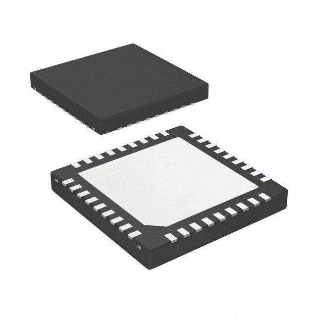
| 描述 | IC SERIAL/DESERIAL 12BIT 32MLPLVDS 接口集成电路 12-Bit Serializer Deserializer |
| 产品分类 | |
| 品牌 | Fairchild Semiconductor |
| 产品手册 | |
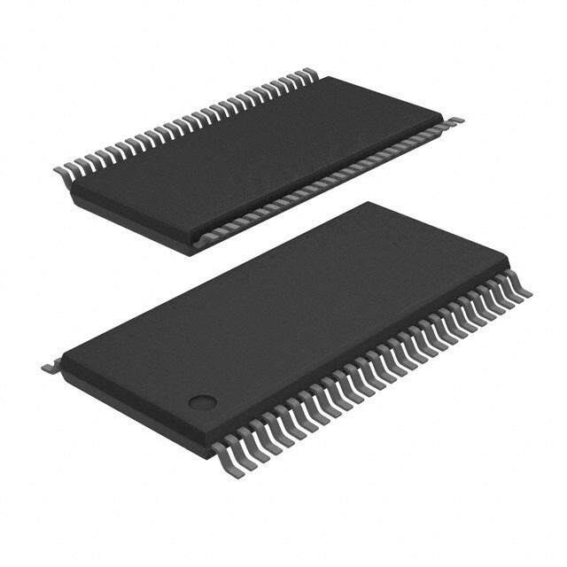
| 产品图片 |
|
| rohs | 符合RoHS无铅 / 符合限制有害物质指令(RoHS)规范要求 |
| 产品系列 | 接口 IC,LVDS 接口集成电路,Fairchild Semiconductor FIN212ACMLXµSerDes™ |
| 数据手册 | |
| 产品型号 | FIN212ACMLX |
| 产品目录页面 | |
| 产品种类 | LVDS 接口集成电路 |
| 供应商器件封装 | 32-MLP(5x5) |
| 其它名称 | FIN212ACMLXDKR |
| 功能 | 串行器/解串器 |
| 包装 | Digi-Reel® |
| 单位重量 | 300 mg |
| 商标 | Fairchild Semiconductor |
| 安装类型 | 表面贴装 |
| 安装风格 | SMD/SMT |
| 封装 | Reel |
| 封装/外壳 | 32-MLP |
| 封装/箱体 | MLP-32 |
| 工作温度 | -30°C ~ 70°C |
| 工作电源电压 | 3.3 V |
| 工厂包装数量 | 3000 |
| 数据速率 | 560Mbps |
| 最大工作温度 | + 70 C |
| 最小工作温度 | - 30 C |
| 标准包装 | 1 |
| 电压-电源 | 1.65 V ~ 3.6 V |
| 类型 | Serializer Deserializer with Multiple Frequency Range |
| 系列 | FIN212A |
| 输入数 | 12 |
| 输入类型 | LVCMOS |
| 输出数 | 12 |
| 输出类型 | LVCMOS |


- 商务部:美国ITC正式对集成电路等产品启动337调查
- 曝三星4nm工艺存在良率问题 高通将骁龙8 Gen1或转产台积电
- 太阳诱电将投资9.5亿元在常州建新厂生产MLCC 预计2023年完工
- 英特尔发布欧洲新工厂建设计划 深化IDM 2.0 战略
- 台积电先进制程称霸业界 有大客户加持明年业绩稳了
- 达到5530亿美元!SIA预计今年全球半导体销售额将创下新高
- 英特尔拟将自动驾驶子公司Mobileye上市 估值或超500亿美元
- 三星加码芯片和SET,合并消费电子和移动部门,撤换高东真等 CEO
- 三星电子宣布重大人事变动 还合并消费电子和移动部门
- 海关总署:前11个月进口集成电路产品价值2.52万亿元 增长14.8%


PDF Datasheet 数据手册内容提取
Sµ uS pe pr D March 2013 o re ts in™ g F C I FIN212AC aN m2 1 12-Bit Serializer / Deserializer Supporting Cameras and era2A C a Small Displays n — d s 1 m2 Features Description - aB Data & Control Bits 12-Bit ll Dit S Frequency 40MHz The FIN212AC µSerDes™ is a low-power serializer / ise Capability Camera or LCD deserializer optimized for use in cell phone displays and pri la Interface Microcontroller, RGB, YUV camera paths. The device reduces a 12-bit data path to four al µController Usage m68 & i86 wires. For camera applications, an additional master clock ysize Selectable Edge Rates Yes can be passed in the opposite direction of data flow. The r Standby Current <10 µA device utilizes Fairchild’s proprietary ultra-low power, low- / D Core Voltage (VDDA/S) 2.5 to 3.6V EMI technology. e I/O Voltage (V ) 1.65 to 3.6V s DDP e ESD (I/O to GND) 14kV r Applications ia 32-Terminal MLP Package li 42-Ball USS-BGA Slider, Folder, & Clamshell Mobile Handsets ze FIN212ACMLX r Ordering Information FIN212ACGFX Printers S Security Cameras u p p o Related Resources r t i n For samples and questions, please contact: g Interface@fairchildsemi.com. C a m Typical Application e r a s Internal Built-in voltage a translation n Termination d Camera S FIN212AC FIN212AC m Module a l l DeDe +-+- 2 +-+-+- 12-B12-B Dis Baseband serializerserializer12-Bit 12-Bit +-+- 2 +-+-+- it Serializerit Serializer plays CTL™ Up to 40MHz Isolates interface for signal integrity Camera Module Figure 1. Mobile Phone Example © 2008 Fairchild Semiconductor Corporation www.fairchildsemi.com FIN212AC • Rev. 1.1.1
µ S FIN212AC (Serializer DIRI=1) Pin Descriptions e r D Pin Name Description e s 0 Deserializer ™ DIRI Control to determine serializer or deserializer configuration. 1 Serializer Adjusts CTL drive to compensate for environmental conditions 0 Low drive (low power) F CTL_ADJ and length. 1 High drive (high power) IN 2 S0 Configure frequency range for the PLL. See Table 1 Serializer (DIRI=1) Control Pin. 1 2 S1 Configure frequency range for the PLL. See Table 1 Serializer (DIRI=1) Control Pin. A C PLL0 Divide or adjust the serial frequency. See Table 1 Serializer (DIRI=1) Control Pin. — PLL1 Divide or adjust the serial frequency. See Table 1 Serializer (DIRI=1) Control Pin. CKREF LV-CMOS clock input and PLL reference. 1 2 STROBE LV-CMOS strobe input for latching data (DP [1:12]) into the serializer on the rising edge. - B DP[1:12] LV-CMOS parallel data input. (GND input if not used) i CKSO+ CTL Differential serializer output bit clock. t S CKSO- CKSO+: Positive signal; CKSO-: Negative signal. e DSO+ CTL Differential serial output data signals. r i DSO- DSO+: Positive signal; DSO-: Negative signal. a CKSI+ CTL Differential deserializer input bit clock. li No connect unless in “clock pass-through” mode. z CKSI- CKSI+: Positive signal; CKSI-: Negative signal. e CKP LV-CMOS word clock output or Pixel clock output. No connect unless in “clock pass-through” mode. r / /DIRO LV-CMOS output, Inversion of DIRI in normal operation. Can be used to drive the DIRI signal No connect if not used. D of the deserializer where the interface needs to be turned around. e VDDP Power supply for parallel I/O. (All VDDP pins must be connected to VDDP) s e VDDS Power supply for serial I/O. r VDDA Power supply for core. ia GND All GND pins must be connected to ground. BGA: all GND pads. MLP: Pin 29 & GND PAD must be grounded. li z N/C No connect. (Do not connect to GND or VDD) e r Note: S 1. 0=GND; 1=VDDP u p p FIN212AC (Serializer DIRI=1) Pin Configurations o r t i J E n 1 2 3 4 5 6 D g B F A O E O C A DP[4] DP[2] GND CTL_ADJ N/C CKREF DP[3] DP[2] DP[1] GND CTL_ STR CKR /DIR ame r 2 1 0 9 8 7 6 5 a 3 3 3 2 2 2 2 2 s B DP[6] DP[5] DP[1] N/C STROBE /DIRO DP[4] 1 24 CKSO+ a n d DP[5] 2 23 CKSO- S C CKP N/C DP[3] N/C CKSO+ CKSO- m DP[6] 3 22 DSO+ SERIALIZER a l VDDP 4 21 DSO- l D D N/C DP[7] VDDP GND DSO- DSO+ i CKP 5 20 CKSI- s p GND PAD l DP[7] 6 19 CKSI+ a y E DP[8] DP[9] GND VDDS CKSI+ CKSI- s DP[8] 7 18 DIRI DP[9] 8 17 VDDS F DP[10] DP[11] N/C VDDA N/C DIRI 9 10 11 12 13 14 15 16 G DP[12] N/C PLL1 PLL0 S1 S0 10] 11] 12] LL1 LL0 S1 S0 DA P[ P[ P[ P P D D D D V 42-Ball BGA, 3.5 x 4.5mm, .5mm pitch (Top View) 32-pin MLP, 5 x 5mm, .5mm pitch (Top View) Figure 2. FIN212AC (Serializer DIRI=1) Pin Assignments (Top View) © 2008 Fairchild Semiconductor Corporation www.fairchildsemi.com FIN212AC • Rev. 1.1.1 2
µ S FIN212AC (Deserializer DIRI=0) Pin Descriptions e r D Pin Name Description e s 0 Deserializer ™ DIRI Control to determine serializer or deserializer configuration. 1 Serializer 0 Internal termination used F XTERM Control to determine if using internal or external termination I 1 External termination required on CKSI & DSI N 2 S0 Signals used to define the edge rate of parallel I/O. See Table 2 Deserializer (DIRI=0) Control Pin. 1 2 S1 Signals used to define the edge rate of parallel I/O. See Table 2 Deserializer (DIRI=0) Control Pin. A PWS0 Configure CKP pulse width. See Table 2 Deserializer (DIRI=0) Control Pin. C — PWS1 Configure CKP pulse width. See Table 2 Deserializer (DIRI=0) Control Pin. DP[1:12] LV-CMOS parallel data output. (N/C if not used) 1 2 CKP LV-CMOS word clock output or Pixel clock output. - DSI+ CTL Differential serial input data signals. B i DSI- DSI+: Positive signal; DSI-: Negative signal. t CKSI+ CTL Differential deserializer input bit clock. S e CKSI- CKSI+: Positive signal; CKSI-: Negative signal. r CKSO+ CTL Differential serializer output bit clock. No connect unless in “clock pass-through” mode. ia CKSO- CKSO+: Positive signal; CKSO-: Negative signal. li z CKREF LV-CMOS clock input and PLL reference. No connect unless in “clock pass-through” mode. e STROBE LV-CMOS strobe input for latching data into the serializer. No connect unless in “clock pass-through” mode. r /DIRO LV-CMOS Output. Inversion of DIRI in normal operation. No connect if not used. / D VDDP Power supply for parallel I/O. (All VDDP pins must be connected to VDDP) e VDDS Power supply for serial I/O. s VDDA Power supply for core. e r GND All GND pins must be connected to ground. BGA: all GND pads. MLP: Pin 28, 29, GND PAD must be grounded. ia N/C No connect. BGA: G1, F2; MLP: 10, 11; (Do not connect to GND or VDD) li z Note: e r 2. 0=GND; 1=VDDP S u p FIN212AC (Deserializer DIRI=0) Pin Configurations p o r t 1 2 3 4 5 6 i n E B F g A DP[4] DP[2] XTRM GND N/C CKREF DP[3] DP[2] DP[1] XTRM GND STRO CKRE DIRO Cam / e B DP[6] DP[5] DP[1] N/C STROBE /DIRO 32 31 30 29 28 27 26 25 ras DP[4] 1 24 CKSO+ a n DP[5] 2 23 CKSO- d C CKP N/C DP[3] N/C CKSO+ CKSO- S DP[6] 3 22 DSI- m DESERIALIZER a VDDP 4 21 DSI+ l l D N/C DP[7] VDDP GND DSI+ DSI- D CKP 5 20 CKSI- i s GND PAD p DP[7] 6 19 CKSI+ l a E DP[8] DP[9] GND VDDS CKSI+ CKSI- DP[8] 7 18 DIRI y s DP[9] 8 17 VDDS F DP[10] DP[11] N/C VDDA N/C DIRI 9 10 11 12 13 14 15 16 10] 11] 12] S1 S0 S1 S0 DA G DP[12] N/C PWS1 PWS0 S1 S0 DP[ DP[ DP[ PW PW VD 42-Ball BGA, 3.5 x 4.5mm, .5mm pitch (Top View) 32-pin MLP, 5mm x 5mm, .5mm pitch (Top View) Figure 3. FIN212AC (Deserializer DIRI=0) Pin Assignments (Top View) © 2008 Fairchild Semiconductor Corporation www.fairchildsemi.com FIN212AC • Rev. 1.1.1 3
µ S System Control Pin e r D e Function Control Pin s Conditions PLL ™ CKREF STROBE Multiplier PLL0 PLL1 S0 S1 F I Slow Frequencies N 2 Normal operation 5MHz to 14MHz ≤ CKREF (Up to 14MHz) 1 1 0 0 1 1 2 Supports spread spectrum on CKREF 4.7MHz to 13.3MHz ≤ CKREF (Up to 13.3MHz) 0.954 0 0 0 1 A C With a fixed CKREF input; STROBE can be 1/2 the speed 5MHz to 14MHz ≤ CKREF / 2 (Up to 7MHz) 2 0 1 0 1 — With a fixed CKREF input; STROBE 1 5MHz to 14MHz ≤ CKREF / 3 (Up to 4.67MHz) 3 1 1 0 1 2 can be 1/3 the speed - B Medium Frequencies i t Normal operation 8MHz to 28MHz ≤ CKREF (Up to 28MHz) 1 1 0 1 1 S e Supports spread spectrum on CKREF 9.5MHz to 26.7MHz ≤ CKREF (Up to 26.7MHz) 0.954 0 0 1 1 r i a With a fixed CKREF input; STROBE l 8MHz to 28MHz ≤ CKREF / 2 (Up to 14MHz) 2 0 1 1 1 i can be 1/2 the speed z e With a fixed CKREF input; STROBE 8MHz to 28MHz ≤ CKREF / 3 (Up to 9.3MHz) 3 1 1 1 1 r / can be 1/3 the speed D Fast Frequencies e s Normal operation 20MHz to 40MHz ≤ CKREF (Up to 40MHz) 1 1 0 1 0 e r i Supports spread spectrum on CKREF 19MHz to 38.2MHz ≤ CKREF (Up to 38.2MHz) 0.954 0 0 1 0 a l i With a fixed CKREF input; STROBE z 20MHz to 40MHz ≤ CKREF / 2 (Up to 20MHz) 2 0 1 1 0 e can be 1/2 the speed r S With a fixed CKREF input; STROBE 20MHz to 40MHz ≤ CKREF / 3 (Up to 13.3MHz) 3 1 1 1 0 u can be 1/3 the speed p p Power-Down X X 0 0 o r Table 1: Serializer (DIRI=1) Control Pin ti n g CKP Pulse Width Low Time Reference Control Pin C LVCMOS Output CKP to PLL CKREF=19.2 CKREF=26 Pwidth a Edge Rates STROBE MHz MHz Multiplier Multiplier PWS0 PWS1 S0 S1 m (Serializer) e Slow Frequencies ra s ~7 – 8ns (CL=8pF) Non-Inverted 52.1ns 38.5ns 2 7 0 0 0 1 a Inverted 52.1ns 38.5ns 2 7 1 0 0 1 nd [Typically for 5MHz to Non-Inverted 96.7ns 71.4ns 2 13 0 1 0 1 S 14MHz signals] m Non-Inverted 126.5ns 93.4ns 2 17 1 1 0 1 a l Medium Frequencies l D Non-Inverted 78.1ns 57.7ns 3 7 0 0 1 1 i ~4 – 5ns (C=8pF) s L p Inverted 78.1ns 57.7ns 3 7 1 0 1 1 l a [Typically for 8MHz to Non-Inverted 145.1ns 107.1ns 3 13 0 1 1 1 y s 28MHz signals] Non-Inverted 189.7ns 140.1ns 3 17 1 1 1 1 Fast Frequencies Non-Inverted 26ns 19.2ns 1 7 0 0 1 0 ~2 – 3ns (C=8pF) L Inverted 26ns 19.2ns 1 7 1 0 1 0 [Typically for 20MHz Non-Inverted 48.4ns 35.7ns 1 13 0 1 1 0 to 40MHz signals] Non-Inverted 63.2ns 46.7ns 1 17 1 1 1 0 Power-Down X X 0 0 Table 2: Deserializer (DIRI=0) Control Pin © 2008 Fairchild Semiconductor Corporation www.fairchildsemi.com FIN212AC • Rev. 1.1.1 4
µ S Pulse Width Calculations e r D CKP Pulse Width Low Time=(PLL Multiplier * Pwidth Multiplier) / (CKREF*14) (1) e s ™ Example: CKREF=26MHz; PLL Multiplier=2; Pwidth Multiplier=13 F CKP Pulse width=(2 * 13) / (26MHz * 14)=71.4ns (2) I N 2 1 2 Power-Down States A C When both S1 and S0 signals are 0, regardless of the state of the DIRI signal, the FIN212AC resets and powers down. The — power-down mode shuts down all internal analog circuitry, disables the serial input and output of the device, and resets all internal digital logic. Table 3: Power-Down indicates the state of the input states and output buffers in Power-Down mode. 1 2 - B Signal Pins DIRI=1 (Serializer) DIRI=0 (Deserializer) i t DP[12:1] Inputs Disabled High-Z S e CKP HIGH High-Z r i a STROBE Input Disabled Input Disabled l i z CKREF Input Disabled Input Disabled e r /DIRO 0 1 / D Table 3: Power-Down e s e r i a Clock Pass-Through Mode l i z e Clock pass-through mode allows a harmonic rich clock source to be sent to the serializer in a CTL format to reduce the overall r harmonic content of the phone, and can reduce the need for EMI filters. The Master Clock Pass through mode performs a S translation to the clock in the CTL link, and does not serialize this signal. The following describes how to enable this u p functionality for an image sensor (See Figure 6). p o Deserializer Configuration (DIRI=0) r t i n 1. Connect CKREF(BGA pin A6) to GROUND g 2. Connect master clock to STROBE (BGA pin B5) C a m Serializer Configuration (DIRI=1) e 1. CKSI passes master clock to CKP output (BGA pin C1) ra s a n d CKREF and STROBE Signals S Please note that there is a setup and hold time between STROBE and data that must be met as seen on the electrical m characteristics section. The relationship between CKREF and STROBE can be synchronous or asynchronous depending on a l what is available in the system. It is suggested that if the signals are synchronous and in normal operation that CKREF is tied l D to STROBE as close to the chip as possible. If you are running an asynchronous or spread spectrum setup, please be aware i s this may result on cycle jitter on the CKP signal. They cycle jitter does not effect the output data and clock relationship, the p display or end application should continue to work as normal. la y s PLL Note Please note that the PLL ranges can overlap, power consumption can be reduced by selecting the operation in the lower end of the higher speed PLL range. © 2008 Fairchild Semiconductor Corporation www.fairchildsemi.com FIN212AC • Rev. 1.1.1 5
µ S e r Application Diagrams D e s The following application diagrams illustrate the most typical applications for the FIN212 device. Specific configurations of the ™ control pins may vary based on the needs of a given system. The following recommendations are valid for all of the F applications shown. I N 2 FIN212AC FIN212AC 12 Serializer Deserializer A VDDP1 VDD VDDP2 C Baseband D3 E4 F4 E4 F4 D3 Processor LCD MODULE — VDDP VDDS/A VDDS/A VDDP PIXEL CLK A6 CKREF CKP C1 PIXEL CLK 12 B5 STROBE CKSO+ C5 E5 CKSI+ CKREF A6 -B NCC1 CKP CKSO- C6 E6 CKSI- STROBE B5 i t Data[7:0] B3:E1 DP[8:1] DSO+ D6 D5 DSI+ DP[8:1] B3:E1 Data[7:0] Se HSYNC E2 DP[9] DSO- D5 D6 DSI- DP[9] E2 HSYNC ri F1 F1 a VSYNC DP[10] DP[10] VSYNC l G1:F2 DP[12:11] DP[12:11] G1:F2 NC iz e VDDP1F6 DIRI CCKKSSII+- EE65NNCC NNCCCC65 CCKKSSOO+- XTDRIRMI AF63 /RES r / D G3 G3 PLL1 PWS1 e G4 B6 B6 G4 s A4 PLL0 /DIRO NC NC /DIRO PWS0 e CTL_ADJ r GG56 S1 S1 GG56 ial S0 S0 iz GND GND e r S /RES u p Figure 4. 8-Bit RGB Application (Example Shows BGA 42-Pin Package) p o r Serializer Configuration: Deserializer Configuration: ti n 8MHz to 28MHz Frequency Range (S1=S0=1) ~4 – 5ns output edge rates (S1=S0=1) g Normal Mode (PLL1=0; PLL0=1) ~50% CKP PW,(PWS1=PWS0=0) C a m FIN212AC FIN212AC Deserializer Serializer e VDDP1 VDD VDDP2 ra Baseband D3 E4 F4 E4 F4 D3 s Processor VDDP VDDS/A VDDS/A VDDP a n A6 CKP CKP C1 NC Camera Module d PIXEL CLK BC51 CSTKRROEFBE CCKKSSOO+- CC56NNCCNNCCEE56 CCKKSSII+- STCRKORBEEF AB65 MPIAXSETLE CRL KCLK Sm YUV[7:0] B3:E1 DP[8:1] DSI+ D5 D6 DSO+ DP[8:1] B3:E1 YUV[7:0] al HSYNC E2 DP[9] DSI- D6 D5 DSO- DP[9] E2 HSYNC l D VSYNC F1 DP[10] DP[10] F1 VSYNC i NC G1:F2 DP[12:11] CKSI- EE65 CC65 CKSO- DP[12:11] G1:F2 /RES sp CKSI+ CKSO+ VDDP2 l FG63 DPWIRSI1 /DIRO BN6C NCB6 /DIRO PDLILR1I FG63 ays G4 PWS0 PLL0 G4 A3 XTRM CTL_ADJ A4 G5 S1 S1 G5 G6 G6 S0 S0 GND GND /RES Figure 5. 8-Bit YUV 1.3MPixel CMOS Imager (Example Shows BGA 42-Pin Package) Deserializer Configuration: Serializer Configuration: ~2 – 3ns output edge rates (S1=0, S0=1) 20MHz to 40MHz Frequency Range (S1=0, S0=1) ~50% CKP PW,(PWS1=PWS0=0) Normal Mode (PLL1=0, PLL0=1) © 2008 Fairchild Semiconductor Corporation www.fairchildsemi.com FIN212AC • Rev. 1.1.1 6
µ S e r Application Diagrams (Continued) D e s ™ FIN212AC FIN212AC Deserializer Serializer F VDDP1 VDD VDDP2 IN Baseband D3 E4 F4 E4 F4 D3 2 Processor VDDP VDDS/A VDDS/A VDDP Camera Module 12 A6 CKREF CKP C1 MASTER CLK A MASTER CLK B5 STROBE CKSO+ C5 E5 CKSI+ CKREF A6 C PIXEL CLK C1 CKP CKSO- C6 E6 CKSI- STROBE B5 PIXEL CLK — YUV[7:0] B3:E1 DP[8:1] DSI+ D5 D6 DSO+ DP[8:1] B3:E1 YUV[7:0] 12 HVSSYYNNCC NC EFG121:F2 DDDPPP[[[911]02]:11] CDKSSII-- DE66 D5C6 DCSKOSO-- DP[D1DP2P:[11[109]]] EFG121:F2 HV/RSSEYYSNNCC -Bit E5 C5 S CKSI+ CKSO+ VDDP2 e F6 DIRI DIRI F6 r G3 PWS1 /DIRO BN6C NCB6 /DIRO PLL1 G3 ia G4 PWS0 PLL0 G4 liz A3 XTRM CTL_ADJ A4 e G5 G5 r G6 SS10 SS10 G6 / D GND GND e s /RES e r i a Figure 6. 8-Bit YUV 1.3MPixel CMOS Imager In Clock Pass-Through Mode l i z e Serializer Configuration: Deserializer Configuration: r 20MHz to 40MHz Frequency Range (S1=0, S0=1) ~2 – 3ns output edge rates (S1=0, S0=1) S u Normal Mode (PLL1=0; PLL0=1) ~50% CKP PW,(PWS1=PWS0=0) p p Master clock bypass mode. o r t FIN212AC FIN212AC in Serializer Deserializer g VDDP1 VDD VDDP2 Baseband C D3 E4 F4 E4 F4 D3 a Processor VDDP VDDS/A VDDS/A VDDP MAIN LCD m SYS CLK A6 CKREF CKP C1 /WE er /WE B5 STROBE CKSO+ C5 E5 CKSI+ CKREF A6 DATA[7:0] a NCC1 CKP CKSO- C6 E6 CKSI- STROBE B5 A0 s a /CS n Data[7:0] B3:E1 DP[8:1] DSO+ D6 D5 DSI+ DP[8:1] B3:E1 /RES d A0 E2 DP[9] DSO- D5 D6 DSI- DP[9] E2 S F1 DP[10] DP[10] F1NC m /CS0 F2 DP[11] DP[11] F2 a /CS1 VDDGP11 DP[12] CKSI- E6NC NCC6 CKSO- DP[12] G1 ll D FG63 DIRI CKSI+ E5NC NCC5 CKSO+ XTRM AF63 SUB LCD is PLL1 DIRI p G4 PLL0 /DIRO B6NC NCB6 /DIRO PWS1 G3 /WE la AG45 CTL_ADJ PWS0 G4 DATA[7:0] ys G6 S1 G5 A0 S0 GND S1 G6 /CS GND S0 /RES /RES Figure 7. 8-Bit WRITE-Only Microcontroller Interface (Example Shows BGA 42-Pin Package) Serializer Configuration: Deserializer Configuration: 20MHz to 40MHz Frequency Range (S1=0, S0=1) ~7 – 8ns output edge rates (S1=1, S0=0) CKREF is twice as fast STROBE (PLL1=1; PLL0=0) ~50% CKP PW,(PWS1=PWS0=0) CKREF=26MHz & STROBE Frequency=10 MHz © 2008 Fairchild Semiconductor Corporation www.fairchildsemi.com FIN212AC • Rev. 1.1.1 7
µ S Additional Application Information e r D e Flex Cabling: The serial I/O information is transmitted at a high serial rate. Care must be taken implementing this serial I/O s ™ flex cable. The following best practices should be used when developing the flex cabling or Flex PCB. F Keep all four differential Serial Wires the same length. IN 2 Do not allow noisy signals over or near differential serial wires. 1 2 Example: No LVCMOS traces over differential serial wires. A Use only one ground plane or wire over the differential serial wires. Do not run ground over top and bottom. C — Design goal of 100 differential characteristic impedance. 1 Do not place test points on differential serial wires. 2 - B Use differential serial wires a minimum of 2cm away from the antenna. i t For additional applications notes or flex guidelines see your sales representative or contact Fairchild directly. S e For samples and questions, please contact: Interface@fairchildsemi.com. ri a l i z Absolute Maximum Ratings e r / Stresses exceeding the absolute maximum ratings may damage the device. The device may not function or be operable above D the recommended operating conditions and stressing the parts to these levels is not recommended. In addition, extended e s exposure to stresses above the recommended operating conditions may affect device reliability. The absolute maximum e r ratings are stress ratings only. i a l i Symbol Parameter Min. Max. Unit z e VDD Supply Voltage -0.5V +4.6 V r S All Input/Output Voltage -0.5 VDD+0.5 V u p CTL Output Short-Circuit Duration Continuous p o TSTG Storage Temperature Range -65 +150 °C r t TJ Maximum Junction Temperature +150 °C in g TL Lead Temperature (Soldering, four seconds) +260 °C C Serial I/O Pins to GND 14 kV a Human Body Model JESD22-A114 m ESD All Pins 8 kV e Charged Device Model, JESD22-C101 2 kV ra s Recommended Operating Conditions a n d The Recommended Operating Conditions table defines the conditions for actual device operation. Recommended operating S conditions are specified to ensure optimal performance to the datasheet specifications. Fairchild does not recommend m exceeding them or designing to Absolute Maximum Ratings. a l l Symbol Parameter Min. Max. Unit D i V , V Supply Voltage 2.5 3.6 V s DDA DDS p VDDP Supply Voltage 1.65 3.60 V la y TA Operating Temperature -30 +70 ºC s V Supply Noise Voltage 100 mV DDA-PP PP DC Electrical Characteristics Values are provided for over-supply voltage and operating temperature ranges, unless otherwise specified. Symbol Parameter Test Conditions Min. Typ.(3) Max. Unit LVCMOS I/O VIH Input High Voltage 0.65xVDDP VDDP VIL Input Low Voltage GND 0.35xVDDP V © 2008 Fairchild Semiconductor Corporation www.fairchildsemi.com FIN212AC • Rev. 1.1.1 8
µ S DC Electrical Characteristics (Continued) er D I =-2.0mA, S1=0,S0=1 e OH s V Output High Voltage I =-0.4mA, S1=1,S0=0 0.75xV V V ™ OH OH DDP DDP I =-1.0mA, S1=1,S0=1 F OH I N I =2.0mA, S1=0,S0=1 OL 2 V Output Low Voltage I =0.4mA, S1=1,S0=0 0 0.25xV V 1 OL OL DDP 2 I =1.0mA, S1=1,S0=1 A OL C IIN Input Current VIN= 0V to 3.6V -5.0 5.0 µA — DIFFERENTIAL I/O 1 IODH OSouutprcuet HCIuGrHre nt VOS=1.0V CCTTLL__AADDJJ==01 -3-2.4 mA 2-B i t Output LOW CTL_ADJ=0 1.2 S IODL Sink Current VOS=1.0V CTL_ADJ=1 2 mA er i VGO Input Voltage Ground Offset(4) 0 V ali z CKS Internal Receiver VID=50mV, VIC=925mV, e RTRM Termination Resistor DIRI=0 80 100 120 Ω r / D DS Internal Receiver VID=50mV, VIC=925mV, 80 100 120 Ω e Termination Resistor DIRI=0 s e Notes: r i a 3. Typical values are given for V =2.775V and T =25°C. Positive current values refer to the current flowing into the device DD A li and negative values refer to the current flowing out of pins. Voltages are referenced to GROUND unless otherwise z e specified (except ΔVOD and VOD). r 4. V is the difference in device ground levels between the CTL driver and the CTL receiver. S GO u p Power Supply Currents p o r Symbol Parameter Test Conditions Min. Typ. Max. Unit t i n IDD_PD VDD Power-Down Supply Current S1=S0=0, All Inputs at GND or VDD 0.1 µA g S1=L 20MHz 13 mA C a S0=H 40MHz 19 mA m IDD_SER1 DCyunrraemnti c Serializer Power Supply fCCTKRLE_F=AfDSTJR=B0, ;P CLLL=10=p0F,P LL0=1; SS10==HL 51M4MHHz z 91.75 mmAA eras S1=H 8MHz 11 mA a n S0=H 28MHz 20 mA d S S1=L 20MHz 10 mA m S0=H 40MHz 14 mA a l I Dynamic Deserializer Power fCKREF=fSTRB, PLL1=0,PLL0=1; S1=H 5MHz 8 mA l D DD_DES1 Supply Current CTL_ADJ=0; CL=0pF S0=L 14MHz 9 mA is p S1=H 8MHz 9 mA l a S0=H 28MHz 12 mA y s Pin Capacitance Tables Symbol Parameter Test Conditions Min. Typ. Max. Unit Capacitance of Input Only Signals; Parallel DIRI=1, S1=0, S0=0, C , C , C 2 pF IN IO IO-DIFF Port Pins DP[1:10]; Differential I/O V =2.5V DD © 2008 Fairchild Semiconductor Corporation www.fairchildsemi.com FIN212AC • Rev. 1.1.1 9
µ S e r AC Electrical Characteristics D e Values are provided for over-supply voltage and operating temperature ranges, unless otherwise specified. s ™ Symbol Parameter Test Conditions Min. Typ. Max. Unit F I Serializer Input Operating Conditions N 2 S1=0, S0=1 18 40 1 CKREF Clock Frequency 2 f f =f S1=1, S0=0 5 14 MHz A CKREF (5MHz - >40MHz); CKREF STRB C S1=1, S0=1 10 28 — PLL1=0, PLL0=0 100 1 Strobe Frequency Relative to PLL1=0, PLL0=1 100 % of 2 fSTRB CKREF Frequency fCKREF ≠ fSTRB PLL1=1, PLL0=0 50 fCKREF -B i PLL1=1, PLL0=1 331/3 t S t CKREF DC T=1/f 0.2 0.5 0.8 T e CPWH CKREF r i t CKREF DC T=1/f 0.2 0.5 0.8 T a CPWL CKREF l t LVCMOS Input Transition Time(5) 10-90% 20 ns iz CLKT e tSPWH/L STROBE Pulse Width HIGH/LOW T=1/fCKREF T x 4/14 T x 10/14 ns r / SetupTime t D STC e DP Setup to STROBE (n) s tSTC STROBE 2.5 ns e (DIRI=1, f=5MHz) DP[1:12] Data ri a l i HoldTime t z HTC e DP(n) Hold to STROBE r tHTC (DIRI=1, f=5MHz) STROBE 2.0 ns S u DP[1:12] Data p p Serializer AC Electrical Characteristics o tTCCD rti n STROBE t g VDD/2 RCCD C CKS- Transmitter Clock Input to Clock a tTCCD Output Delay(6) CKS+ VDIFF=0 21a+1.5 23a+6.5 ns m CKP e VDD/2 r a Note:STROBE=CKREF s DIRI=1, fCKREF=fSTRB a n Phase Lock Loop (PLL) AC Electrical Characteristics d t Serializer PLL Stabilization Time CKREF toggling and stable 200 600 μs S TPLLS0 m t PLL Disable Time Loss of Clock 30.0 μs TPLLD0 a l t PLL Power-Down Time 20.0 ns l TPLLD1 D Deserializer AC Electrical Characteristics i s Symbol Parameter Test Conditions Min. Typ. Max. Unit p l a DataValid t PWS1 PWS0 y PDV s CKP fSTRB=fCKREF 0 0 7a-3 7a+3 t f =f 0 1 7a-3 7a+3 ns RCOL STRB CKREF DP[1:12] Data f =.5x f 1 0 13a-3 13a+3 STRB CKREF f =.5x f 1 1 17a-3 17a+3 t STRB CKREF RCOP 75% CKP 50% 50% 25% Data Valid to CKP HIGH (Rising Edge t 8a-3 8a+3 ns PDV STROBE), C=5pF tRCOH tRCOL L Setup:DIRI=0, CKSIandDSarevalidsignals. © 2008 Fairchild Semiconductor Corporation www.fairchildsemi.com FIN212AC • Rev. 1.1.1 10
µ S AC Electrical Characteristics (Continued) er D e S1=0,S0=1 3 s Output Rise/Fall Time Data ™ t C=8pF S1=1,S0=0 8 ns RFD (20% to 80%) L S1=1,S0=1 5 F I N S1=0,S0=1 2 2 Output Rise/Fall Time CKP 1 tRFC (20% to 80%) CL=8pF S1=1,S0=0 7 ns 2 A S1=1,S0=1 4 C Notes: — 5. Parameter is characterized, but not production tested. 6. The average bit time “a” is a function of the serializer CKREF frequency; a=(1/f)/14. 1 2 - B Logic Timing Controls i t S Symbol Parameter Test Conditions Min. Typ. Max. Unit e r t , i PHL_DIR Propagation Delay DIRI to /DIRO DIRI L->H or H->L 17 ns a tPLH_DIR li z t , t Propagation Delay DIRI to DP DIRI L->H or H->L 25 ns e PLZ PHZ r Deserializer Disable Time: S0 or S1 LOW to DPTri-State; DIRI=0, / D tDISDES e s e r tDISDES S1orS0 25 ns ia l i z e DP r S Note:IfS0(2)istransitioning,S1(1)must=0fortesttobevalid. u p tDISSER Serializer Disable Time: S0 or S1 LOW to CKP HIGH DIRI=1; S1(0) and S0(1)=H->L 25 ns p o r t i n g C a m e r a s a n d S m a l l D i s p l a y s © 2008 Fairchild Semiconductor Corporation www.fairchildsemi.com FIN212AC • Rev. 1.1.1 11
µ S Tape and Reel Specifications e r D MLP Embossed Tape Dimensions e s ™ F I N 2 1 2 A C — 1 2 - B i t Package A0 B0 D D1 E F K0 P1 P0 P2 T TC W WC S ±0.1 ±0.1 ±0.5 Min. ±0.1 ±0.1 ±0.1 Typ. Typ. ±0.5 Typ. ±0/05 ±0.3 Typ. e r 5 x 5 5.35 5.35 1.55 1.50 1.75 5.50 1.40 8.00 4.00 2.00 0.30 0.07 12.00 9.30 ia l 6 x 6 5.35 5.35 1.55 1.50 1.75 5.50 1.40 8.00 4.00 2.00 0.30 0.07 12.00 9.30 i z e Notes: r A , B , and K dimensions are determined with respect to the EIA/JEDEC RS-481 rotational and lateral movement / 0 0 0 D requirements (see sketches A, B, and C). e s MLP Shipping Reel Dimensions e r i a l i z e r S u p p o r t i n g C a m e r a s a n d S m a l l D i s p l a y s Dia A Dim B Dia C Dia D Dim N Dim W1 Dim W3 Tape Width Dim W2 Max. Min. +0.5/-0.2 Min. Min. +2.0/-0 (LSL-USL) 8 330.0 1.5 13.0 20.2 178.0. 8.4 14.4 7.9 ~ 10.4 12 330.0 1.5 13.0 20.2 178.0. 12.4 18.4 11.9 ~ 15.4 16 330.0 1.5 13.0 20.2 178.0. 16.4 22.4 15.9 ~ 19.4 Figure 8. MLP Tape and Reel © 2008 Fairchild Semiconductor Corporation www.fairchildsemi.com FIN212AC • Rev. 1.1.1 12
µ S e r Tape and Reel Specifications (Continued) D e s ™ BGA Embossed Tape Dimensions F I N 2 1 2 A C — 1 2 - B i t S e r ia l i Package A B D D E F K P P P T T W W z 0 0 1 0 1 0 2 C C e ±0.1 ±0.1 ±0.5 Min. ±0.1 ±0.1 ±0.1 Typ. Typ. ±0.5 Typ. ±0/05 ±0.3 Typ. r / 3.5 x 4.5 3.85 4.80 1.55 1.50 1.75 5.50 1.10 8.00 4.00 2.00 0.30 0.07 12.00 9.3 D Notes: e s A0, B0, and K0 dimensions are determined with respect to the EIA/JEDEC RS-481 rotational and lateral movement e requirements (see sketches A, B, and C). ri a l i z e BGA Shipping Reel Dimensions r S u p p o r t i n g C a m e r a s a n d S m a l l D i s p l a y s Dia A Dim B Dia C Dia D Dim N Dim W1 Dim W3 Tape Width Dim W2 Max. Min. +0.5/-0.2 Min. Min. +2.0/-0 (LSL-USL) 8 330.0 1.5 13.0 20.2 178.0. 8.4 14.4 7.9 ~ 10.4 12 330.0 1.5 13.0 20.2 178.0. 12.4 18.4 11.9 ~ 15.4 16 330.0 1.5 13.0 20.2 178.0. 16.4 22.4 15.9 ~ 19.4 Figure 9. BGA Tape and Reel © 2008 Fairchild Semiconductor Corporation www.fairchildsemi.com FIN212AC • Rev. 1.1.1 13
µ S Physical Dimensions e r D e 0.15 C s 5.00 B ™ A F I N 2 1 5.00 2 (0.76) A (0.25 ) C PIN #1 IDENT — 1 5.38 MIN 2 0.15 C - 3.37 MAX B i 3.86 MIN t S e 0.10C 0.80 MAX (0.20) 0X.240MIN ria l i z 0.08C00..0050 C 0.28 MAX 0.50TYP er SEATING X40 E / PLANE D 3.70 3.50 e s 0.45 e PIN #1 IDENT 0.35 PIN #1 ID ri a l i z e 0.50 r S 33..7500 u (DATUM B) PIN #1 ID p p (DATUM A) o r t i n g 0.18-0.30 0.50 0.10 CAB C 0.05 C a m NOTES: e r a A. CONFORMS TO JEDEC REGISTRATION MO-220, VARIATION s WHHD-4. THIS PACKAGE IS ALSO FOOTPRINT COMPATIBLE WITH WHHD-5. a n B. DIMENSIONS ARE IN MILLIMETERS. d C. DIMENSIONS AND TOLERANCES PER ASME Y14.5M-1994. S D. LAND PATTERN PER IPC SM-782. m E. WIDTH REDUCED TO AVOID SOLDER BRIDGING. a l F. DIMENSIONS ARE NOT INCLUSIVE OF BURRS, MOLD FLASH, OR l D TIE BAR PROTRUSIONS. i G. DRAWING FILENAME: MKT-MLP32Arev3. s p l Figure 10. 32-Lead, Molded Leadless Package (MLP) a y s Order Number Operating Temperature Range Package Description Packing Method 32-Terminal Molded Leadless Package (MLP), FIN212ACMLX -30 to 70°C Tape & Reel Quad, JEDEC MO-220, 5mm Square Package drawings are provided as a service to customers considering Fairchild components. Drawings may change in any manner without notice. Please note the revision and/or date on the drawing and contact a Fairchild Semiconductor representative to verify or obtain the most recent revision. Package specifications do not expand the terms of Fairchild’s worldwide terms and conditions, specifically the warranty therein, which covers Fairchild products. Always visit Fairchild Semiconductor’s online packaging area for the most recent package drawings: http://www.fairchildsemi.com/packaging/. © 2008 Fairchild Semiconductor Corporation www.fairchildsemi.com FIN212AC • Rev. 1.1.1 14
µ S e r Physical Dimensions (Continued) D e s ™ F I N 2 1 2 A C — 1 2 - B i t S e r i a l i z e r / D e s e r i a l i z e r S u p p o r t i n g C a m e r a s a n d S m a l l D i s p l a y Figure 11. 42-Ball, Ball Grid Array (BGA) Package s Packing Order Number Operating Temperature Range Package Description Method 42-Ball Ultra Small-Scale Ball Grid Array (USS-BGA), FIN212ACGFX -30 to 70°C Tape & Reel JEDEC MO-195, 3.5 x 4.5mm Wide, 0.5mm Ball Pitch Package drawings are provided as a service to customers considering Fairchild components. Drawings may change in any manner without notice. Please note the revision and/or date on the drawing and contact a Fairchild Semiconductor representative to verify or obtain the most recent revision. Package specifications do not expand the terms of Fairchild’s worldwide terms and conditions, specifically the warranty therein, which covers Fairchild products. Always visit Fairchild Semiconductor’s online packaging area for the most recent package drawings: http://www.fairchildsemi.com/packaging/. © 2008 Fairchild Semiconductor Corporation www.fairchildsemi.com FIN212AC • Rev. 1.1.1 15
µ S e r D e s ™ F I N 2 1 2 A C — 1 2 - B i t S e r i a l i z e r / D e s e r i a l i z e r S u p p o r t i n g C a m e r a s a n d S m a l l D i s p l a y s © 2008 Fairchild Semiconductor Corporation www.fairchildsemi.com FIN212AC • Rev. 1.1.1 16