 Datasheet下载
- 型号: F921V224MAA
- 制造商: AVX
- 库位|库存: xxxx|xxxx
- 要求:
| 数量阶梯 | 香港交货 | 国内含税 |
| +xxxx | $xxxx | ¥xxxx |
查看当月历史价格
查看今年历史价格
F921V224MAA产品简介:
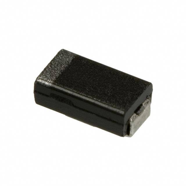
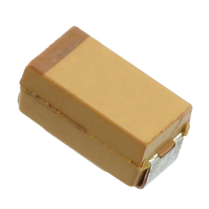
ICGOO电子元器件商城为您提供F921V224MAA由AVX设计生产,在icgoo商城现货销售,并且可以通过原厂、代理商等渠道进行代购。 F921V224MAA价格参考。AVXF921V224MAA封装/规格:钽电容器, 0.22µF 模制 钽电容器 35V 1206(3216 公制) 10 欧姆。您可以下载F921V224MAA参考资料、Datasheet数据手册功能说明书,资料中有F921V224MAA 详细功能的应用电路图电压和使用方法及教程。
AVX Corporation生产的钽电容器型号F921V224MAA是一种固态钽电容器,其主要应用场景包括以下领域:

 1. 电源滤波
   - 该型号的钽电容器具有低ESR(等效串联电阻)和高频率稳定性,非常适合用于电源电路中的滤波。例如,在开关电源、稳压器或DC-DC转换器中,它可以有效减少电压波动和噪声干扰。

 2. 信号耦合与解耦
   - 在高频信号处理电路中,F921V224MAA可用于信号耦合和解耦。它能够隔离直流成分,同时允许交流信号通过,确保信号传输的稳定性和纯净度。

 3. 消费电子设备
   - 此型号广泛应用于智能手机、平板电脑、笔记本电脑和其他便携式电子设备中。它的小型化设计和高可靠性使其成为这些设备的理想选择,特别是在需要紧凑空间和高效性能的场景下。

 4. 汽车电子系统
   - 在汽车电子领域,F921V224MAA可用于车载信息娱乐系统、导航设备、传感器模块以及发动机控制单元(ECU)。其耐高温和抗振动特性能够适应复杂的汽车环境。

 5. 工业自动化
   - 在工业控制设备中,如PLC(可编程逻辑控制器)、变频器和伺服驱动器,该钽电容器可用于平滑电源电压、滤除电磁干扰(EMI),从而提高系统的稳定性和可靠性。

 6. 医疗设备
   - 对于需要高精度和可靠性的医疗设备(如心率监测仪、超声波设备和植入式医疗器械),F921V224MAA的高稳定性和长寿命特性非常适用。

 7. 通信设备
   - 在通信基站、路由器和交换机等设备中,该型号可用于电源管理模块和信号处理电路,提供稳定的电容支持,确保通信质量。

总结来说,F921V224MAA凭借其高容量密度、低漏电流和优异的温度特性,适用于各种对性能和可靠性要求较高的电子设备和系统中。
| 参数 | 数值 |
| 产品目录 | |
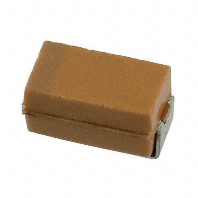
| 描述 | CAP TANT 0.22UF 35V 20% 1206钽质电容器-固体SMD 35volts 0.22uF 3.2x1.6 |
| ESR | 10 Ohms |
| ESR(等效串联电阻) | 10 欧姆 |
| 产品分类 | |
| 品牌 | AVX |
| 产品手册 | |
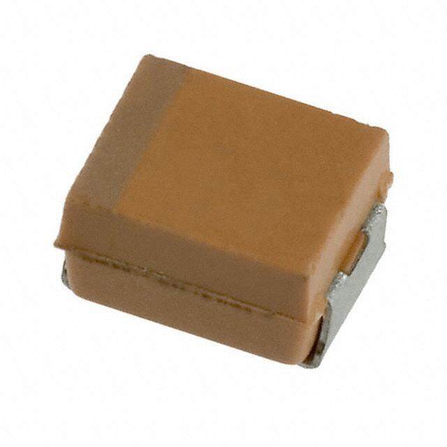
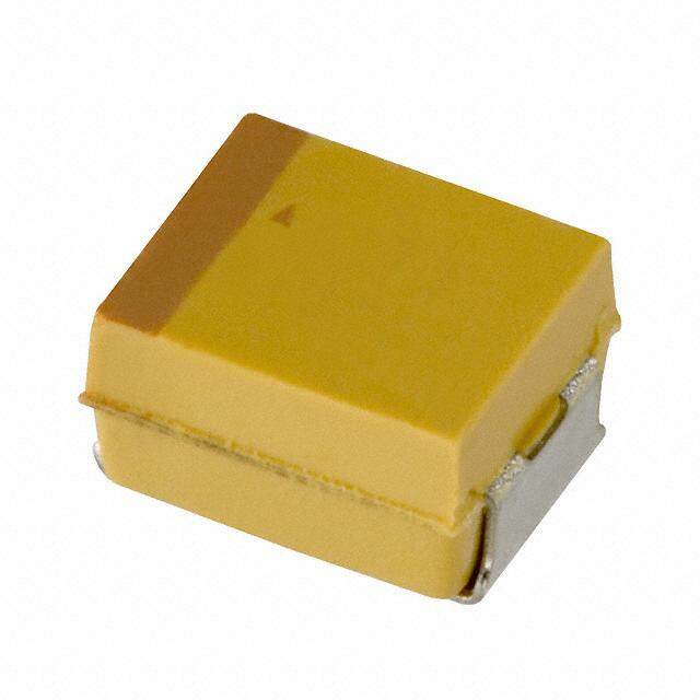
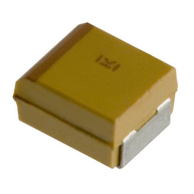
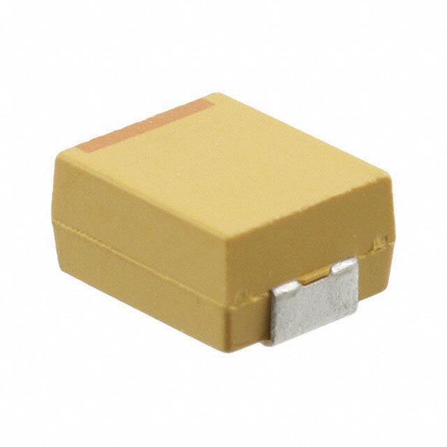
| 产品图片 |
|
| rohs | 符合RoHS无铅 / 符合限制有害物质指令(RoHS)规范要求 |
| 产品系列 | 钽电容器,钽质电容器-固体SMD,AVX F921V224MAAF92 |
| 数据手册 | |
| 产品型号 | F921V224MAA |
| PCN制造商信息 | |
| 不同温度时的使用寿命 | - |
| 产品 | Tantalum Solid Standard Grade - Other Various |
| 产品种类 | 钽质电容器-固体SMD |
| 其它名称 | 478-8130-1 |
| 制造商尺寸代码 | A |
| 制造商库存号 | A Case |
| 包装 | 剪切带 (CT) |
| 商标 | AVX |
| 外壳代码-in | 1206 |
| 外壳代码-mm | 3216 |
| 外壳宽度 | 1.6 mm |
| 外壳长度 | 3.2 mm |
| 大小/尺寸 | 0.126" 长 x 0.063" 宽(3.20mm x 1.60mm) |
| 安装类型 | 表面贴装 |
| 容差 | 20 % |
| 封装 | Reel |
| 封装/外壳 | 1206(3216 公制) |
| 封装/箱体 | 1206 (3216 metric) |
| 工作温度 | -55°C ~ 125°C |
| 工作温度范围 | - 55 C to + 125 C |
| 工厂包装数量 | 2500 |
| 引线间距 | - |
| 标准包装 | 1 |
| 特性 | 通用 |
| 电压-额定 | 35V |
| 电压额定值 | 35 V |
| 电容 | 0.22 uF |
| 端接类型 | SMD/SMT |
| 类型 | 模制 |
| 系列 | F92 |
| 高度 | 1.1 mm |
| 高度-安装(最大值) | 0.051"(1.30mm) |


- 商务部:美国ITC正式对集成电路等产品启动337调查
- 曝三星4nm工艺存在良率问题 高通将骁龙8 Gen1或转产台积电
- 太阳诱电将投资9.5亿元在常州建新厂生产MLCC 预计2023年完工
- 英特尔发布欧洲新工厂建设计划 深化IDM 2.0 战略
- 台积电先进制程称霸业界 有大客户加持明年业绩稳了
- 达到5530亿美元!SIA预计今年全球半导体销售额将创下新高
- 英特尔拟将自动驾驶子公司Mobileye上市 估值或超500亿美元
- 三星加码芯片和SET,合并消费电子和移动部门,撤换高东真等 CEO
- 三星电子宣布重大人事变动 还合并消费电子和移动部门
- 海关总署:前11个月进口集成电路产品价值2.52万亿元 增长14.8%


PDF Datasheet 数据手册内容提取
F92 Series Resin-Molded Chip, Low Profile J-Lead FEATURES • Compliant to the RoHS2 directive 2011/65/EU • SMD J-lead • Low profile case sizes LEAD-FREE COMPATI- APPLICATIONS COMBPLOENENT • Handheld electronics • USB accessories CASE DIMENSIONS:millimeters (inches) Code EIA Code EIA Metric L W1 W2 H S 3.20 ± 0.20 1.60 ± 0.20 1.20 ± 0.10 1.10 ± 0.10 0.80 ± 0.20 A 1206 3216-12 (0.126 ± 0.008) (0.063 ± 0.008) (0.047 ± 0.004) (0.043 ± 0.004) (0.031 ± 0.008) 3.40 ± 0.20 2.80 ± 0.20 2.30 ± 0.10 1.10 ± 0.10 0.80 ± 0.20 B 1311 3428-12 (0.134 ± 0.008) (0.110 ± 0.008) (0.091 ± 0.004) (0.043 ± 0.004) (0.031 ± 0.008) 2.00 ± 0.20 1.25 ± 0.10 0.90 ± 0.10 1.10 ± 0.10 0.50 ± 0.20 P 0805 2012-12 (0.079 ± 0.008) (0.049 ± 0.004) (0.035 ± 0.004) (0.043 ± 0.004) (0.020 ± 0.008) MARKING L W1 H P CASE A CASE B CASE *Rated Capacitance Rated Capacitance Rated Capacitance Code Code (µF) W2 S S A S G 226 22 10V Rated Voltage Rated Voltage Rated Voltage Code Code (V) 4V G 16V C 35V V 6.3V J 20V D 10V A 25V E *Capacitance code of “P” case products are as shown below. HOW TO ORDER F92 0J 106 M P (cid:2) LZT Type Rated Capacitance Tolerance Case Packaging Specification Voltage Code K = ±10% Size See Tape & Reel Suffix pF code: 1st two digits M = ±20% See Packaging Section Rated temperature represent significant figures, table 60ºC only 3rd digit represents multiplier above (number of zeros to follow) TECHNICAL SPECIFICATIONS Category Temperature Range: -55 to +125°C Rated Temperature: +85°C Capacitance Tolerance: ±20%, ±10% at 120Hz Dissipation Factor: Refer to next page ESR 100kHz: Refer to next page Leakage Current: After 1 minute’s application of rated voltage, leakage current at 20°C is not more than 0.01CV or 0.5μA, whichever is greater. After 1 minute’s application of rated voltage, leakage current at 85°C is not more than 0.1CV or 5μA, whichever is greater. After 1 minute’s application of derated voltage, leakage current at 125°C is not more than 0.125CV or 6.3μA, whichever is greater. Capacitance Change By Temperature P Case A, B Case +20% Max. at +125ºC +15% Max. at +125°C +15% Max. at +85ºC +10% Max. at +85°C -15% Max. at -55ºC -10% Max. at -55°C 010418 25
F92 Series Resin-Molded Chip, Low Profile J-Lead CAPACITANCE AND RATED VOLTAGE RANGE (LETTER DENOTES CASE SIZE) Capacitance Rated Voltage *Cap µF Code 4V (0G) 6.3V (0J) 10V (1A) 16V (1C) 20V (1D) 25V (1E) 35V (1V) Code 0.22 224 A J 0.33 334 A N 0.47 474 P A/P A S 0.68 684 P A W 1.0 105 P P A/P A/P A A 1.5 155 P P A E 2.2 225 P P A/P A A/B B J 3.3 335 P P A/P A B N 4.7 475 P P A/P A/B A(M)/B A/B S 6.8 685 P P A/P B w 10 106 A/P A/P A/P(M) A/B B a 15 156 P A/P(M) A e 22 226 A/P(M) A/P(M) A/B B J 33 336 A/P(M) A/B B n 47 476 A/B A/B B s 68 686 A(M)/B w 100 107 A(M)/B A(M)**/B A 150 157 B(M) E 220 227 J Released ratings (M tolerance only) **Rated temperature 60ºC only. Please contact AVX when you need detail spec. Please contact to your local AVX sales office when these series are being designed in your application. 26 051718
F92 Series Resin-Molded Chip, Low Profile J-Lead RATINGS & PART NUMBER REFERENCE Rated DF ESR *1 Rated DF ESR *1 AVX Case Capacita n c e Voltage DCL @ 120Hz @ 100kHz ΔC/C MSL AVX Case Capacita n c e Voltage DCL @ 120Hz @ 100kHz ΔC/C MSL P a r t N o . S i z e ( μ F ) (V) ( μ A ) (%) (Ω) (%) P a r t N o . S i z e ( μ F ) (V) ( μ A ) (%) (Ω) (%) 4 Volt F921A106MPA P 10 10 1.0 14 6.0 * 1 F920G335#PA P 3.3 4 0.5 8 12.0 * 1 F921A156#AA A 15 10 1.5 8 4.0 * 1 F920G475#PA P 4.7 4 0.5 8 6.0 * 1 F921A226#AA A 22 10 2.2 14 4.0 ±15 1 F920G685#PA P 6.8 4 0.5 10 6.0 * 1 F921A226#BA B 22 10 2.2 8 1.9 * 3 F920G106#AA A 10 4 0.5 8 4.0 * 1 F921A336#BA B 33 10 3.3 12 1.9 * 1 F920G106#PA P 10 4 0.5 10 6.0 * 1 F921A476#BA B 47 10 4.7 18 1.9 ±15 1 F920G156#PA P 15 4 0.6 10 5.0 * 1 16 Volt F920G226#AA A 22 4 0.9 12 2.8 * 1 F921C474#PA P 0.47 16 0.5 8 20.0 * 1 F920G226MPA P 22 4 0.9 20 5.0 * 1 F921C684#PA P 0.68 16 0.5 8 12.0 * 1 F920G336#AA A 33 4 1.3 12 2.8 * 1 F921C105#PA P 1 16 0.5 8 12.0 * 1 F920G336MPA P 33 4 1.3 20 4.0 * 1 F921C155#PA P 1.5 16 0.5 8 12.0 * 1 F920G476#AA A 47 4 1.9 18 2.8 * 1 F921C225#AA A 2.2 16 0.5 6 7.0 * 1 F920G476#BA B 47 4 1.9 12 1.7 * 1 F921C225#PA P 2.2 16 0.5 8 12.0 * 1 F920G686MAA A 68 4 2.7 25 2.8 ±15 1 F921C335#AA A 3.3 16 0.5 6 7.0 * 1 F920G686#BA B 68 4 2.7 18 1.5 * 1 F921C475#AA A 4.7 16 0.8 6 7.0 * 1 F920G107MAA A 100 4 4.0 30 2.8 ±15 1 F921C475#BA B 4.7 16 0.8 6 3.0 * 1 F920G107#BA B 100 4 4.0 18 1.3 * 1 F921C685#BA B 6.8 16 1.1 6 3.0 * 1 F920G157MBA B 150 4 6.0 25 1.3 ±15 1 F921C106#AA A 10 16 1.6 8 7.0 ±15 1 6.3 Volt F921C106#BA B 10 16 1.6 6 2.0 * 1 F920J225#PA P 2.2 6.3 0.5 8 12.0 * 1 F921C226#BA B 22 16 3.5 12 2.0 ±15 1 F920J335#PA P 3.3 6.3 0.5 8 12.0 * 1 20 Volt F920J475#PA P 4.7 6.3 0.5 8 6.0 * 1 F921D474#AA A 0.47 20 0.5 4 10.0 * 1 F920J685#PA P 6.8 6.3 0.5 10 6.0 * 1 F921D474#PA P 0.47 20 0.5 8 20.0 * 1 F920J106#AA A 10 6.3 0.6 8 4.0 * 1 F921D684#AA A 0.68 20 0.5 4 10.0 * 1 F920J106#PA P 10 6.3 0.6 10 6.0 * 1 F921D105#AA A 1 20 0.5 4 10.0 * 1 F920J156#AA A 15 6.3 0.9 8 4.0 * 1 F921D105#PA P 1 20 0.5 8 20.0 * 1 F920J156MPA P 15 6.3 0.9 10 6.0 * 1 F921D155#AA A 1.5 20 0.5 6 7.4 * 1 F920J226#AA A 22 6.3 1.4 12 2.8 * 1 F921D225#AA A 2.2 20 0.5 6 7.0 * 1 F920J226MPA P 22 6.3 1.4 20 5.0 * 1 F921D475MAA A 4.7 20 0.9 10 7.0 ±10 1 F920J336#AA A 33 6.3 2.1 12 2.8 * 1 F921D475#BA B 4.7 20 0.9 6 3.0 * 1 F920J336#BA B 33 6.3 2.1 12 1.7 * 1 F921D106#BA B 10 20 2.0 8 3.0 ±10 1 F920J476#AA A 47 6.3 3.0 18 2.8 ±15 1 25 Volt F920J476#BA B 47 6.3 3.0 12 1.7 * 3 F921E105#AA A 1 25 0.5 6 10.0 * 1 F920J107MAALZT A 100 6.3 63.0 40 3.0 ±20 3 F921E105#PA P 1 25 0.5 8 20.0 * 1 F920J107#BA B 100 6.3 6.3 20 1.3 ±15 1 F921E225#AA A 2.2 25 0.6 8 10.0 ±15 1 10 Volt F921E225#BA B 2.2 25 0.6 6 4.0 * 1 F921A105#PA P 1 10 0.5 8 12.0 * 1 F921E475#AA A 4.7 25 1.2 10 7.0 ±10 1 F921A155#PA P 1.5 10 0.5 8 12.0 * 1 F921E475#BA B 4.7 25 1.2 6 3.0 * 1 F921A225#PA P 2.2 10 0.5 8 12.0 * 1 35 Volt F921A335#AA A 3.3 10 0.5 6 7.0 * 1 F921V224#AA A 0.22 35 0.5 4 10.0 * 1 F921A335#PA P 3.3 10 0.5 8 12.0 * 1 F921V334#AA A 0.33 35 0.5 4 10.0 * 1 F921A475#AA A 4.7 10 0.5 6 4.0 * 1 F921V474#AA A 0.47 35 0.5 4 10.0 * 1 F921A475#PA P 4.7 10 0.5 8 6.0 * 1 F921V105#AA A 1 35 0.5 6 10.0 * 1 F921A685#AA A 6.8 10 0.7 6 4.0 * 1 F921V225#BA B 2.2 35 0.8 6 4.0 ±10 1 F921A685#PA P 6.8 10 0.7 8 6.0 * 1 F921V335#BA B 3.3 35 1.2 10 4.0 ±10 1 F921A106#AA A 10 10 1.0 8 4.0 * 1 #: "M" for ±20% tolerance, "K" for ± 10% tolerance. When you need K tolerance for the part numbers which have M tolerance only, please contact to your local AVX sales office. Moisture Sensitivity Level (MSL) is defined according to J-STD-020. *1: ΔC/C Marked “*” Item P Case (%) A, B Case (%) Damp Heat ±20 ±10 Temperature cycles ±10 ±5 Resistance soldering heat ±10 ±5 Surge ±10 ±5 Endurance ±10 ±10 We can consider the type of compliance to AEC-Q200. Please contact to your local AVX sales office when these series are being designed in your application. 051718 27
F92 Series Resin-Molded Chip, Low Profile J-Lead QUALIFICATION TABLE F92 series (Temperature range -55ºC to +125ºC) TEST Condition P Case A, B Case D a m p H e a t At 40°C, 90 to 95% R.H., 500 hours (No voltage applied) Capacitance Change ........... Refer to page 27 (*1) Refer to page 27 (*1) (Steady State) Dissipation Factor ................ 150% or less than the initial specified value Initial specified value or less Leakage Current .................. Initial specified value or less Initial specified value or less -55°C / +125°C, 30 minutes each, 5 cycles T e m p e r a t u r e C y c l e s Capacitance Change ........... Refer to page 27 (*1) Refer to page 27 (*1) Dissipation Factor ................ 150% or less than the initial specified value Initial specified value or less Leakage Current .................. Initial specified value or less Initial specified value or less 10 seconds reflow at 260°C, 5 seconds immersion at 260°C. R e s i s t a n c e t o Capacitance Change ........... Refer to page 27 (*1) Refer to page 27 (*1) S o l d e r i n g H e a t Dissipation Factor ................ 150% or less than the initial specified value Initial specified value or less Leakage Current .................. Initial specified value or less Initial specified value or less After application of surge voltage in series with a 33Ω (For “P” case: 1kΩ) resistor at the rate of 30 seconds ON, 30 seconds OFF, for 1000 successive test cycles at 85ºC, capacitors shall meet the characteristic requirements in the table above. S u r g e Capacitance Change ........... Refer to page 27 (*1) Refer to page 27 (*1) Dissipation Factor ................ 150% or less than the initial specified value Initial specified value or less Leakage Current .................. Initial specified value or less Initial specified value or less After 2000 hours’ application of rated voltage in series with a 3Ω resistor at 85°C, or derated voltage in series with a 3Ω resistor at 125°C, capacitors shall meet the characteristic requirements in the table above. E n d u r a n c e Capacitance Change ........... Refer to page 27 (*1) Refer to page 27 (*1) Dissipation Factor ................ 150% or less than the initial specified value Initial specified value or less Leakage Current .................. Initial specified value or less Initial specified value or less After applying the pressure load of 5N for 10±1 seconds horizontally to the center of capacitor side body Shear Test which has no electrode and has been soldered beforehand on a substrate, there shall be found neither exfoliation nor its sign at the terminal electrode. Keeping a capacitor surface-mounted on a substrate upside down and supporting the substrate at both of the opposite bottom points 45mm apart from the center of capacitor, the pressure strength is Terminal Strength applied with a specified jig at the center of substrate so that the substrate may bend by 1mm as illustrated. Then, there shall be found no remarkable abnormality on the capacitor terminals. 28 051718
F92 Series Resin-Molded Chip, Low Profile J-Lead AVX SOLID ELECTROLYTIC CAPACITOR ROADMAP SERIES LINE UP: CONVENTIONAL SMD MnO 2 051718 29