ICGOO在线商城 > 开发板,套件,编程器 > 评估和演示板和套件 > EVAL-ADV7181DEBZ

 Datasheet下载
- 型号: EVAL-ADV7181DEBZ
- 制造商: Analog
- 库位|库存: xxxx|xxxx
- 要求:
| 数量阶梯 | 香港交货 | 国内含税 |
| +xxxx | $xxxx | ¥xxxx |
查看当月历史价格
查看今年历史价格
EVAL-ADV7181DEBZ产品简介:
ICGOO电子元器件商城为您提供EVAL-ADV7181DEBZ由Analog设计生产,在icgoo商城现货销售,并且可以通过原厂、代理商等渠道进行代购。 EVAL-ADV7181DEBZ价格参考。AnalogEVAL-ADV7181DEBZ封装/规格:评估和演示板和套件, ADV7181D Video Decoder Video Evaluation Board。您可以下载EVAL-ADV7181DEBZ参考资料、Datasheet数据手册功能说明书,资料中有EVAL-ADV7181DEBZ 详细功能的应用电路图电压和使用方法及教程。
EVAL-ADV7181DEBZ 是由 Analog Devices Inc.(现为 ADI,已被亚德诺半导体收购)生产的一款评估板,属于“评估和演示板及套件”类别。该评估板专为 ADV7181D 视频解码器芯片设计,旨在帮助工程师快速评估其性能并加速产品开发。

 应用场景:
1. 视频信号处理与转换
   EVAL-ADV7181DEBZ 可用于将模拟视频信号(如 NTSC、PAL 或 SECAM 制式)转换为数字格式。它支持多种输入接口,包括复合视频 (CVBS)、S-Video 和分量视频 (YPbPr),适用于需要将传统模拟视频源集成到现代数字系统中的场景。

2. 嵌入式系统开发
   该评估板适合用于开发基于嵌入式系统的视频应用,例如工业监控摄像头、医疗成像设备或家用娱乐系统。通过测试和验证 ADV7181D 的功能,开发人员可以确保其满足特定应用场景的需求。

3. 多媒体播放与显示设备
   在多媒体播放器、显示器或其他需要处理多种视频输入的设备中,EVAL-ADV7181DEBZ 可以用来评估如何高效地解码和处理不同类型的视频信号。

4. 汽车电子领域
   在汽车行业中,该评估板可用于后视摄像头、倒车影像系统或车载信息娱乐系统的开发。它能够处理来自模拟摄像头的视频信号,并将其转换为数字格式以便进一步处理和显示。

5. 教育与研究用途
   对于学习或研究视频编解码技术的学生和研究人员来说,EVAL-ADV7181DEBZ 提供了一个理想的平台,可以深入理解模拟到数字视频转换的工作原理以及相关算法的实现。

6. 视频会议与远程通信
   在视频会议系统中,可能需要将模拟视频信号转换为数字格式进行传输。该评估板可以帮助开发者优化视频信号的质量和稳定性。

总之,EVAL-ADV7181DEBZ 主要应用于需要模拟视频信号数字化处理的场合,无论是消费电子、工业自动化还是汽车电子领域,都能发挥重要作用。通过使用该评估板,用户可以轻松配置和测试 ADV7181D 的各项功能,从而为其最终产品的设计提供可靠依据。
| 参数 | 数值 |
| 产品目录 | 编程器,开发系统嵌入式解决方案 |
| 描述 | EVAL BOARD FOR ADV7181D视频 IC 开发工具 EVAL-ADV7181D |
| 产品分类 | |
| 品牌 | Analog Devices |
| 产品手册 | |
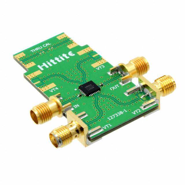
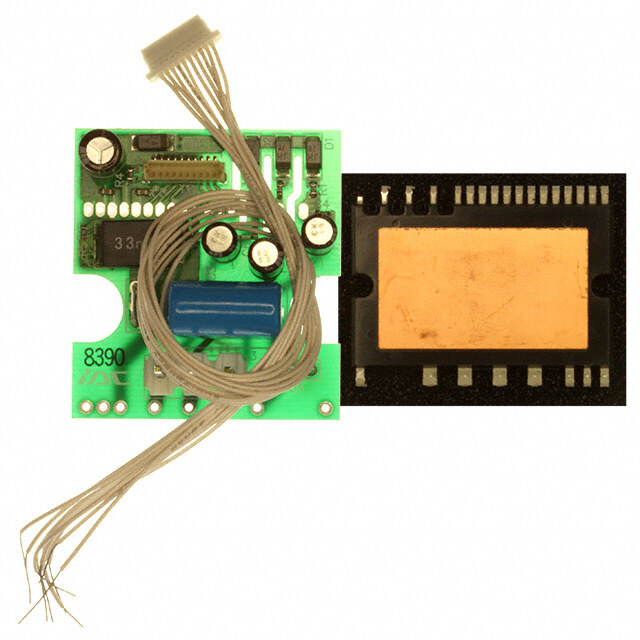
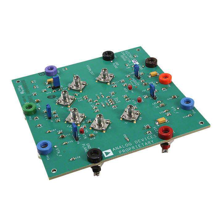
| 产品图片 |
|
| rohs | 符合RoHS无铅 / 符合限制有害物质指令(RoHS)规范要求 |
| 产品系列 | 模拟与数字IC开发工具,视频 IC 开发工具,Analog Devices EVAL-ADV7181DEBZ- |
| 数据手册 | |
| 产品型号 | EVAL-ADV7181DEBZ |
| 主要属性 | NTSC/PAL/SECAM 数字视频解码器 |
| 主要用途 | 视频,视频解码器 |
| 产品 | Evaluation Boards |
| 产品种类 | 视频 IC 开发工具 |
| 使用的IC/零件 | ADV7181D |
| 其它名称 | EVALADV7181DEBZ |
| 商标 | Analog Devices |
| 封装 | Bulk |
| 嵌入式 | 否 |
| 工作电源电压 | 7 V |
| 工具用于评估 | ADV7181 |
| 工厂包装数量 | 1 |
| 所含物品 | 板 |
| 接口类型 | HDMI, USB, Video |
| 描述/功能 | Evaluation board for the ADV7181 |
| 标准包装 | 1 |
| 用于 | ADV7181 |
| 类型 | Video Encoder |
| 辅助属性 | RGB 图形数字化仪 |


PDF Datasheet 数据手册内容提取
10-Bit, 10-Channel, Multiformat SDTV/HDTV Video Decoder and RGB Graphics Digitizer Data Sheet ADV7181D FEATURES GENERAL DESCRIPTION Four 10-bit ADCs sampling up to 75 MHz The ADV7181D is a high quality, single-chip, multiformat video 10 analog input channels decoder and graphics digitizer. This multiformat decoder supports SCART fast blank support the conversion of PAL, NTSC, and SECAM standards in the form Internal antialiasing filters of composite or S-Video into a digital ITU-R BT.656 format. NTSC, PAL, and SECAM color standards supported The ADV7181D also supports the decoding of a component 525p/625p component progressive scan supported RGB/YPrPb video signal into a digital YCrCb or RGB pixel 720p/1080i component HDTV supported output stream. Support for component video includes standards Digitizes RGB graphics up to 1024 × 768 at 70 Hz (XGA) such as 525i, 625i, 525p, 625p, 720p, 1080i, and many other HD 3 × 3 color space conversion matrix and SMPTE standards. Industrial temperature range: −40°C to +85°C 12-bit 4:4:4 DDR, 8-/10-/16-/20-bit SDR pixel output interface Graphics digitization is also supported by the ADV7181D; it is Programmable interrupt request output pin capable of digitizing RGB graphics signals from VGA to XGA Small package rates and converting them into a digital DDR RGB or YCrCb Low pin count pixel output stream. SCART and overlay functionality are enabled Single front end for video and graphics by the ability of the ADV7181D to simultaneously process CVBS VBI data slicer (including teletext) and standard definition RGB signals. The mixing of these signals Qualified for automotive applications is controlled by the fast blank (FB) pin. APPLICATIONS The ADV7181D contains two main processing sections. The first section is the standard definition processor (SDP), which Automotive entertainment processes all PAL, NTSC, and SECAM signal types. The second HDTVs section is the component processor (CP), which processes YPrPb LCD/DLP® projectors and RGB component formats, including RGB graphics. HDTV STBs with PVR DVD recorders with progressive scan input support The ADV7181D has unique software and hardware configuration AVR receivers requirements. For more information, see the Typical Connection Diagram section. Rev. B Document Feedback Information furnished by Analog Devices is believed to be accurate and reliable. However, no responsibility is assumed by Analog Devices for its use, nor for any infringements of patents or other One Technology Way, P.O. Box 9106, Norwood, MA 02062-9106, U.S.A. rights of third parties that may result from its use. Specifications subject to change without notice. No license is granted by implication or otherwise under any patent or patent rights of Analog Devices. Tel: 781.329.4700 ©2011–2017 Analog Devices, Inc. All rights reserved. Trademarks and registered trademarks are the property of their respective owners. Technical Support www.analog.com
ADV7181D Data Sheet TABLE OF CONTENTS Features .............................................................................................. 1 Standard Definition Processor (SDP) Pixel Data Output Applications ....................................................................................... 1 Modes ........................................................................................... 12 General Description ......................................................................... 1 Component Processor (CP) Pixel Data Output Modes ........ 12 Revision History ............................................................................... 2 Composite and S-Video Processing ......................................... 12 Functional Block Diagram .............................................................. 3 Component Video Processing .................................................. 13 Specifications ..................................................................................... 4 RGB Graphics Processing ......................................................... 13 Electrical Characteristics ............................................................. 4 General Features ......................................................................... 13 Video Specifications ..................................................................... 5 Detailed Descriptions .................................................................... 14 Analog Specifications ................................................................... 6 Analog Front End ....................................................................... 14 Timing Characteristics ................................................................ 7 Standard Definition Processor (SDP) ...................................... 14 Absolute Maximum Ratings ............................................................ 9 Component Processor (CP) ...................................................... 14 Reflow Solder ................................................................................ 9 Analog Input Muxing ................................................................ 15 Package Thermal Performance ................................................... 9 Pixel Output Formatting................................................................ 18 Thermal Resistance ...................................................................... 9 Recommended External Loop Filter Components .................... 19 ESD Caution .................................................................................. 9 Typical Connection Diagram........................................................ 20 Pin Configuration and Function Descriptions ........................... 10 Outline Dimensions ....................................................................... 21 Functional Overview ...................................................................... 12 Ordering Guide .......................................................................... 21 Analog Front End ....................................................................... 12 Automotive Products ................................................................. 21 REVISION HISTORY 6/2017—Rev. A to Rev. B Changes to Table 4 ............................................................................ 7 Changes to Figure 6 ........................................................................ 10 Changes to Table 8 .......................................................................... 16 12/2012—Rev. 0 to Rev. A Changes to General Description Section ...................................... 1 Change to Typical Connection Diagram Section ....................... 20 Updated Outline Dimensions ....................................................... 21 12/2011—Revision 0: Initial Version Rev. B | Page 2 of 24
Data Sheet ADV7181D FUNCTIONAL BLOCK DIAGRAM 100-49990 T E U D O PIXELDATA P19TOP10 P9TOP0 HS/CS VS FIELD/ LLC SFL/SYNC_ INT 0 0 1 1 RETTAMROF DNAOFIF TUPTUO 20 20 ERY FASTBLANKOVERLAYCONTROLANDAV CODEINSERTION AV CODEINSERTION V CO Y Cr Cb FB Y Cr Cb E ON PROCESSOR DARDVBI DATA RTECTION LUMALUMA2D COMBRESAMPLE(5H MAX) RESAMPLECONTROL CHROMACHROMA2D COMBRESAMPLE(4H MAX) T PROCESSOR CGMS DATAEXTRACTION OFFSETCONTROL DARD DEFINITI STANAUTODE LUMAFILTER SYNCEXTRACT CHROMAFILTER COMPONEN MACROVISIONDETECTION GAINCONTROL N A T N S ON K MACROVISIDETECTIO S/Y fSCECOVERY CHROMADEMOD ACTIVE PEAANDAGC DIGITALFINECLAMP B R V C VBS C Cr Cb 10 10 10 C PACESION 10 10 10 10 R SER DATAREPROCESSOR DECIMATIONANDOWNSAMPLINGFILTERS COLO CONV P D 0 0 0 0 1 1 1 1 0 1 2 3 C C C C D D D D A A A A D ANTI-CLAMPALIASINGFILTER ANTI-CLAMPALIASINGFILTERINPUTMUXANTI-CLAMPALIASINGFILTER ANTI-CLAMPALIASINGFILTER SERIAL INTERFACECONTROLAND VBI DATA SYNC PROCESSINGANDCLOCK GENERATION SSPDSTDI XTALXTAL1 1 ADV718 A110INTO10AIN CVBSS-VIDEOYPrPbSCART–B + CVBS)HICS RGB FB SCLK SDATA ALSB HS_IN/CS_INVS_IN SOGSOY GP RA (R G Figure 1. Rev. B | Page 3 of 24
ADV7181D Data Sheet SPECIFICATIONS ELECTRICAL CHARACTERISTICS AVDD = 3.15 V to 3.45 V, DVDD = 1.65 V to 2.0 V, DVDDIO = 3.0 V to 3.6 V, PVDD = 1.71 V to 1.89 V, nominal input range = 1.6 V. T MIN to T = −40°C to +85°C, unless otherwise noted. The minimum and maximum specifications are guaranteed over this temperature range. MAX Table 1. Parameter1 Symbol Test Conditions/Comments Min Typ Max Unit STATIC PERFORMANCE2, 3 Resolution (Each ADC) N 10 Bits Integral Nonlinearity INL BSL at 27 MHz (10-bit level) ±0.6 ±2.5 LSB BSL at 54 MHz (10-bit level) −0.6/+0.7 LSB BSL at 74 MHz (10-bit level) ±1.4 LSB Differential Nonlinearity DNL At 27 MHz (10-bit level) −0.2/+0.25 −0.99/+2.5 LSB At 54 MHz (10-bit level) −0.2/+0.25 LSB At 74 MHz (10-bit level) ±0.9 LSB DIGITAL INPUTS Input High Voltage4 V 2 V IH HS_IN, VS_IN low trigger mode 0.7 V Input Low Voltage5 V 0.8 V IL HS_IN, VS_IN low trigger mode 0.3 V Input Current I −10 +10 µA IN Input Capacitance6 C 10 pF IN DIGITAL OUTPUTS Output High Voltage7 V I = 0.4 mA 2.4 V OH SOURCE Output Low Voltage7 V I = 3.2 mA 0.4 V OL SINK High Impedance Leakage Current I Pin 1 60 µA LEAK All other output pins 10 µA Output Capacitance6 C 20 pF OUT POWER REQUIREMENTS6 Digital Core Power Supply DVDD 1.65 1.8 2.0 V Digital I/O Power Supply DVDDIO 3.0 3.3 3.6 V PLL Power Supply PVDD 1.71 1.8 1.89 V Analog Power Supply AVDD 3.15 3.3 3.45 V Digital Core Supply Current I CVBS input sampling at 54 MHz 105 mA DVDD Graphics RGB sampling at 75 MHz 90 mA SCART RGB FB sampling at 54 MHz 106 mA Digital I/O Supply Current I CVBS input sampling at 54 MHz 4 mA DVDDIO Graphics RGB sampling at 75 MHz 38 mA PLL Supply Current I CVBS input sampling at 54 MHz 11 mA PVDD Graphics RGB sampling at 75 MHz 12 mA Analog Supply Current8 I CVBS input sampling at 54 MHz 99 mA AVDD Graphics RGB sampling at 75 MHz 166 mA SCART RGB FB sampling at 54 MHz 200 mA Power-Down Current I 2.25 mA PWRDN Green Mode Power-Down I Synchronization bypass function 16 mA PWRDNG Power-Up Time t 20 ms PWRUP 1 All specifications are obtained using the Analog Devices, Inc., recommended programming scripts. 2 All ADC linearity tests performed at input range of full scale − 12.5% and at zero scale + 12.5%. 3 Maximum INL and DNL specifications obtained with part configured for component video input. 4 To obtain specified VIH level on Pin 22, program Register 0x13 (WO) with a value of 0x04. If Register 0x13 is programmed with a value of 0x00, then VIH on Pin 22 is 1.2 V. 5 To obtain specified VIL level on Pin 22, program Register 0x13 (WO) with a value of 0x04. If Register 0x13 is programmed with a value of 0x00, then VIL on Pin 22 is 0.4 V. 6 Guaranteed by characterization. 7 VOH and VOL levels obtained using default drive strength value (0xD5) in Register Subaddress 0xF4. 8 For CVBS current measurements only, ADC0 is powered up. For RGB current measurements only, ADC0, ADC1, and ADC2 are powered up. For SCART FB current measurements, all four ADCs are powered up. Rev. B | Page 4 of 24
Data Sheet ADV7181D VIDEO SPECIFICATIONS AVDD = 3.15 V to 3.45 V, DVDD = 1.65 V to 2.0 V, DVDDIO = 3.0 V to 3.6 V, PVDD = 1.71 V to 1.89 V. T to T = −40°C to +85°C, MIN MAX unless otherwise noted. The minimum and maximum specifications are guaranteed over this temperature range. Table 2. Parameter1 Symbol Test Conditions/Comments Min Typ Max Unit NONLINEAR SPECIFICATIONS Differential Phase DP CVBS input, modulated 5 step 0.5 Degrees Differential Gain DG CVBS input, modulated 5 step 0.5 % Luma Nonlinearity LNL CVBS input, 5 step 0.5 % NOISE SPECIFICATIONS Signal-to-Noise Ratio, Unweighted SNR Luma ramp 54 56 dB Luma flat field 58 60 dB Analog Front-End Crosstalk 60 dB LOCK TIME SPECIFICATIONS Horizontal Lock Range −5 +5 % Vertical Lock Range 40 70 Hz f Subcarrier Lock Range ±1.3 kHz SC Color Lock-In Time 60 Lines Synchronization Depth Range2 20 200 % Color Burst Range 5 200 % Vertical Lock Time 2 Fields Horizontal Lock Time 100 Lines CHROMA SPECIFICATIONS Hue Accuracy 1 Degrees Color Saturation Accuracy CL_AC 1 % Color AGC Range 5 400 % Chroma Amplitude Error 0.5 % Chroma Phase Error 0.4 Degrees Chroma Luma Intermodulation 0.2 % LUMA SPECIFICATIONS Luma Brightness Accuracy CVBS, 1 V input 1 % Luma Contrast Accuracy CVBS, 1 V input 1 % 1 Guaranteed by characterization. 2 Nominal synchronization depth is 300 mV at 100% synchronization depth range. Rev. B | Page 5 of 24
ADV7181D Data Sheet ANALOG SPECIFICATIONS AVDD = 3.15 V to 3.45 V, DVDD = 1.65 V to 2.0 V, DVDDIO = 3.0 V to 3.6 V, PVDD = 1.71 V to 1.89 V. T to T = −40°C to +85°C, MIN MAX unless otherwise noted. The minimum and maximum specifications are guaranteed over this temperature range. The recommended analog input video signal range is 0.5 V to 1.6 V, typically 1 V p-p. Table 3. Parameter1 Test Conditions/Comments Min Typ Max Unit CLAMP CIRCUITRY External Clamp Capacitor 0.1 µF Input Impedance All Pins Except for Pin 32 (FB) Clamps switched off 10 MΩ Pin 32 (FB) 20 kΩ Common-Mode Level (CML) 1.86 V ADC Full-Scale Level CML + 0.8 V ADC Zero-Scale Level CML − 0.8 V ADC Dynamic Range 1.6 V Clamp Level (When Locked) CVBS input CML − 0.292 V SCART RGB input (R, G, B signals) CML − 0.4 V S-Video input (Y signal) CML − 0.292 V S-Video input (C signal) CML V Component input (Y, Pr, Pb signals) CML − 0.3 V PC RGB input (R, G, B signals) CML − 0.3 V Large Clamp Source Current SDP only 0.75 mA Large Clamp Sink Current SDP only 0.9 mA Fine Clamp Source Current SDP only 17 µA Fine Clamp Sink Current SDP only 17 µA 1 Guaranteed by characterization. Rev. B | Page 6 of 24
Data Sheet ADV7181D TIMING CHARACTERISTICS AVDD = 3.15 V to 3.45 V, DVDD = 1.65 V to 2.0 V, DVDDIO = 3.0 V to 3.6 V, PVDD = 1.71 V to 1.89 V. T to T = −40°C to +85°C, MIN MAX unless otherwise noted. The minimum and maximum specifications are guaranteed over this temperature range. Table 4. Parameter1 Symbol Description Min Typ Max Unit SYSTEM CLOCK AND CRYSTAL Crystal Nominal Frequency 28.63636 MHz Crystal Frequency Stability ±50 ppm Horizontal Sync Input Frequency 14.8 110 kHz LLC Frequency Range 12.825 75 MHz I2C PORT2 SCLK Frequency 400 kHz SCLK Minimum Pulse Width High t 0.6 μs 1 SCLK Minimum Pulse Width Low t 1.3 μs 2 Hold Time (Start Condition) t 0.6 μs 3 Setup Time (Start Condition) t 0.6 μs 4 SDATA Setup Time t 100 ns 5 SCLK and SDATA Rise Time t 300 ns 6 SCLK and SDATA Fall Time t 300 ns 7 Setup Time (Stop Condition) t 0.6 μs 8 RESET FEATURE Reset Pulse Width 5 ms CLOCK OUTPUTS LLC Mark-Space Ratio t:t 45:55 55:45 % duty 9 10 cycle DATA AND CONTROL OUTPUTS Data Output Transition Time SDR (SDP)3 t Negative clock edge to start of valid data 3.6 ns 11 t End of valid data to negative clock edge 2.4 ns 12 SDR (CP)4 t End of valid data to negative clock edge 2.8 ns 13 t Negative clock edge to start of valid data 0.1 ns 14 DDR (CP)4, 5 t Positive clock edge to end of valid data 1.9 ns 15 t Start of valid data to positive clock edge 1.7 ns 16 t Negative clock edge to end of valid data 1.4 ns 17 t Start of valid data to negative clock edge 1.7 ns 18 1 Guaranteed by characterization. 2 TTL input values are 0 V to 3 V, with rise/fall times of ≤3 ns, measured between the 10% and 90% points. 3 SDP timing figures obtained using default drive strength value (0xD5) in Register Subaddress 0xF4. 4 CP timing figures obtained using maximum drive strength value (0xFF) in Register Subaddress 0xF4. 5 Guaranteed by characterization up to 75 MHz pixel clock. Timing Diagrams t t t 3 5 3 SDATA t t 6 1 SCLK t2 t7 t4 t8 09994-002 Figure 2. I2C Timing Rev. B | Page 7 of 24
ADV7181D Data Sheet t9 t10 LLC t11 t12 HSSP/FC0LS/T,S OFY INPEC1L9_D,O/ DVUSET,, 09994-003 Figure 3. Pixel Port and Control SDR Output Timing (SDP Core) t9 t10 LLC t13 t14 P0TO P19 09994-004 Figure 4. Pixel Port and Control SDR Output Timing (CP Core) LLC t16 t18 P6TO P19 t15 t17 09994-005 Figure 5. Pixel Port and Control DDR Output Timing (CP Core) Rev. B | Page 8 of 24
Data Sheet ADV7181D ABSOLUTE MAXIMUM RATINGS PACKAGE THERMAL PERFORMANCE Table 5. Parameter Rating To reduce power consumption when using the part, turn off any AVDD to GND 4 V unused ADCs. DVDD to GND 2.2 V It is imperative that the recommended scripts be used for the PVDD to GND 2.2 V following high current modes: SCART, 720p, 1080i, and all DVDDIO to GND 4 V RGB graphic standards. Using the recommended scripts ensures DVDDIO to AVDD −0.3 V to +0.3 V correct thermal performance. These scripts are available from PVDD to DVDD −0.3 V to +0.3 V a local field applications engineer (FAE). DVDDIO to PVDD −0.3 V to +2 V The junction temperature must always stay below the maximum DVDDIO to DVDD −0.3 V to +2 V junction temperature (T ) of 125°C. The junction temperature AVDD to PVDD −0.3 V to +2 V JMAX can be calculated by AVDD to DVDD −0.3 V to +2 V Digital Inputs to GND GND − 0.3 V to TJ = TA MAX + (θJA × WMAX) DVDDIO + 0.3 V where: Digital Outputs to GND GND − 0.3 V to T = 85°C. DVDDIO + 0.3 V A MAX θ = 20.3°C/W. Analog Inputs to GND GND − 0.3 V to JA W = ((AVDD × I ) + (DVDD × I ) + AVDD + 0.3 V MAX AVDD DVDD (DVDDIO × I ) + (PVDD × I )) Operating Temperature Range −40°C to +85°C DVDDIO PVDD Maximum Junction Temperature (T ) 125°C J MAX Storage Temperature Range −65°C to +150°C THERMAL RESISTANCE Infrared Reflow, Soldering (20 sec) 260°C Table 6 specifies the typical values for the junction-to-ambient Stresses at or above those listed under Absolute Maximum thermal resistance (θ ) and the junction-to-case thermal resis- JA Ratings may cause permanent damage to the product. This is a tance (θ ) for an ADV7181D soldered on a 4-layer PCB with JC stress rating only; functional operation of the product at these solid ground plane. or any other conditions above those indicated in the operational section of this specification is not implied. Operation beyond Table 6. Thermal Resistance the maximum operating conditions for extended periods may Package Type θJA1 θJC Unit affect product reliability. 64-Lead LFCSP (CP-64-3) 20.3 1.2 °C/W REFLOW SOLDER 1 In still air. The ADV7181D is a Pb-free, environmentally friendly product. It is manufactured using the most up-to-date materials and pro- ESD CAUTION cesses. The coating on the leads of each device is 100% pure Sn electroplate. The device is suitable for Pb-free applications and can withstand surface-mount soldering at up to 255°C ± 5°C. In addition, the ADV7181D is backward-compatible with conventional SnPb soldering processes. This means that the electroplated Sn coating can be soldered with Sn/Pb solder pastes at conventional reflow temperatures of 220°C to 235°C. Rev. B | Page 9 of 24
ADV7181D Data Sheet PIN CONFIGURATION AND FUNCTION DESCRIPTIONS N _I E S VSFIELD/DP16P17P18P19DVDDGNDHS_IN/CVS_INSCLKSDATAALSBRESETSOYA10IN 4321098765432109 6666655555555554 INT 1 48 AIN9 HS/CS 2 47 AIN8 GND 3 46 AIN7 DVDDIO 4 45 AIN6 P15 5 44 CAPC2 P14 6 43 CML P13 7 42 REFOUT P12 8 ADV7181D 41 AVDD SFL/SYNC_OUT 9 TOP VIEW 40 CAPY2 GND10 (Not to Scale) 39 CAPY1 DVDDIO 11 38 AIN5 P1112 37 AIN4 P1013 36 AIN3 P914 35 AIN2 P815 34 AIN1 P716 33 SOG 7890123456789012 1112222222222333 654C1LDD3210NFDB PPPLLXTALXTADVDGNPPPPRDWELPPVDF W N1.OTTHEES EXPOSED PAD MUST BE CONNECTED TO GND. P 09994-006 Figure 6. Pin Configuration Table 7. Pin Function Descriptions Pin No. Mnemonic Type Description 1 INT Output Interrupt. This pin can be active low or active high. When SDP/CP status bits change, this pin is triggered. The set of events that triggers an interrupt is under user control. 2 HS/CS Output Horizontal Synchronization Output Signal (HS). Available in SDP and CP modes. Digital Composite Synchronization Signal (CS). Available in CP mode only. 3, 10, 24, 57 GND Ground Ground. 4, 11 DVDDIO Power Digital I/O Supply Voltage (3.3 V). 28 to 25, 19 to 12, P0 to P19 Output Video Pixel Output Port. See Table 10 and Table 11 for output configuration modes. 8 to 5, 62 to 59 9 SFL/SYNC_OUT Output Subcarrier Frequency Lock (SFL). This pin contains a serial output stream that can be used to lock the subcarrier frequency when this decoder is connected to any Analog Devices digital video encoder. Sliced Synchronization Output Signal (SYNC_OUT). Available in CP mode only. 20 LLC Output Line-Locked Clock Output for Pixel Data. The range is 12.825 MHz to 75 MHz. 21 XTAL1 Output This pin should be connected to the 28.63636 MHz crystal or left unconnected if an external 3.3 V, 28.63636 MHz clock oscillator source is used to clock the ADV7181D. In crystal mode, the crystal must be a fundamental crystal. 22 XTAL Input Input Pin for the 28.63636 MHz Crystal. This input can be overdriven by an external 3.3 V, 28.63636 MHz clock oscillator source to clock the ADV7181D. 23, 58 DVDD Power Digital Core Supply Voltage (1.8 V). 29 PWRDWN Input Power-Down Input. A Logic 0 on this pin places the ADV7181D in power-down mode. 30 ELPF Output External Loop Filter Output. The recommended external loop filter must be connected to this pin (see the Recommended External Loop Filter Components section). 31 PVDD Power PLL Supply Voltage (1.8 V). 32 FB Input Fast Blank Input. Fast switch between CVBS and RGB analog signals. 33 SOG Input Sync on Green Input. Used in embedded synchronization mode. 34 to 38, 45 to 49 A 1 to A 10 Input Analog Video Input Channels. IN IN 39, 40 CAPY1, CAPY2 Input ADC Capacitor Network. See Figure 9 for a recommended capacitor network for Rev. B | Page 10 of 24
Data Sheet ADV7181D Pin No. Mnemonic Type Description these pins. 41 AVDD Power Analog Supply Voltage (3.3 V). 42 REFOUT Output Internal Voltage Reference Output. See Figure 9 for a recommended capacitor network for this pin. 43 CML Output Common-Mode Level Pin for the Internal ADCs. See Figure 9 for a recommended capacitor network for this pin. 44 CAPC2 Input ADC Capacitor Network. See Figure 9 for a recommended capacitor network for this pin. 50 SOY Input Sync on Luma Input. Used in embedded synchronization mode. 51 RESET Input System Reset Input, Active Low. A minimum low reset pulse width of 5 ms is required to reset the ADV7181D circuitry. 52 ALSB Input This pin selects the I2C address for the ADV7181D control and VBI readback ports. When set to Logic 0, this pin sets the address for a write to Control Port 0x40 and the readback address for VBI Port 0x21. When set to Logic 1, this pin sets the address for a write to Control Port 0x42 and the readback address for VBI Port 0x23. 53 SDATA Input/ I2C Port Serial Data Input/Output Pin. Output 54 SCLK Input I2C Port Serial Clock Input. Maximum clock rate of 400 kHz. 55 VS_IN Input Vertical Synchronization Input Signal. This pin can be configured in CP mode to extract timing in a 5-wire mode. 56 HS_IN/CS_IN Input Horizontal Synchronization Input Signal (HS_IN). This pin can be configured in CP mode to extract timing in a 5-wire mode. Composite Synchronization Input Signal (CS_IN). This pin can be configured in CP mode to extract timing in a 4-wire mode. 63 FIELD/DE Output Field Synchronization Output Signal (FIELD). Used in all interlaced video modes. Data Enable Signal (DE). This pin can also be used as a data enable (DE) signal in CP mode to allow direct connection to an HDMI/DVI transmitter IC. 64 VS Output Vertical Synchronization Output Signal (SDP and CP Modes). EP Exposed Pad The exposed pad must be connected to GND. Rev. B | Page 11 of 24
ADV7181D Data Sheet FUNCTIONAL OVERVIEW This section provides a brief description of the functionality COMPOSITE AND S-VIDEO PROCESSING of the ADV7181D. For more information, see the Detailed Composite and S-Video processing features offer support for Descriptions section. NTSC M/J, NTSC 4.43, PAL B/D/I/G/H, PAL60, PAL M, PAL N, ANALOG FRONT END and SECAM (B, D, G, K, and L) standards in the form of CVBS and S-Video. Superadaptive, 2D, five-line comb filters for NTSC The analog front end of the ADV7181D contains four high and PAL provide superior chrominance and luminance separa- quality, 10-bit ADCs and a multiplexer (mux) with 10 analog tion for composite video. input channels to enable multisource connection without the requirement of an external multiplexer. The analog front end Composite and S-Video processing features also include full auto- also provides the following: matic detection and autoswitching of all worldwide standards (PAL, NTSC, and SECAM) and automatic gain control (AGC) • Four current and voltage clamp control loops to ensure with white peak mode to ensure that the video is always processed that dc offsets are removed from the video signal without loss of the video processing range. Other features include • SCART functionality and standard definition (SD) RGB overlay on CVBS controlled by the fast blank (FB) input • Adaptive Digital Line Length Tracking (ADLLT™), a • Four internal antialiasing filters to remove out-of-band proprietary architecture for locking to weak, noisy, and noise on standard definition input video signals unstable sources from VCRs and tuners • IF filter block to compensate for high frequency luma STANDARD DEFINITION PROCESSOR (SDP) attenuation due to tuner SAW filter PIXEL DATA OUTPUT MODES • Chroma transient improvement (CTI) The ADV7181D features the following SDP pixel data output • Luminance digital noise reduction (DNR) modes: • Color controls including hue, brightness, saturation, • 8-/10-bit ITU-R BT.656 4:2:2 YCrCb with embedded time contrast, and Cr and Cb offset controls codes and/or HS, VS, and FIELD • Certified Macrovision® copy protection detection on • 16-/20-bit 4:2:2 YCrCb with embedded time codes and/or composite and S-Video for all worldwide formats HS, VS, and FIELD (PAL/NTSC/SECAM) • 4× oversampling (54 MHz) for CVBS, S-Video, and COMPONENT PROCESSOR (CP) PIXEL DATA YUV modes OUTPUT MODES • Line-locked clock (LLC) output The ADV7181D features the following CP pixel data output • Letterbox detection support modes for single data rate (SDR) and double data rate (DDR): • Free-run output mode to provide stable timing when no • SDR 8-/10-bit 4:2:2 YCrCb for 525i and 625i video input is present • SDR 16-/20-bit 4:2:2 YCrCb for all standards • Vertical blanking interval (VBI) data processor, including • DDR 8-/10-bit 4:2:2 YCrCb for all standards teletext, video programming system (VPS), vertical interval • DDR 12-bit 4:4:4 RGB for graphics inputs time codes (VITC), closed captioning (CC), extended data service (XDS), wide screen signaling (WSS), copy genera- tion management system (CGMS), and compatibility with GemStar® 1×/2× electronic program guide • Clocked from a single 28.63636 MHz crystal • Subcarrier frequency lock (SFL) output for downstream video encoder • Differential gain, typically 0.5% • Differential phase, typically 0.5° Rev. B | Page 12 of 24
Data Sheet ADV7181D COMPONENT VIDEO PROCESSING GENERAL FEATURES Component video processing supports formats including 525i, The ADV7181D features HS/CS, VS, and FIELD/DE output 625i, 525p, 625p, 720p, 1080i, and many other HD formats, as signals with programmable position, polarity, and width, as well well as automatic adjustments that include gain (contrast) and as a programmable interrupt request output pin, INT, that signals offset (brightness), and manual adjustment controls. Other SDP/CP status changes. Other features include features supported by component video processing include • Low power consumption: 1.8 V digital core, 3.3 V analog • Analog component YPrPb/RGB video formats with and digital I/O, low power, power-down mode, and green embedded synchronization or with separate HS, VS, or CS PC mode • Color space conversion matrix to support YCrCb-to-DDR • Industrial temperature range of −40°C to +85°C RGB and RGB-to-YCrCb conversions • 64-lead, 9 mm × 9 mm, Pb-free LFCSP • Standard identification (STDI) to enable system level • 3.3 V ADCs giving enhanced dynamic range and component format detection performance • Synchronization source polarity detector (SSPD) to determine the source and polarity of the synchronization signals that accompany the input video • Certified Macrovision copy protection detection on component formats (525i, 625i, 525p, and 625p) • Free-run output mode to provide stable timing when no video input is present • Arbitrary pixel sampling support for nonstandard video sources RGB GRAPHICS PROCESSING RGB graphics processing offers a 75 MSPS conversion rate that supports RGB input resolutions up to 1024 × 768 at 70 Hz (XGA), automatic or manual clamp and gain controls for graphics modes, and contrast and brightness controls. Other features include • 32-phase DLL to allow optimum pixel clock sampling • Automatic detection of synchronization source and polarity by SSPD block • Standard identification enabled by the STDI block • RGB that can be color space converted to YCrCb and decimated to a 4:2:2 format for videocentric back-end IC interfacing • Data enable (DE) output signal supplied for direct connection to HDMI®/DVI transmitter IC • Arbitrary pixel sampling support for nonstandard video sources • RGB graphics supported on 12-bit DDR format Rev. B | Page 13 of 24
ADV7181D Data Sheet DETAILED DESCRIPTIONS ANALOG FRONT END The SDP also contains a chroma transient improvement (CTI) processor. This processor increases the edge rate on chroma The ADV7181D analog front end comprises four 10-bit ADCs transitions, resulting in a sharper video image. that digitize the analog video signal before applying it to the SDP or CP. The analog front end uses differential channels to each The SDP can process a variety of VBI data services, such as tele- ADC to ensure high performance in a mixed-signal application. text, closed captioning (CC), wide screen signaling (WSS), video programming system (VPS), vertical interval time codes (VITC), The front end also includes a 10-channel input mux that enables copy generation management system (CGMS), GemStar 1×/2×, multiple video signals to be applied to the ADV7181D. Current and extended data service (XDS). The ADV7181D SDP section has and voltage clamps are positioned in front of each ADC to ensure a Macrovision 7.1 detection circuit that allows it to detect Type I, that the video signal remains within the range of the converter. Type II, and Type III protection levels. The decoder is also fully Fine clamping of the video signals is performed downstream by robust to all Macrovision signal inputs. digital fine clamping in either the CP or SDP. COMPONENT PROCESSOR (CP) Optional antialiasing filters are positioned in front of each ADC. These filters can be used to band-limit standard definition video The CP section is capable of decoding and digitizing a wide range signals, removing spurious out-of-band noise. of component video formats in any color space. Component video standards supported by the CP are 525i, 625i, 525p, 625p, 720p, The ADCs are configured to run in 4× oversampling mode 1080i, graphics up to XGA at 70 Hz, and many other standards. when decoding composite and S-Video inputs; 2× oversampling is performed for component 525i, 625i, 525p, and 625p sources. The CP section of the ADV7181D contains an AGC block. All other video standards are 1× oversampled. Oversampling When no embedded synchronization is present, the video the video signals reduces the cost and complexity of external gain can be set manually. The AGC section is followed by a antialiasing filters with the benefit of an increased signal-to- digital clamp circuit, which ensures that the video signal is noise ratio (SNR). clamped to the correct blanking level. Automatic adjustments within the CP include gain (contrast) and offset (brightness); The ADV7181D can support simultaneous processing of CVBS manual adjustment controls are also supported. and RGB standard definition signals to enable SCART compati- bility and overlay functionality. A combination of CVBS and A fixed mode graphics RGB to component output is available. RGB inputs can be mixed and output under the control of the A color space conversion matrix is placed between the analog I2C registers and the fast blank (FB) pin. front end and the CP section. This enables YCrCb-to-DDR RGB STANDARD DEFINITION PROCESSOR (SDP) and RGB-to-YCrCb conversions. Many other standards of color space can be implemented using the color space converter. The SDP section is capable of decoding a large selection of baseband video signals in composite, S-Video, and YUV The output section of the CP is highly flexible. It can be config- formats. The video standards supported by the SDP include ured in SDR mode with one data packet per clock cycle or in PAL B/D/I/G/H, PAL60, PAL M, PAL N, NTSC M/J, NTSC 4.43, DDR mode where data is presented on the rising and falling and SECAM B/D/G/K/L. The ADV7181D automatically detects edges of the clock. In SDR and DDR modes, HS/CS, VS, and the video standard and processes it accordingly. FIELD/DE (where applicable) timing reference signals are provided. In SDR mode, a 20-bit 4:2:2 is possible. In DDR The SDP has a five-line, superadaptive, 2D comb filter that pro- mode, the ADV7181D can be configured in an 8-bit or 10-bit vides superior chrominance and luminance separation when 4:2:2 YCrCb or in a 12-bit 4:4:4 RGB pixel output interface with decoding a composite video signal. This highly adaptive filter corresponding timing signals. automatically adjusts its processing mode according to video standards and signal quality with no user intervention required. The CP section contains circuitry to enable the detection of The SDP has an IF filter block that compensates for attenuation Macrovision encoded YPrPb signals for 525i, 625i, 525p, and in the high frequency luma spectrum due to the tuner SAW filter. 625p. It is designed to be fully robust when decoding these types of signals. The SDP has specific luminance and chrominance parameter control for brightness, contrast, saturation, and hue. VBI extraction of component data is performed by the CP section of the ADV7181D for interlaced, progressive, and high The ADV7181D implements a patented ADLLT algorithm to definition scanning rates. The data extracted can be read back track varying video line lengths from sources such as a VCR. over the I2C interface. ADLLT enables the ADV7181D to track and decode poor quality video sources such as VCRs, noisy sources from tuner outputs, VCD players, and camcorders. Rev. B | Page 14 of 24
Data Sheet ADV7181D ANALOG INPUT MUXING The ADV7181D has an integrated analog muxing section, which allows more than one source of video signal to be connected to the decoder. Figure 7 outlines the overall structure of the input muxing provided in the ADV7181D. 0 ADC_SW_MAN_EN 1 2 3 4 5 6 7 8 9 1 N N N N N N N N N N AI AI AI AI AI AI AI AI AI AI AIN1 1 ADC0_SW[3:0] AIN2 AIN3 AIN4 AIN5 ADC0 AIN6 AIN7 AIN8 AIN9 AIN10 AIN4 AIN5 1 ADC1_SW[3:0] AIN6 AIN7 AIN8 ADC1 AIN9 AIN10 AIN3 1 ADC2_SW[3:0] AIN6 AIN7 AIN8 ADC2 AIN9 AIN10 1 ADC3_SW[3:0] AIN1 AIN6 ADC3 09994-007 Figure 7. Internal Pin Connections Rev. B | Page 15 of 24
ADV7181D Data Sheet Table 8 provides the recommended ADC mapping for the ADV7181D. Table 8. Recommended ADC Mapping Mode Required ADC Mapping Analog Input Channel Core Configuration1 CVBS ADC0 CVBS = A 1 SDP INSEL[3:0] = 1011 IN SDM_SEL[1:0] = 00 PRIM_MODE[3:0] = 0000 VID_STD[3:0] = 0010 YC/YC Auto Y = ADC0 Y = A 7 (set by manual SDP INSEL[3:0] = 0000 IN muxing, see Table 9) C = ADC1 C = A 9 (set by manual SDM_SEL[1:0] = 11 IN muxing, see Table 9) PRIM_MODE[3:0] = 0000 VID_STD[3:0] = 0010 Component YUV Y = ADC0 Y = A 10 (set by manual SDP INSEL[3:0] = 1001 IN muxing, see Table 9) U = ADC2 U = A 8 (set by manual SDM_SEL[1:0] = 00 IN muxing, see Table 9) V = ADC1 V = A 6 (set by manual PRIM_MODE[3:0] = 0000 IN muxing, see Table 9) VID_STD[3:0] = 0010 Component YUV Y = ADC0 Y = A 10 (set by manual CP INSEL[3:0] = 0000 IN muxing, see Table 9) U = ADC2 U = A 8 (set by manual SDM_SEL[1:0] = 00 IN muxing, see Table 9) V = ADC1 V = A 6 (set by manual PRIM_MODE[3:0] = 0000 IN muxing, see Table 9) VID_STD[3:0] = 1010 SCART RGB CBVS = ADC0 CVBS = A 4 (set by SDP INSEL[3:0] = 0000 IN manual muxing. see Table 9) G = ADC1 G = A 10 (set by manual SDM_SEL[1:0] = 00 IN muxing. see Table 9) B = ADC3 B = A 6 (set by manual PRIM_MODE[3:0] = 0000 IN muxing. see Table 9) R = ADC2 R = A 8 (set by manual VID_STD[3:0] = 00002 IN muxing. see Table 9) Graphics G = ADC0 G = A 2 (set by manual CP INSEL[3:0] = 0000 IN RGB Mode muxing, see Table 9) B = ADC2 B = A 3 (set by manual SDM_SEL[1:0] = 00 IN muxing, see Table 9) R = ADC1 R = A 5 (set by manual PRIM_MODE[3:0] = 0010 IN muxing, see Table 9) VID_STD[3:0] = 1100 1 Configuration to format follow-on blocks in correct frame. 2 Recommended VID_STD[3:0] setting for optimal thermal performance in SCART RGB mode. Rev. B | Page 16 of 24
Data Sheet ADV7181D The analog input muxes of the ADV7181D must be controlled Table 9 explains the ADC mapping configuration for the following: directly. This is referred to as manual input muxing. The manual • ADC_SW_MAN_EN, manual input muxing enable, muxing is activated by setting the ADC_SW_MAN_EN bit (see IO map, Address C4[7] Table 9). It affects only the analog switches in front of the ADCs. • ADC0_SW[3:0], ADC0 mux configuration, IO map, The INSEL, SDM_SEL, PRIM_MODE, and VID_STD bits must Address C3[3:0] still be set so that the follow-on blocks process the video data in • ADC1_SW[3:0], ADC1 mux configuration, IO map, the correct format. Address C3[7:4] Not every input pin can be routed to any ADC. The analog • ADC2_SW[3:0], ADC2 mux configuration, IO map, signal routing inside the IC imposes restrictions on the channel Address C4[3:0] routing. See Table 9 for an overview of the routing capabilities • ADC3_SW[3:0], ADC3 mux configuration, IO map, inside the chip. The four mux sections can be controlled by the Address F3[7:4] reserved control signal buses ADC0_SW[3:0], ADC1_SW[3:0], ADC2_SW[3:0], and ADC3_SW[3:0]. Table 9. Manual MUX Settings for All ADCs ADC_SW_MAN_EN = 1 ADC0 ADC1 ADC2 ADC3 ADC0_SW[3:0] Connection ADC1_SW[3:0] Connection ADC2_SW[3:0] Connection ADC3_SW[3:0] Connection 0000 N/A 0000 N/A 0000 N/A 0000 N/A 0001 A 2 0001 N/A 0001 N/A 0001 N/A IN 0010 A 3 0010 N/A 0010 A 3 0010 N/A IN IN 0011 A 5 0011 A 5 0011 N/A 0011 N/A IN IN 0100 A 6 0100 A 6 0100 A 6 0100 A 6 IN IN IN IN 0101 A 8 0101 A 8 0101 A 8 0101 N/A IN IN IN 0110 A 10 0110 A 10 0110 A 10 0110 N/A IN IN IN 0111 N/A 0111 N/A 0111 N/A 0111 N/A 1000 N/A 1000 N/A 1000 N/A 1000 N/A 1001 A 1 1001 N/A 1001 N/A 1001 A 1 IN IN 1010 N/A 1010 N/A 1010 N/A 1010 N/A 1011 A 4 1011 A 4 1011 N/A 1011 N/A IN IN 1100 N/A 1100 N/A 1100 N/A 1100 N/A 1101 A 7 1101 A 7 1101 A 7 1101 N/A IN IN IN 1110 A 9 1110 A 9 1110 A 9 1110 N/A IN IN IN 1111 N/A 1111 N/A 1111 N/A 1111 N/A Rev. B | Page 17 of 24
ADV7181D Data Sheet PIXEL OUTPUT FORMATTING Table 10. SDP Output Formats—SDR 4:2:2 (8-/10-/16-/20-Bit) 8-Bit SDR 10-Bit SDR Pixel Output Pin ITU-R BT.656 ITU-R BT.656 16-Bit SDR 20-Bit SDR P19 Y7, Cb7, Cr7 Y9, Cb9, Cr9 Y7 Y9 P18 Y6, Cb6, Cr6 Y8, Cb8, Cr8 Y6 Y8 P17 Y5, Cb5, Cr5 Y7, Cb7, Cr7 Y5 Y7 P16 Y4, Cb4, Cr4 Y6, Cb6, Cr6 Y4 Y6 P15 Y3, Cb3, Cr3 Y5, Cb5, Cr5 Y3 Y5 P14 Y2, Cb2, Cr2 Y4, Cb4, Cr4 Y2 Y4 P13 Y1, Cb1, Cr1 Y3, Cb3, Cr3 Y1 Y3 P12 Y0, Cb0, Cr0 Y2, Cb2, Cr2 Y0 Y2 P11 High-Z Y1, Cb1, Cr1 High-Z Y1 P10 High-Z Y0, Cb0, Cr0 High-Z Y0 P9 High-Z High-Z Cb7, Cr7 Cb9, Cr9 P8 High-Z High-Z Cb6, Cr6 Cb8, Cr8 P7 High-Z High-Z Cb5, Cr5 Cb7, Cr7 P6 High-Z High-Z Cb4, Cr4 Cb6, Cr6 P5 High-Z High-Z Cb3, Cr3 Cb5, Cr5 P4 High-Z High-Z Cb2, Cr2 Cb4, Cr4 P3 High-Z High-Z Cb1, Cr1 Cb3, Cr3 P2 High-Z High-Z Cb0, Cr0 Cb2, Cr2 P1 High-Z High-Z High-Z Cb1, Cr1 P0 High-Z High-Z High-Z Cb0, Cr0 Table 11. CP Output Formats—SDR 4:2:2 (16-/20-Bit) and DDR 4:4:4 (12-Bit) SDR 4:2:2 12-Bit DDR 4:4:41 Pixel Output 16-Bit SDR 20-Bit SDR Clock Rise Clock Fall P19 Y7 Y9 B7-0 R3-1 P18 Y6 Y8 B6-0 R2-1 P17 Y5 Y7 B5-0 R1-1 P16 Y4 Y6 B4-0 R0-1 P15 Y3 Y5 B3-0 G7-1 P14 Y2 Y4 B2-0 G6-1 P13 Y1 Y3 B1-0 G5-1 P12 Y0 Y2 B0-0 G4-1 P11 High-Z Y1 High-Z High-Z P10 High-Z Y0 High-Z High-Z P9 Cb7, Cr7 Cb9, Cr9 G3-0 R7-1 P8 Cb6, Cr6 Cb8, Cr8 G2-0 R6-1 P7 Cb5, Cr5 Cb7, Cr7 G1-0 R5-1 P6 Cb4, Cr4 Cb6, Cr6 G0-0 R4-1 P5 Cb3, Cr3 Cb5, Cr5 High-Z High-Z P4 Cb2, Cr2 Cb4, Cr4 High-Z High-Z P3 Cb1, Cr1 Cb3, Cr3 High-Z High-Z P2 Cb0, Cr0 Cb2, Cr2 High-Z High-Z P1 High-Z Cb1, Cr1 High-Z High-Z P0 High-Z Cb0, Cr0 High-Z High-Z 1 xx-0 corresponds to data clocked at the rising edge; xx-1 corresponds to data clocked at the falling edge. Rev. B | Page 18 of 24
Data Sheet ADV7181D RECOMMENDED EXTERNAL LOOP FILTER COMPONENTS The external loop filter components for the ELPF pin should be placed as close to the pin as possible. Figure 8 shows the recommended component values. ELPF 30 1.69kΩ 10nF 82nF PVDD = 1.8V 09994-008 Figure 8. ELPF Components Rev. B | Page 19 of 24
ADV7181D Data Sheet TYPICAL CONNECTION DIAGRAM For the latest software configuration files, visit the ADV7181D design support files Web page on the EngineerZone video forum. 900-49990 Figure 9. Typical Connection Rev. B | Page 20 of 24
Data Sheet ADV7181D OUTLINE DIMENSIONS 9.10 9.00 SQ 0.60 MAX 8.90 0.60 MAX PIN 1 INDICATOR 49 64 1 48 PIN 1 INDICATOR 8.85 0.50 EXPOSED 7.25 8.75 SQ BSC PAD 7.10 SQ 8.65 6.95 0.50 0.40 3332 1716 0.30 TOP VIEW BOTTOM VIEW 0.25 MIN 7.50 REF 1.00 12° MAX 0.80 MAX 0.65 TYP 0.85 0.05 MAX FOR PROPER CONNECTION OF 0.80 0.02 NOM THE EXPOSED PAD, REFER TO THE PIN CONFIGURATION AND SEATING 0.30 FUNCTION DESCRIPTIONS PLANE 0.23 0.20 REF SECTION OF THIS DATA SHEET. 0.18COMPLIANT TO JEDEC STANDARDS MO-220-VMMD-4 06-13-2012-C Figure 10. 64-Lead Lead Frame Chip Scale Package [LFCSP_VQ] 9 mm × 9 mm Body, Very Thin Quad (CP-64-3) Dimensions shown in millimeters ORDERING GUIDE Model1, 2 Temperature Range Package Description Package Option ADV7181DBCPZ −40°C to +85°C 64-Lead LFCSP CP-64-3 ADV7181DBCPZ-RL −40°C to +85°C 64-Lead LFCSP CP-64-3 ADV7181DWBCPZ −40°C to +85°C 64-Lead LFCSP CP-64-3 ADV7181DWBCPZ-RL −40°C to +85°C 64-Lead LFCSP CP-64-3 EVAL-ADV7181DEBZ Evaluation Board 1 Z = RoHS Compliant Part. 2 W = Qualified for Automotive Applications. AUTOMOTIVE PRODUCTS The ADV7181DW models are available with controlled manufacturing to support the quality and reliability requirements of automotive applications. Note that these automotive models may have specifications that differ from the commercial models; therefore, designers should review the Specifications section of this data sheet carefully. Only the automotive grade products shown are available for use in automotive applications. Contact your local Analog Devices account representative for specific product ordering information and to obtain the specific Automotive Reliability reports for these models. Rev. B | Page 21 of 24
ADV7181D Data Sheet NOTES Rev. B | Page 22 of 24
Data Sheet ADV7181D NOTES Rev. B | Page 23 of 24
ADV7181D Data Sheet NOTES I2C refers to a communications protocol originally developed by Philips Semiconductors (now NXP Semiconductors). ©2011–2017 Analog Devices, Inc. All rights reserved. Trademarks and registered trademarks are the property of their respective owners. D09994-0-6/17(B) Rev. B | Page 24 of 24