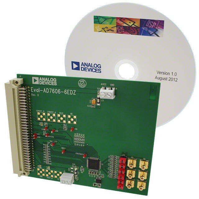
ICGOO在线商城 > 开发板,套件,编程器 > 评估板 - 模数转换器(ADC) > EVAL-AD7799EBZ
 Datasheet下载
- 型号: EVAL-AD7799EBZ
- 制造商: Analog
- 库位|库存: xxxx|xxxx
- 要求:
| 数量阶梯 | 香港交货 | 国内含税 |
| +xxxx | $xxxx | ¥xxxx |
查看当月历史价格
查看今年历史价格
EVAL-AD7799EBZ产品简介:
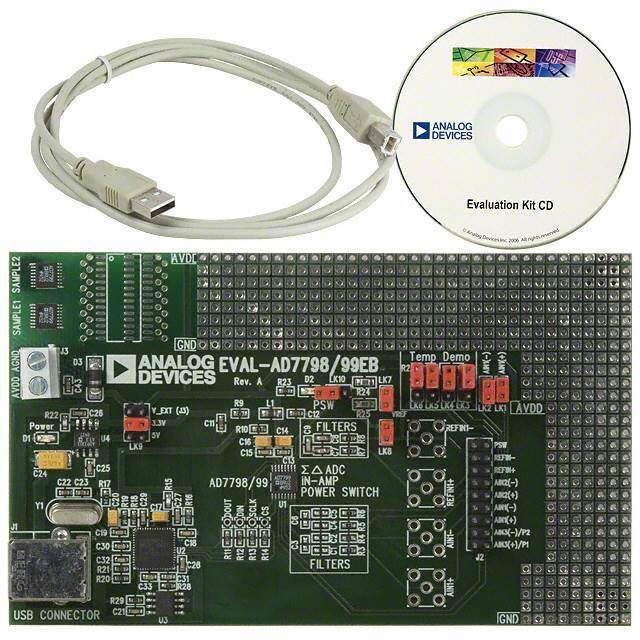
ICGOO电子元器件商城为您提供EVAL-AD7799EBZ由Analog设计生产,在icgoo商城现货销售,并且可以通过原厂、代理商等渠道进行代购。 EVAL-AD7799EBZ价格参考。AnalogEVAL-AD7799EBZ封装/规格:评估板 - 模数转换器(ADC), AD7799 - 24 Bit 470 Samples per Second Analog to Digital Converter (ADC) Evaluation Board。您可以下载EVAL-AD7799EBZ参考资料、Datasheet数据手册功能说明书,资料中有EVAL-AD7799EBZ 详细功能的应用电路图电压和使用方法及教程。
EVAL-AD7799EBZ 是由 Analog Devices Inc. 提供的一款评估板,用于评估 AD7799 模数转换器(ADC)。AD7799 是一款高性能、低功耗的 24 位 Σ-Δ ADC,广泛应用于需要高精度和低噪声性能的场景。以下是 EVAL-AD7799EBZ 的主要应用场景:

 1. 工业自动化与过程控制
   - 在工业自动化领域,EVAL-AD7799EBZ 可用于评估 AD7799 对传感器信号的精确采集能力。例如,压力传感器、温度传感器或流量传感器的输出信号可以通过 AD7799 转换为高精度数字信号,用于实时监控和控制。
   - 它适用于 PLC(可编程逻辑控制器)、数据采集系统(DAQ)以及工业仪表中。

 2. 医疗设备
   - 医疗设备对信号精度要求极高,EVAL-AD7799EBZ 可用于评估 AD7799 在心电图(ECG)、血压监测、血糖仪等设备中的表现。
   - 其低功耗特性也使其适合便携式医疗设备的设计。

 3. 能源管理
   - 在智能电网和能源管理系统中,EVAL-AD7799EBZ 可用于评估电力参数(如电压、电流)的高精度测量。
   - 它支持多通道输入,可以同时监测多个电源回路,适合电能表、功率分析仪等应用。

 4. 环境监测
   - 环境监测设备(如空气质量监测仪、水质分析仪)需要对微弱信号进行精确采集。EVAL-AD7799EBZ 可帮助开发人员评估 AD7799 在这些场景中的性能。
   - 其高分辨率和低噪声特性使其非常适合检测微小的环境变化。

 5. 消费电子
   - 在高端音频设备中,EVAL-AD7799EBZ 可用于评估 AD7799 对音频信号的数字化处理能力。
   - 它还可以用于家用健康设备(如体重秤、体脂分析仪)的开发,提供高精度的重量或阻抗测量。

 6. 科研与实验
   - 科研人员可以使用 EVAL-AD7799EBZ 进行高精度数据采集实验,例如物理量(如振动、应力)的测量。
   - 其灵活性和易用性使其成为实验室环境中理想的评估工具。

 特点总结:
- 高精度:24 位分辨率,适合对精度要求极高的应用。
- 低功耗:适合电池供电的便携式设备。
- 多通道输入:支持多个模拟信号的同时采集。
- 易于评估:评估板提供了完整的硬件和软件支持,便于快速开发和测试。

通过 EVAL-AD7799EBZ,工程师可以快速验证 AD7799 的性能,优化设计并缩短产品开发周期。
| 参数 | 数值 |
| ADC数 | 1 |
| 产品目录 | 编程器,开发系统嵌入式解决方案 |
| 描述 | BOARD EVALUATION FOR AD7799数据转换 IC 开发工具 EVAL BRD AD7799 |
| 产品分类 | 评估板 - 模数转换器 (ADC)工程工具 |
| 品牌 | Analog Devices |
| 产品手册 | |
| 产品图片 |
|
| rohs | 符合RoHS无铅 / 符合限制有害物质指令(RoHS)规范要求 |
| 产品系列 | 模拟与数字IC开发工具,数据转换 IC 开发工具,Analog Devices EVAL-AD7799EBZ- |
| 数据手册 | |
| 产品型号 | EVAL-AD7799EBZ |
| 不同条件下的功率(典型值) | 2.5mW @ 470SPS |
| 产品 | Evaluation Boards |
| 产品种类 | 数据转换 IC 开发工具 |
| 位数 | 24 |
| 使用的IC/零件 | AD7799 |
| 其它名称 | EVALAD7799EBZ |
| 商标 | Analog Devices |
| 封装 | Bulk |
| 工作温度 | -40°C ~ 105°C |
| 工作电源电压 | 2.7 V to 5.25 V |
| 工具用于评估 | AD7799 |
| 工厂包装数量 | 1 |
| 所含物品 | 板,线缆 |
| 接口类型 | SPI |
| 数据接口 | 串行 |
| 最大工作温度 | + 105 C |
| 最小工作温度 | - 40 C |
| 标准包装 | 1 |
| 相关产品 | /product-detail/zh/AD7799BRU-REEL/AD7799BRU-REEL-ND/760352/product-detail/zh/AD7799BRUZ-REEL/AD7799BRUZ-REELTR-ND/760351/product-detail/zh/AD7799BRUZ/AD7799BRUZ-ND/751090/product-detail/zh/AD7799BRU/AD7799BRU-ND/736083 |
| 类型 | ADC |
| 系列 | AD7799 |
| 输入范围 | ±VREF/增益 |
| 采样率(每秒) | 470 |


- 商务部:美国ITC正式对集成电路等产品启动337调查
- 曝三星4nm工艺存在良率问题 高通将骁龙8 Gen1或转产台积电
- 太阳诱电将投资9.5亿元在常州建新厂生产MLCC 预计2023年完工
- 英特尔发布欧洲新工厂建设计划 深化IDM 2.0 战略
- 台积电先进制程称霸业界 有大客户加持明年业绩稳了
- 达到5530亿美元!SIA预计今年全球半导体销售额将创下新高
- 英特尔拟将自动驾驶子公司Mobileye上市 估值或超500亿美元
- 三星加码芯片和SET,合并消费电子和移动部门,撤换高东真等 CEO
- 三星电子宣布重大人事变动 还合并消费电子和移动部门
- 海关总署:前11个月进口集成电路产品价值2.52万亿元 增长14.8%


PDF Datasheet 数据手册内容提取
3-Channel, Low Noise, Low Power, 16-/24-Bit, Σ-Δ ADC with On-Chip In-Amp Data Sheet AD7798/AD7799 FEATURES FUNCTIONAL BLOCK DIAGRAM RMS noise: GND AVDD REFIN(+)REFIN(–) 27 nV at 4.17 Hz (AD7799) REFERENCE 65 nV at 16.7 Hz (AD7799) AD7798/AD7799 DETECT 40 nV at 4.17 Hz (AD7798) 85 nV at 16.7 Hz (AD7798) AIN1(+) AVDD AIN1(–) Current: 380 µA typical AIN2(+) DOUT/RDY PLooww enro-disoew, pnr:o 1g µraAm mmaaxbimleu gma in, instrumentation amp AAIINNA33I((N+–))2//P(P–21) MUX IN-AMP AΣD-ΔC INCTSOEAENRNRTFDIRAAOLCLE DSCINLK LOGIC CS Update rate: 4.17 Hz to 470 Hz 3 differential inputs GND DVDD PSW INTERNAL AD7798: 16-BIT ISnimteurnltaaln celoocuks o5s0c Hillza/t6o0r H z rejection GND CLOCK AD7799: 24-BIT 04856-001 Figure 1. Reference detect Low-side power switch Programmable digital outputs GENERAL DESCRIPTION Burnout currents Power supply: 2.7 V to 5.25 V The AD7798/AD7799 are low power, low noise, complete –40°C to +105°C temperature range analog front ends for high precision measurement applications. Independent interface power supply The AD7798/AD7799 contains a low noise, 16-/24-bit ∑-∆ 16-lead TSSOP package ADC with three differential analog inputs. The on-chip, low noise instrumentation amplifier means that signals of small INTERFACE amplitude can be interfaced directly to the ADC. With a gain 3-wire serial setting of 64, the rms noise is 27 nV for the AD7799 and 40 nV SPI®, QSPI™, MICROWIRE™, and DSP compatible for the AD7798 when the update rate equals 4.17 Hz. Schmitt trigger on SCLK On-chip features include a low-side power switch, reference APPLICATIONS detect, programmable digital output pins, burnout currents, and an internal clock oscillator. The output data rate from the Weigh scales part is software-programmable and can be varied from 4.17 Hz Pressure measurement to 470 Hz. Strain gauge transducers Gas analysis The part operates with a power supply from 2.7 V to 5.25 V. Industrial process control The AD7798 consumes a current of 300 µA typical, whereas the Instrumentation AD7799 consumes 380 µA typical. Both devices are housed in a Portable instrumentation 16-lead TSSOP package. Blood analysis Smart transmitters Liquid/gas chromotography 6-digit DVM Rev. B Document Feedback Information furnished by Analog Devices is believed to be accurate and reliable. However, no responsibility is assumed by Analog Devices for its use, nor for any infringements of patents or other One Technology Way, P.O. Box 9106, Norwood, MA 02062-9106, U.S.A. rights of third parties that may result from its use. Specifications subject to change without notice. No license is granted by implication or otherwise under any patent or patent rights of Analog Devices. Tel: 781.329.4700 ©2005–2013 Analog Devices, Inc. All rights reserved. Trademarks and registered trademarks are the property of their respective owners. Technical Support www.analog.com
AD7798/AD7799 Data Sheet TABLE OF CONTENTS Features .............................................................................................. 1 IO Register................................................................................... 17 Interface ............................................................................................. 1 Offset Register ............................................................................ 17 Applications ....................................................................................... 1 Full-Scale Register ...................................................................... 17 Functional Block Diagram .............................................................. 1 ADC Circuit Information.............................................................. 18 General Description ......................................................................... 1 Overview ..................................................................................... 18 Revision History ............................................................................... 2 Digital Interface .......................................................................... 19 Specifications ..................................................................................... 3 Circuit Description......................................................................... 22 Timing Characteristics ..................................................................... 6 Analog Input Channel ............................................................... 22 Absolute Maximum Ratings ............................................................ 8 Instrumentation Amplifier........................................................ 22 ESD Caution .................................................................................. 8 Bipolar/Unipolar Configuration .............................................. 22 Pin Configuration and Function Descriptions ............................. 9 Data Output Coding .................................................................. 23 Output Noise and Resolution Specifications .............................. 10 Burnout Currents ....................................................................... 23 AD7798 ........................................................................................ 10 Reference ..................................................................................... 23 AD7799 ........................................................................................ 11 Reference Detect ......................................................................... 23 Typical Performance Characteristics ........................................... 12 Reset ............................................................................................. 23 On-Chip Registers .......................................................................... 13 AV Monitor ............................................................................. 24 DD Communication Register .......................................................... 13 Calibration................................................................................... 24 Status Register ............................................................................. 14 Grounding and Layout .............................................................. 25 Mode Register ............................................................................. 14 Applications Information .............................................................. 26 Configuration Register .............................................................. 16 Weigh Scales ................................................................................ 26 Data Register ............................................................................... 17 Outline Dimensions ....................................................................... 27 ID Register ................................................................................... 17 Ordering Guide .......................................................................... 27 REVISION HISTORY 7/13—Rev. A to Rev. B Changes to Table 3 ............................................................................ 8 Changes to Digital Interface Section ............................................ 19 Changes to Ordering Guide .......................................................... 27 3/07—Rev. 0 to Rev. A Updated Format .................................................................. Universal Changes to Specifications ................................................................ 3 Changes to Table 5 and Table 6 ..................................................... 10 Changes to Table 7 and Table 8 ..................................................... 11 Changes to Table 14 ........................................................................ 15 Changes to Ordering Guide .......................................................... 27 1/05—Revision 0: Initial Version Rev. B | Page 2 of 28
Data Sheet AD7798/AD7799 SPECIFICATIONS AV = 2.7 V to 5.25 V; DV = 2.7 V to 5.25 V; GND = 0 V; REFIN(+) = AV ; REFIN(−) = 0 V. All specifications T to T , unless DD DD DD MIN MAX otherwise noted. Table 1. Parameter AD7798B/AD7799B1 Unit Test Conditions/Comments ADC CHANNEL Output Update Rate 4.17 − 470 Hz nom No Missing Codes2 24 Bits min AD7799: f < 242 Hz ADC 16 Bits min AD7798 Resolution See Table 5 to Table 8 Output Noise and Update Rates See Table 5 to Table 8 Integral Nonlinearity ±15 ppm of FSR max Offset Error3 ±1 µV typ Offset Error Drift vs. Temperature4 ±10 nV/°C typ Full-Scale Error3, 5 ±10 µV typ Gain Drift vs. Temperature4 ±1 ppm/°C typ Power Supply Rejection 100 dB min AIN = 1 V/gain, gain ≥ 4 ANALOG INPUTS Differential Input Voltage Ranges ±V /gain V nom V = REFIN(+) – REFIN(–), gain = 1 to 128 REF REF Absolute AIN Voltage Limits2 Unbuffered Mode GND − 30 mV V min Gain = 1 or 2 AV + 30 mV V max DD Buffered Mode GND + 100 mV V min Gain = 1 or 2 AV – 100 mV V max DD In-Amp Active GND + 300 mV V min Gain = 4 to 128 AV − 1.1 V max DD Common-Mode Voltage, V 0.5 V min V = (AIN(+) + AIN(−))/2, gain = 4 to 128 CM CM Analog Input Current Buffered Mode or In-Amp Active Average Input Current2 ±1 nA max Gain = 1 or 2, update rate < 100 Hz ±250 pA max Gain = 4 to 128, update rate < 100 Hz ±1 nA max AIN3(+)/AIN3(−), update rate < 100 Hz Average Input Current Drift ±2 pA/°C typ Unbuffered Mode Gain = 1 or 2 Average Input Current ±400 nA/V typ Input current varies with input voltage Average Input Current Drift ±50 pA/V/°C typ Normal Mode Rejection2 @ 50 Hz, 60 Hz 65 dB min 80 dB typ, 50 ± 1 Hz, 60 ± 1 Hz (FS[3:0] = 1010)6 @ 50 Hz 80 dB min 90 dB typ, 50 ± 1 Hz (FS[3:0] = 1001)6 @ 60 Hz 90 dB min 100 dB typ, 60 ± 1 Hz (FS[3:0] = 1000)6 Common-Mode Rejection @ DC 100 dB min AIN = 1 V/gain, gain ≥ 4 @ 50 Hz, 60 Hz2 100 dB min 50 ± 1 Hz, 60 ± 1 Hz (FS[3:0] = 1010)6 @ 50 Hz, 60 Hz2 100 dB min 50 ± 1 Hz (FS[3:0] = 10016), 60 ± 1 Hz (FS[3:0] = 10006) Rev. B | Page 3 of 28
AD7798/AD7799 Data Sheet Parameter AD7798B/AD7799B1 Unit Test Conditions/Comments REFERENCE External REFIN Voltage 2.5 V nom REFIN = REFIN(+) − REFIN(−) Reference Voltage Range2 0.1 V min AV V max When V = AV , the differential input must be DD REF DD limited to (0.9 x V /gain) if the in-amp is active. REF Absolute REFIN Voltage Limits2 GND − 30 mV V min AV + 30 mV V max DD Average Reference Input Current 400 nA/V typ Average Reference Input Current Drift ±0.03 nA/V/°C typ Normal Mode Rejection Same as for analog inputs Common-Mode Rejection 100 dB typ Reference Detect Levels 0.3 V min 0.65 V max NOXREF bit active if V < 0.3 V REF LOW-SIDE POWER SWITCH R 7 Ω max AV = 5 V ON DD 9 Ω max AV = 3 V DD Allowable Current2 30 mA max Continuous current DIGITAL OUTPUTS (P1 and P2) Output High Voltage, V 2 AV − 0.6 V min AV = 3 V, I = 100 µA OH DD DD SOURCE Output Low Voltage, V 2 0.4 V max AV = 3 V, I = 100 µA OL DD SINK Output High Voltage, V 2 4 V min AV = 5 V, I = 200 µA OH DD SOURCE Output Low Voltage, V 2 0.4 V max AV = 5 V, I = 800 µA OL DD SINK INTERNAL CLOCK Frequency2 64 ± 3% kHz min/max LOGIC INPUTS CS2 Input Low Voltage, V 0.8 V max DV = 5 V INL DD 0.4 V max DV = 3 V DD Input High Voltage, V 2.0 V min DV = 3 V or 5 V INH DD SCLK and DIN (Schmitt-Triggered Input)2 V(+) 1.4/2 V min/max DV = 5 V T DD V(–) 0.8/1.7 V min/max DV = 5 V T DD V(+) – V(–) 0.1/0.17 V min/max DV = 5 V T T DD V(+) 0.9/2 V min/max DV = 3 V T DD V(–) 0.4/1.35 V min/max DV = 3 V T DD V(+) − V(–) 0.06/0.13 V min/max DV = 3 V T T DD Input Currents ±10 µA max V = DV or GND IN DD Input Capacitance 10 pF typ All digital inputs LOGIC OUTPUTS Output High Voltage, V 2 DV − 0.6 V min DV = 3 V, I = 100 µA OH DD DD SOURCE Output Low Voltage, V 2 0.4 V max DV = 3 V, I = 100 µA OL DD SINK Output High Voltage, V 2 4 V min DV = 5 V, I = 200 µA OH DD SOURCE Output Low Voltage, V 2 0.4 V max DV = 5 V, I = 1.6 mA OL DD SINK Floating-State Leakage Current ±10 µA max Floating-State Output Capacitance 10 pF typ Data Output Coding Offset binary Rev. B | Page 4 of 28
Data Sheet AD7798/AD7799 Parameter AD7798B/AD7799B1 Unit Test Conditions/Comments SYSTEM CALIBRATION2 Full-Scale Calibration Limit 1.05 × FS V max FS = Full-scale analog input. When V = AV , the REF DD differential input must be limited to (0.9 × V /gain) REF if the in-amp is active. Zero-Scale Calibration Limit −1.05 × FS V min Input Span 0.8 × FS V min 2.1 × FS V max POWER REQUIREMENTS7 Power Supply Voltage AV – GND 2.7/5.25 V min/max DD DV – GND 2.7/5.25 V min/max DD Power Supply Currents I Current 140 µA max Unbuffered mode, 110 µA typ @ AV = 3 V, DD DD 125 µA typ @ AV = 5 V DD 180 µA max Buffered mode, gain = 1 or 2, 130 µA typ @ AV = 3 V, DD 165 µA typ @ AV = 5 V DD 400 µA max AD7798: gain = 4 to 128, 300 µA typ @ AV = 3 V, DD 350 µA typ @ AV = 5 V DD 500 µA max AD7799: gain = 4 to 128, 380 µA typ @ AV = 3 V, DD 440 µA typ @ AV = 5 V DD I (Power-Down Mode) 1 µA max DD 1 Temperature range is –40°C to +105°C. At the 19.6 Hz and 39.2 Hz update rates, the INL, power supply rejection (PSR), common-mode rejection (CMR), and normal mode rejection (NMR) do not meet the data sheet specification if the voltage on the AIN(+) or AIN(−) pins exceeds AVDD − 1.6 V typically. When this voltage is exceeded, the INL, for example, is reduced to 18 ppm of FS typically and the PSR is reduced to 69 dB typically. Therefore, for guaranteed performance at these update rates, the absolute voltage on the analog input pins needs to be below AVDD − 1.6 V. 2 Specification is not production tested, but is supported by characterization data at initial product release. 3 Following a calibration, this error is in the order of the noise for the programmed gain and update rate selected. 4 Recalibration at any temperature removes these errors. 5 Full-scale error applies to both positive and negative full-scale and applies at the factory calibration conditions (AVDD = 4 V, gain = 1, TA = 25°C). 6 FS[3:0] are the four bits used in the mode register to select the output word rate. 7 Digital inputs equal to DVDD or GND. Rev. B | Page 5 of 28
AD7798/AD7799 Data Sheet TIMING CHARACTERISTICS AV = 2.7 V to 5.25 V, DV = 2.7 V to 5.25 V, GND = 0 V, Input Logic 0 = 0 V, Input Logic 1 = DV , unless otherwise noted. DD DD DD Table 2. Parameter1, 2 Limit at T , T (B Version) Unit Conditions/Comments MIN MAX t 100 ns min SCLK high pulse width 3 t 100 ns min SCLK low pulse width 4 Read Operation t1 0 ns min CS falling edge to DOUT/RDY active time 60 ns max DV = 4.75 V to 5.25 V DD 80 ns max DV = 2.7 V to 3.6 V DD t 3 0 ns min SCLK active edge to data valid delay4 2 60 ns max DV = 4.75 V to 5.25 V DD 80 ns max DV = 2.7 V to 3.6 V DD t55, 6 10 ns min Bus relinquish time after CS inactive edge 80 ns max t6 0 ns min SCLK inactive edge to CS inactive edge t7 10 ns min SCLK inactive edge to DOUT/RDY high Write Operation t8 0 ns min CS falling edge to SCLK active edge setup time4 t 30 ns min Data valid to SCLK edge setup time 9 t 25 ns min Data valid to SCLK edge hold time 10 t11 0 ns min CS rising edge to SCLK edge hold time 1 Sample tested during initial release to ensure compliance. All input signals are specified with tR = tF = 5 ns (10% to 90% of DVDD) and timed from a voltage level of 1.6 V. 2 See Figure 3 and Figure 4. 3 These times are measured with the load circuit of Figure 2 and defined as the time required for the output to cross the VOL or VOH limits. 4 SCLK active edge is the falling edge of SCLK. 5 These times are derived from the measured time taken by the data output to change 0.5 V when loaded with the circuit of Figure 2. The measured time is then extrapolated back to remove the effects of charging or discharging the 50 pF capacitor. This means that the times quoted in the timing characteristics are the true bus relinquish times of the part and, as such, are independent of external bus loading capacitances. 6 RDY returns high after a read of the ADC. In single-conversion mode and continuous-conversion mode, data can be reread, if required, while RDY is high, but care should be taken to ensure that subsequent reads do not occur close to the next output update. In continuous read mode, the digital word can be read only once. ISINK (1.6mA WITH DVDD = 5V, 100µA WITH DVDD = 3V) TO OUTPUT 1.6V PIN 50pF I1S0O0UµRAC WE (IT20H0 DµAV DWDI T= H3 VD)VDD = 5V, 04856-002 Figure 2. Load Circuit for Timing Characterization Rev. B | Page 6 of 28
Data Sheet AD7798/AD7799 CS (I) t1 t6 t5 DOUT/RDY (O) MSB LSB t2 t7 t3 SCLK (I) I = INPUT, O = OUTPUT t4 04856-003 Figure 3. Read Cycle Timing Diagram CS (I) t8 t11 SCLK (I) t9 t10 DIN (I) MSB LSB I = INPUTF, iOgu =r eO U4.T WPUrTite Cycle Timing Diagram 04856-004 Rev. B | Page 7 of 28
AD7798/AD7799 Data Sheet ABSOLUTE MAXIMUM RATINGS T = 25°C, unless otherwise noted. A Stresses above those listed under Absolute Maximum Ratings may cause permanent damage to the device. This is a stress Table 3. rating only; functional operation of the device at these or any Parameter Rating other conditions above those listed in the operational sections AV to GND −0.3 V to +7 V DD of this specification is not implied. Exposure to absolute DV to GND −0.3 V to +7 V DD maximum rating conditions for extended periods may affect Analog Input Voltage to GND −0.3 V to AV + 0.3 V DD device reliability. Reference Input Voltage to GND −0.3 V to AV + 0.3 V DD Digital Input Voltage to GND −0.3 V to DV + 0.3 V DD Digital Output Voltage to GND −0.3 V to DVDD + 0.3 V ESD CAUTION AIN/Digital Input Current 10 mA Operating Temperature Range −40°C to +105°C Storage Temperature Range −65°C to +150°C Maximum Junction Temperature 150°C TSSOP θ Thermal Impedance 128°C/W JA θ Thermal Impedance 14°C/W JC Lead Temperature, Soldering Reflow 260°C Rev. B | Page 8 of 28
Data Sheet AD7798/AD7799 PIN CONFIGURATION AND FUNCTION DESCRIPTIONS SCLK 1 16 DIN CS 2 15 DOUT/RDY AIN3(+)/P1 3 AD7798/ 14 DVDD AIN3(–)/P2 4 AD7799 13 AVDD AIN1(+) 5 TOP VIEW 12 GND (Not to Scale) AIN1(–) 6 11 PSW AIN2(+) 7 10 REFIN(–) AIN2(–) 8 9 REFIN(+) 04856-005 Figure 5. Pin Configuration Table 4. Pin Function Descriptions Pin No. Mnemonic Description 1 SCLK Serial Clock Input. This serial clock input is for data transfers to and from the ADC. The SCLK has a Schmitt-triggered input, making the interface suitable for opto-isolated applications. The serial clock can be continuous, with all data transmitted in a continuous train of pulses. Alternatively, it can be noncontinuous, with the information transmitted to or from the ADC in smaller batches of data. 2 CS Chip Select Input. This is an active low logic input used to select the ADC. CS can be used to select the ADC in systems with more than one device on the serial bus, or it can be used as a frame synchronization signal when communicating with the device. CS can be hardwired low, allowing the ADC to operate in 3-wire mode, with SCLK, DIN, and DOUT/RDY used to interface with the device. 3 AIN3(+)/P1 Analog Input/Digital Output Pin. AIN3(+) is the positive terminal of the differential analog input pair AIN3(+)/AIN3(−). Alternatively, this pin can function as a general-purpose output bit referenced between AV and GND DD 4 AIN3(−)/P2 Analog Input/Digital Output Pin. AIN3(−) is the negative terminal of the differential analog input pair AIN3(+)/AIN3(−). Alternatively, this pin can function as a general-purpose output bit referenced between AV and GND DD 5 AIN1(+) Analog Input. AIN1(+) is the positive terminal of the differential analog input pair AIN1(+)/AIN1(−). 6 AIN1(−) Analog Input. AIN1(−) is the negative terminal of the differential analog input pair AIN1(+)/AIN1(−). 7 AIN2(+) Analog Input. AIN2(+) is the positive terminal of the differential analog input pair AIN2(+)/AIN2(−). 8 AIN2(−) Analog Input. AIN2(−) is the negative terminal of the differential analog input pair AIN2(+)/AIN2(−). 9 REFIN(+) Positive Reference Input. An external reference can be applied between REFIN(+) and REFIN(−). REFIN(+) can lie anywhere between AV and GND + 0.1 V. The nominal reference voltage (REFIN(+) – REFIN(−)) is 2.5 V, but the part DD can function with a reference from 0.1 V to AV . DD 10 REFIN(−) Negative Reference Input. REFIN(−) is the negative reference input for REFIN. This reference input can lie anywhere between GND and AV − 0.1 V. DD 11 PSW Low-Side Power Switch to GND. 12 GND Ground Reference Point. 13 AV Supply Voltage. 2.7 V to 5.25 V. DD 14 DV Digital Interface Supply Voltage. The logic levels for the serial interface pins are related to this supply, which is DD between 2.7 V and 5.25 V. The DV voltage is independent of the voltage on AV ; therefore, AV can equal 5 V DD DD DD with DV at 3 V, or vice versa. DD 15 DOUT/RDY Serial Data Output/Data Ready Output. DOUT/RDY serves a dual purpose. It functions as a serial data output pin to access the output shift register of the ADC. The output shift register can contain data from any of the on-chip data or control registers. In addition, DOUT/RDY operates as a data ready pin, going low to indicate the completion of a conversion. If the data is not read after the conversion, the pin goes high before the next update occurs. The DOUT/RDY falling edge can be used as an interrupt to a processor, indicating that valid data is available. With an external serial clock, the data can be read using the DOUT/RDY pin. With CS low, the data/control word information is placed on the DOUT/RDY pin on the SCLK falling edge and is valid upon the SCLK rising edge. 16 DIN Serial Data Input to the Input Shift Register on the ADC. Data in this shift register is transferred to the control registers within the ADC, with the register selection bits of the communication register identifying the appropriate register. Rev. B | Page 9 of 28
AD7798/AD7799 Data Sheet OUTPUT NOISE AND RESOLUTION SPECIFICATIONS AD7798 Table 5 shows the AD7798 output rms noise for some update the effective resolution is calculated using the rms noise, whereas rates and gain settings. The numbers given are for the bipolar the peak-to-peak resolution is based on the peak-to-peak noise. input range with a 2.5 V reference. These numbers are typical The peak-to-peak resolution represents the resolution for which and are generated with a differential input voltage of 0 V. Table 6 there is no code flicker. These numbers are typical and are shows the effective resolution, and the output peak-to-peak rounded to the nearest LSB. resolution is shown in parentheses. It is important to note that Table 5. Output RMS Noise (µV) vs. Gain and Output Update Rate for the AD7798 Using a 2.5 V Reference Update Rate Gain of 1 Gain of 2 Gain of 4 Gain of 8 Gain of 16 Gain of 32 Gain of 64 Gain of 128 4.17 Hz 0.64 0.6 0.29 0.22 0.1 0.065 0.039 0.041 8.33 Hz 1.04 0.96 0.38 0.26 0.13 0.078 0.057 0.055 16.7 Hz 1.55 1.45 0.54 0.36 0.18 0.11 0.087 0.086 33.2 Hz 2.3 2.13 0.74 0.5 0.23 0.17 0.124 0.118 62 Hz 2.95 2.85 0.92 0.58 0.29 0.2 0.153 0.144 123 Hz 4.89 4.74 1.49 1 0.48 0.32 0.265 0.283 242 Hz 11.76 9.5 4.02 1.96 0.88 0.45 0.379 0.397 470 Hz 11.33 9.44 3.07 1.79 0.99 0.63 0.568 0.593 Table 6. Typical Resolution (Bits) vs. Gain and Output Update Rate for the AD7798 Using a 2.5 V Reference Update Rate Gain of 1 Gain of 2 Gain of 4 Gain of 8 Gain of 16 Gain of 32 Gain of 64 Gain of 128 4.17 Hz 16 (16) 16 (16) 16 (16) 16 (16) 16 (16) 16 (16) 16 (16) 16 (16) 8.33 Hz 16 (16) 16 (16) 16 (16) 16 (16) 16 (16) 16 (16) 16 (16) 16 (16) 16.7 Hz 16 (16) 16 (16) 16 (16) 16 (16) 16 (16) 16 (16) 16 (16) 16 (16) 33.2 Hz 16 (16) 16 (16) 16 (16) 16 (16) 16 (16) 16 (16) 16 (16) 16 (16) 62 Hz 16 (16) 16 (16) 16 (16) 16 (16) 16 (16) 16 (16) 16 (16) 16 (15.5) 123 Hz 16 (16) 16 (16) 16 (16) 16 (16) 16 (16) 16 (16) 16 (15.5) 16 (14.5) 242 Hz 16 (16) 16 (15.5) 16 (15.5) 16 (15.5) 16 (16) 16 (16) 16 (15) 16 (14) 470 Hz 16 (16) 16 (15.5) 16 (16) 16 (16) 16 (15.5) 16 (15.5) 16 (14.5) 15.5 (13.5) Rev. B | Page 10 of 28
Data Sheet AD7798/AD7799 AD7799 Table 7 shows the AD7799 output rms noise for some update resolution is calculated using the rms noise, whereas the rates and gain settings. The numbers given are for the bipolar peak-to-peak resolution is based on peak-to-peak noise. The input range with a 2.5 V reference. These numbers are typical peak-to-peak resolution represents the resolution for which and are generated with a differential input voltage of 0 V. Table 8 there is no code flicker. These numbers are typical and are shows the effective resolution, and the output peak-to-peak rounded to the nearest LSB. resolution is given in parentheses. Note that the effective Table 7. Output RMS Noise (µV) vs. Gain and Output Update Rate for the AD7799 Using a 2.5 V Reference Update Rate Gain of 1 Gain of 2 Gain of 4 Gain of 8 Gain of 16 Gain of 32 Gain of 64 Gain of 128 4.17 Hz 0.64 0.6 0.185 0.097 0.075 0.035 0.027 0.027 8.33 Hz 1.04 0.96 0.269 0.165 0.108 0.048 0.037 0.040 16.7 Hz 1.55 1.45 0.433 0.258 0.176 0.085 0.065 0.065 33.2 Hz 2.3 2.13 0.647 0.364 0.24 0.118 0.097 0.094 62 Hz 2.95 2.85 0.952 0.586 0.361 0.178 0.133 0.134 123 Hz 4.89 4.74 1.356 0.785 0.521 0.265 0.192 0.192 242 Hz 11.76 9.5 3.797 2.054 1.027 0.476 0.326 0.308 470 Hz 11.33 9.44 3.132 1.773 1.107 0.5 0.413 0.374 Table 8. Typical Resolution (Bits) vs. Gain and Output Update Rate for the AD7799 Using a 2.5 V Reference Update Rate Gain of 1 Gain of 2 Gain of 4 Gain of 8 Gain of 16 Gain of 32 Gain of 64 Gain of 128 4.17 Hz 23 (20.5) 22 (19.5) 22.5 (20) 22.5 (20) 22 (19.5) 22 (19.5) 21.5 (19) 20.5 (18) 8.33 Hz 22 (19.5) 21.5 (19) 22 (19.5) 22 (19.5) 21.5 (19) 21.5 (19) 21 (18.5) 20 (17.5) 16.7 Hz 21.5 (19) 20.5 (18) 21.5 (19) 21 (18.5) 21 (18.5) 21 (18.5) 20 (17.5) 19 (16.5) 33.3 Hz 21 (18.5) 20 (17.5) 21 (18.5) 20.5 (18) 20.5 (18) 20.5 (18) 19.5 (17) 18.5 (16) 62 Hz 20.5 (18) 19.5 (17) 20.5 (18) 20 (17.5) 19.5 (17) 19.5 (17) 19 (16.5) 18 (15.5) 123 Hz 20 (17.5) 19 (16.5) 20 (17.5) 19.5 (17) 19 (16.5) 19 (16.5) 18.5 (16) 17.5 (15) 242 Hz 18.5 (16) 18 (15.5) 18.5 (16) 18 (15.5) 18 (15.5) 18.5 (16) 18 (15.5) 17 (14.5) 470 Hz 18.5 (16) 18 (15.5) 18.5 (16) 18.5 (16) 18 (15.5) 18.5 (16) 17.5 (15) 16.5 (14) Rev. B | Page 11 of 28
AD7798/AD7799 Data Sheet TYPICAL PERFORMANCE CHARACTERISTICS 30 8388640 25 8388630 20 E C N 8388620 E RR15 U E C OD8388610 OC C 10 8388600 5 88338888559800 04856-006 088549 88560 88580 88600 88620 88640 8866904856-009 0 200 400 600 800 999 83 83 83 83 83 83 83 SAMPLES CODE Figure 6. AD7799 Noise (VREF = AVDD/2, Gain = 64, Update Rate = 4.17 Hz) Figure 9. AD7799 Noise Distribution Histogram (VREF = AVDD/2, Gain = 64, Update Rate = 16.7 Hz) 50 3.0 40 VUDPDD A= T5EV RATE = 16.6Hz TA = 25°C 2.5 E C30 N RRE V)2.0 OCCU20 µOISE (1.5 N S M 10 R1.0 0 04856-007 0.5 388581 388590 388600 388610 388620 388630 388635 0 04856-010 8 8 8 8 8 8 8 0 0.5 1.0 1.5 2.0 2.5 3.0 3.5 4.0 4.5 5.0 CODE REFERENCE VOLTAGE (V) Figure 7. AD7799 Noise Distribution Histogram (VREF = AVDD/2, Figure 10. RMS Noise vs. Reference Voltage (Gain = 1) Gain = 64, Update Rate = 4.17 Hz) 8388680 8388660 8388640 8388620 E D O C8388600 8388580 8388560 8388540 04856-008 0 200 400 600 800 999 SAMPLES Figure 8. AD7799 Noise (VREF = AVDD/2, Gain = 64, Update Rate = 16.7 Hz) Rev. B | Page 12 of 28
Data Sheet AD7798/AD7799 ON-CHIP REGISTERS The ADC is controlled and configured via a number of on-chip registers, which are described on the following pages. In the following descriptions, set implies a Logic 1 state and cleared implies a Logic 0 state, unless otherwise stated. COMMUNICATION REGISTER RS2, RS1, RS0 = 0, 0, 0 The communication register is an 8-bit, write-only register. All communication to the part must start with a write operation to the communication register. The data written to the communication register determines whether the next operation is a read or write operation, and to which register this operation takes place. After the read or write operation is complete, the interface returns to its default state, where it expects a write operation to the communication register. In situations where the interface sequence is lost, a write operation of at least 32 serial clock cycles with DIN high returns the ADC to this default state by resetting the entire part. Table 9 outlines the bit designations for the communication register. CR0 through CR7 indicate the bit location, with CR denoting that the bits are in the communication register. CR7 denotes the first bit of the data stream. The number in parentheses indicates the power-on/reset default status of that bit. CR7 CR6 CR5 CR4 CR3 CR2 CR1 CR0 WEN(0) R/W(0) RS2(0) RS1(0) RS0(0) CREAD(0) 0(0) 0(0) Table 9. Communication Register Bit Designations Bit Location Bit Name Description CR7 WEN Write Enable Bit. A 0 must be written to this bit so that the write to the communication register occurs. If a 1 is the first bit written, the part does not clock subsequent bits into the register. It stays at this bit location until a 0 is written to this bit. Once a 0 is written to the WEN bit, the next seven bits are loaded to the communication register. CR6 R/W Read/Write Bit. A 0 in this bit location indicates that the next operation is a write to a specified register. A 1 in this position indicates that the next operation is a read from the designated register. CR5 to CR3 RS2 to RS0 Register Address Bits. These bits are used to select the register during the serial interface communication. See Table 10. CR2 CREAD Continuous Read of the Data Register Bit. When this bit is set to 1 and the data register is selected, the serial interface is configured so that the data register can be continuously read, that is, the contents of the data register are placed on the DOUT pin automatically when the SCLK pulses are applied after the RDY pin goes low to indicate that a conversion is complete. The communication register does not have to be written to for data reads. To enable continuous read mode, the instruction 01011100 must be written to the communication register. To exit the continuous read mode, the instruction 01011000 must be written to the communication register while the RDY pin is low. While in continuous read mode, the ADC monitors activity on the DIN line for the instruction to exit continuous read mode. Additionally, a reset occurs if 32 consecutive 1s are seen on DIN. Therefore, DIN should be held low in continuous read mode until an instruction is to be written to the device. CR1 to CR0 0 These bits must be programmed to Logic 0 for correct operation. Table 10. Register Selection RS2 RS1 RS0 Register Register Size 0 0 0 Communication register during a write operation 8 bits 0 0 0 Status register during a read operation 8 bits 0 0 1 Mode register 16 bits 0 1 0 Configuration register 16 bits 0 1 1 Data register 16 bits (AD7798)/24 bits (AD7799) 1 0 0 ID register 8 bits 1 0 1 IO register 8 bits 1 1 0 Offset register 16 bits (AD7798)/24 bits (AD7799) 1 1 1 Full-scale register 16 bits (AD7798)/24 bits (AD7799) Rev. B | Page 13 of 28
AD7798/AD7799 Data Sheet STATUS REGISTER RS2, RS1, RS0 = 0, 0, 0; Power-On/Reset = 0x80 (AD7798)/0x88 (AD7799) The status register is an 8-bit, read-only register. To access the status register, the user must write to the communication register, select the next operation to be a read, and load Bit RS2, Bit RS1, and Bit RS0 with 0. Table 11 outlines the bit designations for the status register. SR0 through SR7 indicate the bit locations, with SR denoting that the bits are in the status register. SR7 denotes the first bit of the data stream. The number in parentheses indicates the power-on/reset default status of the bit. SR7 SR6 SR5 SR4 SR3 SR2 SR1 SR0 RDY(1) ERR(0) NOREF(0) 0(0) 0/1 CH2(0) CH1(0) CH0(0) Table 11. Status Register Bit Designations Bit Location Bit Name Description SR7 RDY Ready Bit. Cleared when data is written to the data register. Set after the data register is read or after a period of time before the data register is updated with a new conversion result to indicate to the user not to read the conversion data. It is also set when the part is placed in power-down mode. The end of a conversion is indicated by the DOUT/RDY pin. This pin can be used as an alternative to the status register for monitoring the ADC for conversion data. SR6 ERR Error Bit. This bit is written to at the same time as the RDY bit. Set to indicate that the result written to the data register is clamped to all 0s or all 1s. Error sources include overrange and underrange. Cleared by a write operation to start a conversion. SR5 NOREF No Reference Bit. Set to indicate that the reference (REFIN) is at a voltage below a specified threshold. When NOREF is set, conversion results are clamped to all 1s. Cleared to indicate that a valid reference is applied to the reference pins. The NOREF bit is enabled by setting the REF_DET bit in the configuration register to 1. SR4 0 This bit is automatically cleared. SR3 0/1 This bit is automatically cleared on the AD7798 and automatically set on the AD7799. SR2 to SR0 CH2 to CH0 These bits indicate which channel is being converted by the ADC. MODE REGISTER RS2, RS1, RS0 = 0, 0, 1; Power-On/Reset = 0x000A The mode register is a 16-bit register from which data can be read or to which data can be written. This register is used to select the operating mode, update rate, and low-side power switch. Table 12 outlines the bit designations for the mode register. MR0 through MR15 indicate the bit locations, with MR denoting that the bits are in the mode register. MR15 denotes the first bit of the data stream. The number in parentheses indicates the power-on/reset default status of that bit. A write to the mode register resets the modulator and filter and sets the RDY bit. MR15 MR14 MR13 MR12 MR11 MR10 MR9 MR8 MD2(0) MD1(0) MD0(0) PSW(0) 0(0) 0(0) 0(0) 0(0) MR7 MR6 MR5 MR4 MR3 MR2 MR1 MR0 0(0) 0(0) 0(0) 0(0) FS3(1) FS2(0) FS1(1) FS0(0) Table 12. Mode Register Bit Designations Bit Location Bit Name Description MR15 to MR13 MD2 to MD0 Mode Select Bits. These bits select the operational mode of the AD7798/AD7799 (see Table 13). MR12 PSW Power Switch Control Bit. Set by user to close the power switch PSW to GND. The power switch can sink up to 30 mA. Cleared by user to open the power switch. When the ADC is placed in power-down mode, the power switch is opened. MR11 to MR4 0 These bits must be programmed with a Logic 0 for correct operation. MR3 to MR0 FS3 to FS0 Filter Update Rate Select Bits (see Table 14). Rev. B | Page 14 of 28
Data Sheet AD7798/AD7799 Table 13. Operating Modes MD2 MD1 MD0 Mode 0 0 0 Continuous-Conversion Mode (Default). In continuous-conversion mode, the ADC continuously performs conversions and places the result in the data register. RDY goes low when a conversion is complete. After power-on, a channel change, or a write to the mode, configuration, or IO registers, the first conversion is available after a period of 2/f , ADC and subsequent conversions are available at a frequency of f . ADC 0 0 1 Single-Conversion Mode. When single-conversion mode is selected, the ADC powers up and performs a single conversion. The oscillator requires 1 ms to power up and settle. The ADC then performs the conversion, which takes a time of 2/fADC. The conversion result is placed in the data register, RDY goes low, and the ADC returns to power- down mode. The conversion remains in the data register and RDY remains active (low) until the data is read or another conversion is performed. 0 1 0 Idle Mode. In idle mode, the ADC filter and modulator are held in a reset state, although the modulator clocks are still provided. 0 1 1 Power-Down Mode. In this mode, all AD7798/AD7799 circuitry is powered down, including the burnout currents. 1 0 0 Internal Zero-Scale Calibration. An internal short is automatically connected to the enabled channel. A calibration takes two conversion cycles to complete. RDY goes high when the calibration is initiated and returns low when the calibration is complete. The ADC is placed in idle mode following a calibration. The measured offset coefficient is placed in the offset register of the selected channel. 1 0 1 Internal Full-Scale Calibration. A full-scale input voltage is automatically connected to the selected analog input for this calibration. When the gain equals 1, a calibration takes two conversion cycles to complete. For higher gains, four conversion cycles are required to perform the full-scale calibration. RDY goes high when the calibration is initiated and returns low when the calibration is complete. The ADC is placed in idle mode following a calibration. The measured full-scale coefficient is placed in the full-scale register of the selected channel. Internal full-scale calibrations cannot be performed when the gain equals 128. The ADC is factory-calibrated at a gain of 128 and this factory-generated value is placed in the full-scale register on power up and when the gain is set to 128. With this gain setting, a system full-scale calibration can be performed. To minimize the full-scale error, a full-scale calibration is required each time the gain of a channel is changed. 1 1 0 System Zero-Scale Calibration. Users should connect the system zero-scale input to the channel input pins as selected by the CH2 to CH0 bits. A system offset calibration takes two conversion cycles to complete. RDY goes high when the calibration is initiated and returns low when the calibration is complete. The ADC is placed in idle mode following a calibration. The measured offset coefficient is placed in the offset register of the selected channel. A zero-scale calibration is required each time the gain of a channel is changed. 1 1 1 System Full-Scale Calibration. Users should connect the system full-scale input to the channel input pins, as selected by the CH2 to CH0 bits. A calibration takes two conversion cycles to complete. RDY goes high when the calibration is initiated and returns low when the calibration is complete. The ADC is placed in idle mode following a calibration. The measured full-scale coefficient is placed in the full-scale register of the selected channel. A full-scale calibration is required each time the gain of a channel is changed. Table 14. Update Rates Available FS3 FS2 FS1 FS0 f (Hz) t (ms) Rejection @ 50 Hz/60 Hz ADC SETTLE 0 0 0 0 Reserved 0 0 0 1 470 4 0 0 1 0 242 8 0 0 1 1 123 16 0 1 0 0 62 32 0 1 0 1 50 40 0 1 1 0 39 48 0 1 1 1 33.2 60 1 0 0 0 19.6 101 90 dB (60 Hz only) 1 0 0 1 16.7 120 80 dB (50 Hz only) 1 0 1 0 16.7 120 65 dB 1 0 1 1 12.5 160 66 dB 1 1 0 0 10 200 69 dB 1 1 0 1 8.33 240 70 dB 1 1 1 0 6.25 320 72 dB 1 1 1 1 4.17 480 74 dB Rev. B | Page 15 of 28
AD7798/AD7799 Data Sheet CONFIGURATION REGISTER RS2, RS1, RS0 = 0, 1, 0; Power-On/Reset = 0x0710 The configuration register is a 16-bit register from which data can be read or to which data can be written. This register is used to configure the ADC for unipolar or bipolar mode, to enable or disable the buffer, to enable or disable the burnout currents, to select the gain, and to select the analog input channel. Table 15 outlines the bit designations for the filter register. CON0 through CON15 indicate the bit locations, with CON denoting that the bits are in the configuration register. CON15 denotes the first bit of the data stream. The number in parentheses indicates the power-on/reset default status of the bit. CON15 CON14 CON13 CON12 CON11 CON10 CON9 CON8 0(0) 0(0) BO(0) U/B (0) 0(0) G2(1) G1(1) G0(1) CON7 CON6 CON5 CON4 CON3 CON2 CON1 CON0 0(0) 0(0) REF_DET(0) BUF(1) 0(0) CH2(0) CH1(0) CH0(0) Table 15. Configuration Register Bit Designations Bit Location Bit Name Description CON15 to CON14 0 These bits must be programmed with a Logic 0 for correct operation. CON13 BO Burnout Current Enable Bit. When this bit is set to 1 by the user, the 100 nA current sources in the signal path are enabled. When BO = 0, the burnout currents are disabled. The burnout currents can be enabled only when the buffer or in-amp is active. CON12 U/B Unipolar/Bipolar Bit. Set by the user to enable unipolar coding, that is, zero differential input results in 0x000000 output, and a full-scale differential input results in 0xFFFFFF output. Cleared by the user to enable bipolar coding. Negative full-scale differential input results in an output code of 0x000000, zero differential input results in an output code of 0x800000, and a positive full-scale differential input results in an output code of 0xFFFFFF. CON11 0 This bit must be programmed with a Logic 0 for correct operation. CON10 to CON8 G2 to G0 Gain Select Bits. Written to by the user to select the ADC input range as follows: G2 G1 G0 Gain ADC Input Range (2.5 V Reference) 0 0 0 1 (in-amp not used) 2.5 V 0 0 1 2 (in-amp not used) 1.25 V 0 1 0 4 625 mV 0 1 1 8 312.5 mV 1 0 0 16 156.2 mV 1 0 1 32 78.125 mV 1 1 0 64 39.06 mV 1 1 1 128 19.53 mV CON7 to CON6 0 These bits must be programmed with a Logic 0 for correct operation. CON5 REF_DET Enables the reference detect function. When REF_DET is set, the NOREF bit in the status register indicates when the external reference being used by the ADC is open circuit or less than 0.5 V. When cleared, the reference detect function is disabled. CON4 BUF Configures the ADC for buffered or unbuffered modes. If BUF is cleared, the ADC operates in unbuffered mode, lowering the power consumption of the device. If BUF is set, the ADC operates in buffered mode, allowing the user to place source impedances on the front end without contributing gain errors to the system. The buffer can be disabled when the gain equals 1 or 2. For higher gains, the buffer is automatically enabled. With the buffer disabled, the voltage on the analog input pins can range from 30 mV below GND to 30 mV above AV . When the buffer is enabled, it requires some headroom; therefore, the voltage on any input pin DD must be limited to 100 mV within the power supply rails. CON3 0 This bit must be programmed with a Logic 0 for correct operation. CON2 to CON0 CH2 to CH0 Channel Select Bits. Written to by the user to select the active analog input channel to the ADC as follows: CH2 CH1 CH0 Channel Calibration Pair 0 0 0 AIN1(+) – AIN1(–) 0 0 0 1 AIN2(+) – AIN2(–) 1 0 1 0 AIN3(+) – AIN3(–) 2 0 1 1 AIN1(–) – AIN1(–) 0 1 0 0 Reserved 1 0 1 Reserved 1 1 0 Reserved 1 1 1 AV monitor Automatically selects gain = 1/6 and internal DD reference = 1.17 V Rev. B | Page 16 of 28
Data Sheet AD7798/AD7799 DATA REGISTER RS2, RS1, RS0 = 0, 1, 1; Power-On/Reset = 0x0000(00) The conversion result from the ADC is stored in the data register. This is a read-only register. Upon completion of a read operation from this register, the RDY bit and DOUT/RDY pin are set. ID REGISTER RS2, RS1, RS0 = 1, 0, 0; Power-On/Reset = 0xX8 (AD7798)/0xX9 (AD7799) The identification number for the AD7798/AD7799 is stored in the ID register. This is a read-only register. IO REGISTER RS2, RS1, RS0 = 1, 0, 1; Power-On/Reset = 0x00 The IO register is an 8-bit register from which data can be read or to which data can be written. This register is used to select the function of the AIN3(+)/AIN3(−) pins. Table 16 outlines the bit designations for the IO register. IO0 through IO7 indicate the bit locations, with IO denoting that the bits are in the IO register. IO7 denotes the first bit of the data stream. The number in parentheses indicates the power-on/reset default status of that bit. IO7 IO6 IO5 IO4 IO3 IO2 IO1 IO0 0(0) IOEN(0) IO2DAT(0) IO1DAT(0) 0(0) 0(0) 0(0) 0(0) Table 16. IO Register Bit Designations Bit Location Bit Name Description IO7 0 This bit must be programmed with a Logic 0 for correct operation. IO6 IOEN Configures the pins AIN3(+)/P1 and AIN3(−)/P2 as analog input pins or digital output pins. When this bit is set, the pins are configured as Digital Output Pins P1 and P2. When this bit is cleared, these pins are configured as analog input pins AIN3(+) and AIN3(−). IO5, IO4 IO2DAT, IO1DAT P1/P2 Data. When IOEN is set, the data for the Digital Output Pins P1 and P2 is written to Bit IO1DAT and Bit IO2DAT. IO3 to IO0 0 These bits must be programmed with a Logic 0 for correct operation. OFFSET REGISTER RS2, RS1, RS0 = 1, 1, 0; Power-On/Reset = 0x8000(AD7798)/0x800000 (AD7799) Each analog input channel has a dedicated offset register that holds the offset calibration coefficient for the channel. This register is 16 bits wide on the AD7798 and 24 bits wide on the AD7799, and its power-on/reset value is 8000(00) hex. The offset register is used in conjunction with its associated full-scale register to form a register pair. The power-on/reset value is automatically overwritten if an internal or system zero-scale calibration is initiated by the user. The offset register is a read/write register. However, the AD7798/AD7799 must be in idle mode or power-down mode when writing to the offset register. FULL-SCALE REGISTER RS2, RS1, RS0 = 1, 1, 1; Power-On/Reset = 0x5XXX (AD7798)/0x5XXX00 (AD7799) The full-scale register is a 16-bit register on the AD7798 and a 24-bit register on the AD7799. The full-scale register holds the full-scale calibration coefficient for the ADC. The AD7798/AD7799 has three full-scale registers, with each channel having a dedicated full-scale register. The full-scale registers are read/write registers. However, when writing to the full-scale registers, users must place the ADC in power-down mode or idle mode. Upon power-on, these registers are configured with factory-calibrated, full-scale calibration coefficients, with the calibration performed at gain = 128, the default gain setting. The default value is automatically overwritten if an internal or system full-scale calibration is initiated by the user, or the full-scale register is written to. Rev. B | Page 17 of 28
AD7798/AD7799 Data Sheet ADC CIRCUIT INFORMATION AVDD GND AVDD REFERENCE REFIN(+) AD7798/AD7799 DETECT IN+ OUT– OUT+ AIN1(+) AVDD AIN1(–) IN– DOUT/RDY AIN2(+) MUX SERIAL Σ-Δ INTERFACE DIN AIN2(–) IN-AMP ADC COANNTDROL SCLK LOGIC CS REFIN(–) GND DVDD INTERNAL PSW CLOCK 04856-012 Figure 11. Basic Connection Diagram OVERVIEW 0 The AD7798/AD7799 are low power ADCs that each incorporate –20 a ∑-∆ modulator, a buffer, an in-amp, and on-chip digital filtering intended for the measurement of wide dynamic range, low frequency signals, such as those in pressure transducers and –40 weigh scales. B) d ( Each part has three differential inputs that can be buffered or –60 unbuffered. The reference is provided by an external reference source. Figure 11 shows the basic connections required to –80 operate the parts. The output rate of the AD7798/AD7799 (fADC) is user-program- –100 04856-013 mable. The allowable update rates, along with the corresponding 0 20 40 60 80 100 120 settling times, are listed in Table 14. Normal mode rejection is FREQUENCY (Hz) Figure 12. Filter Profile with Update Rate = 4.17 Hz the major function of the digital filter. Simultaneous 50 Hz and 60 Hz rejection is optimized when the update rate equals 16.7 Hz or less, because notches are placed at both 50 Hz and 60 Hz with 0 these update rates (see Figure 13). The AD7798/AD7799 use slightly different filter types, –20 depending on the output update rate, so that the rejection of quantization noise and device noise is optimized. When the –40 update rate ranges from 4.17 Hz to 12.5 Hz, a sinc3 filter, along B) with an averaging filter, is used. When the update rate ranges d ( from 16.7 Hz to 39 Hz, a modified sinc3 filter is used. This filter –60 gives simultaneous 50 Hz and 60 Hz rejection when the update rate equals 16.7 Hz. A sinc4 filter is used when the update rate –80 urasnegde ws fhreonm t h50e uHpzd taot e2 4ra2t He ezq. uFianlsa l4ly7,0 a nH izn. tFeiggruatree- 1o2n ltyh frioltuegr his –100 04856-014 Figure 15 show the frequency responses of the different filter 0 20 40 60 80 100 120 140 160 180 200 types for a few of the update rates. FREQUENCY (Hz) Figure 13. Filter Profile with Update Rate = 16.7 Hz Rev. B | Page 18 of 28
Data Sheet AD7798/AD7799 0 serial clock input for the device and all data transfers (either on DIN or DOUT/RDY) occur with respect to the SCLK signal. –20 The DOUT/RDY pin operates as a data ready signal, with the line going low when a new data-word is available in the output register. It is reset high when a read operation from the data –40 register is complete. It also goes high prior to the updating of B) d the data register to indicate when not to read from the device to ( –60 ensure that a data read is not attempted while the register is being updated. CS is used to select a device. It can be used to –80 decode the AD7798/AD7799 in systems where several –100 04856-015 cFoigmupreo n3 eanntds aFrieg ucoren 4n eschtoewd ttoim thineg s edriiaagl rbaumss. for interfacing to 0 500 1000 1500 2000 2500 3000 the AD7798/AD7799, with CS being used to decode the part. FREQUENCY (Hz) Figure 3 shows the timing for a read operation from the Figure 14. Filter Profile with Update Rate = 242 Hz 0 AD7798/AD7799 output shift register, and Figure 4 shows the timing for a write operation to the input shift register. It is –10 possible to read the same word from the data register several times, even though the DOUT/RDY line returns high after the –20 first read operation. However, care must be taken to ensure that the read operations are complete before the next output update B) –30 occurs. In continuous-read mode, the data register can only be d ( read once. –40 The serial interface can operate in 3-wire mode by tying CS low. In this case, the SCLK, DIN, and DOUT/RDY lines are used to –50 –60 04856-016 cvoermsimonu ncaicna tbee w mitohn tihtoer AedD u7s7in98g/ tAhDe R77D9Y9. bTith ien e tnhde ostfa tthues croegni-s- 0 1000 2000 3000 4000 5000 6000 7000 8000 9000 10000 ter. This scheme is suitable for interfacing to microcontrollers. FREQUENCY (Hz) Figure 15. Filter Response with Update Rate = 470 Hz If CS is required as a decoding signal, it can be generated from a port pin. For microcontroller interfaces, it is recommended that DIGITAL INTERFACE SCLK idles high between data transfers. As previously outlined, the programmable functions of the The AD7798/AD7799 can be operated with CS being used as a AD7798/AD7799 are controlled using a set of on-chip registers. frame-synchronization signal. This scheme is useful for DSP Data is written to these registers via the serial interface, which interfaces. In this case, the first bit (MSB) is effectively clocked also provides read access to the on-chip registers. All out by CS, because CS normally occurs after the falling edge of communication with the part must start with a write to the SCLK in DSPs. The SCLK can continue to run between data communication register. After power-on or reset, the device transfers, provided that the timing numbers are obeyed. expects a write to its communication register. The data written to this register determines whether the next operation is a read The serial interface can be reset by writing a series of 1s on the or write operation and to which register this operation occurs. DIN input. If a Logic 1 is written to the AD7798/AD7799 line Therefore, write access to any register begins with a write for at least 32 serial clock cycles, the serial interface is reset. operation to the communication register, followed by a write to This ensures that the interface can be reset to a known state if the selected register. A read operation from any other register the interface is lost due to a software error or a glitch in the (except when continuous-read mode is selected) starts with a system. Reset returns the interface to the state in which it is write to the communication register, followed by a read expecting a write to the communication register. This opera- operation from the selected register. tion resets the contents of all registers to their power-on values. Following a reset, the user should allow a period of The serial interface of the AD7798/AD7799 consists of four 500 microseconds before addressing the serial interface. signals: CS, DIN, SCLK, and DOUT/RDY. The DIN line is used to transfer data into the on-chip registers, and DOUT/RDY is The AD7798/AD7799 can be configured to continuously used for accessing data from the on-chip registers. SCLK is the convert or to perform a single conversion (See Figure 16 through Figure 18). Rev. B | Page 19 of 28
AD7798/AD7799 Data Sheet Single-Conversion Mode Continuous-Conversion Mode In single-conversion mode, the AD7798/AD7799 is placed in This is the default power-up mode. The AD7798/AD7799 power-down mode after conversions. When a single conversion continuously converts, with the RDY bit in the status register is initiated by setting MD2, MD1, and MD0 to 0, 0, and 1 in the going low each time a conversion is complete. If CS is low, the mode register, the AD7798/AD7799 powers up, performs a DOUT/RDY line also goes low when a conversion is complete. single conversion, and then returns to power-down mode. The To read a conversion, the user can write to the communication on-chip oscillator requires approximately 1 ms to power up. A register, indicating that the next operation is a read of the data conversion requires a time period of 2 × tADC. DOUT/RDY goes register. The digital conversion is placed on the DOUT/RDY low to indicate the completion of a conversion. When the data- pin as soon as SCLK pulses are applied to the ADC. DOUT/RDY word has been read from the data register, DOUT/RDY goes returns high when the conversion is read. The user can reread high. If CS is low, DOUT/RDY remains high until another this register if required. However, the user must ensure that the conversion is initiated and completed. The data register can be data register is not accessed at the completion of the next read several times if required, even when DOUT/RDY is high. conversion, or the new conversion word is lost. CS DIN 0x08 0x200A 0x58 DATA DOUT/RDY SCLK 04856-017 Figure 16. Single Conversion CS 0x58 0x58 DIN DATA DATA DOUT/RDY SCLK 04856-018 Figure 17. Continuous Conversion Rev. B | Page 20 of 28
Data Sheet AD7798/AD7799 Continuous Read read before the next conversion is complete. If the user does not read the conversion before the completion of the next conversion, Rather than write to the communication register to access the or if insufficient serial clocks are applied to the AD7798/AD7799 data each time a conversion is complete, the AD7798/AD7799 to read the word, the serial output register is reset when the can be configured so that the conversions are placed on the next conversion is complete, and the new conversion is placed DOUT/RDY line automatically. By writing 01011100 to the in the output serial register. communication register, the user need only apply the appropriate number of SCLK cycles to the ADC, and the To exit the continuous-read mode, the instruction 01011000 16-/24-bit word is automatically placed on the DOUT/RDY line must be written to the communication register while the when a conversion is complete. The ADC should be configured DOUT/RDY pin is low. While in continuous-read mode, the for continuous conversion mode. ADC monitors activity on the DIN line in case the instruction to exit the continuous-read mode occurs. Additionally, a reset When DOUT/RDY goes low to indicate the end of a conversion, occurs if 32 consecutive 1s are seen on DIN. Therefore, DIN sufficient SCLK cycles must be applied to the ADC, and the should be held low in continuous-read mode until an data conversion is placed on the DOUT/RDY line. When the instruction is written to the device. conversion is read, DOUT/RDY returns high until the next conversion is available. In this mode, the data can only be read once. In addition, the user must ensure that the data-word is CS 0x5C DIN DATA DATA DATA DOUT/RDY SCLK 04856-019 Figure 18. Continuous Read Rev. B | Page 21 of 28
AD7798/AD7799 Data Sheet CIRCUIT DESCRIPTION ANALOG INPUT CHANNEL INSTRUMENTATION AMPLIFIER The AD7798/AD7799 each have three differential analog input When the gain equals 4 or higher, the output from the buffer is channels. These are connected to the on-chip buffer amplifier applied to the input of the on-chip instrumentation amplifier. when the devices are operated in buffered mode, and directly to This low noise in-amp means that signals of small amplitude the modulator when the devices are operated in unbuffered mode. can be gained within the AD7798/AD7799 while still maintaining In buffered mode (the BUF bit in the mode register is set to 1), excellent noise performance. For example, when the gain is set the input channel feeds into a high impedance input stage of the to 64 and the update rate equals 4.17 Hz, the rms noise is 27 nV buffer amplifier. Therefore, the input can tolerate significant typically for the AD7799, which is equivalent to 25.5 bits effective source impedances and is tailored for direct connection to resolution, or 20 bits peak-to-peak resolution when VREF = 5 V. external resistive-type sensors, such as strain gages or resistance The AD7798/AD7799 can be programmed to have a gain of 1, 2, temperature detectors (RTDs). 4, 8, 16, 32, 64, or 128 using Bit G2 to Bit G0 in the configuration When BUF = 0, the parts are operated in unbuffered mode. register. Therefore, with a 2.5 V reference, the unipolar ranges are This results in a higher analog input current. Note that this from (0 mV to 19.53 mV) to (0 V to 2.5 V), and the bipolar unbuffered input path provides a dynamic load to the driving ranges are from ±19.53 mV to ±2.5 V. When the in-amp is active source. Therefore, resistor/capacitor combinations on the input (gain ≥ 4), the common-mode voltage (AIN(+) + AIN(−))/2 must pins can cause gain errors, depending on the output impedance be greater than or equal to 0.5 V. of the source that is driving the ADC input. Table 17 shows the If the AD7798/AD7799 operate with a reference that has a value allowable external resistance/capacitance values for unbuffered equal to AV , the analog input signal must be limited to 90% of DD mode such that no gain error at the 20-bit level is introduced. V /gain when the in-amp is active for correct operation. REF BIPOLAR/UNIPOLAR CONFIGURATION Table 17. External Resistance/Capacitance Combination for Unbuffered Mode (Without 20-Bit Gain Error) The analog input to the AD7798/AD7799 can accept either Capacitance (pF) Resistance (Ω) unipolar or bipolar input voltage ranges. A bipolar input range 50 9 k does not imply that the parts can tolerate negative voltages with 100 6 k respect to system GND. Unipolar and bipolar signals on the 500 1.5 k AIN(+) input are referenced to the voltage on the AIN(–) input. 1000 900 For example, if AIN(−) is 2.5 V and the ADC is configured for 5000 200 unipolar mode and a gain of 1, the input voltage range on the AIN(+) pin is 2.5 V to 5 V. The AD7798/AD7799 can be operated in unbuffered mode only when the gain equals 1 or 2. At higher gains, the buffer is auto- If the ADC is configured for bipolar mode, the analog input range matically enabled. The absolute input voltage range in buffered on the AIN(+) input is 0 V to 5 V. The bipolar/unipolar option is mode is restricted to a range between GND + 100 mV and chosen by programming the U/B bit in the configuration register. AV – 100 mV. When the gain is set to 4 or higher, the in-amp DD is enabled. The absolute input voltage range when the in-amp is active is restricted to a range between GND + 300 mV and AV − 1.1 V. Care must be taken in setting up the common- DD mode voltage so that these limits are not exceeded; otherwise, linearity and noise performance degrade. The absolute input voltage in unbuffered mode includes the range between GND − 30 mV and AV + 30 mV as a result of DD being unbuffered. The negative absolute input voltage limit allows the possibility of monitoring small true bipolar signals with respect to GND. Rev. B | Page 22 of 28
Data Sheet AD7798/AD7799 DATA OUTPUT CODING the low frequency noise in the excitation source is removed because the application is ratiometric. If the AD7798/AD7799 When the ADC is configured for unipolar operation, the output are used in a nonratiometric application, a low noise reference code is natural (straight) binary with a zero differential input should be used. voltage resulting in a code of 00...00, a midscale voltage resulting in a code of 100...000, and a full-scale input voltage resulting in Recommended 2.5 V reference voltage sources for the AD7798/ a code of 111...111. The output code for any analog input voltage AD7799 include the ADR381 and ADR391, which are low noise, can be represented as low power references. Also note that the reference inputs provide a high impedance, dynamic load. Because the input impedance Code = (2N × AIN × GAIN)/V REF of each reference input is dynamic, resistor/capacitor combina- When the ADC is configured for bipolar operation, the output tions on these inputs can cause dc gain errors, depending on the code is offset binary, with a negative full-scale voltage resulting output impedance of the source driving the reference inputs. in a code of 000...000, a zero differential input voltage resulting Reference voltage sources such as those recommended above in a code of 100...000, and a positive full-scale input voltage (for example, ADR391) typically have low output impedances resulting in a code of 111...111. The output code for any analog and are, therefore, tolerant to having decoupling capacitors on input voltage can be represented as REFIN(+) without introducing gain errors in the system. Code = 2N – 1 × [(AIN × GAIN/V ) + 1] REF Deriving the reference input voltage across an external resistor where: means that the reference input sees a significant external source AIN is the analog input voltage. impedance. External decoupling on the REFIN pins is not N = 16 for the AD7798, and N = 24 for the AD7799. recommended in this type of circuit configuration. BURNOUT CURRENTS REFERENCE DETECT The AD7798/AD7799 each contain two 100 nA constant The AD7798/AD7799 include on-chip circuitry to detect if current generators—one sourcing current from AV to there is a valid reference for conversions or calibrations. This DD AIN(+), and one sinking current from AIN(−) to GND. The feature is enabled when the REF_DET bit in the configuration currents are switched to the selected analog input pair. Both register is set to 1. If the voltage between the REFIN(+) and currents are either on or off, depending on the burnout current REFIN(–) pins goes below 0.3 V, or either the REFIN(+) or enable (BO) bit in the configuration register. These currents can REFIN(–) inputs are open circuit, the AD7798/AD7799 detect be used to verify that an external transducer is still operational that there is no longer a valid reference. In this case, the NOREF before attempting to take measurements on that channel. Once bit of the status register is set to 1. If the AD7798/AD7799 are the burnout currents are turned on, they flow into the external performing normal conversions and the NOREF bit becomes transducer circuit, and a measurement of the input voltage on active, the conversion results revert to all 1s. Therefore, it is not the analog input channel can be taken. If the resultant voltage necessary to continuously monitor the status of the NOREF bit measured is full scale, the user must determine why this is the when performing conversions. It is only necessary to verify its case. A full-scale reading could mean that the front-end sensor status if the conversion result read from the ADC data register is open circuit, that the front-end sensor is overloaded and is is all 1s. If the AD7798/AD7799 are performing an offset of full- justified in outputting full scale, or that the reference is absent scale calibration and the NOREF bit becomes active, the updating and, thus, clamping the data to all 1s. of the respective calibration registers is inhibited to avoid loading incorrect coefficients to these registers, and the ERR bit in the When reading all 1s from the output, the user should check status register is set. If the user is concerned about verifying that these three cases before making a judgment. If the voltage a valid reference is in place every time a calibration is performed, measured is 0 V, it might indicate that the transducer has short- the status of the ERR bit should be checked at the end of the circuited. For normal operation, these burnout currents are calibration cycle. turned off by writing a 0 to the BO bit in the configuration register. The current sources work over the normal absolute RESET input voltage range specifications with buffers on. The circuitry and serial interface of the AD7798/AD7799 can REFERENCE be reset by writing 32 consecutive 1s to the device. This resets the logic, the digital filter, and the analog modulator, and all The common-mode range for these differential inputs is from on-chip registers are reset to their default values. A reset is GND to AV . The reference input is unbuffered; therefore, DD automatically performed upon power-up. When a reset is excessive resistance/capacitance source impedances introduce initiated, the user must allow a period of 500 µs before gain errors. The reference voltage REFIN (REFIN(+) − REFIN(−)) accessing an on-chip register. A reset is useful if the serial is 2.5 V nominal, but the AD7798/AD7799 are functional with interface becomes asynchronous due to noise on the SCLK line. reference voltages from 0.1 V to AV . In applications where the DD excitation (voltage or current) for the transducer on the analog input also drives the reference voltage for the part, the effect of Rev. B | Page 23 of 28
AD7798/AD7799 Data Sheet AV MONITOR DD Along with converting external voltages, the ADC can be used Both an internal offset calibration and system offset calibration to monitor the voltage on the AV pin. When Bits CH2 to CH0 take two conversion cycles. An internal offset calibration is not DD equal 1, the voltage on the AV pin is internally attenuated by 6, needed because the ADC itself removes the offset continuously. DD and the resulting voltage is applied to the ∑-∆ modulator using To perform an internal full-scale calibration, a full-scale input an internal 1.17 V reference for analog-to-digital conversion. voltage is automatically connected to the selected analog input This is useful because variations in the power supply voltage for this calibration. When the gain equals 1, a calibration takes can be monitored. two conversion cycles to complete. For higher gains, four CALIBRATION conversion cycles are required to perform the full-scale calibration. DOUT/RDY goes high when the calibration is The AD7798/AD7799 provide four calibration modes that can initiated and returns low when the calibration is complete. The be programmed via the mode bits in the mode register. These ADC is placed in idle mode following a calibration. The measured are internal zero-scale calibration, internal full-scale calibration, full-scale coefficient is placed in the full-scale register of the system zero-scale calibration, and system full-scale calibration, selected channel. Internal full-scale calibrations cannot be which effectively reduce the offset error and full-scale error to performed when the gain equals 128. A factory calibration the order of the noise. After each conversion, the ADC con- is performed at this gain setting, and the factory value is version result is scaled using the ADC calibration registers automatically loaded into the full-scale register when the gain is before being written to the data register. The offset calibration set to 128. With this gain setting, a system full-scale calibration coefficient is subtracted from the result prior to multiplication can be performed. A full-scale calibration is required each time by the full-scale coefficient. the gain of a channel is changed to minimize the full-scale error. To start a calibration, write the relevant value to the MD2 to An internal full-scale calibration can only be performed at MD0 bits in the mode register. After the calibration is complete, specified update rates. For gains of 1, 2, and 4, an internal full- the contents of the corresponding calibration registers are scale calibration can be performed at any update rate. However, updated, the RDY bit in the status register is set, the DOUT/ for higher gains, internal full-scale calibrations must be performed RDY pin goes low (if CS is low), and the AD7798/AD7799 when the update rate is less than or equal to 16.7 Hz, 33.2 Hz, revert to idle mode. or 50 Hz. Because the full-scale error does not vary with the During an internal zero-scale or full-scale calibration, the update rate, a calibration at one update rate is valid for all update respective zero-scale and full-scale input are automatically rates (assuming the gain or reference source is not changed). connected internally to the ADC input pins. A system calibration, A system full-scale calibration takes two conversion cycles to however, expects the system zero-scale and system full-scale complete, irrespective of the gain setting. A system full-scale voltages to be applied to the ADC pins before the calibration calibration can be performed at all gains and update rates. If mode is initiated. In this way, external ADC errors are removed. system offset calibrations are performed along with system full- From an operational point of view, a calibration should be scale calibrations, the offset calibration should be performed treated like an ADC conversion. A zero-scale calibration (if before the system full-scale calibration is initiated. required) should always be performed before a full-scale calibration. System software should monitor the RDY bit in the status register or the DOUT/RDY pin to determine the end of calibration via a polling sequence or an interrupt-driven routine. Rev. B | Page 24 of 28
Data Sheet AD7798/AD7799 GROUNDING AND LAYOUT The ground planes should be allowed to run under the AD7798/ AD7799 to prevent noise coupling. The power supply lines to Because the analog inputs and reference inputs of the ADC are the AD7798/AD7799 should use as wide a trace as possible to differential, most of the voltages in the analog modulator are provide low impedance paths and reduce the effects of glitches common-mode voltages. The excellent common-mode reject- on the power supply line. Fast switching signals, such as clock ion of the parts removes common-mode noise on these inputs. signals, should be shielded with digital ground to avoid The digital filter provides rejection of broadband noise on the radiating noise to other sections of the board, and clock signals power supply, except at integer multiples of the modulator should never be run near the analog inputs. sampling frequency. The digital filter also removes noise from the analog and reference inputs, provided that these noise Avoid crossover of digital and analog signals. Traces on sources do not saturate the analog modulator. As a result, the opposite sides of the board should run at right angles to each AD7798/AD7799 are more immune to noise interference than other. This reduces the effects of feedthrough through the conventional high resolution converters. However, because the board. A microstrip technique works best, but it is not always resolution of the AD7798/AD7799 is so high and the noise possible to use this method with a double-sided board. In this levels from the AD7798/AD7799 are so low, care must be taken technique, the component side of the board is dedicated to with regard to grounding and layout. ground planes, and signals are placed on the solder side. The printed circuit board that houses the AD7798/AD7799 Good decoupling is important when using high resolution should be designed such that the analog and digital sections are ADCs. AVDD should be decoupled with 10 µF tantalum in separated and confined to certain areas of the board. A mini- parallel with 0.1 µF capacitors to GND. DVDD should be mum etch technique is generally best for ground planes because decoupled with 10 µF tantalum in parallel with 0.1 µF it provides the best shielding. capacitors to the system’s DGND plane, with the system’s AGND-to-DGND connection being close to the AD7798/ It is recommended that the GND pin be tied to the AGND plane AD7799. To achieve the best from these decoupling components, of the system. In any layout, it is important that the user keep in they should be placed as close as possible to the device, ideally mind the flow of currents in the system, ensuring that the return right up against the device. All logic chips should be decoupled paths for all currents are as close as possible to the paths the with 0.1 µF ceramic capacitors to DGND. currents took to reach their destinations. Avoid forcing digital currents to flow through the AGND sections of the layout. Rev. B | Page 25 of 28
AD7798/AD7799 Data Sheet APPLICATIONS INFORMATION The AD7798/AD7799 provide a low cost, high resolution operation, the switch is closed and measurements can be taken. analog-to-digital function. Because the analog-to-digital In applications where power is of concern, the AD7798/AD7799 function is provided by a ∑-∆ architecture, the parts are more can be placed in standby mode, thus significantly reducing the immune to noisy environments, making them ideal for use in power consumed in the application. In addition, the low-side sensor measurement and industrial and process-control power switch can be opened while in standby mode, thus applications. avoiding unnecessary power consumption by the front-end transducer. When the part is taken out of standby mode and the WEIGH SCALES low-side power switch is closed, the user should ensure that the Figure 19 shows the AD7798/AD7799 being used in a weigh front end circuitry is fully settled before attempting a read from scale application. The load cell is arranged in a bridge network the AD7798/AD7799. and gives a differential output voltage between its OUT+ and In Figure 19, temperature compensation is performed using a OUT– terminals. Assuming a 5 V excitation voltage, the full- thermistor. In addition, the reference voltage for the temperature scale output range from the transducer is 10 mV when the measurement is derived from a precision resistor in series with sensitivity is 2 mV/V. The excitation voltage for the bridge can the thermistor. This allows a ratiometric measurement—that is, be used to directly provide the reference for the ADC because the ratio of the precision reference resistance to the thermistor the reference input range includes the supply voltage. resistance is measured; therefore, variations of the reference A second advantage of using the AD7798/AD7799 in transducer- voltage do not affect the measurement. based applications is that the low-side power switch can be fully utilized in low power applications. The low-side power switch is connected in series with the cold side of the bridge. In normal AVDD GND AVDD REFERENCE REFIN(+) AD7798/AD7799 DETECT IN+ OUT– OUT+ AIN1(+) AVDD AIN1(–) IN– DOUT/RDY AIN2(+) MUX SERIAL Σ-Δ INTERFACE DIN AIN2(–) IN-AMP ADC COANNTDROL SCLK LOGIC CS REFIN(–) GND DVDD INTERNAL PSW CLOCK 04856-011 Figure 19. Weigh Scales Using the AD7798/AD7799 Rev. B | Page 26 of 28
Data Sheet AD7798/AD7799 OUTLINE DIMENSIONS 5.10 5.00 4.90 16 9 4.50 6.40 4.40 BSC 4.30 1 8 PIN 1 1.20 MAX 0.15 0.20 0.05 0.09 0.75 0.30 8° 0.60 B0.S6C5 0.19 SPELAANTIENG 0° 0.45 COPLANARITY 0.10 COMPLIANT TO JEDEC STANDARDS MO-153-AB Figure 20. 16-Lead Thin Shrink Small Outline Package [TSSOP] (RU-16) Dimensions shown in millimeters ORDERING GUIDE Model1 Temperature Range Package Description Package Option AD7798BRUZ –40°C to +105°C 16-Lead TSSOP RU-16 AD7798BRUZ-REEL –40°C to +105°C 16-Lead TSSOP RU-16 EVAL-AD7798EBZ Evaluation Board AD7799BRU –40°C to +105°C 16-Lead TSSOP RU-16 AD7799BRU-REEL –40°C to +105°C 16-Lead TSSOP RU-16 AD7799BRUZ –40°C to +105°C 16-Lead TSSOP RU-16 AD7799BRUZ-REEL –40°C to +105°C 16-Lead TSSOP RU-16 EVAL-AD7799EBZ Evaluation Board 1 Z = RoHS Compliant Part. Rev. B | Page 27 of 28
AD7798/AD7799 Data Sheet NOTES ©2005–2013 Analog Devices, Inc. All rights reserved. Trademarks and registered trademarks are the property of their respective owners. D04856-0-7/13(B) Rev. B | Page 28 of 28
Mouser Electronics Authorized Distributor Click to View Pricing, Inventory, Delivery & Lifecycle Information: A nalog Devices Inc.: AD7798BRUZ AD7799BRUZ AD7799BRU AD7798BRUZ-REEL EVAL-AD7799EBZ EVAL-AD7798EBZ AD7799BRUZ-REEL