ICGOO在线商城 > 电阻器 > 芯片电阻 - 表面安装 > ERJ-1TYJ103U

 Datasheet下载
- 型号: ERJ-1TYJ103U
- 制造商: Panasonic Corporation
- 库位|库存: xxxx|xxxx
- 要求:
| 数量阶梯 | 香港交货 | 国内含税 |
| +xxxx | $xxxx | ¥xxxx |
查看当月历史价格
查看今年历史价格
ERJ-1TYJ103U产品简介:
ICGOO电子元器件商城为您提供ERJ-1TYJ103U由Panasonic Corporation设计生产,在icgoo商城现货销售,并且可以通过原厂、代理商等渠道进行代购。 ERJ-1TYJ103U价格参考。Panasonic CorporationERJ-1TYJ103U封装/规格:芯片电阻 - 表面安装, 10 kOhms ±5% 1W 厚膜 芯片电阻 2512(6432 公制) 汽车级 AEC-Q200 厚膜。您可以下载ERJ-1TYJ103U参考资料、Datasheet数据手册功能说明书,资料中有ERJ-1TYJ103U 详细功能的应用电路图电压和使用方法及教程。
Panasonic Electronic Components的ERJ-1TYJ103U是一款表面安装(SMD)芯片电阻,其主要应用场景包括但不限于以下领域:

1. 消费电子:用于电视、音响设备、家用电器等产品中的信号调节和电源管理电路。该型号的小型化设计使其适合于空间有限的消费电子产品。

2. 通信设备:在路由器、调制解调器、智能手机和其他通信设备中,作为信号路径上的限流或分压元件,确保信号完整性并保护敏感组件。

3. 计算机与外设:应用于主板、显卡、硬盘驱动器等内部电路板上,用作电压偏置、电流检测及滤波网络的一部分。

4. 工业控制:适用于各种自动化控制系统中的传感器接口、数据采集模块以及驱动电路,提供稳定的阻值以保证系统精度。

5. 汽车电子:可用于车载信息娱乐系统、导航系统、发动机控制单元等部位,尽管需要额外考虑工作温度范围是否满足车规要求。

6. 医疗仪器:在便携式健康监测设备、诊断仪器等中发挥重要作用,比如心率监测仪、血糖仪等,因其高可靠性有助于提高测量准确性。

7. 照明系统:LED灯具中的恒流源电路可能用到此类电阻来稳定电流输出,从而延长LED寿命并保持亮度一致。

8. 电源供应器:开关模式电源(SMPS)、DC-DC转换器等电力转换装置里,ERJ-1TYJ103U可以参与反馈回路或者输入/输出端口保护等功能。

总之,由于其良好的电气特性和机械性能,ERJ-1TYJ103U广泛适用于需要精确阻值且对环境适应能力有一定要求的各种电子设备之中。
| 参数 | 数值 |
| 产品目录 | |
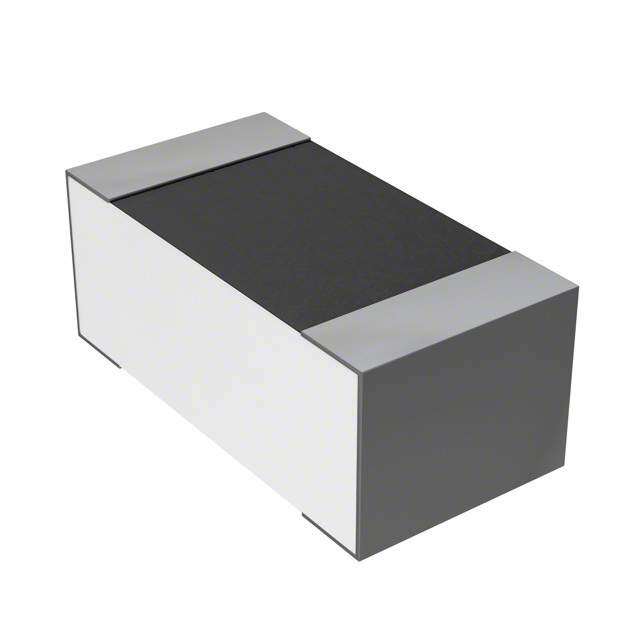
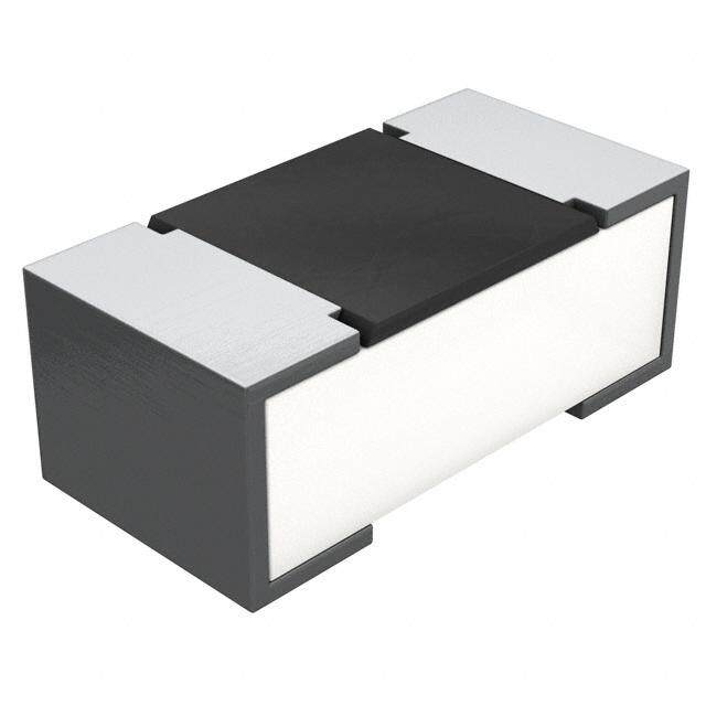
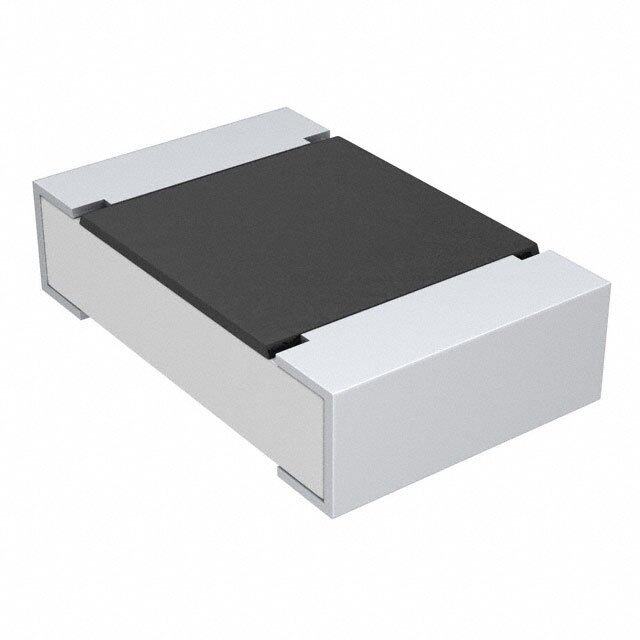
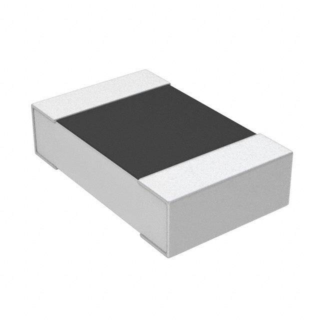
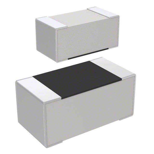
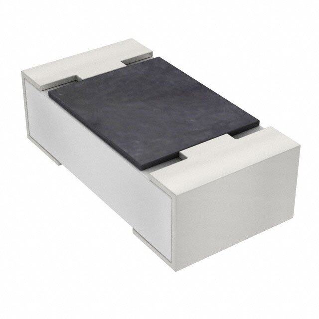
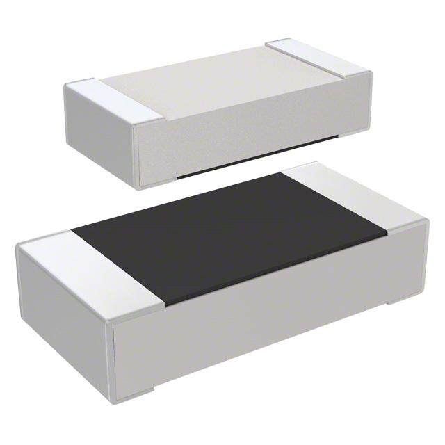
| 描述 | RES 10K OHM 1W 5% 2512 SMD厚膜电阻器 - SMD 2512 10Kohms 5% Tolerance |
| 产品分类 | |
| 品牌 | Panasonic Electronic Components |
| 产品手册 | |
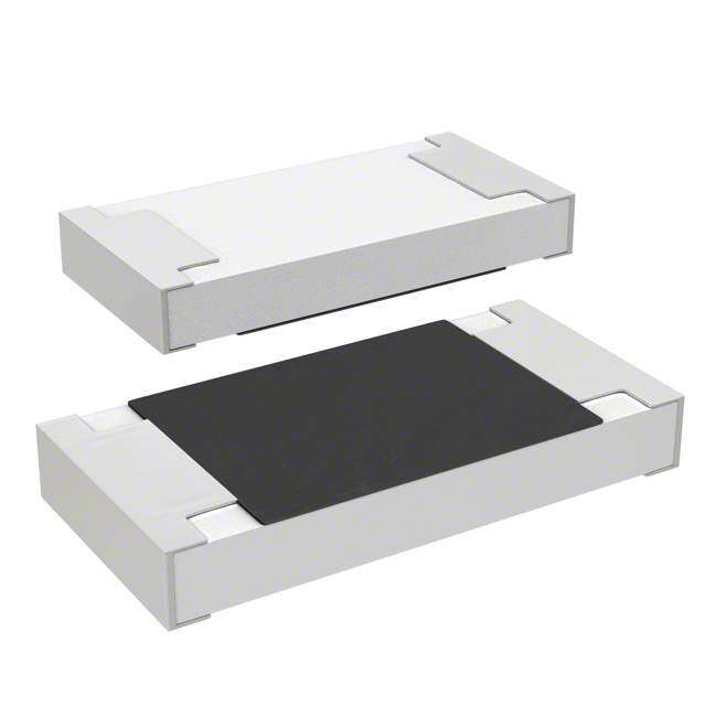
| 产品图片 |
|
| rohs | RoHS 合规性豁免无铅 / 符合限制有害物质指令(RoHS)规范要求 |
| 产品系列 | 薄膜电阻器,厚膜电阻器 - SMD,Panasonic ERJ-1TYJ103UERJ |
| 数据手册 | http://industrial.panasonic.com/www-cgi/jvcr13pz.cgi?E+PZ+3+AOA0001+ERJ1TYJ103U+7+WW |
| 产品型号 | ERJ-1TYJ103U |
| 产品 | Thick Film Resistors SMD |
| 产品目录绘图 |
|
| 产品目录页面 | |
| 产品种类 | 厚膜电阻器 - SMD |
| 供应商器件封装 | 2512 |
| 其它名称 | PT10KXDKR |
| 功率(W) | 1W |
| 功率额定值 | 1 W |
| 包装 | Digi-Reel® |
| 商标 | Panasonic |
| 外壳代码-in | 2512 |
| 外壳代码-mm | 6432 |
| 外壳宽度 | 3.2 mm |
| 外壳长度 | 6.4 mm |
| 外壳高度 | 0.6 mm |
| 大小/尺寸 | 0.252" 长 x 0.126" 宽(6.40mm x 3.20mm) |
| 容差 | ±5% |
| 封装 | Reel |
| 封装/外壳 | 2512(6432 公制) |
| 封装/箱体 | 2512 (6432 metric) |
| 工作温度范围 | - 55 C to + 155 C |
| 工厂包装数量 | 4000 |
| 成分 | 厚膜 |
| 标准包装 | 1 |
| 温度系数 | ±200ppm/°C |
| 特性 | 获得 AEC-Q200 汽车认证 |
| 电压额定值 | 200 V |
| 电阻 | 10 kOhms |
| 电阻(Ω) | 10k |
| 端子数 | 2 |
| 类型 | Thick Film Resistors SMD |
| 系列 | ERJ |
| 高度 | 0.028"(0.70mm) |


- 商务部:美国ITC正式对集成电路等产品启动337调查
- 曝三星4nm工艺存在良率问题 高通将骁龙8 Gen1或转产台积电
- 太阳诱电将投资9.5亿元在常州建新厂生产MLCC 预计2023年完工
- 英特尔发布欧洲新工厂建设计划 深化IDM 2.0 战略
- 台积电先进制程称霸业界 有大客户加持明年业绩稳了
- 达到5530亿美元!SIA预计今年全球半导体销售额将创下新高
- 英特尔拟将自动驾驶子公司Mobileye上市 估值或超500亿美元
- 三星加码芯片和SET,合并消费电子和移动部门,撤换高东真等 CEO
- 三星电子宣布重大人事变动 还合并消费电子和移动部门
- 海关总署:前11个月进口集成电路产品价值2.52万亿元 增长14.8%
PDF Datasheet 数据手册内容提取
2020 Fixed Resistors Products Catalogg 2020.7
(cid:42)(cid:88)(cid:76)(cid:71)(cid:72)(cid:79)(cid:76)(cid:81)(cid:72)(cid:86)(cid:3)(cid:68)(cid:81)(cid:71)(cid:3)(cid:83)(cid:85)(cid:72)(cid:70)(cid:68)(cid:88)(cid:87)(cid:76)(cid:82)(cid:81)(cid:86)(cid:3)(cid:85)(cid:72)(cid:74)(cid:68)(cid:85)(cid:71)(cid:76)(cid:81)(cid:74)(cid:3)(cid:87)(cid:75)(cid:72) (cid:87)(cid:72)(cid:70)(cid:75)(cid:81)(cid:76)(cid:70)(cid:68)(cid:79)(cid:3)(cid:76)(cid:81)(cid:73)(cid:82)(cid:85)(cid:80)(cid:68)(cid:87)(cid:76)(cid:82)(cid:81)(cid:3)(cid:68)(cid:81)(cid:71)(cid:3)(cid:88)(cid:86)(cid:72)(cid:3)(cid:82)(cid:73)(cid:3)(cid:82)(cid:88)(cid:85)(cid:3)(cid:83)(cid:85)(cid:82)(cid:71)(cid:88)(cid:70)(cid:87)(cid:86) (cid:71)(cid:72)(cid:86)(cid:70)(cid:85)(cid:76)(cid:69)(cid:72)(cid:71)(cid:3)(cid:76)(cid:81)(cid:3)(cid:87)(cid:75)(cid:76)(cid:86)(cid:3)(cid:82)(cid:81)(cid:79)(cid:76)(cid:81)(cid:72)(cid:3)(cid:70)(cid:68)(cid:87)(cid:68)(cid:79)(cid:82)(cid:74)(cid:17) (cid:1657)(cid:3)(cid:44)(cid:73)(cid:3)(cid:92)(cid:82)(cid:88)(cid:3)(cid:90)(cid:68)(cid:81)(cid:87)(cid:3)(cid:87)(cid:82)(cid:3)(cid:88)(cid:86)(cid:72)(cid:3)(cid:82)(cid:88)(cid:85)(cid:3)(cid:83)(cid:85)(cid:82)(cid:71)(cid:88)(cid:70)(cid:87)(cid:86)(cid:3)(cid:71)(cid:72)(cid:86)(cid:70)(cid:85)(cid:76)(cid:69)(cid:72)(cid:71)(cid:3)(cid:76)(cid:81)(cid:3)(cid:87)(cid:75)(cid:76)(cid:86)(cid:3)(cid:82)(cid:81)(cid:79)(cid:76)(cid:81)(cid:72)(cid:3)(cid:70)(cid:68)(cid:87)(cid:68)(cid:79)(cid:82)(cid:74)(cid:3)(cid:73)(cid:82)(cid:85)(cid:3)(cid:68)(cid:83)(cid:83)(cid:79)(cid:76)(cid:70)(cid:68)(cid:87)(cid:76)(cid:82)(cid:81)(cid:86)(cid:3)(cid:85)(cid:72)(cid:84)(cid:88)(cid:76)(cid:85)(cid:76)(cid:81)(cid:74)(cid:3) (cid:3)(cid:86)(cid:83)(cid:72)(cid:70)(cid:76)(cid:68)(cid:79)(cid:3)(cid:84)(cid:88)(cid:68)(cid:79)(cid:76)(cid:87)(cid:76)(cid:72)(cid:86)(cid:3)(cid:82)(cid:85)(cid:3)(cid:85)(cid:72)(cid:79)(cid:76)(cid:68)(cid:69)(cid:76)(cid:79)(cid:76)(cid:87)(cid:92)(cid:15)(cid:3)(cid:82)(cid:85)(cid:3)(cid:73)(cid:82)(cid:85)(cid:3)(cid:68)(cid:83)(cid:83)(cid:79)(cid:76)(cid:70)(cid:68)(cid:87)(cid:76)(cid:82)(cid:81)(cid:86)(cid:3)(cid:90)(cid:75)(cid:72)(cid:85)(cid:72)(cid:3)(cid:87)(cid:75)(cid:72)(cid:3)(cid:73)(cid:68)(cid:76)(cid:79)(cid:88)(cid:85)(cid:72)(cid:3)(cid:82)(cid:85)(cid:3)(cid:80)(cid:68)(cid:79)(cid:73)(cid:88)(cid:81)(cid:70)(cid:87)(cid:76)(cid:82)(cid:81)(cid:3)(cid:82)(cid:73)(cid:3)(cid:87)(cid:75)(cid:72)(cid:3) (cid:3)(cid:83)(cid:85)(cid:82)(cid:71)(cid:88)(cid:70)(cid:87)(cid:86)(cid:3)(cid:80)(cid:68)(cid:92)(cid:3)(cid:71)(cid:76)(cid:85)(cid:72)(cid:70)(cid:87)(cid:79)(cid:92)(cid:3)(cid:77)(cid:72)(cid:82)(cid:83)(cid:68)(cid:85)(cid:71)(cid:76)(cid:93)(cid:72)(cid:3)(cid:75)(cid:88)(cid:80)(cid:68)(cid:81)(cid:3)(cid:79)(cid:76)(cid:73)(cid:72)(cid:3)(cid:82)(cid:85)(cid:3)(cid:83)(cid:82)(cid:87)(cid:72)(cid:81)(cid:87)(cid:76)(cid:68)(cid:79)(cid:79)(cid:92)(cid:3)(cid:70)(cid:68)(cid:88)(cid:86)(cid:72)(cid:3)(cid:83)(cid:72)(cid:85)(cid:86)(cid:82)(cid:81)(cid:68)(cid:79)(cid:3)(cid:76)(cid:81)(cid:77)(cid:88)(cid:85)(cid:92)(cid:3) (cid:3)(cid:11)(cid:72)(cid:17)(cid:74)(cid:17)(cid:3)(cid:68)(cid:76)(cid:85)(cid:70)(cid:85)(cid:68)(cid:73)(cid:87)(cid:3)(cid:68)(cid:81)(cid:71)(cid:3)(cid:68)(cid:72)(cid:85)(cid:82)(cid:86)(cid:83)(cid:68)(cid:70)(cid:72)(cid:3)(cid:72)(cid:84)(cid:88)(cid:76)(cid:83)(cid:80)(cid:72)(cid:81)(cid:87)(cid:15)(cid:3)(cid:87)(cid:85)(cid:68)(cid:73)(cid:73)(cid:76)(cid:70)(cid:3)(cid:68)(cid:81)(cid:71)(cid:3)(cid:87)(cid:85)(cid:68)(cid:81)(cid:86)(cid:83)(cid:82)(cid:85)(cid:87)(cid:68)(cid:87)(cid:76)(cid:82)(cid:81)(cid:3)(cid:72)(cid:84)(cid:88)(cid:76)(cid:83)(cid:80)(cid:72)(cid:81)(cid:87)(cid:15)(cid:3)(cid:70)(cid:82)(cid:80)(cid:69)(cid:88)(cid:86)(cid:87)(cid:76)(cid:82)(cid:81)(cid:3) (cid:3)(cid:72)(cid:84)(cid:88)(cid:76)(cid:83)(cid:80)(cid:72)(cid:81)(cid:87)(cid:15)(cid:3)(cid:80)(cid:72)(cid:71)(cid:76)(cid:70)(cid:68)(cid:79)(cid:3)(cid:72)(cid:84)(cid:88)(cid:76)(cid:83)(cid:80)(cid:72)(cid:81)(cid:87)(cid:15)(cid:3)(cid:68)(cid:70)(cid:70)(cid:76)(cid:71)(cid:72)(cid:81)(cid:87)(cid:3)(cid:83)(cid:85)(cid:72)(cid:89)(cid:72)(cid:81)(cid:87)(cid:76)(cid:82)(cid:81)(cid:15)(cid:3)(cid:68)(cid:81)(cid:87)(cid:76)(cid:16)(cid:70)(cid:85)(cid:76)(cid:80)(cid:72)(cid:3)(cid:72)(cid:84)(cid:88)(cid:76)(cid:83)(cid:80)(cid:72)(cid:81)(cid:87)(cid:15)(cid:3)(cid:68)(cid:81)(cid:71)(cid:18)(cid:82)(cid:85)(cid:3)(cid:86)(cid:68)(cid:73)(cid:72)(cid:87)(cid:92)(cid:3) (cid:3)(cid:72)(cid:84)(cid:88)(cid:76)(cid:83)(cid:80)(cid:72)(cid:81)(cid:87)(cid:12)(cid:15)(cid:3)(cid:76)(cid:87)(cid:3)(cid:76)(cid:86)(cid:3)(cid:81)(cid:72)(cid:70)(cid:72)(cid:86)(cid:86)(cid:68)(cid:85)(cid:92)(cid:3)(cid:87)(cid:82)(cid:3)(cid:89)(cid:72)(cid:85)(cid:76)(cid:73)(cid:92)(cid:3)(cid:90)(cid:75)(cid:72)(cid:87)(cid:75)(cid:72)(cid:85)(cid:3)(cid:87)(cid:75)(cid:72)(cid:3)(cid:86)(cid:83)(cid:72)(cid:70)(cid:76)(cid:73)(cid:76)(cid:70)(cid:68)(cid:87)(cid:76)(cid:82)(cid:81)(cid:86)(cid:3)(cid:82)(cid:73)(cid:3)(cid:82)(cid:88)(cid:85)(cid:3)(cid:83)(cid:85)(cid:82)(cid:71)(cid:88)(cid:70)(cid:87)(cid:86)(cid:3)(cid:73)(cid:76)(cid:87)(cid:3)(cid:87)(cid:82)(cid:3)(cid:86)(cid:88)(cid:70)(cid:75)(cid:3) (cid:3)(cid:68)(cid:83)(cid:83)(cid:79)(cid:76)(cid:70)(cid:68)(cid:87)(cid:76)(cid:82)(cid:81)(cid:86)(cid:17)(cid:3)(cid:51)(cid:79)(cid:72)(cid:68)(cid:86)(cid:72)(cid:3)(cid:72)(cid:81)(cid:86)(cid:88)(cid:85)(cid:72)(cid:3)(cid:87)(cid:75)(cid:68)(cid:87)(cid:3)(cid:92)(cid:82)(cid:88)(cid:3)(cid:90)(cid:76)(cid:79)(cid:79)(cid:3)(cid:68)(cid:86)(cid:78)(cid:3)(cid:68)(cid:81)(cid:71)(cid:3)(cid:70)(cid:75)(cid:72)(cid:70)(cid:78)(cid:3)(cid:90)(cid:76)(cid:87)(cid:75)(cid:3)(cid:82)(cid:88)(cid:85)(cid:3)(cid:76)(cid:81)(cid:84)(cid:88)(cid:76)(cid:85)(cid:92)(cid:3)(cid:71)(cid:72)(cid:86)(cid:78)(cid:3)(cid:68)(cid:86)(cid:3)(cid:87)(cid:82)(cid:3)(cid:90)(cid:75)(cid:72)(cid:87)(cid:75)(cid:72)(cid:85) (cid:3)(cid:87)(cid:75)(cid:72)(cid:3)(cid:86)(cid:83)(cid:72)(cid:70)(cid:76)(cid:73)(cid:76)(cid:70)(cid:68)(cid:87)(cid:76)(cid:82)(cid:81)(cid:86)(cid:3)(cid:82)(cid:73)(cid:3)(cid:82)(cid:88)(cid:85)(cid:3)(cid:83)(cid:85)(cid:82)(cid:71)(cid:88)(cid:70)(cid:87)(cid:86)(cid:3)(cid:73)(cid:76)(cid:87)(cid:3)(cid:87)(cid:82)(cid:3)(cid:86)(cid:88)(cid:70)(cid:75)(cid:3)(cid:68)(cid:83)(cid:83)(cid:79)(cid:76)(cid:70)(cid:68)(cid:87)(cid:76)(cid:82)(cid:81)(cid:86)(cid:3)(cid:88)(cid:86)(cid:72)(cid:3)(cid:69)(cid:72)(cid:73)(cid:82)(cid:85)(cid:72)(cid:3)(cid:92)(cid:82)(cid:88)(cid:3)(cid:88)(cid:86)(cid:72)(cid:3)(cid:82)(cid:88)(cid:85)(cid:3)(cid:83)(cid:85)(cid:82)(cid:71)(cid:88)(cid:70)(cid:87)(cid:86)(cid:17) (cid:1657)(cid:3)(cid:55)(cid:75)(cid:72)(cid:3)(cid:84)(cid:88)(cid:68)(cid:79)(cid:76)(cid:87)(cid:92)(cid:3)(cid:68)(cid:81)(cid:71)(cid:3)(cid:83)(cid:72)(cid:85)(cid:73)(cid:82)(cid:85)(cid:80)(cid:68)(cid:81)(cid:70)(cid:72)(cid:3)(cid:82)(cid:73)(cid:3)(cid:82)(cid:88)(cid:85)(cid:3)(cid:83)(cid:85)(cid:82)(cid:71)(cid:88)(cid:70)(cid:87)(cid:86)(cid:3)(cid:68)(cid:86)(cid:3)(cid:71)(cid:72)(cid:86)(cid:70)(cid:85)(cid:76)(cid:69)(cid:72)(cid:71)(cid:3)(cid:76)(cid:81)(cid:3)(cid:87)(cid:75)(cid:76)(cid:86)(cid:3)(cid:82)(cid:81)(cid:79)(cid:76)(cid:81)(cid:72)(cid:3)(cid:70)(cid:68)(cid:87)(cid:68)(cid:79)(cid:82)(cid:74)(cid:3)(cid:82)(cid:81)(cid:79)(cid:92)(cid:3)(cid:68)(cid:83)(cid:83)(cid:79)(cid:92)(cid:3) (cid:3)(cid:87)(cid:82)(cid:3)(cid:82)(cid:88)(cid:85)(cid:3)(cid:83)(cid:85)(cid:82)(cid:71)(cid:88)(cid:70)(cid:87)(cid:86)(cid:3)(cid:90)(cid:75)(cid:72)(cid:81)(cid:3)(cid:88)(cid:86)(cid:72)(cid:71)(cid:3)(cid:76)(cid:81)(cid:3)(cid:76)(cid:86)(cid:82)(cid:79)(cid:68)(cid:87)(cid:76)(cid:82)(cid:81)(cid:17)(cid:3)(cid:55)(cid:75)(cid:72)(cid:85)(cid:72)(cid:73)(cid:82)(cid:85)(cid:72)(cid:15)(cid:3)(cid:83)(cid:79)(cid:72)(cid:68)(cid:86)(cid:72)(cid:3)(cid:72)(cid:81)(cid:86)(cid:88)(cid:85)(cid:72)(cid:3)(cid:92)(cid:82)(cid:88)(cid:3)(cid:72)(cid:89)(cid:68)(cid:79)(cid:88)(cid:68)(cid:87)(cid:72)(cid:3)(cid:68)(cid:81)(cid:71)(cid:3)(cid:89)(cid:72)(cid:85)(cid:76)(cid:73)(cid:92)(cid:3) (cid:3)(cid:82)(cid:88)(cid:85)(cid:3)(cid:83)(cid:85)(cid:82)(cid:71)(cid:88)(cid:70)(cid:87)(cid:86)(cid:3)(cid:88)(cid:81)(cid:71)(cid:72)(cid:85)(cid:3)(cid:87)(cid:75)(cid:72)(cid:3)(cid:86)(cid:83)(cid:72)(cid:70)(cid:76)(cid:73)(cid:76)(cid:70)(cid:3)(cid:70)(cid:76)(cid:85)(cid:70)(cid:88)(cid:80)(cid:86)(cid:87)(cid:68)(cid:81)(cid:70)(cid:72)(cid:86)(cid:3)(cid:76)(cid:81)(cid:3)(cid:90)(cid:75)(cid:76)(cid:70)(cid:75)(cid:3)(cid:82)(cid:88)(cid:85)(cid:3)(cid:83)(cid:85)(cid:82)(cid:71)(cid:88)(cid:70)(cid:87)(cid:86)(cid:3)(cid:68)(cid:85)(cid:72)(cid:3)(cid:68)(cid:86)(cid:86)(cid:72)(cid:80)(cid:69)(cid:79)(cid:72)(cid:71)(cid:3)(cid:76)(cid:81)(cid:3)(cid:92)(cid:82)(cid:88)(cid:85)(cid:3) (cid:3)(cid:82)(cid:90)(cid:81)(cid:3)(cid:83)(cid:85)(cid:82)(cid:71)(cid:88)(cid:70)(cid:87)(cid:86)(cid:3)(cid:68)(cid:81)(cid:71)(cid:3)(cid:76)(cid:81)(cid:3)(cid:90)(cid:75)(cid:76)(cid:70)(cid:75)(cid:3)(cid:82)(cid:88)(cid:85)(cid:3)(cid:83)(cid:85)(cid:82)(cid:71)(cid:88)(cid:70)(cid:87)(cid:86)(cid:3)(cid:90)(cid:76)(cid:79)(cid:79)(cid:3)(cid:68)(cid:70)(cid:87)(cid:88)(cid:68)(cid:79)(cid:79)(cid:92)(cid:3)(cid:69)(cid:72)(cid:3)(cid:88)(cid:86)(cid:72)(cid:71)(cid:17) (cid:1657)(cid:3)(cid:44)(cid:73)(cid:3)(cid:92)(cid:82)(cid:88)(cid:3)(cid:88)(cid:86)(cid:72)(cid:3)(cid:82)(cid:88)(cid:85)(cid:3)(cid:83)(cid:85)(cid:82)(cid:71)(cid:88)(cid:70)(cid:87)(cid:86)(cid:3)(cid:76)(cid:81)(cid:3)(cid:72)(cid:84)(cid:88)(cid:76)(cid:83)(cid:80)(cid:72)(cid:81)(cid:87)(cid:3)(cid:87)(cid:75)(cid:68)(cid:87)(cid:3)(cid:85)(cid:72)(cid:84)(cid:88)(cid:76)(cid:85)(cid:72)(cid:86)(cid:3)(cid:68)(cid:3)(cid:75)(cid:76)(cid:74)(cid:75)(cid:3)(cid:71)(cid:72)(cid:74)(cid:85)(cid:72)(cid:72)(cid:3)(cid:82)(cid:73)(cid:3)(cid:85)(cid:72)(cid:79)(cid:76)(cid:68)(cid:69)(cid:76)(cid:79)(cid:76)(cid:87)(cid:92)(cid:15)(cid:3)(cid:85)(cid:72)(cid:74)(cid:68)(cid:85)(cid:71)(cid:79)(cid:72)(cid:86)(cid:86)(cid:3) (cid:3)(cid:82)(cid:73)(cid:3)(cid:87)(cid:75)(cid:72)(cid:3)(cid:68)(cid:83)(cid:83)(cid:79)(cid:76)(cid:70)(cid:68)(cid:87)(cid:76)(cid:82)(cid:81)(cid:15)(cid:3)(cid:76)(cid:87)(cid:3)(cid:76)(cid:86)(cid:3)(cid:85)(cid:72)(cid:70)(cid:82)(cid:80)(cid:80)(cid:72)(cid:81)(cid:71)(cid:72)(cid:71)(cid:3)(cid:87)(cid:75)(cid:68)(cid:87)(cid:3)(cid:92)(cid:82)(cid:88)(cid:3)(cid:86)(cid:72)(cid:87)(cid:3)(cid:88)(cid:83)(cid:3)(cid:83)(cid:85)(cid:82)(cid:87)(cid:72)(cid:70)(cid:87)(cid:76)(cid:82)(cid:81)(cid:3)(cid:70)(cid:76)(cid:85)(cid:70)(cid:88)(cid:76)(cid:87)(cid:86)(cid:3)(cid:68)(cid:81)(cid:71)(cid:3)(cid:85)(cid:72)(cid:71)(cid:88)(cid:81)(cid:71)(cid:68)(cid:81)(cid:70)(cid:92)(cid:3) (cid:3)(cid:70)(cid:76)(cid:85)(cid:70)(cid:88)(cid:76)(cid:87)(cid:86)(cid:3)(cid:76)(cid:81)(cid:3)(cid:82)(cid:85)(cid:71)(cid:72)(cid:85)(cid:3)(cid:87)(cid:82)(cid:3)(cid:72)(cid:81)(cid:86)(cid:88)(cid:85)(cid:72)(cid:3)(cid:86)(cid:68)(cid:73)(cid:72)(cid:87)(cid:92)(cid:3)(cid:82)(cid:73)(cid:3)(cid:92)(cid:82)(cid:88)(cid:85)(cid:3)(cid:72)(cid:84)(cid:88)(cid:76)(cid:83)(cid:80)(cid:72)(cid:81)(cid:87)(cid:17) (cid:1657)(cid:3)(cid:55)(cid:75)(cid:72)(cid:3)(cid:83)(cid:85)(cid:82)(cid:71)(cid:88)(cid:70)(cid:87)(cid:86)(cid:3)(cid:68)(cid:81)(cid:71)(cid:3)(cid:83)(cid:85)(cid:82)(cid:71)(cid:88)(cid:70)(cid:87)(cid:3)(cid:86)(cid:83)(cid:72)(cid:70)(cid:76)(cid:73)(cid:76)(cid:70)(cid:68)(cid:87)(cid:76)(cid:82)(cid:81)(cid:86)(cid:3)(cid:71)(cid:72)(cid:86)(cid:70)(cid:85)(cid:76)(cid:69)(cid:72)(cid:71)(cid:3)(cid:76)(cid:81)(cid:3)(cid:87)(cid:75)(cid:76)(cid:86)(cid:3)(cid:82)(cid:81)(cid:79)(cid:76)(cid:81)(cid:72)(cid:3)(cid:70)(cid:68)(cid:87)(cid:68)(cid:79)(cid:82)(cid:74)(cid:3)(cid:68)(cid:85)(cid:72)(cid:3)(cid:86)(cid:88)(cid:69)(cid:77)(cid:72)(cid:70)(cid:87)(cid:3)(cid:87)(cid:82)(cid:3) (cid:3)(cid:70)(cid:75)(cid:68)(cid:81)(cid:74)(cid:72)(cid:3)(cid:73)(cid:82)(cid:85)(cid:3)(cid:76)(cid:80)(cid:83)(cid:85)(cid:82)(cid:89)(cid:72)(cid:80)(cid:72)(cid:81)(cid:87)(cid:3)(cid:90)(cid:76)(cid:87)(cid:75)(cid:82)(cid:88)(cid:87)(cid:3)(cid:83)(cid:85)(cid:76)(cid:82)(cid:85)(cid:3)(cid:81)(cid:82)(cid:87)(cid:76)(cid:70)(cid:72)(cid:17)(cid:3)(cid:55)(cid:75)(cid:72)(cid:85)(cid:72)(cid:73)(cid:82)(cid:85)(cid:72)(cid:15)(cid:3)(cid:83)(cid:79)(cid:72)(cid:68)(cid:86)(cid:72)(cid:3)(cid:69)(cid:72)(cid:3)(cid:86)(cid:88)(cid:85)(cid:72)(cid:3)(cid:87)(cid:82)(cid:3)(cid:85)(cid:72)(cid:84)(cid:88)(cid:72)(cid:86)(cid:87)(cid:3)(cid:68)(cid:81)(cid:71)(cid:3) (cid:3)(cid:70)(cid:82)(cid:81)(cid:73)(cid:76)(cid:85)(cid:80)(cid:3)(cid:87)(cid:75)(cid:72)(cid:3)(cid:79)(cid:68)(cid:87)(cid:72)(cid:86)(cid:87)(cid:3)(cid:83)(cid:85)(cid:82)(cid:71)(cid:88)(cid:70)(cid:87)(cid:3)(cid:86)(cid:83)(cid:72)(cid:70)(cid:76)(cid:73)(cid:76)(cid:70)(cid:68)(cid:87)(cid:76)(cid:82)(cid:81)(cid:86)(cid:3)(cid:90)(cid:75)(cid:76)(cid:70)(cid:75)(cid:3)(cid:72)(cid:91)(cid:83)(cid:79)(cid:68)(cid:76)(cid:81)(cid:3)(cid:87)(cid:75)(cid:72)(cid:3)(cid:86)(cid:83)(cid:72)(cid:70)(cid:76)(cid:73)(cid:76)(cid:70)(cid:68)(cid:87)(cid:76)(cid:82)(cid:81)(cid:86)(cid:3)(cid:82)(cid:73)(cid:3)(cid:82)(cid:88)(cid:85)(cid:3)(cid:83)(cid:85)(cid:82)(cid:71)(cid:88)(cid:70)(cid:87)(cid:86)(cid:3)(cid:76)(cid:81)(cid:3) (cid:3)(cid:71)(cid:72)(cid:87)(cid:68)(cid:76)(cid:79)(cid:15)(cid:3)(cid:69)(cid:72)(cid:73)(cid:82)(cid:85)(cid:72)(cid:3)(cid:92)(cid:82)(cid:88)(cid:3)(cid:73)(cid:76)(cid:81)(cid:68)(cid:79)(cid:76)(cid:93)(cid:72)(cid:3)(cid:87)(cid:75)(cid:72)(cid:3)(cid:71)(cid:72)(cid:86)(cid:76)(cid:74)(cid:81)(cid:3)(cid:82)(cid:73)(cid:3)(cid:92)(cid:82)(cid:88)(cid:85)(cid:3)(cid:68)(cid:83)(cid:83)(cid:79)(cid:76)(cid:70)(cid:68)(cid:87)(cid:76)(cid:82)(cid:81)(cid:86)(cid:15)(cid:3)(cid:83)(cid:88)(cid:85)(cid:70)(cid:75)(cid:68)(cid:86)(cid:72)(cid:15)(cid:3)(cid:82)(cid:85)(cid:3)(cid:88)(cid:86)(cid:72)(cid:3)(cid:82)(cid:88)(cid:85)(cid:3)(cid:83)(cid:85)(cid:82)(cid:71)(cid:88)(cid:70)(cid:87)(cid:86)(cid:17) (cid:1657)(cid:3)(cid:55)(cid:75)(cid:72)(cid:3)(cid:87)(cid:72)(cid:70)(cid:75)(cid:81)(cid:76)(cid:70)(cid:68)(cid:79)(cid:3)(cid:76)(cid:81)(cid:73)(cid:82)(cid:85)(cid:80)(cid:68)(cid:87)(cid:76)(cid:82)(cid:81)(cid:3)(cid:76)(cid:81)(cid:3)(cid:87)(cid:75)(cid:76)(cid:86)(cid:3)(cid:82)(cid:81)(cid:79)(cid:76)(cid:81)(cid:72)(cid:3)(cid:70)(cid:68)(cid:87)(cid:68)(cid:79)(cid:82)(cid:74)(cid:3)(cid:83)(cid:85)(cid:82)(cid:89)(cid:76)(cid:71)(cid:72)(cid:86)(cid:3)(cid:72)(cid:91)(cid:68)(cid:80)(cid:83)(cid:79)(cid:72)(cid:86)(cid:3)(cid:82)(cid:73)(cid:3)(cid:82)(cid:88)(cid:85)(cid:3)(cid:83)(cid:85)(cid:82)(cid:71)(cid:88)(cid:70)(cid:87)(cid:86)(cid:10)(cid:3) (cid:3)(cid:87)(cid:92)(cid:83)(cid:76)(cid:70)(cid:68)(cid:79)(cid:3)(cid:82)(cid:83)(cid:72)(cid:85)(cid:68)(cid:87)(cid:76)(cid:82)(cid:81)(cid:86)(cid:3)(cid:68)(cid:81)(cid:71)(cid:3)(cid:68)(cid:83)(cid:83)(cid:79)(cid:76)(cid:70)(cid:68)(cid:87)(cid:76)(cid:82)(cid:81)(cid:3)(cid:70)(cid:76)(cid:85)(cid:70)(cid:88)(cid:76)(cid:87)(cid:86)(cid:17)(cid:3)(cid:58)(cid:72)(cid:3)(cid:71)(cid:82)(cid:3)(cid:81)(cid:82)(cid:87)(cid:3)(cid:74)(cid:88)(cid:68)(cid:85)(cid:68)(cid:81)(cid:87)(cid:72)(cid:72)(cid:3)(cid:87)(cid:75)(cid:72)(cid:3)(cid:81)(cid:82)(cid:81)(cid:16)(cid:76)(cid:81)(cid:73)(cid:85)(cid:76)(cid:81)(cid:74)(cid:72)(cid:80)(cid:72)(cid:81)(cid:87)(cid:3)(cid:82)(cid:73)(cid:3) (cid:3)(cid:87)(cid:75)(cid:76)(cid:85)(cid:71)(cid:3)(cid:83)(cid:68)(cid:85)(cid:87)(cid:92)(cid:10)(cid:86)(cid:3)(cid:76)(cid:81)(cid:87)(cid:72)(cid:79)(cid:79)(cid:72)(cid:70)(cid:87)(cid:88)(cid:68)(cid:79)(cid:3)(cid:83)(cid:85)(cid:82)(cid:83)(cid:72)(cid:85)(cid:87)(cid:92)(cid:3)(cid:85)(cid:76)(cid:74)(cid:75)(cid:87)(cid:86)(cid:3)(cid:68)(cid:81)(cid:71)(cid:3)(cid:90)(cid:72)(cid:3)(cid:71)(cid:82)(cid:3)(cid:81)(cid:82)(cid:87)(cid:3)(cid:74)(cid:85)(cid:68)(cid:81)(cid:87)(cid:3)(cid:68)(cid:81)(cid:92)(cid:3)(cid:79)(cid:76)(cid:70)(cid:72)(cid:81)(cid:86)(cid:72)(cid:15)(cid:3)(cid:85)(cid:76)(cid:74)(cid:75)(cid:87)(cid:15)(cid:3)(cid:82)(cid:85)(cid:3)(cid:76)(cid:81)(cid:87)(cid:72)(cid:85)(cid:72)(cid:86)(cid:87)(cid:3) (cid:76)(cid:81)(cid:3)(cid:82)(cid:88)(cid:85)(cid:3)(cid:76)(cid:81)(cid:87)(cid:72)(cid:79)(cid:79)(cid:72)(cid:70)(cid:87)(cid:88)(cid:68)(cid:79)(cid:3)(cid:83)(cid:85)(cid:82)(cid:83)(cid:72)(cid:85)(cid:87)(cid:92)(cid:17) (cid:1657)(cid:3)(cid:44)(cid:73)(cid:3)(cid:68)(cid:81)(cid:92)(cid:3)(cid:82)(cid:73)(cid:3)(cid:82)(cid:88)(cid:85)(cid:3)(cid:83)(cid:85)(cid:82)(cid:71)(cid:88)(cid:70)(cid:87)(cid:86)(cid:15)(cid:3)(cid:83)(cid:85)(cid:82)(cid:71)(cid:88)(cid:70)(cid:87)(cid:3)(cid:86)(cid:83)(cid:72)(cid:70)(cid:76)(cid:73)(cid:76)(cid:70)(cid:68)(cid:87)(cid:76)(cid:82)(cid:81)(cid:86)(cid:3)(cid:68)(cid:81)(cid:71)(cid:18)(cid:82)(cid:85)(cid:3)(cid:87)(cid:72)(cid:70)(cid:75)(cid:81)(cid:76)(cid:70)(cid:68)(cid:79)(cid:3)(cid:76)(cid:81)(cid:73)(cid:82)(cid:85)(cid:80)(cid:68)(cid:87)(cid:76)(cid:82)(cid:81)(cid:3)(cid:76)(cid:81)(cid:3)(cid:87)(cid:75)(cid:76)(cid:86)(cid:3)(cid:82)(cid:81)(cid:79)(cid:76)(cid:81)(cid:72)(cid:3) (cid:3)(cid:70)(cid:68)(cid:87)(cid:68)(cid:79)(cid:82)(cid:74)(cid:3)(cid:76)(cid:86)(cid:3)(cid:87)(cid:82)(cid:3)(cid:69)(cid:72)(cid:3)(cid:72)(cid:91)(cid:83)(cid:82)(cid:85)(cid:87)(cid:72)(cid:71)(cid:3)(cid:82)(cid:85)(cid:3)(cid:83)(cid:85)(cid:82)(cid:89)(cid:76)(cid:71)(cid:72)(cid:71)(cid:3)(cid:87)(cid:82)(cid:3)(cid:81)(cid:82)(cid:81)(cid:16)(cid:85)(cid:72)(cid:86)(cid:76)(cid:71)(cid:72)(cid:81)(cid:87)(cid:86)(cid:15)(cid:3)(cid:87)(cid:75)(cid:72)(cid:3)(cid:79)(cid:68)(cid:90)(cid:86)(cid:3)(cid:68)(cid:81)(cid:71)(cid:3)(cid:85)(cid:72)(cid:74)(cid:88)(cid:79)(cid:68)(cid:87)(cid:76)(cid:82)(cid:81)(cid:86)(cid:3)(cid:82)(cid:73)(cid:3)(cid:87)(cid:75)(cid:72)(cid:3) (cid:3)(cid:72)(cid:91)(cid:83)(cid:82)(cid:85)(cid:87)(cid:76)(cid:81)(cid:74)(cid:3)(cid:70)(cid:82)(cid:88)(cid:81)(cid:87)(cid:85)(cid:92)(cid:15)(cid:3)(cid:72)(cid:86)(cid:83)(cid:72)(cid:70)(cid:76)(cid:68)(cid:79)(cid:79)(cid:92)(cid:3)(cid:90)(cid:76)(cid:87)(cid:75)(cid:3)(cid:85)(cid:72)(cid:74)(cid:68)(cid:85)(cid:71)(cid:3)(cid:87)(cid:82)(cid:3)(cid:86)(cid:72)(cid:70)(cid:88)(cid:85)(cid:76)(cid:87)(cid:92)(cid:3)(cid:68)(cid:81)(cid:71)(cid:3)(cid:72)(cid:91)(cid:83)(cid:82)(cid:85)(cid:87)(cid:3)(cid:70)(cid:82)(cid:81)(cid:87)(cid:85)(cid:82)(cid:79)(cid:15)(cid:3)(cid:86)(cid:75)(cid:68)(cid:79)(cid:79)(cid:3)(cid:69)(cid:72)(cid:3)(cid:82)(cid:69)(cid:86)(cid:72)(cid:85)(cid:89)(cid:72)(cid:71)(cid:17)(cid:3) (cid:31)(cid:53)(cid:72)(cid:74)(cid:68)(cid:85)(cid:71)(cid:76)(cid:81)(cid:74)(cid:3)(cid:87)(cid:75)(cid:72)(cid:3)(cid:38)(cid:72)(cid:85)(cid:87)(cid:76)(cid:73)(cid:76)(cid:70)(cid:68)(cid:87)(cid:72)(cid:3)(cid:82)(cid:73)(cid:3)(cid:38)(cid:82)(cid:80)(cid:83)(cid:79)(cid:76)(cid:68)(cid:81)(cid:70)(cid:72)(cid:3)(cid:90)(cid:76)(cid:87)(cid:75)(cid:3) (cid:87)(cid:75)(cid:72)(cid:3)(cid:40)(cid:56)(cid:3)(cid:53)(cid:82)(cid:43)(cid:54)(cid:3)(cid:39)(cid:76)(cid:85)(cid:72)(cid:70)(cid:87)(cid:76)(cid:89)(cid:72)(cid:18)(cid:53)(cid:40)(cid:36)(cid:38)(cid:43)(cid:3)(cid:53)(cid:72)(cid:74)(cid:88)(cid:79)(cid:68)(cid:87)(cid:76)(cid:82)(cid:81)(cid:86)(cid:33) (cid:1657)(cid:3)(cid:55)(cid:75)(cid:72)(cid:3)(cid:86)(cid:90)(cid:76)(cid:87)(cid:70)(cid:75)(cid:82)(cid:89)(cid:72)(cid:85)(cid:3)(cid:71)(cid:68)(cid:87)(cid:72)(cid:3)(cid:73)(cid:82)(cid:85)(cid:3)(cid:70)(cid:82)(cid:80)(cid:83)(cid:79)(cid:76)(cid:68)(cid:81)(cid:70)(cid:72)(cid:3)(cid:90)(cid:76)(cid:87)(cid:75)(cid:3)(cid:87)(cid:75)(cid:72)(cid:3)(cid:53)(cid:82)(cid:43)(cid:54)(cid:3)(cid:39)(cid:76)(cid:85)(cid:72)(cid:70)(cid:87)(cid:76)(cid:89)(cid:72)(cid:18)(cid:53)(cid:40)(cid:36)(cid:38)(cid:43)(cid:3)(cid:53)(cid:72)(cid:74)(cid:88)(cid:79)(cid:68)(cid:87)(cid:76)(cid:82)(cid:81)(cid:86)(cid:3)(cid:89)(cid:68)(cid:85)(cid:76)(cid:72)(cid:86)(cid:3) (cid:3)(cid:71)(cid:72)(cid:83)(cid:72)(cid:81)(cid:71)(cid:76)(cid:81)(cid:74)(cid:3)(cid:82)(cid:81)(cid:3)(cid:87)(cid:75)(cid:72)(cid:3)(cid:83)(cid:68)(cid:85)(cid:87)(cid:3)(cid:81)(cid:88)(cid:80)(cid:69)(cid:72)(cid:85)(cid:3)(cid:82)(cid:85)(cid:3)(cid:86)(cid:72)(cid:85)(cid:76)(cid:72)(cid:86)(cid:3)(cid:82)(cid:73)(cid:3)(cid:82)(cid:88)(cid:85)(cid:3)(cid:83)(cid:85)(cid:82)(cid:71)(cid:88)(cid:70)(cid:87)(cid:86)(cid:17) (cid:1657)(cid:3)(cid:58)(cid:75)(cid:72)(cid:81)(cid:3)(cid:92)(cid:82)(cid:88)(cid:3)(cid:88)(cid:86)(cid:72)(cid:3)(cid:87)(cid:75)(cid:72)(cid:3)(cid:76)(cid:81)(cid:89)(cid:72)(cid:81)(cid:87)(cid:82)(cid:85)(cid:92)(cid:3)(cid:82)(cid:73)(cid:3)(cid:82)(cid:88)(cid:85)(cid:3)(cid:83)(cid:85)(cid:82)(cid:71)(cid:88)(cid:70)(cid:87)(cid:86)(cid:3)(cid:73)(cid:82)(cid:85)(cid:3)(cid:90)(cid:75)(cid:76)(cid:70)(cid:75)(cid:3)(cid:76)(cid:87)(cid:3)(cid:76)(cid:86)(cid:3)(cid:88)(cid:81)(cid:70)(cid:79)(cid:72)(cid:68)(cid:85)(cid:3)(cid:90)(cid:75)(cid:72)(cid:87)(cid:75)(cid:72)(cid:85)(cid:3)(cid:87)(cid:75)(cid:82)(cid:86)(cid:72)(cid:3)(cid:83)(cid:85)(cid:82)(cid:71)(cid:88)(cid:70)(cid:87)(cid:86)(cid:3) (cid:3)(cid:68)(cid:85)(cid:72)(cid:3)(cid:70)(cid:82)(cid:80)(cid:83)(cid:79)(cid:76)(cid:68)(cid:81)(cid:87)(cid:3)(cid:90)(cid:76)(cid:87)(cid:75)(cid:3)(cid:87)(cid:75)(cid:72)(cid:3)(cid:53)(cid:82)(cid:43)(cid:54)(cid:3)(cid:39)(cid:76)(cid:85)(cid:72)(cid:70)(cid:87)(cid:76)(cid:89)(cid:72)(cid:18)(cid:53)(cid:40)(cid:36)(cid:38)(cid:43)(cid:3)(cid:53)(cid:72)(cid:74)(cid:88)(cid:79)(cid:68)(cid:87)(cid:76)(cid:82)(cid:81)(cid:15)(cid:3)(cid:83)(cid:79)(cid:72)(cid:68)(cid:86)(cid:72)(cid:3)(cid:86)(cid:72)(cid:79)(cid:72)(cid:70)(cid:87)(cid:3)(cid:5)(cid:54)(cid:68)(cid:79)(cid:72)(cid:86)(cid:3)(cid:44)(cid:81)(cid:84)(cid:88)(cid:76)(cid:85)(cid:92)(cid:5)(cid:3)(cid:76)(cid:81)(cid:3)(cid:87)(cid:75)(cid:72)(cid:3) (cid:3)(cid:90)(cid:72)(cid:69)(cid:86)(cid:76)(cid:87)(cid:72)(cid:3)(cid:76)(cid:81)(cid:84)(cid:88)(cid:76)(cid:85)(cid:92)(cid:3)(cid:73)(cid:82)(cid:85)(cid:80)(cid:3)(cid:68)(cid:81)(cid:71)(cid:3)(cid:70)(cid:82)(cid:81)(cid:87)(cid:68)(cid:70)(cid:87)(cid:3)(cid:88)(cid:86)(cid:17) (cid:58)(cid:72)(cid:3)(cid:71)(cid:82)(cid:3)(cid:81)(cid:82)(cid:87)(cid:3)(cid:87)(cid:68)(cid:78)(cid:72)(cid:3)(cid:68)(cid:81)(cid:92)(cid:3)(cid:85)(cid:72)(cid:86)(cid:83)(cid:82)(cid:81)(cid:86)(cid:76)(cid:69)(cid:76)(cid:79)(cid:76)(cid:87)(cid:92)(cid:3)(cid:73)(cid:82)(cid:85)(cid:3)(cid:87)(cid:75)(cid:72)(cid:3)(cid:88)(cid:86)(cid:72)(cid:3)(cid:82)(cid:73)(cid:3)(cid:82)(cid:88)(cid:85)(cid:3)(cid:83)(cid:85)(cid:82)(cid:71)(cid:88)(cid:70)(cid:87)(cid:86)(cid:3)(cid:82)(cid:88)(cid:87)(cid:86)(cid:76)(cid:71)(cid:72)(cid:3)(cid:87)(cid:75)(cid:72)(cid:3)(cid:86)(cid:70)(cid:82)(cid:83)(cid:72)(cid:3)(cid:82)(cid:73)(cid:3)(cid:87)(cid:75)(cid:72)(cid:3) (cid:86)(cid:83)(cid:72)(cid:70)(cid:76)(cid:73)(cid:76)(cid:70)(cid:68)(cid:87)(cid:76)(cid:82)(cid:81)(cid:86)(cid:15)(cid:3)(cid:71)(cid:72)(cid:86)(cid:70)(cid:85)(cid:76)(cid:83)(cid:87)(cid:76)(cid:82)(cid:81)(cid:86)(cid:15)(cid:3)(cid:74)(cid:88)(cid:76)(cid:71)(cid:72)(cid:79)(cid:76)(cid:81)(cid:72)(cid:86)(cid:3)(cid:68)(cid:81)(cid:71)(cid:3)(cid:83)(cid:85)(cid:72)(cid:70)(cid:68)(cid:88)(cid:87)(cid:76)(cid:82)(cid:81)(cid:86)(cid:3)(cid:71)(cid:72)(cid:86)(cid:70)(cid:85)(cid:76)(cid:69)(cid:72)(cid:71)(cid:3)(cid:76)(cid:81)(cid:3)(cid:87)(cid:75)(cid:76)(cid:86)(cid:3)(cid:82)(cid:81)(cid:79)(cid:76)(cid:81)(cid:72)(cid:3)(cid:70)(cid:68)(cid:87)(cid:68)(cid:79)(cid:82)(cid:74)(cid:17) (cid:19)(cid:20)(cid:16)(cid:36)(cid:83)(cid:85)(cid:16)(cid:20)(cid:28)
Fixed Resistors (Surface Mount Resistors) CONTENTS Classification Product Item Part No. Page Safety Precautions (Common precautions for Fixed Resistors / Common precautions for Surface Mount Resistors) 1 Thick Film Chip Resistors ERJ XG, 1G, 2G, 3G, 6G, 8G, 14, 12, 12Z, 1T 4 General Purpose Chip Resistors Precision Thick Film Chip Resistors ERJ XG, 1G, 1R, 2R, 3R, 6R, 3E, 6E, 8E, 7 ERJ 14, 12, 1T Thin Film Chip Resistors, High Stability and Reliability Type ERA 2V, 3V, 3K, 6V, 6K 11 High Metal Film (Thin Film) Chip Resistors, High Reliability Type ERA 1A, 2A, 3A, 6A, 8A 14 Precision High Precision Thick Film Chip Resistors ERJ PB3, PB6 17 ERJ 2LW, 3LW, 6LW, ERJ 2BW,3BW,6BW,8BW,6CW,8CW Thick Film Chip Resistors / Low Resistance Type ERJ 2B, 3B, 6D, 6B, 8B, 14B, 3R, 6R, 8R, 14R, 19 ERJ 12R, 12Z, ERJ 1TR, L03, L06, L08, L14, L12, L1D, L1W Current Sensing Current Sensing Resistors, Metal Plate Type ERJ MS4S, MS4H, MB1S 25 High Power Chip Resistors / Wide Terminal Type ERJ A1, B1, B2, B3 29 Low TCR High Power Chip Resistors / Wide Terminal Type ERJ D1, D2 33 Small&High Anti-Surge Thick Film Chip Resistors ERJ PA2, P03, PA3, P06, P08, P14 36 Power Anti-Pulse Thick Film Chip Resistors ERJ T06, T08, T14 40 ERJ S02, S03, S06, S08, S14, S12, S1D, S1T, ERJ U0X, U01, U02, U03, U06, U08, U14, U12, Anti-Sulfurated Thick Film Chip Resistors 43 ERJ U1D, ERJ U1T, ERJ U6S, U6Q Anti-Sulfurated Anti-Sulfurated Thick Film Chip Resistors / Precision Type ERJ U2R, U3R, U6R 47 Anti-Sulfurated Thick Film Chip Resistors / Anti-Surge Type ERJ UP3, UP6, UP8 49 Anti-Sulfurated Thick Film Chip Resistors / Wide Terminal Type ERJ C1 52 EXB 14V, 18V, 24V, 28V, N8V, 2HV, 34V, Chip Resistor Array 55 V4V, 38V, V8V, S8V Resistor Anti-Sulfurated Chip Resistor Array EXB U14, U18, U24, U28, U2H, U34, U38 59 Network/Array Chip Resistor Networks EXB D, E, A, Q 62 Chip Attenuator EXB 14AT, 24AT 66 Packaging Methods (Taping) 68 Common Recommended Land Pattern 73 specifications Recommended Soldering Conditions 76 Standard for Resistance Value and Resistance Tolerance 77
Fixed Resistors Safety Precautions (Common precautions for Fixed Resistors) • When using our products, no matter what sort of equipment they might be used for, be sure to make a written agreement on the specifications with us in advance. The design and specifications in this catalog are subject to change without prior notice. • Do not use the products beyond the specifications described in this catalog. • This catalog explains the quality and performance of the products as individual components. Before use, check and evaluate their operations when installed in your products under the actual conditions for use. • Install the following systems for a failsafe design to ensure safety if these products are to be used in equipment where a defect in these products may cause the loss of human life or other significant damage, such as damage to vehicles (automobile, train, vessel), traffic lights, medical equipment, aerospace equipment, electric heating appliances, combustion/gas equipment, rotating equipment, and disaster/crime prevention equipment. ✽ Systems equipped with a protection circuit and a protection device. ✽ Systems equipped with a redundant circuit or other system to prevent an unsafe status in the event of a single fault. ✽ Systems equipped with an arresting the spread of fire or preventing glitch. (1) Precautions for use • These products are designed and manufactured for general and standard use in general elec tron ic equipment. (e.g. AV equipment, home electric appliances, office equipment, information and communication equipment) For applications in which special quality and reliability are required, or if the failure or malfunction of the products may directly jeopardize life or cause threat of personal injury (such as for aircraft and aerospace equipment, traffic and transport equipment, combustion equipment, medical equipment, accident prevention and anti-theft devices, and safety equipment), please be sure to consult with our sales representative in advance and to exchange product specifications which conform to such applications. • These products are not intended for use in the following special conditions. Before using the products, carefully check the effects on their quality and performance, and determine whether or not they can be used. 1. In liquid, such as water, oil, chemicals, or organic solvent. 2. In direct sunlight, outdoors, or in dust. 3. In salty air or air with a high concentration of corrosive gas, such as Cl ,H S,NH ,SO ,or NO . 2 2 3 2 X 4. Electric Static Discharge (ESD) Environment. These components are sensitive to static electricity and can be damaged under static shock (ESD). Please take measures to avoid any of these environments. Smaller components are more sensitive to ESD environment. 5. Electromagnetic and Radioactive Environment. Avoid any environment where strong electromagnetic waves and radiation exist. 6. In an environment where these products cause dew condensation. 7. Sealing or coating of these products or a printed circuit board on which these products are mounted, with resin or other materials. • These products generate Joule heat when energized. Carefully position these products so that their heat will not affect the other components. • Carefully position these products so that their temperatures will not exceed the category temperature range due to the effects of neighboring heat-generating components. Do not mount or place heat-generating components or inflammables, such as vinyl-coated wires, near these products. • Note that non-cleaning solder, halogen-based highly active flux, or water-soluble flux may deteriorate the performance or reliability of the products. • Carefully select a flux cleaning agent for use after soldering. An unsuitable agent may deteriorate the performance or reliability. In particular, when using water or a water-soluble cleaning agent, be careful not to leave water residues. Otherwise, the insulation performance may be deteriorated. • Do not apply flux to these products after soldering. The activity of flux may be a cause of failures in these products. • Refer to the recommended soldering conditions and set the soldering condition. High peak temperature or long heating time may impair the performance or the reliability of these products. • Recommended soldering condition is for the guideline for ensuring the basic characteristics of the products, not for the stable soldering conditions. Conditions for proper soldering should be set up according to individual conditions. 01-Oct-19
Fixed Resistors • Do not reuse any products after removal from mounting boards. • Do not drop these products. If these products are dropped, do not use them. Such products may have received mechanical or electrical damage. • If any doubt or concern to the safety on these products arise, make sure to inform us immediately and conduct technical examinations at your side. (2) Precautions for storage The performance of these products, including the solderability, is guaranteed for a year from the date of arrival at your company, provided that they remain packed as they were when delivered and stored at a temperature of 5 °C to 35 °C and a relative humidity of 45 % to 85 %. Even within the above guarantee periods, do not store these products in the following conditions. Otherwise, their electrical performance and/or solderability may be deteriorated, and the packaging materials (e.g. taping materials) may be deformed or deteriorated, resulting in mounting failures. 1. In salty air or in air with a high concentration of corrosive gas, such as Cl ,H S,NH ,SO ,or NO . 2 2 3 2 X 2. In direct sunlight. (3) AEC-Q200 Compliant The products are tested based on all or part of the test conditions and methods defined in AEC-Q200. Please consult with Panasonic for the details of the product specification and specific evaluation test results, etc., and please review and approve Panasonic's product specification before ordering. <Package markings> Package markings include the product number, quantity, and country of origin. In principle, the country of origin should be indicated in English. 01-Oct-19
Surface Mount Resistors Safety Precautions (Common precautions for Surface Mount Resistors) The following are precautions for individual products. Please also refer to the common precautions for Fixed Resistors in this catalog. 1. Take measures against mechanical stress during and after mounting of Surface Mount Resistors (hereafter called the resistors) so as not to damage their electrodes and protective coatings. Be careful not to misplace the resistors on the land patterns. Otherwise, solder bridging may occur. 2. Keep the rated power and ambient temperature within the specified derating curve. Some circuit boards, wiring patterns, temperatures of heat generated by adjacent components, or ambient temper a tures can become factors in the rise of the temperature of the resistors, regardless of the level of power applied. Therefore, check the conditions before use and op timize them so as not to damage the boards and peripheral components. Make sure to contact us before using the resistors under special conditions. 3. If a transient load (heavy load in a short time) like a pulse is expected to be applied, check and evaluate the operations of the resistors when installed in your products before use. Never exceed the rated power. Otherwise, the performance and/or reliability of the resistors may be impaired. 4. Transient voltage If there is a possibility that the transient phenomenon (significantly high voltage applied in a short time) may occur or that a high voltage pulse may be applied, make sure to evaluate and check the characteristics of resistors mounted on your product rather than only depending on the calculated power limit or steady-state conditions. 5. If the resistors are to be used in high frequency circuits, carefully check the operation before use. Such circuits change the electrical characteristics of the resistors. 6. Before using halogen-based or other high-activity flux, check the possible effects of the flux residues on the performance and reliability of the resistors. 7. When soldering with a soldering iron, never touch the resistors'bodies with the tip of the soldering iron. When using a soldering iron with a high temperature tip, finish soldering as quickly as possible (within three seconds at 350 °C max.). 8. Mounting of the resistors with excessive or insufficient wetting amount of solder may affect the connection reliability or the performance of the resistors. Carefully check the effects and apply a proper amount of solder for use. 9. When the resistors' protective coatings are chipped, flawed, or removed, the characteristics of the resistors may be impaired. Take special care not to apply mechanical shock during automatic mounting or cause damage during handling of the boards with the resistors mounted. 10. Do not apply shock to the resistors or pinch them with a hard tool (e.g. pliers and tweezers). Otherwise, the resistors' protective coatings and bodies may be chipped, affecting their performance. 11. Avoid excessive bending of printed circuit boards in order to protect the resistors from abnormal stress. 12. Do not immerse the resistors in solvent for a long time. Before using solvent, carefully check the effects of immersion. 13. Do not apply excessive tension to the terminals. 01-Oct-19
Thick Film Chip Resistors Thick Film Chip Resistors Series: ERJ XG, 1G, 2G, 3G, 6G, 8G, 14, 12, 12Z, 1T Features ● Small size and lightweight ● High reliability…Metal glaze thick film resistive element and three layers of electrodes ● Compatible with placement machines … Taping packaging available ● Suitable for both reflow and flow soldering ● Reference Standard … IEC 60115-8,JIS C 5201-8,JEITA RC-2134C ● AEC-Q200 compliant (except ERJXG) ● RoHS compliant ■ As for Packaging Methods, Land Pattern, Soldering Conditions and Safety Precautions, Please see Data Files Explanation of Part Numbers 1T ERJS02 ~ ERJS1Tシリーズ ● Series ERJXGN, 1GN, 2GE, 3GE, 6GE, 8GE, 14, 12, 12Z, 1T,±5 % 1 2 3 4 5 6 7 8 9 10 11 12 E R J 3 G E Y J 1 0 2 V Product Code Size, Power Rating Marking Resistance Tolerance Resistance Value Packaging Methods Thick Film Code inch Power Rating Code Marking Code Tolerance The first two digits Code Packaging Part No. Chip Resistors XGN 01005 0.031 W Y MaVrkailnuge on J ±5 % afirgeu rseigsn oiffi craensitstance Y Pressed Carrier Taping 1GN 0201 0.05 W black side 0 Jumper and the third one W8P2, 20,000 pcs ERJXGN 2GE 0402 0.1 W *Nil No marking denotes number of Embossed Carrier Taping zeros following. U 3GE 0603 0.1 W W4P1, 40,000 pcs Jumper is expressed 6GE 0805 0.125 W by R00. Pressed Carrier Taping C ERJ1GN 8GE 1206 0.25 W (Ex.) 222: 2.2 kΩ 2 mm pitch, 15,000 pcs 4R7: 4.7 Ω 14 1210 0.5 W Punched Carrier Taping X ERJ2GE 12 1812 0.75 W 2 mm pitch, 10,000 pcs 12Z 2010 0.75 W ERJ3GE Punched Carrier Taping 1T 2512 1 W V 4 mm pitch, 5,000 pcs ERJ6GE ERJ8GE *Series XGN, 1GN and 2GE do not have value markings on the black side. ERJ14 Embossed Carrier Taping Please omit the letter "Y" from the part number for these series of parts. ERJ12 U The other part number factors will move up respectively. 4 mm pitch, 5,000 pcs ERJ12Z Embossed Carrier Taping ERJ1T 4 mm pitch, 4,000 pcs Design and specifications are each subject to change without notice. Ask factory for the current technical specifications before purchase and/or use. Should a safety concern arise regarding this product, please be sure to contact us immediately. 26-Jun-20
Thick Film Chip Resistors Ratings 【For Resistor】 Limiting Maximum Category Power Rating Resistance Resistance AEC- Part No. Element Overload T.C.R. Temperature (inch size) at 70 °C(1) Voltage(2) Voltage(3) Tolerance Range (×10-6/K) Range Q200 (W) (%) (Ω) Grade (V) (V) (℃) R<10 Ω : –100 to +600 ERJXG 0.031 15 30 ±5 1 to 1 M (E24) 10 Ω to 100 Ω : ±300 -55 to +125 - (01005) 100 Ω≤R : ±200 ERJ1G 0.05 25 50 ±5 1 to 10 M (E24) -55 to +125 Grade 1 (0201) ERJ2G 0.1 50 100 ±5 1 to 10 M (E24) -55 to +155 Grade 0 (0402) R<10 Ω : ERJ3G –100 to +600 0.1 75 150 ±5 1 to 10 M (E24) -55 to +155 Grade 0 (0603) ERJ6G 0.125 150 200 ±5 1 to 10 M (E24) -55 to +155 Grade 0 (0805) 10 Ω to 1 M Ω : ERJ8G ±200 0.25 200 400 ±5 1 to 10 M (E24) -55 to +155 Grade 0 (1206) ERJ14 0.5 200 400 ±5 1 to 10 M (E24) -55 to +155 Grade 0 (1210) 1 MΩ<R : ERJ12 –400 to +150 0.75 200 500 ±5 1 to 10 M (E24) -55 to +155 Grade 0 (1812) ERJ12Z 0.75 200 500 ±5 1 to 10 M (E24) -55 to +155 Grade 0 (2010) ERJ1T 1 200 500 ±5 1 to 1 M (E24) -55 to +155 Grade 0 (2512) (1) Use it on the condition that the case temperature is below the upper category temperature. (2) Rated Continuous Working Voltage (RCWV) shall be determined from RCWV=√Power Rating × Resistance Value, or Limiting Element Voltage listed above, whichever less. (3) Overload Test Voltage (OTV) shall be determined from OTV=Specified Magnification (refer to performance) × RCWV or Maximum Overload Voltage listed above, whichever less. 【For Jumper】 Power Derating Curve Maximum Overload Part No. Resistance(Ω) Rated Current(A) Current (A)(1) For resistors operated in ambient temperatures ERJXG above 70 °C, power rating shall be derated in 0.5 1 ERJ1G accordance with the figure below. ERJ2G -55 ℃ 70 ℃ 1 2 100 ERJ3G ERJ6G 50 mΩ or less ad 80 ER1J42,G 1,2 3, G1,2 6ZG, ,1 8TG, ERJ8G Lo 60 d ERJ14 e 40 ERJ12 2 4 Rat ERJXG,1G 155 ℃ 20 ERJ12Z 125 ℃ 0 ERJ1T -60 -40 -20 0 20 40 60 80 100 120140 160180 (1) Overload test current Ambient Temperature (°C) Construction Protective coating Electrode (Inner) Aluminasubstrate Electrode (Between) Thick film resistive element Electrode (Outer) Design and specifications are each subject to change without notice. Ask factory for the current technical specifications before purchase and/or use. Should a safety concern arise regarding this product, please be sure to contact us immediately. 26-Jun-20
Thick Film Chip Resistors Dimensions in mm (not to scale) L a W T b Dimensions (mm) Mass (Weight) Part No. L W a b T (g/1000 pcs) ERJXG 0.40±0.02 0.20±0.02 0.10±0.03 0.10±0.03 0.13±0.02 0.04 ERJ1G 0.60±0.03 0.30±0.03 0.10±0.05 0.15±0.05 0.23±0.03 0.15 ERJ2G 1.00±0.05 0.50±0.05 0.20±0.10 0.25±0.05 0.35±0.05 0.8 ERJ3G 1.60±0.15 0.80+0.15/-0.05 0.30±0.20 0.30±0.15 0.45±0.10 2 ERJ6G 2.00±0.20 1.25±0.10 0.40±0.20 0.40±0.20 0.60±0.10 4 ERJ8G 3.20+0.05/-0.20 1.60+0.05/-0.15 0.50±0.20 0.50±0.20 0.60±0.10 10 ERJ14 3.20±0.20 2.50±0.20 0.50±0.20 0.50±0.20 0.60±0.10 16 ERJ12 4.50±0.20 3.20±0.20 0.50±0.20 0.50±0.20 0.60±0.10 27 ERJ12Z 5.00±0.20 2.50±0.20 0.60±0.20 0.60±0.20 0.60±0.10 27 ERJ1T 6.40±0.20 3.20±0.20 0.65±0.20 0.60±0.20 0.60±0.10 45 Performance Performance Requirements ⊿R Test Item Test Conditions Resistor type Jumper type Within Specified Resistance 50 mΩ or less 20 °C Tolerance Within Specified T. C. R. 50 mΩ or less +25 °C/+155 °C (ERJXG,1G : +25 °C/+125 °C) T. C. R. Rated Voltage× 2.5,5 s Overload ±2 % 50 mΩ or less Jumper type : Max. Overload Current, 5 s Resistance to ±1 % 50 mΩ or less 270 °C, 10 s Soldering Heat Rapid Change of –55 °C (30 min.) / +155 °C (ERJXG,1G : +125 °C) ±1 % 50 mΩ or less Temperature (30 min.),100 cycles High Temperature ±1 % 50 mΩ or less +155 °C (ERJXG,1G : +125 °C), 1000 h Exposure Damp Heat, Steady ±1 % 50 mΩ or less 60 °C, 90 % to 95 %RH, 1000 h State 60 °C, 90 % to 95 %RH, Rated Voltage (Jumper type : Load Life in Humidity ±3 % 50 mΩ or less Rated Current), 1.5 h ON / 0.5 h OFF cycle, 1000 h 70 °C,Rated Voltage (Jumper type :Rated Current), Endurance at 70 °C ±3 % 50 mΩ or less 1.5 h ON / 0.5 h OFF cycle, 1000 h Design and specifications are each subject to change without notice. Ask factory for the current technical specifications before purchase and/or use. Should a safety concern arise regarding this product, please be sure to contact us immediately. 26-Jun-20
Precision Thick Film Chip Resistors Precision Thick Film Chip Resistors Series: ERJ XG, 1G ERJ 1R, 2R, 3R, 6R ERJ 3E, 6E, 8E, 14, 12, 1T Features ● Small size and lightweight ● High reliability…Metal glaze thick film resistive element and three layers of electrodes ● Compatible with placement machines … Taping packaging available ● Suitable for both reflow and flow soldering ● Low Resistance Tolerance :E RJXG, 1G, 2R, 3E, 6E, 8E, 14, 12, 1T :±1 % ERJ1R, 2R, 3R, 6R :±0.5 % ● Reference Standard … IEC 60115-8,JIS C 5201-8,JEITA RC-2134C ● AEC-Q200 compliant (except ERJXG,ERJ1R) ● RoHS compliant ■ As for Packaging Methods, Land Pattern, Soldering Conditions and Safety Precautions, Please see Data Files Explanation of Part Numbers 1T ERJS02 ~ ERJS1Tシリーズ ● Series ERJ1R, 2R, 3R, 6R, ±0.5 % 1 2 3 4 5 6 7 8 9 10 11 12 E R J 3 R B D 1 0 0 2 V Product Code Size, Power Rating T.C.R.,Marking Resistance Tolerance Packaging Methods Thick Film Code inch Power Rating Code T.C.R. Code Tolerance Code Packaging Part No. Chip Resistors 1R 0201 0.05 W H ±50 ×10–6/K (1R, 2R) D ±0.5 % Pressed Carrier Taping C ERJ1R 2R 0402 0.063 W B ±50 ×10–6/K (3R, 6R) 2 mm pitch, 15,000 pcs 3R 0603 0.1 W K ±100 ×10–6/K (2R) Resistance Value Punched Carrier Taping X ERJ2R 6R 0805 0.1 W E ±100 ×10–6/K (3R, 6R) The first three digits are 2 mm pitch, 10,000 pcs significant figures of resistance and the last V Punched Carrier Taping ERJ3R one denotes number of 4 mm pitch, 5,000 pcs ERJ6R zeros following. (Ex.) 1002: 10 KΩ Design and specifications are each subject to change without notice. Ask factory for the current technical specifications before purchase and/or use. Should a safety concern arise regarding this product, please be sure to contact us immediately. 1-Mar-20
Precision Thick Film Chip Resistors ● Series ERJXGN, 1GN, 2RC, 2RK, 3EK, 6EN, 8EN, 14N, 12N, 12S, 1TN, ±1 % 1 2 3 4 5 6 7 8 9 10 11 12 E R J 8 E N F 1 0 0 2 V Product Code Size, Power Rating Resistance Tolerance Resistance Value Packaging Methods Thick Film Code inch Power Rating Code Tolerance The first three digits are Code Packaging Part No. Chip Resistors XGN 01005 0.031 W F ±1 % significant figures of resistance Pressed Carrier Taping Y 1GN 0201 0.05 W and the last one denotes W8P2, 20,000 pcs ERJXGN 2RC 0402 0.1 W number of zeros following. Embossed Carrier Taping U 2RK 0402 0.1 W Decimal point is expressed by W4P1, 40,000 pcs 3EK 0603 0.1 W "R". Pressed Carrier Taping C ERJ1GN 6EN 0805 0.125 W (Ex.)1002: 10 kΩ 2 mm pitch, 15,000 pcs 8EN 1206 0.25 W Punched Carrier Taping ERJ2RC X 14N 1210 0.5 W 2 mm pitch, 10,000 pcs ERJ2RK 12N 1812 0.75 W ERJ3EK Punched Carrier Taping 12S 2010 0.75 W V ERJ6EN 4 mm pitch, 5,000 pcs 1TN 2512 1 W ERJ8EN ERJ14N Embossed Carrier Taping ERJ12N U 4 mm pitch, 5,000 pcs ERJ12S Embossed Carrier Taping ERJ1TN 4 mm pitch, 4,000 pcs Ratings <±0.5 %> Limiting Maximum Category Power Rating Resistance Resistance AEC- Part No. Element Overload T.C.R. Temperature (inch size) at 70 °C(1) Voltage(2) Voltage(3) Tolerance Range (×10-6/K) Range Q200 (W) (%) (Ω) Grade (V) (V) (℃) ERJ1RH 0.05 15 30 ±0.5 1 k to 1 M (E24,E96) ±50 -55 to +125 - (0201) ERJ2RH 0.063 50 100 ±0.5 100 to 100 k (E24,E96) ±50 -55 to +155 Grade 0 (0402) ERJ2RK 10 to 97.6 0.063 50 100 ±0.5 (E24,E96) ±100 -55 to +155 Grade 0 (0402) 102 k to 1 M ERJ3RB 0.1 50 100 ±0.5 100 to 100 k (E24,E96) ±50 -55 to +155 Grade 0 (0603) ERJ3RE 10 to 97.6 0.1 50 100 ±0.5 (E24,E96) ±100 -55 to +155 Grade 0 (0603) 102 k to 1 M ERJ6RB 0.1 150 200 ±0.5 100 to 100 k (E24,E96) ±50 -55 to +155 Grade 0 (0805) ERJ6RE 10 to 97.6 0.1 150 200 ±0.5 (E24,E96) ±100 -55 to +155 Grade 0 (0805) 102 k to 1 M (1) Use it on the condition that the case temperature is below the upper category temperature. (2) Rated Continuous Working Voltage (RCWV) shall be determined from RCWV=√Power Rating × Resistance Value, or Limiting Element Voltage listed above, whichever less. (3) Overload Test Voltage (OTV) shall be determined from OTV=Specified Magnification (refer to performance) × RCWV or Maximum Overload Voltage listed above, whichever less. Design and specifications are each subject to change without notice. Ask factory for the current technical specifications before purchase and/or use. Should a safety concern arise regarding this product, please be sure to contact us immediately. 1-Mar-20
Precision Thick Film Chip Resistors Ratings <±1 %> Limiting Maximum Category Power Rating Resistance Resistance AEC- Part No. Element Overload T.C.R. Temperature (inch size) at 70 °C(1) Voltage(2) Voltage(3) Tolerance Range (×10-6/K) Range Q200 (W) (%) (Ω) Grade (V) (V) (℃) ERJXGN R<100 Ω : ±300 0.031 15 30 ±1 10 to 1 M (4) (E24,E96) -55 to +125 - (01005) 100 Ω ≤R : ±200 ERJ1GN 0.05 25 50 ±1 10 to 1 M (4) (E24,E96) ±200 -55 to +125 Grade 1 (0201) ERJ2RC 0.1 50 100 ±1 1 to 9.76 (E24,E96) –100 to +600 -55 to +155 Grade 0 (0402) ERJ2RK 0.1 50 100 ±1 10 to 1 M (E24,E96) ±100 -55 to +155 Grade 0 (0402) ERJ3EK 0.1 75 150 ±1 10 to 1 M (E24,E96) ±100 -55 to +155 Grade 0 (0603) ERJ6EN 0.125 150 200 ±1 10 to 2.2 M (E24,E96) ±100 -55 to +155 Grade 0 (0805) ERJ8EN 0.25 200 400 ±1 10 to 2.2 M (E24,E96) ±100 -55 to +155 Grade 0 (1206) ERJ14N 0.5 200 400 ±1 10 to 1 M (E24,E96) ±100 -55 to +155 Grade 0 (1210) ERJ12N 0.75 200 500 ±1 10 to 1 M (E24,E96) ±100 -55 to +155 Grade 0 (1812) ERJ12S 0.75 200 500 ±1 10 to 1 M (E24,E96) ±100 -55 to +155 Grade 0 (2010) ERJ1TN 1 200 500 ±1 10 to 1 M (E24,E96) ±100 -55 to +155 Grade 0 (2512) (1) Use it on the condition that the case temperature is below the upper category temperature. (2) Rated Continuous Working Voltage (RCWV) shall be determined from RCWV=√Power Rating × Resistance Value, or Limiting Element Voltage listed above, whichever less. (3) Overload Test Voltage (OTV) shall be determined from OTV=Specified Magnification (refer to performance) × RCWV or Maximum Overload Voltage listed above, whichever less. (4) Please contact us when you need a type with a resistance of less than 10 Ω. Power Derating Curve For resistors operated in ambient temperatures -55 ℃ 70 ℃ ) %100 above 70 °C, power rating shall be derated in ( accordance with the figure on the right. ad 80 Lo 60 d e 40 t Ra ERJXG,1G, 1R 155 ℃ 20 125 ℃ 0 -60 -40 -20 0 20 40 60 80 100 120140 160180 Ambient Temperature (°C) Construction Protective coating Electrode (Inner) Aluminasubstrate Electrode (Between) Thick film resistive element Electrode (Outer) Design and specifications are each subject to change without notice. Ask factory for the current technical specifications before purchase and/or use. Should a safety concern arise regarding this product, please be sure to contact us immediately. 1-Mar-20
Precision Thick Film Chip Resistors Dimensions in mm (not to scale) L a W T b Dimensions (mm) Mass (Weight) Part No. L W a b T (g/1000 pcs) ERJXGN 0.40±0.02 0.20±0.02 0.10±0.03 0.10±0.03 0.13±0.02 0.04 ERJ1GN 0.60±0.03 0.30±0.03 0.10±0.05 0.15±0.05 0.23±0.03 0.15 ERJ1R□ ERJ2R□ 1.00±0.05 0.50±0.05 0.20±0.10 0.25±0.05 0.35±0.05 0.8 ERJ3R□ 1.60±0.15 0.80+0.15/-0.05 0.30±0.20 0.30±0.15 0.45±0.10 2 ERJ3EK ERJ6R□ 2.00±0.20 1.25±0.10 0.40±0.20 0.40±0.20 0.60±0.10 4 ERJ6EN ERJ8EN 3.20+0.05/-0.20 1.60+0.05/-0.15 0.50±0.20 0.50±0.20 0.60±0.10 10 ERJ14N 3.20±0.20 2.50±0.20 0.50±0.20 0.50±0.20 0.60±0.10 16 ERJ12N 4.50±0.20 3.20±0.20 0.50±0.20 0.50±0.20 0.60±0.10 27 ERJ12S 5.00±0.20 2.50±0.20 0.60±0.20 0.60±0.20 0.60±0.10 27 ERJ1TN 6.40±0.20 3.20±0.20 0.65±0.20 0.60±0.20 0.60±0.10 45 Performance ● Series ERJ1R, 2R, 3R, 6R, ±0.5 %(D) Performance Test Item Test Conditions Requirements ⊿R Within Specified Resistance 20 °C Tolerance Within Specified T. C. R. +25 °C/+125 °C T. C. R. Overload ±2 % Rated Voltage× 2.5,5 s Resistance to Soldering Heat ±1 % 270 °C, 10 s –55 °C (30 min.) / +155 °C (ERJ1R : +125 °C)(30 min.), Rapid Change of Temperature ±1 % 100 cycles High Temperature Exposure ±1 % +155 °C (ERJ1R : +125 °C), 1000 h Damp Heat, Steady State ±1 % 60 °C, 90 % to 95 %RH, 1000 h ±2 % 60 °C, 90 % to 95 %RH, Rated Voltage, Load Life in Humidity ERJ1R : ±3 % 1.5 h ON / 0.5 h OFF cycle, 1000 h ±2 % Endurance at 70 °C 70 °C,Rated Voltage,1.5 h ON / 0.5 h OFF cycle,1000 h ERJ1R : ±3 % ● Series ERJXGN, 1GN, 2RC, 2RK, 3EK, 6EN, 8EN, 14N, 12N, 12S, 1TN, ±1 %(F) Performance Test Item Test Conditions Requirements ⊿R Within Specified Resistance 20 °C Tolerance Within Specified T. C. R. +25 °C/+155 °C (ERJXG,ERJ1G : +25℃/+125 °C) T. C. R. Overload ±2 % Rated Voltage× 2.5,5 s Resistance to Soldering Heat ±1 % 270 °C, 10 s –55 °C (30 min.)/+155 °C (ERJXG,ERJ1G : +125 °C)(30 min.), Rapid Change of Temperature ±1 % 100 cycles High Temperature Exposure ±1 % +155 °C (ERJXG,ERJ1G : +125 °C), 1000 h Damp Heat, Steady State ±1 % 60 °C, 90 % to 95 %RH, 1000 h ±2 % 60 °C, 90 % to 95 %RH, Rated Voltage, Load Life in Humidity ERJXG,1G : ±3 % 1.5 h ON / 0.5 h OFF cycle, 1000 h ±2 % Endurance at 70 °C 70 °C,Rated Voltage,1.5 h ON / 0.5 h OFF cycle,1000 h ERJXG,1G : ±3 % Design and specifications are each subject to change without notice. Ask factory for the current technical specifications before purchase and/or use. Should a safety concern arise regarding this product, please be sure to contact us immediately. 1-Mar-20
Thin Film Chip Resistors, High Stability and Reliability Type NEW Thin Film Chip Resistors, High Stability and Reliability Type ERA V (High resistance value ERA K) Series: ERA 2V, 3V, 6V (Series: ERA 3K, 6K ) Features ● High reliability……… Stable at high temperature and humidity (85 °C 85 %RH rated load, Category temperature range : –55 °C to +155 °C) ● High accuracy……… Low resistance tolerance and Temperature Coefficient of Resistance ● High performance… Low current noise, excellent linearity ● Anti-ESD………………Original structure for high ESD performance (AEC-Q200-002 HBM Level 1c and above) ● Anti-sulfurated………Original structure for sulfurated performance ● Reference Standard…… IEC 60115-8, JIS C 5201-8, JEITA RC-2133C ● AEC-Q200 compliant ● RoHS compliant ■ As for Packaging Methods, Land Pattern, Soldering Conditions and Safety Precautions, Please see Data Files Explanation of Part Numbers 1T ERJS02 ~ ERJS1Tシリーズ 1 2 3 4 5 6 7 8 9 10 11 12 E R A 3 V E B 1 0 5 1 V Product Code Size, Power Rating Temperature Coefficient Resistance Tolerance Resistance Value Packaging Methods Thin Film Code inch Power Rating Code T.C.R. Code Tolerance Consist of four Code Packaging Part No. figures.The first Chip Resistors 2V 0402 0.063 W R ±10×10-6/K W ±0.05 % three digits are X Punched Carrier Taping ERA2V 3V P ±15×10-6/K B ±0.1 % significant figures of 2 mm pitch, 10,000 pcs 0603 0.1 W 3K E ±25×10-6/K resistance and the ERA3V fourth one denotes Punched Carrier Taping ERA3K 6V V 0805 0.125 W number of zeros 4 mm pitch, 5,000 pcs ERA6V 6K following. ERA6K (Ex.) 1051 : 1.05 kΩ Design and specifications are each subject to change without notice. Ask factory for the current technical specifications before purchase and/or use. Should a safety concern arise regarding this product, please be sure to contact us immediately. 7-Feb-20
Thin Film Chip Resistors, High Stability and Reliability Type Ratings Limiting Maximum Resistance Category Part No. Power Rating Element Overload Part No. Tolerance T.C.R. Resistance Range(4) Temperature AEC-Q200 (inch size) at 85 °C(1) Voltage(2) Voltage(3) (detail) Range Grade (W) (V) (V) (%) (×10-6/K) (Ω) (℃) ERA2VEB ±0.1 ±25 47 to 10 k (E24, E96) ERA2V ERA2VPB ±0.1 ±15 0.063 50 100 (0402) ERA2VRB ±0.1 1 K to 10 k (E24, E96) ±10 ERA2VRW ±0.05 ERA3VEB ±0.1 ±25 47 to 100 k (E24, E96) ERA3V ERA3VPB ±0.1 ±15 0.1 75 150 (0603) ERA3VRB ±0.1 1 K to 100 k (E24, E96) ±10 ERA3VRW ±0.05 –55 to +155 Grade 0 ERA3K 0.1 75 150 ERA3KEB ±0.1 ±25 102 K to 240 k (E24, E96) (0603) ERA6VEB ±0.1 ±25 47 to 100 k (E24, E96) ERA6V ERA6VPB ±0.1 ±15 0.125 100 200 (0805) ERA6VRB ±0.1 1 K to 100 k (E24, E96) ±10 ERA6VRW ±0.05 ERA6K 0.125 100 200 ERA6KEB ±0.1 ±25 102 K to 750 k (E24, E96) (0805) (1) Use it on the condition that the case temperature is below the upper category temperature. (2) Rated Continuous Working Voltage (RCWV) shall be determined from RCWV=√Power Rating × Resistance Values, or Limiting Element Voltage listed above, whichever less. (3) Overload Test Voltage (OTV) shall be determined from OTV=Specified Magnification (2.5) × RCWV or Maximum Overload Voltage listed above, whichever less. (4) E192 series resistance values are also available. The E192 series has custom part numbers. Please contact us for details. Power Derating Curve -55 ℃ 85 ℃ ) 100 For resistors operated in ambient temperatures % above 85 °C, power rating shall be derated in d ( 80 a o accordance with the figure on the right. L 60 d e t 40 a R 20 155 ℃ 0 -60 -40 -20 0 20 40 60 80 100 120 140 160 180 Ambient Temperature (°C) Construction Protective coating Electrode (Inner) Electrode (Between) Alumina substrate Electrode (Outer) High reliability metal film Design and specifications are each subject to change without notice. Ask factory for the current technical specifications before purchase and/or use. Should a safety concern arise regarding this product, please be sure to contact us immediately. 7-Feb-20
Thin Film Chip Resistors, High Stability and Reliability Type Dimensions in mm (not to scale) L a W T b Dimensions (mm) Mass (Weight) Part No. L W a b T (g/1000 pcs) ERA2V 1.00±0.05 0.50+0.10/-0.05 0.25±0.10 0.25±0.10 0.35±0.05 0.6 ERA3V, 3K 1.60±0.15 0.80±0.10 0.30±0.20 0.30±0.20 0.45±0.10 2 ERA6V, 6K 2.00±0.20 1.25±0.10 0.40±0.20 0.40±0.20 0.55±0.10 5 Performance Performance Test Item Test Conditions Requirements ⊿R Within Specified Resistance 20 °C Tolerance Within Specified T. C. R. +25 °C/+125 °C T. C. R. Overload ±0.1 % Rated Voltage× 2.5,5 s Resistance to ±0.1 % 270 °C, 10 s Soldering Heat Rapid Change of ±0.1 % –55 °C (30 min.) / +155 °C (30 min.),1000 cycles Temperature High Temperature ±0.1 % +155 °C, 1000 h Exposure Damp Heat, Steady ±0.1 % 85 °C, 85 %RH, 1000 h State 85 °C, 85 %RH, 10 % of Rated Power(1), Load Life in Humidity ±0.1 % 1.5 h ON / 0.5 h OFF cycle , 1000 h Endurance at 85 °C ±0.1 % 85 °C ,Rated Voltage,1.5 h ON / 0.5 h OFF cycle,1000 h AEC-Q200-002 : 150 pF, 2000 Ω , positive 5 times, negative 5 times Electro Static ERA2V : 1.0 kV (level 1c) ±0.1 %(2) Discharge (HBM) ERA3V(3K) : 1.5 kV (level 1c) ERA6V(6K) : 2.0 kV (level 2) (1) Applied Voltage is "√0.1 × Power Rating × Resistance Values ", or "Limiting Element Voltage×0.316", whichever less. (2) Depends on resistance value. Design and specifications are each subject to change without notice. Ask factory for the current technical specifications before purchase and/or use. Should a safety concern arise regarding this product, please be sure to contact us immediately. 7-Feb-20
Metal Film (Thin Film) Chip Resistors, High Reliability Type Metal Film (Thin Film) Chip Resistors, High Reliability Type Series: ERA 1A, 2A, 3A, 6A, 8A Features ● High reliability………S table at high temperature and humidity (85 °C 85 %RH rated load, Category temperature range : –55 °C to +155 °C) ● High accuracy……… Low resistance tolerance and Temperature Coefficient of Resistance ● High performance… Low current noise, excellent linearity ● Reference Standard…… IEC 60115-8, JIS C 5201-8, JEITA RC-2133C ● AEC-Q200 compliant (except ERA1A) ● RoHS compliant ■ As for Packaging Methods, Land Pattern, Soldering Conditions and Safety Precautions, Please see Data Files Explanation of Part Numbers 1T ERJS02 ~ ERJS1Tシリーズ ● E24 Series 1 2 3 4 5 6 7 8 9 10 11 E R A 3 A E B 1 0 2 V Product Code Size, Power Rating Temp. Coefficient Resistance Tolerance Resistance Value Packaging Methods Thin Film Code inch size Power Rating Code T.C.R. Code Tolerance Consist of three figures Code Packaging Part No. Chip Resistors 1A 0201 0.05 W R ±10×10-6/K W ±0.05 % froers iEst2a4n csee rvieaslue. C Pressed Carrier Taping ERA1A 2A 0402 0.063 W P ±15×10-6/K B ±0.1 % The first two digits are 2 mm pitch, 15,000 pcs 3A 0603 0.1 W E ±25×10-6/K C ±0.25 % significant figures of Punched Carrier Taping resistance and the third X ERA2A 6A 0805 0.125 W H ±50×10-6/K D ±0.5 % 2 mm pitch, 10,000 pcs one denotes number of 8A 1206 0.25 W K ±100×10-6/K zeros following. Punched Carrier Taping ERA3A (example) 102 : 1 kΩ V 4 mm pitch, 5,000 pcs ERA6A ERA8A ● E96 Series and other Resistance values 1 2 3 4 5 6 7 8 9 10 11 12 E R A 3 A E B 1 0 5 1 V Product Code Size, Power Rating Temp. Coefficient Resistance Tolerance Resistance Value Packaging Methods Thin Film Code inch size Power Rating Code T.C.R. Code Tolerance Consist of four figures Code Packaging Part No. Chip Resistors 1A 0201 0.05 W R ±10×10-6/K W ±0.05 % froers iEst9a6n csee rvieaslue. C Pressed Carrier Taping ERA1A 2A 0402 0.063 W P ±15×10-6/K B ±0.1 % The first three digits 2 mm pitch, 15,000 pcs 3A 0603 0.1 W E ±25×10-6/K C ±0.25 % are significant figures Punched Carrier Taping of resistance and the X ERA2A 6A 0805 0.125 W H ±50×10-6/K D ±0.5 % 2 mm pitch, 10,000 pcs fourth one denotes 8A 1206 0.25 W K ±100×10-6/K number of zeros Punched Carrier Taping ERA3A following. V 4 mm pitch, 5,000 pcs ERA6A (example) ERA8A 1051 : 1.05 kΩ Note : Duplicated resistance values as E24 series part umbers shall follow E24 part numbers. (apply three digit resistance value) Design and specifications are each subject to change without notice. Ask factory for the current technical specifications before purchase and/or use. Should a safety concern arise regarding this product, please be sure to contact us immediately. 8-Jun-20
Metal Film (Thin Film) Chip Resistors, High Reliability Type Ratings Limiting Maximum Category (iPnacrht sNizoe.) Poawt 8er5 R°aCt(i1n)g VEoleltmageen(t2) VOovletarlgoea(d3) (Pdaertta Nil)o. RTeosleisrtaannccee T.C.R. RReasnigstea(4n)c(5e) TemRpaenrgaeture AEGCr-aQd2e00 (W) (V) (V) (%) (×10-6/K) (Ω) (℃) ERA1AEB ±0.1 ±25 100 to 10 k (E24,E96) ERA1AEC ±0.25 ERA1A 0.05 25 50 ERA1ARC ±0.25 - (0201) 100 to 10 k (E24,E96) ERA1ARB ±0.1 ±10 ERA1ARW ±0.05 1 k to 10 k (E24,E96) ERA2AKD ±0.5 ±100 10 to 46.4 (E24,E96) ERA2AED ±0.5 ERA2AEC ±0.25 ±25 47 to 100 k (E24,E96) ERA2A ERA2AEB ±0.1 0.063 50 100 Grade 1 (0402) ERA2APC ±0.25 ±15 200 to 47 k (E24,E96) ERA2APB ±0.1 ERA2ARC ±0.25 ±10 200 to 47 k (E24,E96) ERA2ARB ±0.1 ERA3AHD ±0.5 ±50 10 to 46.4 (E24,E96) ERA3AED ±0.5 ERA3AEC ±0.25 ±25 47 to 330 k (E24,E96) ERA3AEB ±0.1 ERA3A 0.1 75 150 ERA3APC ±0.25 Grade 0 (0603) ±15 470 to 100 k (E24,E96) ERA3APB ±0.1 ERA3ARC ±0.25 –55 to +155 ERA3ARB ±0.1 ±10 1 k to 100 k (E24,E96) ERA3ARW ±0.05 ERA6AHD ±0.5 ±50 10 to 46.4 (E24,E96) ERA6AED ±0.5 ERA6AEC ±0.25 ±25 47 to 1 M (E24,E96) ERA6AEB ±0.1 ERA6A 0.125 100 200 ERA6APC ±0.25 Grade 0 (0805) ±15 470 to 100 k (E24,E96) ERA6APB ±0.1 ERA6ARC ±0.25 ERA6ARB ±0.1 ±10 1 k to 100 k (E24,E96) ERA6ARW ±0.05 ERA8AHD ±0.5 ±50 10 to 46.4 (E24,E96) ERA8AED ±0.5 ERA8AEC ±0.25 ±25 47 to 1 M (E24,E96) ERA8AEB ±0.1 ERA8A 0.25 150 300 ERA8APC ±0.25 Grade 0 (1206) ±15 470 to 100 k (E24,E96) ERA8APB ±0.1 ERA8ARC ±0.25 ERA8ARB ±0.1 ±10 1 k to 100 k (E24,E96) ERA8ARW ±0.05 (1) Use it on the condition that the case temperature is below the upper category temperature. (2) Rated Continuous Working Voltage (RCWV) shall be determined from RCWV=√Power Rating × Resistance Values, or Limiting Element Voltage listed above, whichever less. (3) Overload Test Voltage (OTV) shall be determined from OTV=Specified Magnification (2.5) × RCWV or Maximum Overload Voltage listed above, whichever less. (4) E192 series resistance values are also available. Please contact us for details. (5) Duplicated resistance values between E96, E192 and E24 series shall follow E24 Part Numbers. (apply three digit resistance value) -55 ℃ 85 ℃ Power Derating Curve 100 For resistors operated in ambient temperatures ) % 80 above 85 °C, power rating shall be derated in ( d accordance with the figure on the right. oa 60 L d e 40 t a R 20 155 ℃ 0 -60 -40 -20 0 20 40 60 80 100 120 140 160 180 Ambient Temperature (°C) Design and specifications are each subject to change without notice. Ask factory for the current technical specifications before purchase and/or use. Should a safety concern arise regarding this product, please be sure to contact us immediately. 8-Jun-20
Metal Film (Thin Film) Chip Resistors, High Reliability Type Construction Protective coating Electrode (Inner) Alumina substrate Electrode (Between) High reliability metal film Electrode (Outer) *0402 size, 0603 size and E96 series do not have value markings. Dimensions in mm (not to scale) L a W T b Dimensions (mm) Mass (Weight) Part No. L W a b T (g/1000 pcs) ERA1A 0.60±0.03 0.30±0.03 0.15±0.05 0.15±0.05 0.23±0.03 0.14 ERA2A 1.00±0.10 0.50+0.10/-0.05 0.15±0.10 0.25±0.10 0.35±0.05 0.6 ERA3A 1.60±0.20 0.8±0.20 0.30±0.20 0.30±0.15 0.45±0.10 2 ERA6A 2.00±0.20 1.25±0.10 0.40±0.25 0.40±0.25 0.60±0.10 4 ERA8A 3.20±0.20 1.60+0.05/-0.15 0.50±0.25 0.50±0.25 0.60±0.10 8 Design and specifications are each subject to change without notice. Ask factory for the current technical specifications before purchase and/or use. Should a safety concern arise regarding this product, please be sure to contact us immediately. 8-Jun-20
High Precision Thick Film Chip Resistors High Precision Thick Film Chip Resistors Series: ERJ PB3, PB6 Features ● Achieve the resistance tolerance ±0.1 % with high reliability metal glaze thick film resistor −6 ● Guarantee the temperature coefficient of Resistance ±50×10 /K in high resistance range up to 1 MΩ ● High power … 0.20 W:0603 inch /1608 mm size(ERJPB3) 0.25 W:0805 inch /2012 mm size(ERJPB6) ● Reference Standard … IEC 60115-8,JIS C 5201-8,JEITA RC-2134C ● AEC-Q200 compliant ● RoHS compliant ■ As for Packaging Methods, Land Pattern, Soldering Conditions and Safety Precautions, Please see Data Files Explanation of Part Numbers 1T ERJS02 ~ ERJS1Tシリーズ 1 2 3 4 5 6 7 8 9 10 11 12 E R J P B 6 B 1 0 0 2 V Product Code Size, Power Rating Resistance Tolerance Resistance Value Packaging Methods Thick Film Power Code Tolerance The first three digits are Code Packaging Part No. Code inch Chip Resistors Rating B ±0.1 % significant figures of Punched Carrier Taping ERJPB3 resistance and the last V PB3 0603 0.20 W D ±0.5 % 4 mm pitch, 5,000 pcs ERJPB6 one denotes number of PB6 0805 0.25 W zeros following. (Ex.) 5110 : 511 Ω 1003 : 100 kΩ Ratings Limiting Maximum Category Power Rating Resistance Resistance AEC- Part No. Element Overload T.C.R. Temperature (inch size) at 70 °C(1) Voltage(2) Voltage(3) Tolerance Range (×10-6/K) Range Q200 (W) (%) (Ω) Grade (V) (V) (℃) ERJPB3 ±0.1 200 to 100 k 0.20 150 200 ±50 –55 to +155 Grade 0 (0603) ±0.5 (E24, E96) ERJPB6 ±0.1 200 to 1 M 0.25 150 200 ±50 –55 to +155 Grade 0 (0805) ±0.5 (E24, E96) (1) Use it on the condition that the case temperature is below the upper category temperature. (2) Rated Continuous Working Voltage (RCWV) shall be determined from RCWV=√Power Rating × Resistance Value, or Limiting Element Voltage listed above, whichever less. (3) Overload Test Voltage (OTV) shall be determined from OTV=Specified Magnification (refer to performance) × RCWV or Maximum Overload Voltage listed above, whichever less. Power Derating Curve -55 ℃ 70 ℃ For resistors operated in ambient temperatures 100 ) % above 70 °C, power rating shall be derated in ( 80 accordance with the figure on the right. oad 60 L d 40 e t 155 ℃ Ra 20 0 -60 -40-20 0 20 40 60 80 100 120140160 180 Ambient Temperature (°C) Design and specifications are each subject to change without notice. Ask factory for the current technical specifications before purchase and/or use. Should a safety concern arise regarding this product, please be sure to contact us immediately. 1-Mar-20
High Precision Thick Film Chip Resistors Construction Protective coating Electrode (Inner) Aluminasubstrate Electrode (Between) Thick film resistive element Electrode (Outer) Dimensions in mm (not to scale) L a W T b Dimensions (mm) Mass (Weight) Part No. L W a b T (g/1000 pcs) ERJPB3 1.60±0.15 0.80+0.15/-0.05 0.15+0.15/-0.10 0.25±0.10 0.45±0.10 2 ERJPB6 2.00±0.20 1.25±0.10 0.25±0.20 0.40±0.20 0.60±0.10 4 Performance Performance Test Item Test Conditions Requirements ⊿R Within Specified Resistance 20 °C Tolerance Within Specified T. C. R. +25 °C/+125 °C T. C. R. Overload ±0.5 % Rated Voltage× 2.0,5 s Resistance to Soldering Heat ±0.5 % 270 °C, 10 s Rapid Change of Temperature ±0.5 % –55 °C (30 min.) / +155 °C (30 min.),100 cycles High Temperature Exposure ±0.5 % +155 °C, 1000 h Damp Heat, Steady State ±0.5 % 60 °C, 90 % to 95 %RH, 1000 h 60 °C, 90 % to 95 %RH, Rated Voltage, Load Life in Humidity ±0.5 % 1.5 h ON / 0.5 h OFF cycle, 1000 h Endurance at 70 °C ±0.5 % 70 °C,Rated Voltage , 1.5 h ON / 0.5 h OFF cycle, 1000 h Design and specifications are each subject to change without notice. Ask factory for the current technical specifications before purchase and/or use. Should a safety concern arise regarding this product, please be sure to contact us immediately. 1-Mar-20
Thick Film Chip Resistors / Low Resistance Type Thick Film Chip Resistors / Low Resistance Type Series: ERJ 2LW, 3LW, 6LW, ERJ 2BW, 3BW, 6BW, 8BW, 6CW, 8CW ERJ 2B, 3B, 6D, 6B, 8B, 14B, ERJ 3R, 6R, 8R, 14R, 12R, 12Z, 1TR ERJ L03, L06, L08, L14, L12, L1D, L1W Features ● Current Sensing resistor ● Small size and lightweight ● Realize both low-resistance & High-precision by original thick film resistive element & special electrode structure ● Suitable for both reflow and flow soldering ● Realize High-power by double-sided resistive elements structure that aimed to suppress temperature rising… ERJ2LW, 3LW, 6LW, 2BW, 3BW, 6BW, 8BW, 6CW, 8CW ● Low TCR………………… ±75×10-6/K(ERJ6CW, ERJ8CW) ● Low Resistance Value… Thick film resistors available from 5 mΩ (ERJ3LW, 6LW) ● Reference Standard…… IEC 60115-8, JIS C 5201-8, JEITA RC-2144 ● AEC-Q200 compliant ● RoHS compliant ■ As for Packaging Methods, Land Pattern, Soldering Conditions and Safety Precautions, Please see Data Files Explanation of Part Numbers ● ERJ2LW, 3LW, 6LW, 2BW, 3BW, 6BW, 8BW, 6CW, 8CW <High power (double-sided resistive elements structure) type> 1 2 3 4 5 6 7 8 9 10 11 12 E R J 2 B W G R 0 4 7 X Product Code Code inch size Power Rating Resistance Value Resistance Tolerance Resistance Value Packaging Methods Thick Film 2LW 0402 0.2 W 10 mΩ Code Tolerance Shown by 4 digits or Code Packaging Part No. letters. Chip Resistors 3LW 0603 0.25 W 5 mΩ, 10 mΩ D ±0.5 %* (Ex.) X Pressed Carrier Taping ERJ2LW 6LW 0805 0.5 W 5, 6, 7, 8, 9 mΩ F ±1 % R005 : 0.05 Ω = 5 mΩ 2 mm pitch, 10,000 pcsERJ2BW 2BW 0402 0.25 W 47 m to 100 mΩ G ±2 % R047 : 0.047 Ω = 47 mΩ ERJ3LW 3BW 0603 0.33 W 20 m to 100 mΩ J ±5 % ERJ6LW 6BW 0805 0.5 W 10 m to 100 mΩ *Please refer to the rating table Punched Carrier Taping ERJ3BW V ERJ6BW 8BW 1206 1 W 10 m to 100 mΩ for the resistance tolerance. 4 mm pitch, 5,000 pcs ERJ8BW 6CW 0805 0.5 W 10 m to 30 mΩ ERJ6CW ERJ8CW 8CW 1206 1 W 10 m to 50 mΩ Design and specifications are each subject to change without notice. Ask factory for the current technical specifications before purchase and/or use. Should a safety concern arise regarding this product, please be sure to contact us immediately. 29-Jan-20
Thick Film Chip Resistors / Low Resistance Type ● ERJ2BS/2BQ, 3BS/3BQ, 6BS/6BQ, 8BS/8BQ, 14BS/14BQ, 6D, 3R, 6R, 8R, 14R, 12R, 12Z, 1TR <High power type/Standard type> 1 2 3 4 5 6 7 8 9 10 11 E R J 8 R Q F R 2 2 V Product Code Size, Power Rating Resistance Value Region Resistance Tolerance Resistance Value Packaging Methods Thick Film Code inch size Power Rating S 0.1Ω to 0.2Ω Code Tolerance Shown by 3 Code Packaging Part No. Chip Resistors 2B 0402 0.166 W Q 0.22Ω to 9.1Ω ✽ D ±0.5 %* digits or letters. Punched Carrier Taping X ERJ2B 3B 0603 0.25 W ✽2B:0.22 Ω to 1.0 Ω F ±1 % Only when it is D 2 mm pitch,10,000 pcs 3R 0603 0.1 W G ±2 % (E24,E96) or F ERJ3B/3R 6D 0805 0.5 W J ±5 % (E96), shown by Punched Carrier Taping ERJ6D/6B/ V 6B 0805 0.33 W *Please refer to the 4 digits or 4 mm pitch, 5,000 pcs ERJ6R 6R 0805 0.125 W rating table for the letters. ERJ8B/8R 8B 1206 0.5 W resistance tolerance. (Ex.) ERJ14B/14R 8R 1206 0.25 W R22 : 0.22 Ω Embossed Carrier Taping ERJ12R 14B 1210 0.5 W R102 : 0.102 Ω U 4 mm pitch, 5,000 pcs ERJ12Z 14R 1210 0.25 W Embossed Carrier Taping ERJ1TR 12R 1812 0.5 W 4 mm pitch, 4,000 pcs 12Z 2010 0.5 W 1TR 2512 1 W ● ERJL03, L06, L08, L14, L12, L1D, L1W <Low TCR type> 1 2 3 4 5 6 7 8 9 10 11 12 E R J L 1 4 K J 5 0 M U Product Code Size, Power Rating Code Resistance Value Resistance Tolerance Resistance Value Packaging Methods Thick Film Code inch size Power Rating Standard ✽ Code Tolerance Shown by 3 Code Packaging Part No. Chip Resistors L03 0603 0.2 W 20 mΩ, 22 mΩ, F ±1 % digits or letters. ERJL03 Punched Carrier Taping L06 0805 0.25 W K 33 mΩ, 39 mΩ, J ±5 % (Ex.) V ERJL06 4 mm pitch, 5,000 pcs L08 1206 0.33 W 47 mΩ, 50 mΩ, 50M : 50 mΩ, ERJL08 L14 1210 0.33 W 100mΩ 10C : 100 mΩ ERJL14 Embossed Carrier Taping L12 1812 0.5 W U 20 mΩ to 100 mΩ ✽ ERJL12 4 mm pitch, 5,000 pcs L1D 2010 0.5 W ✽ L03, L06, L08 : 47 mΩ to 100 mΩ U ERJL1D L1W 2512 1 W L1D, L1W : 40 mΩ to 100 mΩ Embossed Carrier Taping ERJL1W 4 mm pitch, 3,000 pcs Ratings <High power (double-sided resistive elements structure) type> Power Rating Resistance Resistance Category AEC- Part No. T.C.R. at 70 °C(1) Tolerance Range(2) Temperature Q200 (inch size) (×10-6/K) (W) (%) (Ω) Range(℃) Grade ERJ2LW (0402) 0.2 ±1, ±2, ±5 10 m 0 to +500 –55 to +125 Grade 1 5 m 0 to +700 –55 to +125 ERJ3LW (0603) 0.25 ±1, ±2, ±5 Grade 1 10 m 0 to +300 –55 to +125 ERJ6LW (0805) 0.5 ±1, ±2, ±5 5, 6, 7, 8, 9 m 0 to +300 –55 to +125 Grade 1 ERJ2BW (0402) 0.25 ±1, ±2, ±5 47 m to 100 m(E24) 0 to +300 –55 to +155 Grade 0 20 mΩ ≤ R < 39 mΩ:0 to +250 ERJ3BW (0603) 0.33 ±1, ±2, ±5 20 m to 100 m(E24) –55 to +155 Grade 0 39 mΩ ≤ R ≤ 100 mΩ:0 to +150 10 mΩ ≤ R < 15 mΩ:0 to +300 ERJ6BW (0805) 0.5 ±1, ±2, ±5 10 m to 100 m(E24) –55 to +155 Grade 0 15 mΩ ≤ R ≤ 100 mΩ:0 to +200 10 mΩ ≤ R < 20 mΩ:0 to +200 ERJ8BW (1206) 1 ±1, ±2, ±5 10 m to 100 m(E24) 20 mΩ ≤ R < 47 mΩ:0 to +150 –55 to +155 Grade 0 47 mΩ ≤ R ≤ 100 mΩ:0 to +100 ERJ6CW (0805) 0.5 ±0.5, ±1, ±2, ±5 10 m to 30 m (E24) ±75 –55 to +125 Grade 1 ERJ8CW (1206) 1 ±1, ±2, ±5 10 m to 50 m (E24) ±75 –55 to +125 Grade 1 (1) Use it on the condition that the case temperature is below the upper category temperature. ・ Rated Continuous Working Voltage (RCWV) shall be determined from RCWV=√Power Rating × Resistance Value. ・ Overload Test Voltage (OTV) shall be determined from OTV=Specified Magnification (refer to performance) × RCW. (2) Please contact us when resistors of irregular series are needed. Design and specifications are each subject to change without notice. Ask factory for the current technical specifications before purchase and/or use. Should a safety concern arise regarding this product, please be sure to contact us immediately. 29-Jan-20
Thick Film Chip Resistors / Low Resistance Type Ratings <High power type> Power Rating Resistance Resistance Category AEC- Part No. T.C.R. at 70 °C(1) Tolerance(2) Range(3) Temperature Q200 (inch size) (×10-6/K) (W) (%) (Ω) Range(℃) Grade ERJ2BS (0402) 0.10 to 0.20 (E24) 0.10 Ω ≤ R < 0.22 Ω : 0 to +300 0.166 ±1, ±2, ±5 –55 to +155 Grade 0 ERJ2BQ (0402) 0.22 to 1.0 (E24) 0.22 Ω ≤ R ≤ 1.0 Ω : 0 to +250 ERJ3BS (0603) 0.10 to 0.20 (E24) 0.10 Ω ≤ R < 0.22 Ω : 0 to +300 0.25 ±1, ±2, ±5 0.22 to 0.91 (E24) 0.22 Ω ≤ R < 1.0 Ω : 0 to +300 –55 to +155 Grade 0 ERJ3BQ (0603) 1.0 to 9.1 (E24) 1.0 Ω ≤ R ≤ 9.1 Ω : ±200 ERJ6DS (0805) 0.10 to 0.20 (E24,E96) 0.10 Ω ≤ R < 0.22 Ω : 0 to +150 0.5 ±0.5, ±1, ±2, ±5 0.22 Ω ≤ R < 1.0 Ω : 0 to +100 –55 to +155 Grade 0 ERJ6DQ (0805) 0.22 to 9.1 (E24,E96) 1.0 Ω ≤ R ≤ 9.1 Ω : ±100 ERJ6BS (0805) 0.10 to 0.20 (E24) 0.10 Ω ≤ R < 0.22 Ω : 0 to +250 0.33 ±1, ±2, ±5 0.22 to 0.91 (E24) 0.22 Ω ≤ R < 1.0 Ω : 0 to +250 –55 to +155 Grade 0 ERJ6BQ (0805) 1.0 to 9.1 (E24) 1.0 Ω ≤ R ≤ 9.1 Ω : ±200 ERJ8BS (1206) 0.10 to 0.20 (E24) 0.10 Ω ≤ R < 0.22 Ω : 0 to +250 0.5 ±1, ±2, ±5 0.22 to 0.91 (E24) 0.22 Ω ≤ R < 1.0 Ω : 0 to +250 –55 to +155 Grade 0 ERJ8BQ (1206) 1.0 to 9.1 (E24) 1.0 Ω ≤ R ≤ 9.1 Ω : ±200 ERJ14BS (1210) 0.10 to 0.20 (E24) 0.10 Ω ≤ R < 0.22 Ω : 0 to +200 0.5 ±1, ±2, ±5 0.22 to 0.91 (E24) 0.22 Ω ≤ R < 1.0 Ω : 0 to +200 –55 to +155 Grade 0 ERJ14BQ (1210) 1.0 to 9.1 (E24) 1.0 Ω ≤ R ≤ 9.1 Ω : ±100 (1) Use it on the condition that the case temperature is below the upper category temperature. (2) E96 series also have ±0.5 %, ±1 % line-up. ・ Rated Continuous Working Voltage (RCWV) shall be determined from RCWV=√Power Rating × Resistance Value. ・ Overload Test Voltage (OTV) shall be determined from OTV=Specified Magnification (refer to performance) × RCW. (3) Please contact us when resistors of irregular series are needed. <Standard type> Power Rating Resistance Resistance Category AEC- Part No. T.C.R. at 70 °C(1) Tolerance Range(2) Temperature Q200 (inch size) (×10-6/K) (W) (%) (Ω) Range(℃) Grade ERJ3RS (0603) 0.10 to 0.20 (E24) 0.10 Ω ≤ R < 0.22 Ω : 0 to +300 0.1 ±1, ±2, ±5 0.22 to 0.91 (E24) 0.22 Ω ≤ R < 1.0 Ω : 0 to +300 –55 to +155 Grade 0 ERJ3RQ (0603) 1.0 to 9.1 (E24) 1.0 Ω ≤ R ≤ 9.1 Ω : ±200 ERJ6RS (0805) 0.10 to 0.20 (E24) 0.10 Ω ≤ R < 0.22 Ω : 0 to +250 0.125 ±1, ±2, ±5 0.22 to 0.91 (E24) 0.22 Ω ≤ R < 1.0 Ω : 0 to +250 –55 to +155 Grade 0 ERJ6RQ (0805) 1.0 to 9.1 (E24) 1.0 Ω ≤ R ≤ 9.1 Ω : ±200 ERJ8RS (1206) 0.10 to 0.20 (E24) 0.10 Ω ≤ R < 0.22 Ω : 0 to +250 0.25 ±1, ±2, ±5 0.22 to 0.91 (E24) 0.22 Ω ≤ R < 1.0 Ω : 0 to +250 –55 to +155 Grade 0 ERJ8RQ (1206) 1.0 to 9.1 (E24) 1.0 Ω ≤ R ≤ 9.1 Ω : ±200 ERJ14RS (1210) 0.10 to 0.20 (E24) 0.10 Ω ≤ R < 0.22 Ω : 0 to +200 0.25 ±1, ±2, ±5 0.22 to 0.91 (E24) 0.22 Ω ≤ R < 1.0 Ω : 0 to +200 –55 to +155 Grade 0 ERJ14RQ (1210) 1.0 to 9.1 (E24) 1.0 Ω ≤ R ≤ 9.1 Ω : ±100 ERJ12RS (1812) 0.10 to 0.20 (E24) 0.10 Ω ≤ R < 0.22 Ω : 0 to +200 0.5 ±1, ±2, ±5 0.22 to 0.91 (E24) 0.22 Ω ≤ R < 1.0 Ω : 0 to +200 –55 to +155 Grade 0 ERJ12RQ (1812) 1.0 to 9.1 (E24) 1.0 Ω ≤ R ≤ 9.1 Ω : ±100 ERJ12ZS (2010) 0.10 to 0.20 (E24) 0.10 Ω ≤ R < 0.22 Ω : 0 to +200 0.5 ±1, ±2, ±5 0.22 to 0.91 (E24) 0.22 Ω ≤ R < 1.0 Ω : 0 to +200 –55 to +155 Grade 0 ERJ12ZQ (2010) 1.0 to 9.1 (E24) 1.0 Ω ≤ R ≤ 9.1 Ω : ±100 ERJ1TRS (2512) 0.10 to 0.20 (E24) 0.10 Ω ≤ R < 0.22 Ω : 0 to +200 1 ±1, ±2, ±5 0.22 to 0.91 (E24) 0.22 Ω ≤ R < 1.0 Ω : 0 to +200 –55 to +155 Grade 0 ERJ1TRQ (2512) 1.0 to 9.1 (E24) 1.0 Ω ≤ R ≤ 9.1 Ω : ±100 (1) Use it on the condition that the case temperature is below the upper category temperature. ・ Rated Continuous Working Voltage (RCWV) shall be determined from RCWV=√Power Rating × Resistance Value. ・ Overload Test Voltage (OTV) shall be determined from OTV=Specified Magnification (refer to performance) × RCW. (2) Please contact us when resistors of irregular series are needed. Design and specifications are each subject to change without notice. Ask factory for the current technical specifications before purchase and/or use. Should a safety concern arise regarding this product, please be sure to contact us immediately. 29-Jan-20
Thick Film Chip Resistors / Low Resistance Type Ratings <Low TCR type> Power Rating Resistance Resistance Category AEC- Part No. T.C.R. at 70 °C(1) Tolerance Range(2) Temperature Q200 (inch size) (×10-6/K) (W) (%) (Ω) Range(℃) Grade ERJL03 (0603) 0.2 ±1, ±5 47 m to 100 m ±200 –55 to +125 Grade 1 ERJL06 (0805) 0.25 ±1, ±5 47 m to 100 m ±100 –55 to +125 Grade 1 ERJL08 (1206) 0.33 ±1, ±5 47 m to 100 m ±100 –55 to +125 Grade 1 ERJL14 (1210) 0.33 ±1, ±5 20 m to 100 m –55 to +125 Grade 1 ERJL12 (1812) 0.5 ±1, ±5 20 m to 100 m R < 47 mΩ : ±300 –55 to +125 Grade 1 ERJL1D (2010) 0.5 ±1, ±5 40 m to 100 m R ≥ 47 mΩ : ±100 –55 to +125 Grade 1 ERJL1W (2512) 1 ±1, ±5 40 m to 100 m –55 to +125 Grade 1 (1) Use it on the condition that the case temperature is below the upper category temperature. ・ Rated Continuous Working Voltage (RCWV) shall be determined from RCWV=√Power Rating × Resistance Value. ・ Overload Test Voltage (OTV) shall be determined from OTV=Specified Magnification (refer to performance) × RCW. (2) Standard R.V. : 20 mΩ, 22 mΩ, 33 mΩ, 39 mΩ, 47 mΩ, 50 mΩ, 100 mΩ, Custom R.V. : Each 1 mΩ within upper range. Power Derating Curve -55 ℃ 70 ℃ For resistors operated in ambient temperatures 100 ) % above 70 °C, power rating shall be derated in 80 ( accordance with the figure on the right. ad 60 o L d 40 e t 155 ℃ a R 20 125 ℃ 0 -60 -40 -20 0 20 40 60 80 100 120 140 160 180 Ambient Temperature (°C) Construction Protective coating Electrode (Inner) Alumina substrate Electrode (Between) Thick film resistive element Electrode (Outer) Design and specifications are each subject to change without notice. Ask factory for the current technical specifications before purchase and/or use. Should a safety concern arise regarding this product, please be sure to contact us immediately. 29-Jan-20
Thick Film Chip Resistors / Low Resistance Type Dimensions in mm (not to scale) L a W T b Dimensions (mm) Mass (Weight) Part No. L W a b T (g/1000pcs) ERJ2LW 1.00±0.10 0.50+0.10/-0.05 0.25±0.10 0.25±0.10 0.40±0.05 0.8 ERJ2BW 1.00±0.10 0.50+0.10/-0.05 0.24±0.10 0.24±0.10 0.35±0.05 0.8 ERJ2B 1.00±0.10 0.50+0.10/-0.05 0.20±0.10 0.27±0.10 0.35±0.05 0.8 ERJ3LW 1.60±0.15 0.80±0.15 0.50±0.20 0.50±0.20 0.55±0.10 3 (5 mΩ) ERJ3LW (10 mΩ) 1.60±0.15 0.80±0.15 0.40±0.20 0.40±0.20 0.55±0.10 3 ERJ3BW ERJ3R ERJ3B 1.60±0.15 0.80+0.15/-0.05 0.30±0.20 0.30±0.15 0.45±0.10 2 ERJL03 ERJ6LW 2.00±0.20 1.25±0.20 0.63±0.20 0.63±0.20 0.70±0.10 6 ERJ6BW 2.00±0.20 1.25±0.20 0.55±0.20 0.55±0.20 0.65±0.10 6 ERJ6CW 0.60±0.20 0.60±0.20 (10 to 13 mΩ) 2.05±0.20 1.30±0.20 0.65±0.10 6 ERJ6CW 0.45±0.20 0.45±0.20 (15 to 30 mΩ) ERJ6D 2.00±0.20 1.25±0.10 0.40±0.20 0.55±0.25 0.60±0.10 5 ERJ6R ERJ6B 2.00±0.20 1.25±0.10 0.40±0.20 0.40±0.20 0.60±0.10 5 ERJL06 ERJ8BW 3.20±0.20 1.60±0.20 1.00±0.20 1.00±0.20 0.65±0.10 13 ERJ8CW 3.20±0.20 1.60±0.20 1.10±0.20 1.10±0.20 0.65±0.10 13 (10 to 16 mΩ) ERJ8CW 3.20±0.20 1.60±0.20 0.60±0.20 0.60±0.20 0.65±0.10 13 (18 to 50 mΩ) ERJ8R ERJ8B 3.20+0.05/-0.20 1.60+0.05/-0.15 0.50±0.20 0.50±0.20 0.60±0.10 10 ERJL08 ERJ14R ERJ14B 3.20±0.20 2.50±0.20 0.50±0.20 0.50±0.20 0.60±0.10 16 ERJL14 ERJ12R 4.50±0.20 3.20±0.20 0.50±0.20 0.50±0.20 0.60±0.10 27 ERJL12 ERJ12Z 5.00±0.20 2.50±0.20 0.60±0.20 0.60±0.20 0.60±0.10 27 ERJL1D ERJ1TR 6.40±0.20 3.20±0.20 0.65±0.20 0.60±0.20 0.60±0.10 45 ERJL1W 6.40±0.20 3.20±0.20 0.65±0.20 1.30±0.20 1.10±0.10 79 Design and specifications are each subject to change without notice. Ask factory for the current technical specifications before purchase and/or use. Should a safety concern arise regarding this product, please be sure to contact us immediately. 29-Jan-20
Thick Film Chip Resistors / Low Resistance Type Performance ● ERJ2LW, 3LW, 6LW, 2BW, 3BW, 6BW, 8BW, 6CW, 8CW <High power (double-sided resistive elements structure) type> Performance Test Item Test Conditions Requirements ⊿R Within Specified Resistance 20 °C Tolerance Within Specified T. C. R. +25 °C/+125 °C T. C. R. ERJ6LW : Rated Voltag× 1.77, 5 s Overload ±2 % ERJ8BW (R > 0.05 Ω) : Rated Voltag× 1.77, 5 s Other : Rated Voltag× 2.0 , 5 s Resistance to Soldering Heat ±1 % 270 °C, 10 s ±1 % –55 °C (30min.) / +155 °C (ERJ□LW, ERJ□CW : +125 ℃) Rapid Change of Temperature ERJ2LW : ±2 % (30 min.),100 cycles High Temperature Exposure ±1 % +155 °C (ERJ□LW, ERJ□CW : +125 ℃), 1000 h Damp Heat, Steady State ±1 % 60 °C, 90 % to 95 %RH, 1000 h 60 °C, 90 % to 95 %RH, Rated Voltage, Load Life in Humidity ±3 % 1.5 h ON / 0.5 h OFF cycle , 1000 h Endurance at 70 °C ±3 % 70 °C,Rated Voltage,1.5 h ON / 0.5 h OFF cycle,1000 h ● ERJ2BS/2BQ, 3BS/3BQ, 6BS/6BQ, 8BS/8BQ, 14BS/14BQ, 6D, 3R, 6R, 8R, 14R, 12R, 12Z, 1TR <High power type/Standard type> Performance Test Item Test Conditions Requirements ⊿R Within Specified Resistance 20 °C Tolerance Within Specified T. C. R. +25 °C/+125 °C T. C. R. Overload ±2 % Rated Voltage× 2.5 (ERJ6D : ×1.77 ),5 s Resistance to Soldering Heat ±1 % 270 °C, 10 s Rapid Change of Temperature ±1 % –55 °C (30 min.) / +155 °C (30 min.),100 cycles High Temperature Exposure ±1 % +155 °C, 1000 h Damp Heat, Steady State ±1 % 60 °C, 90 % to 95 %RH, 1000 h 60 °C, 90 % to 95 %RH, Rated Voltage, Load Life in Humidity ±3 % 1.5 h ON / 0.5 h OFF cycle , 1000 h Endurance at 70 °C ±3 % 70 °C,Rated Voltage,1.5 h ON / 0.5 h OFF cycle,1000 h ● ERJL03, L06, L08, L14, L12, L1D, L1W < Low TCR type > Performance Test Item Test Conditions Requirements ⊿R Within Specified Resistance 20 °C Tolerance Within Specified T. C. R. +25 °C/+125 °C T. C. R. Overload ±2 % Rated Voltage× 2.5,5 s Resistance to Soldering Heat ±1 % 270 °C, 10 s Rapid Change of Temperature ±1 % –55 °C (30 min.) / +125 °C (30 min.),100 cycles High Temperature Exposure ±1 % +125 °C, 1000 h Damp Heat, Steady State ±1 % 60 °C, 90 % to 95 %RH, 1000 h 60 °C, 90 % to 95 %RH, Rated Voltage, Load Life in Humidity ±3 % 1.5 h ON / 0.5 h OFF cycle , 1000 h Endurance at 70 °C ±3 % 70 °C,Rated Voltage,1.5 h ON / 0.5 h OFF cycle,1000 h Design and specifications are each subject to change without notice. Ask factory for the current technical specifications before purchase and/or use. Should a safety concern arise regarding this product, please be sure to contact us immediately. 29-Jan-20
Current Sensing Resistors, Metal Plate Type Current Sensing Resistors, Metal Plate Type Series: ERJ MS4, MB1 Features ● Ideal for current sensing solution ● Small case size with high power ● Metal plate bonding technology. Excellent long term stability ● Outer Resin with high heat dissipation. Wide temperature range(-65 ℃ to +170 ℃) ● AEC-Q200 compliant ● RoHS compliant ● ISO9001,ISO/TS16949 certified ■ As for Packaging Methods, Land Pattern, Soldering Conditions and Safety Precautions, Please see Data Files Explanation of Part Numbers 1T ERJS02 ~ ERJS1Tシリーズ 1 2 3 4 5 6 7 8 9 10 11 12 E R J M S 4 S F 2 M 0 U Product Code Type Code Resistance Tolerance Resistance Value Packaging Methods Metal Plate Codeinch sizeElectrode type Code Tolerance Shown by 3 digits or Code Packaging Part No. Chip Resistors S4S 2512 Standard F ±1 % letters.Decimal point is Embossed Carrier Taping expressed by M as ERJMS4 S4H 2512 Narrow 4 mm pitch, 2,000 pcs 2.0 mΩ=2M0, U B1S 1020 Standard 10.0 mΩ=10M Embossed Carrier Taping ERJMB1 4 mm pitch, 3,000 pcs Ratings Category Terminal Power Rating Resistance Resistance Part No. T.C.R. Temperature temp. AEC-Q200 at 70 °C Range Tolerance (inch size) (×10-6/K) Range upper limit Grade (W) (mΩ) (%) (℃) (℃) ERJMS4S 3 1, 2, 3, 4 F : ±1 ±75 –65 to +170 130 Grade 0 (2512) ERJMS4H 3 5, 6 F : ±1 ±75 –65 to +170 130 Grade 0 (2512) 2 7, 8, 9, 10 F : ±1 ±75 –65 to +170 100 ERJMB1S 2 1, 2, 3, 4, 5 F : ±1 ±75 –65 to +170 130 Grade 0 (1020) ✽ Please contact us when resistors of irregular series are needed. Power Derating Curve If the terminal temperature of the resistor is more 120 ) -65 ℃ 100 ℃ 130 ℃ than terminal temperature upper limit value of the % 100 ( rated table, please reduce the rated power according ad 80 o to the Power Derating Curve shown in the figure on the right. L 60 <Supplemented> ed 40 ERJMS4H at (7 to 10 mΩ) In the case of the temperature measurement of the terminal portion of R 20 the resistor, Please perform under the following conditions. 170 ℃ 0 1)Terminal temperature measurement, please apply the temperature of -80 -40 0 40 80 120 160 200 the higher of either the left or right electrode upper surface of the resistor. Terminal Temperature(°C) 2)Please measure the temperature of the resistor in the land pattern printed of circuit board and plan to use by real conditions. Design and specifications are each subject to change without notice. Ask factory for the current technical specifications before purchase and/or use. Should a safety concern arise regarding this product, please be sure to contact us immediately. 1-Mar-20
Current Sensing Resistors, Metal Plate Type Construction Protective Film Surface Treatment (Ni/Sn) Electrode (Metal) Resistive Element (Metal Plate) Dimensions in mm (not to scale), Recommended Land Pattern ● ERJMS4S/ERJMS4H ● ERJMB1S T T W W A L A L b b c a Land Pattern c a Recommended Land Pattern Mass Dimensions (mm) Part No. (mm) (Weight) L W A T a b c (g/1000 pcs) ERJMS4S 6.40±0.25 3.20±0.25 2.20±0.25 1.20±0.15 2.7 3.4 2.0 120 ERJMS4H 6.40±0.25 3.20±0.25 1.25±0.25 1.20±0.15 1.7 3.4 4.0 115 0.68 ERJMB1S 2.55±0.25 5.00±0.25 0.90±0.15 1.15 5.5 1.1 40 +0.15/-0.20 Typical Temp. dependence of electrical resistance Long-term stability ) ) % 1 % 1 e( e( ERJMS4SF2M0U 140 ℃Storage c c an 0.5 an 0.5 st st si si e e R 0 R 0 of of ge -0.5 ge -0.5 n n a a h h C -1 C -1 -80 -60 -40 -20 0 20 40 60 80 100 120140 160 180 0 2000 4000 6000 8000 Temperature(°C) Test Time (hrs) Design and specifications are each subject to change without notice. Ask factory for the current technical specifications before purchase and/or use. Should a safety concern arise regarding this product, please be sure to contact us immediately. 1-Mar-20
Current Sensing Resistors, Metal Plate Type Maximum pulse energy respectively pulse power for continuous operation Referance Data Condition : Room Temperature, OFF : 10 s, 1000 cycle, Wave form : Square Change of Resistance = ±1 % ● ERJMS4S/ERJMS4H 1000 100 100 10 J) ERERJMJMSS44SS1m1Ω mΩ ( 10 1 gy EREJRMJMSS44HH5m5Ω mΩ W) er ( n r se E 1 0.1 owe ul P P 0.1 EREJRMJMSS44HH101m0Ω mΩ 0.01 0.01 0.001 0.001 0.0001 0.0001 0.001 0.01 0.1 1 10 Pulse width(s) ● ERJMB1S 1000 100 100 10 ) J ( gy 10 1 W) e Ener 1 ERERJJMMBB11SS1 m1Ω mΩ 0.1 ower ( uls P P 0.1 0.01 ERERJJMMBB11SS5 m5Ω mΩ ERERJJMMBB11SS3 m3Ω mΩ 0.01 0.001 0.001 0.0001 0.0001 0.001 0.01 0.1 1 10 Pulse width(s) Design and specifications are each subject to change without notice. Ask factory for the current technical specifications before purchase and/or use. Should a safety concern arise regarding this product, please be sure to contact us immediately. 1-Mar-20
Current Sensing Resistors, Metal Plate Type Performance (AEC-Q200) ● ERJMS4S/ERJMS4H Performance Test Item Typical value ⊿R Test Condition Requirements ⊿R Thermal Shock ±1 % 0.20 % –55 °C / +155 °C,1000 cycles Overload ±0.5 % 0.10 % Rated Power× 3,5 s Solderability > 95% coverage > 95% coverage 245 °C, 3 s Resistance to Solvents No damage No damage MIL-STD-202 method 215, 2.1a, 2.1d Low Temperature Storage and Operation ±0.5 % 0.03 % –65 °C, 24 h Resistance to Soldering Heat ±0.5 % 0.10 % MIL-STD-202 method 210 (260 °C, 10 s) Moisture Resistance ±0.5 % 0.10 % MIL-STD-202 method 106 Shock ±0.5 % 0.10 % MIL-STD-202 method 213-A Vibration, High Frequency ±0.5 % 0.05 % 10 to 2000 (Hz) Life ±1 % 0.30 % 70 °C,Rated Power,2000 h Storage Life at Elevated Temperature ±1 % 0.30 % 170 °C, 2000 h High Temperature Characteristics ±0.5 % 0.05 % 140 °C, 2000 h Frequency Characteristics < 5 nH < 2 nH Inductance ● ERJMB1 Performance Test Item Typical value ⊿R Test Condition Requirements ⊿R Thermal Shock ±1 % 0.30 % –55 °C / +155 °C,1000 cycles Overload ±1 % 0.30 % Rated Power× 2.5,5 s Solderability > 95% coverage > 95% coverage 245 °C, 3 s Resistance to Solvents No damage No damage MIL-STD-202 method 215, 2.1a, 2.1d Low Temperature Storage and Operation ±0.5 % 0.03 % –65 °C, 24 h Resistance to Soldering Heat ±0.5 % 0.10 % MIL-STD-202 method 210 (260 °C, 10 s) Moisture Resistance ±0.5 % 0.10 % MIL-STD-202 method 106 Shock ±0.5 % 0.10 % MIL-STD-202 method 213-A Vibration, High Frequency ±0.5 % 0.05 % 10 to 2000 (Hz) Life ±1 % 0.30 % 70 °C,Rated Power,2000 h Storage Life at Elevated Temperature ±1 % 0.30 % 170 °C, 2000 h High Temperature Characteristics ±0.5 % 0.05 % 140 °C, 2000 h Frequency Characteristics < 5 nH < 2 nH Inductance Temperature Rise ● ERJMS4HF5M0U ● ERJMB1SF3M0U 100 80 90 70 ) ) C 80 C e (° 70 e (° 60 Ris 60 Ris 50 re 50 re 40 u u rat 40 rat 30 e e p 30 p m m 20 e 20 e T T 10 10 0 0 0 1 2 3 0 1 2 Power(W) Power(W) ① <Condition> Resistor ① ② Soldering ② Base material : FR-4 (t 1.6 mm) PWB Copper Thickness : 70 µm, Two layer Sense terminal-Layout Land Sense terminal Design and specifications are each subject to change without notice. Ask factory for the current technical specifications before purchase and/or use. Should a safety concern arise regarding this product, please be sure to contact us immediately. 1-Mar-20
High Power Chip Resistors / Wide Terminal Type High Power Chip Resistors / Wide Terminal Type Series: ERJ A1, B1, B2, B3 Features ● High solder-joint reliability by wide terminal construction ● Excellent heat dissipation characteristics by wide terminal construction ● AEC-Q200 compliant ● RoHS compliant Recommended Applications ● Automotive electronic circuits including ECUs (Electrical control unit), anti-lock breaking systems and air-bag systems. ● Current sensing for power supply circuits in a variety of equipment. ■ As for Packaging Methods, Land Pattern, Soldering Conditions and Safety Precautions, Please see Data Files Explanation of Part Numbers 1T ERJS02 ~ ERJS1Tシリーズ 1 2 3 4 5 6 7 8 9 10 11 E R J A 1 A J 1 0 2 U Product Code Size, Power Rating Resistance Value Region Resistance Tolerance Resistance Value Packaging Methods Thick Film Code inch Power Rating A 10 Ω≤R Code Tolerance Shown by 3 Code Packaging Part No. Chip Resistors A1 1225 1.33 W B 0.22 Ω≤R<10 Ω F ±1 % digits or letters. Punched Carrier Taping ERJB2 Only when it is V 1 W C 0.01 Ω≤R<0.22 Ω G ±2 % 4 mm pitch, 5,000 pcs ERJB3 impossible,show B1 1020 2 W: D 0.005 Ω≤R<0.01 Ω J ±5 % n by 4 digits or Embossed Carrier Taping ERJB1 R≤10 Ω letters. 4 mm pitch, 5,000 pcs U 0.75 W (Ex.) Embossed Carrier Taping B2 0612 1 W: ・102: 1.0 kΩ 4 mm pitch, 4,000 pcs ERJA1 ・4R7: 4.7 Ω R≤10 Ω ・R01: 0.33 W 0.01Ω=10 mΩ B3 0508 0.5 W: ・R015: R≤1 Ω 0.015Ω=15 mΩ Design and specifications are each subject to change without notice. Ask factory for the current technical specifications before purchase and/or use. Should a safety concern arise regarding this product, please be sure to contact us immediately. 29-Jan-20
High Power Chip Resistors / Wide Terminal Type Ratings Limiting Maximum Category Power Rating Resistance Resistance AEC- Part No. Element Overload T.C.R. Temperature (inch size) at 70 °C(1) Voltage(2) Voltage(3) Tolerance Range (×10-6/K) Range Q200 (W) (%) (Ω) Grade (V) (V) (℃) ±1 100 m to 10 k (E24) ±100 ERJA1 1.33 200 400 R<100mΩ : ±350 Grade 0 (1225) ±2, ±5 10 m to 10 k (E24) 100mΩ≤R : ±200 R< 22mΩ : 0 to +350 22mΩ ≤R< 47mΩ : 0 to +200 ±1 10 m to 10 k (E24) 47mΩ ≤R<100mΩ : 0 to +150 ERJB1 1 200 400 100mΩ ≤R : ±100 Grade 0 (1020) 2(R ≤ 10 Ω) R< 22mΩ : 0 to +350 ±2, ±5 10 m to 10 k (E24)22mΩ ≤R<100mΩ : 0 to +200 100mΩ ≤R : ±200 R< 22mΩ : 0 to +300 22mΩ ≤R< 47mΩ : 0 to +200 ±1 10 m to 1 M (E24)47mΩ ≤R<100mΩ : 0 to +150 –55 to +155 100mΩ ≤R<220mΩ : 0 to +100 ERJB2 0.75 220mΩ ≤R : ±100 200 400 Grade 0 (0612) 1(R ≤ 10 Ω) ±2 10 m to 1 M (E24) R< 22mΩ : 0 to +300 22mΩ ≤R< 47mΩ : 0 to +200 5 m, 6 m, 7 m, 8 m, 47mΩ ≤R<100mΩ : 0 to +150 ±5 (E24) 9 m, 100mΩ ≤R<220mΩ : 0 to +200 10 m to 1 M 220mΩ ≤R : ±200 R< 47mΩ : 0 to +300 ±1 20 m to 10 (E24)47mΩ ≤R< 1Ω : 0 to +200 ERJB3 0.33 1Ω ≤R : ±100 150 200 Grade 0 (0508) 0.5(R ≤ 1 Ω) R< 47mΩ : 0 to +300 ±2, ±5 20 m to 10 (E24)47mΩ ≤R< 1Ω : 0 to +200 1Ω ≤R : ±200 (1) Use it on the condition that the case temperature is below the upper category temperature. (2) Rated Continuous Working Voltage (RCWV) shall be determined from RCWV=√Power Rating × Resistance Value, or Limiting Element Voltage listed above, whichever less. (3) Overload Test Voltage (OTV) shall be determined from OTV=Specified Magnification (refer to performance) × RCWV or Maximum Overload Voltage listed above, whichever less. Construction (Example : ERJA1 type) Power Derating Curve For resistors operated in ambient temperatures above 70 °C, power rating shall be derated in accordance with the figure below. -55 ℃ 70 ℃ Protective coating ) 100 % d ( 80 a o L 60 d Electrode (Outer) te 40 a 155 ℃ Thick film Alumina substrate R 20 resistive element Electrode (Between) 0 Electrode (Inner) -60 -40 -20 0 20 40 60 80 100 120 140 160180 Ambient Temperature (°C) Design and specifications are each subject to change without notice. Ask factory for the current technical specifications before purchase and/or use. Should a safety concern arise regarding this product, please be sure to contact us immediately. 29-Jan-20
High Power Chip Resistors / Wide Terminal Type Dimensions in mm (not to scale) 10-φD A1 1 1 0 2 B L 1 B P W A2 T 2 B C 2 B Dimensions (mm) Mass (Weight) Part No. L W T A1 B1 (g/1000 pcs) 3.20±0.20 6.40±0.20 0.55±0.10 0.70±0.20 0.45±0.20 ERJA1 A2 B2 P φD C 40 0.70±0.20 1.25±0.15 1.27±0.10 0.30+0.10/-0.20 0.4 min. W T a L a b b Dimensions (mm) Mass (Weight) Part No. L W T a b (g/1000 pcs) ERJB1 2.50±0.20 5.00±0.20 0.55±0.20 0.25±0.20 0.90±0.20 27 ( R< 10 mΩ ) ( 10 mΩ ≤ R ≤ 1 MΩ ) W T W T a a L L a a b b b b Part No. Dimensions (mm) Mass (Weight) ERJB2 L W T a b (g/1000 pcs) 5 mΩ≤R< 10 mΩ 0.65±0.15 0.30±0.20 0.30±0.20 10 mΩ≤R<220 mΩ 1.60±0.15 3.20±0.20 11 0.55±0.15 0.50±0.20 220 mΩ≤R≤ 1 MΩ 0.25±0.20 W T a L a b b Dimensions (mm) Mass (Weight) Part No. L W T a b (g/1000 pcs) ERJB3 1.25±0.10 2.00±0.15 0.50±0.10 0.25±0.20 0.40±0.20 4.8 Design and specifications are each subject to change without notice. Ask factory for the current technical specifications before purchase and/or use. Should a safety concern arise regarding this product, please be sure to contact us immediately. 29-Jan-20
High Power Chip Resistors / Wide Terminal Type Circuit Configuration ERJA1 Series ERJB1 Series ERJB3 Series R R R R R R R R R R ERJB2 Series Less than 10 mΩ Low resistance zone High resistance zone R R R R R R R Performance Performance Test Item Test Conditions Requirements ⊿R Within Specified Resistance 20 °C Tolerance Within Specified T. C. R. +25 °C/+125 °C T. C. R. ERJA1, ERJB1 (R>10), ERJB3 (R>1) : R a t e d V o ltag× 2.5 , 5 s Overload ±2 % ERJB2 (R>10) : Rated Voltag× 2.2 , 5 s ERJB1 (R≤10), ERJB2 (R≤10), ERJB3 (R≤1) : Rated Voltag× 2.0 , 5 s Resistance to ±1 % 270 °C, 10 s Soldering Heat Rapid Change of ±2 % –55 °C (30 min.) / +125 °C(30 min.),1000 cycles Temperature High Temperature ±1 % +155 °C, 1000 h Exposure Damp Heat, Steady ±1 % 60 °C, 90 % to 95 %RH, 1000 h State 60 °C, 90 % to 95 %RH, Rated Voltage, Load Life in Humidity ±3 % 1.5 h ON / 0.5 h OFF cycle, 1000 h Endurance at 70 °C ±3 % 70 °C,Rated Voltage,1.5 h ON / 0.5 h OFF cycle,1000 h Design and specifications are each subject to change without notice. Ask factory for the current technical specifications before purchase and/or use. Should a safety concern arise regarding this product, please be sure to contact us immediately. 29-Jan-20
Low TCR High Power Chip Resistors / Wide Terminal Type Low TCR High Power Chip Resistors / Wide Terminal Type Series: ERJ D1, D2 Features –6 ● Achieved High power and low TCR (±100×10 /K) using wide terminal electrode structure and original material ● Suitable for small size/high power current detection (Low TCR enables high accuracy of current detection) ● High solder-joint reliability by wide terminal construction ● Excellent heat dissipation characteristics by wide terminal construction ● AEC-Q200 compliant ● RoHS compliant Recommended Applications ● Automotive electronic circuits including ECUs (Electrical control unit), anti-lock breaking systems and air-bag systems. ● Current sensing for power supply circuits in a variety of equipment. ■ As for Packaging Methods, Land Pattern, Soldering Conditions and Safety Precautions, Please see Data Files Explanation of Part Numbers 1T ERJS02 ~ ERJS1Tシリーズ 1 2 3 4 5 6 7 8 9 10 11 12 E R J D 1 D F R 0 1 0 U Product Code Power Resistance Value Resistance Resistance Value Packaging Methods Code inch Thick Film Rating Region Tolerance Shown by 4 digits Code Packaging Part No. Chip Resistors D1C 22 mΩ ≤R≤ 200 mΩ Code Tolerance or letters. Embossed Carrier Taping 1020 2 W (Ex.) U ERJD1 D1D 10 mΩ ≤R≤ 20 mΩ F ±1 % 4 mm pitch, 5,000 pcs ・R010: D2C 33 mΩ ≤R≤ 200 mΩ J ±5 % 0.010 Ω=10 mΩ Punched Carrier Taping 0612 1 W V ERJD2 D2D 10 mΩ ≤R≤ 30 mΩ 4 mm pitch, 5,000 pcs Ratings Category Power Rating Resistance AEC- Part No. Resistance Range T.C.R. Temperature at 70 °C(1) Tolerance Q200 (inch size) (Ω) (×10-6/K) Range (W) (%) Grade (℃) ERJD1 2 ±1, ±5 10 m to 200 m (E24) ±100 (1020) –55 to +155 Grade 0 ERJD2 1 ±1, ±5 10 m to 200 m (E24) ±100 (0612) (1) Use it on the condition that the case temperature is below the upper category temperature. ・ Please contact us when resistors of irregular series are needed. ・ Rated Continuous Working Voltage (RCWV) shall be determined from RCWV=√Power Rating × Resistance Value. ・ Overload Test Voltage (OTV) shall be determined from OTV=Specified Magnification (refer to performance) × RCWV. Design and specifications are each subject to change without notice. Ask factory for the current technical specifications before purchase and/or use. Should a safety concern arise regarding this product, please be sure to contact us immediately. 1-Mar-20
Low TCR High Power Chip Resistors / Wide Terminal Type Power Derating Curve -55 ℃ 70 ℃ For resistors operated in ambient temperatures 100 ) above 70 °C, power rating shall be derated in % 80 ( accordance with the figure on the right. ad 60 o d L 40 e 155 ℃ at 20 R 0 -60 -40 -20 0 20 40 60 80 100 120140 160180 Ambient Temperature (°C) Construction Protective coating Electrode (Inner) Alumina substrate Electrode (Between) Thick film resistive element Electrode (Outer) Dimensions in mm (not to scale) ERJD1 W T ERJD2 W T a a L L a a b b b b Dimensions (mm) Mass (Weight) Part No. L W T a b (g/1000 pcs) ERJD1 2.50±0.20 5.00±0.20 0.60±0.20 0.30±0.20 0.90±0.20 27 ERJD2 1.60±0.15 3.20±0.20 0.65±0.15 0.30±0.20 0.50±0.20 11 Circuit Configuration ERJD1 ERJD2 R R R R R Design and specifications are each subject to change without notice. Ask factory for the current technical specifications before purchase and/or use. Should a safety concern arise regarding this product, please be sure to contact us immediately. 1-Mar-20
Low TCR High Power Chip Resistors / Wide Terminal Type Performance Performance Test Item Test Conditions Requirements ⊿R Within Specified Resistance 20 °C Tolerance Within Specified T. C. R. +25 °C/+125 °C T. C. R. Overload ±2 % Rated Voltag× 2.0 , 5 s Resistance to ±1 % 270 °C, 10 s Soldering Heat Rapid Change of ±2 % –55 °C (30 min.) / +125 °C(30 min.),1000 cycles Temperature High Temperature ±1 % +155 °C, 1000 h Exposure Damp Heat, Steady ±1 % 60 °C, 90 % to 95 %RH, 1000 h State 60 °C, 90 % to 95 %RH, Rated Voltage, Load Life in Humidity ±3 % 1.5 h ON / 0.5 h OFF cycle, 1000 h Endurance at 70 °C ±3 % 70 °C,Rated Voltage,1.5 h ON / 0.5 h OFF cycle,1000 h Design and specifications are each subject to change without notice. Ask factory for the current technical specifications before purchase and/or use. Should a safety concern arise regarding this product, please be sure to contact us immediately. 1-Mar-20
Anti-Surge Thick Film Chip Resistors Anti-Surge Thick Film Chip Resistors Series: ERJ PA2, P03, PA3, P06, P08, P14 Features ● ESD surge characteristics superior to standard metal film resistors ● High reliability…Metal glaze thick film resistive element and three layers of electrodes ● Suitable for both reflow and flow soldering ● High power… 0.20 W : 0402 inch / 1005 mm size (ERJPA2), 0603 inch / 1608 mm size (ERJP03) 0.25 W : 0603 inch / 1608 mm size (ERJPA3) 0.50 W : 0805 inch / 2012 mm size (ERJP06), 1210 inch / 3225 mm size (ERJP14) 0.66 W : 1206 inch / 3216 mm size (ERJP08) ● Reference Standard … IEC 60115-8,JIS C 5201-8,JEITA RC-2134C ● AEC-Q200 compliant ● RoHS compliant ■ As for Packaging Methods, Land Pattern, Soldering Conditions and Safety Precautions, Please see Data Files Explanation of Part Numbers 1T ERJS02 ~ ERJS1Tシリーズ 1 2 3 4 5 6 7 8 9 10 11 12 E R J P 0 6 D 1 0 0 2 V Product Code Size, Power Rating Resistance Tolerance Resistance Value Packaging Methods Thick Film Code inch size Power R. Code Tolerance The first two or three digits are Code Packaging Part No. Chip Resistors PA2 0402 0.20 W D ±0.5 % significant figures of resistance and Punched Carrier Taping the third or fourth one denotes X ERJPA2 P03 0603 0.20 W F ±1 % 2 mm pitch, 10,000 pcs number of zeros following. PA3 0603 0.25 W J ±5 % Three digit type (±5 %), ERJP03 P06 0805 0.50 W Four digit type (±1 %, ±0.5 %) V Punched Carrier Taping ERJPA3 Example: 4 mm pitch, 5,000 pcs ERJP06 P08 1206 0.66 W 222 → 2.2 KΩ ERJP08 P14 1210 0.50 W 1002 → 10 KΩ Embossed Carrier Taping U ERJP14 4 mm pitch, 5,000 pcs Design and specifications are each subject to change without notice. Ask factory for the current technical specifications before purchase and/or use. Should a safety concern arise regarding this product, please be sure to contact us immediately. 10-Feb-20
Anti-Surge Thick Film Chip Resistors Ratings Limiting Maximum Category Power Rating Resistance Resistance Part No. Element Overload T.C.R. Temperature AEC-Q200 (inch size) at 70 °C(1) Voltage(2) Voltage(3) Tolerance Range (×10-6/K) Range Grade (W) (%) (Ω) (V) (V) (℃) ERJPA2 ±0.5, ±1 10 to 1 M (E24, E96) ±100 0.20 50 100 Grade 1 (0402) ±5 10 to 1 M (E24) ±200 ±0.5 10 to 1 M (E24, E96) ±150 ERJP03 ±1 10 to 1 M (E24, E96) ±200 0.20 150 200 Grade 0 (0603) R<10Ω : –150 to +400 ±5 1 to 1 M (E24) 10Ω≤R : ±200 ERJPA3 0.25 ±0.5, ±1 10 to 1 M (E24, E96) ±100 150 200 Grade 0 (0603) (105 ℃) ±5 1 to 1.5 M (E24) ±200 R<33Ω : ±300 ±0.5, ±1 10 to 1 M (E24, E96) 33Ω≤R : ±100 –55 ~ +155 ERJP06 0.50 400 600 R<10Ω : –100 to +600 Grade 0 (0805) ±5 1 to 3.3 M (E24) 10Ω≤R<33Ω : ±300 33Ω≤R : ±200 ±0.5, ±1 10 to 1 M (E24, E96) ±100 ERJP08 0.66 500 1000 R<10Ω : –100 to +600 Grade 0 (1206) ±5 1 to 10 M (E24) 10Ω≤R : ±200 ±0.5, ±1 10 to 1 M (E24, E96) ±100 ERJP14 0.50 200 400 R<10Ω : –100 to +600 Grade 0 (1210) ±5 1 to 1 M (E24) 10Ω≤R : ±200 (1) Use it on the condition that the case temperature is below the upper category temperature. (2) Rated Continuous Working Voltage (RCWV) shall be determined from RCWV=√Power Rating × Resistance Value, or Limiting Element Voltage listed above, whichever less. (3) Overload Test Voltage (OTV) shall be determined from OTV=Specified Magnification (refer to performance) × RCWV or Maximum Overload Voltage listed above, whichever less. -55 ℃ 70 ℃ 105 ℃ Power Derating Curve 100 For resistors operated in rated temperatures %) 125 ℃ 80 adberoavtee d7 0in ° aCc coor r1d0a5n c°eC w, pitohw tehre rfaigtiunrge sohna ltlh bee right. oad ( 60 ERJPA3 ERJPP0086, L ✽or Wleshse,n t hthee d teermatpinegra sttuarret otef mERpeJPra1t4u rise 1c5a5n b°Ce ted 40 ERJPA2,P03, a P14 changed to 125 °C. (See the dotted line) R 20 155 ℃ 0 -60 -40 -20 0 20 40 60 80 100 120 140 160 180 Ambient Temperature (°C) Construction Protective coating Electrode (Inner) Alumina substrate Electrode (Between) Electrode (Outer) Thick film resistive element Design and specifications are each subject to change without notice. Ask factory for the current technical specifications before purchase and/or use. Should a safety concern arise regarding this product, please be sure to contact us immediately. 10-Feb-20
Anti-Surge Thick Film Chip Resistors Dimensions in mm (not to scale) L a W t b Dimensions (mm) Mass (Weight) Part No. L W a b t (g/1000 pcs) ERJPA2 1.00±0.05 0.50±0.05 0.20±0.15 0.25±0.05 0.35±0.05 0.8 ERJP03 1.60±0.15 0.80+0.15/-0.05 0.15+0.15/-0.10 0.30±0.15 0.45±0.10 2 ERJPA3 1.60±0.15 0.80+0.15/-0.05 0.15+0.15/-0.10 0.25±0.10 0.45±0.10 2 ERJP06 2.00±0.20 1.25±0.10 0.25±0.20 0.40±0.20 0.60±0.10 4 ERJP08 3.20+0.05/-0.20 1.60+0.05/-0.15 0.40±0.20 0.50±0.20 0.60±0.10 10 ERJP14 3.20±0.20 2.50±0.20 0.35±0.20 0.50±0.20 0.60±0.10 16 ESD Characteristic R Size 0402 0603, 0805, 1206, 1210 (inch) R 1.5 kΩ R=0 Ω(≤1.5 kΩ) / 150 Ω(>1.5 kΩ) E C Sample C 100 pF 150 pF E ±1 kV ±3 kV Anti-Surge Thick Film Chip Resistors (ERJP Series) Thick Film Chip Resistors (ERJ Series) ERJPA2 (0402 inch /1005 mm size) ERJP03, PA3 (0603 inch /1608 mm size) 5 5 ERJPA2 ERJPA3 0 0 %) サRCE %) Change Ratio of Resistance Value ( ----1125050 1R11±±13kkVV ERJ2G Change Ratio of Resistance Value ( ----1125050 ERJP0E3RJ3G -25 -25 -30 -30 10 Ω 100 Ω 1 kΩ 10 kΩ 100 kΩ 1 MΩ 10 Ω 100 Ω 1 kΩ 10 kΩ 100 kΩ 1 MΩ ERJP06 (0805 inch / 2012 mm size) ERJP08 (1206 inch / 3216 mm size) 5 5 ERJP08 %) 0 %) 0 Change Ratio of Resistance Value ( ----1125050 EREJRP0J66G Change Ratio of Resistance Value ( ----1125050 ERJ8G -25 -25 -30 -30 10 Ω 100 Ω 1 kΩ 10 kΩ 100 kΩ 1 MΩ 10 Ω 100 Ω 1 kΩ 10 kΩ 100 kΩ 1 MΩ ERJP14 (1210 inch / 3225 mm size) 5 ERJP14 0 %) Change Ratio of Resistance Value ( ----1125050 ERJ14 ※This data is for reference purposes. -25 Please check with the actual equipment before use. -30 10 Ω 100 Ω 1 kΩ 10 kΩ 100 kΩ 1 MΩ Design and specifications are each subject to change without notice. Ask factory for the current technical specifications before purchase and/or use. Should a safety concern arise regarding this product, please be sure to contact us immediately. 10-Feb-20
Anti-Surge Thick Film Chip Resistors Performance Test Item Performance Requirements ⊿R Test Conditions Resistance Within Specified Tolerance 20 °C T. C. R. Within Specified T. C. R. +25 °C/+155 °C (ERJPA2 : +125 °C) ERJP06 : Rated Voltag× 1.77, 5 s ±2 % Overload ERJPA2, ERJPA3, ERJP08 : Rated Voltag× 2.0 , 5 s Only when it is ERJP03 (D), P14 (D) : ±0.5 % ERJP03, ERJP14 : Rated Voltag× 2.5 , 5 s Resistance to D:±0.5 %, F, J:±1 % 270 °C, 10 s Soldering Heat Rapid Change of –55 °C (30min.) / +155 °C (ERJPA2 : +125 ℃) (30min.), ±1 % Temperature 100 cycles High Temperature ±1 % +155 °C, 1000 h Exposure Damp Heat, Steady ±1 % 60 °C, 90 % to 95 %RH, 1000 h State ±3 % 60 °C, 90 % to 95 %RH, Rated Voltage, Load Life in Humidity Only when it is ERJP03 (D), P14 (D) : ±1 % 1.5 h ON / 0.5 h OFF cycle, 1000 h Endurance at 70 °C 70 °C (ERJPA3 : +105 °C),Rated Voltage, ±3 % (ERJPA3 : 105 °C) Only when it is ERJP03 (D), P14 (D) : ±1 % 1.5 h ON / 0.5 h OFF cycle, 1000 h Design and specifications are each subject to change without notice. Ask factory for the current technical specifications before purchase and/or use. Should a safety concern arise regarding this product, please be sure to contact us immediately. 10-Feb-20
Anti-Pulse Thick Film Chip Resistors Anti-Pulse Thick Film Chip Resistors Series: ERJ T06, T08, T14 ERJ T14L Features ● Anti-Pulse characteristics High pulse characteristics achieved by the optimized trimming specifications (ERJT06, T08, T14) ● Further high pulse characteristics achieved by trimming-less specifications (ERJT14L) ● High reliability ……M etal glaze thick film resistive element and three layers of electrodes ● Suitable for both reflow and flow soldering ● High power ……… 0.25 W:0805 inch /2012 mm size(ERJT06) 0.33 W:1206 inch /3216 mm size(ERJT08) 0.50 W:1210 inch /3225 mm size(ERJT14,ERJT14L) ● Reference Standard … IEC 60115-8,JIS C 5201-8,JEITA RC-2134C ● AEC-Q200 compliant ● RoHS compliant ■ As for Packaging Methods, Land Pattern, Soldering Conditions and Safety Precautions, Please see Data Files Explanation of Part Numbers 1T ERJS02 ~ ERJS1Tシリーズ ● Series ERJT06, T08, T14 1 2 3 4 5 6 7 8 9 10 11 E R J T 0 6 J 1 0 0 V Product Code Size, Power Rating Resistance Tolerance Resistance Value Packaging Methods Thick Film Power Code Tolerance The first two digits are Code Packaging Part No. Code inch Chip Resistors Rating J ±5 % significant figures of Punched Carrier Taping ERJT06 resistance and the third V T06 0805 0.25 W 4 mm pitch, 5,000 pcs ERJT08 one denotes number of T08 1206 0.33 W zeros following. Embossed Carrier Taping U ERJT14 T14 1210 0.5 W (Ex.) 222 : 2.2 kΩ 4 mm pitch, 5,000 pcs ● Series ERJT14L 1 2 3 4 5 6 7 8 9 10 11 12 E R J T 1 4 L M 1 0 0 U Product Code Size, Power Rating Product Resistance Tolerance Resistance Value Packaging Methods Thick Film Code inch Power specifications Code Tolerance The first two digits are Code Packaging Part No. Chip Rating CodeSpecifications K ±10 % significant figures of Embossed Carrier Taping Resistors resistance and the third U ERJT14L T14 1210 0.5 W Trimming- M ±20 % 4 mm pitch, 5,000 pcs L one denotes number of less zeros following. (Ex.) 222 : 2.2 kΩ ✽ Please contact us for 0805 (inch) and 1206 (inch) size trimming-less types. Design and specifications are each subject to change without notice. Ask factory for the current technical specifications before purchase and/or use. Should a safety concern arise regarding this product, please be sure to contact us immediately. 1-Mar-20
Anti-Pulse Thick Film Chip Resistors Ratings Limiting Maximum Category Power Rating Resistance Resistance AEC- Part No. Element Overload T.C.R. Temperature (inch size) at 70 °C(1) Voltage(2) Voltage(3) Tolerance Range (×10-6/K) Range Q200 (W) (%) (Ω) Grade (V) (V) (℃) R<10 Ω : –100 to +600 ERJT06 0.25 150 200 ±5 1 to 1 M (E24) 10 Ω≤R<33 Ω : ±300 –55 to +155 Grade 0 (0805) 33 Ω≤R : ±200 ERJT08 R<10 Ω : –100 to +600 0.33 200 400 ±5 1 to 1 M (E24) –55 to +155 Grade 0 (1206) 10 Ω≤R : ±200 ERJT14 R<10 Ω : –100 to +600 0.50 200 400 ±5 1 to 1 M (E24) –55 to +155 Grade 0 (1210) 10 Ω≤R : ±200 ERJT14L ±10 R<10 Ω : –100 to +600 0.50 200 400 1 to 1 M (E12) –55 to +155 Grade 0 (1210) ±20 10 Ω≤R : ±200 (1) Use it on the condition that the case temperature is below the upper category temperature. (2) Rated Continuous Working Voltage (RCWV) shall be determined from RCWV=√Power Rating × Resistance Value, or Limiting Element Voltage listed above, whichever less. (3) Overload Test Voltage (OTV) shall be determined from OTV=Specified Magnification (refer to performance) × RCWV or Maximum Overload Voltage listed above, whichever less. -55 ℃ 70 ℃ 100 Power Derating Curve ) For resistors operated in ambient temperatures %80 ( above 70 °C, power rating shall be derated in ad 60 o accordance with the figure on the right. L d 40 e t 155 ℃ a R20 0 -60 -40 -20 0 20 40 60 80 100 120 140 160 180 Ambient Temperature (°C) Construction Protective coating Electrode (Inner) Aluminasubstrate Electrode (Between) Thick film resistive element Electrode (Outer) Dimensions in mm (not to scale) L a W T b Dimensions (mm) Mass (Weight) Part No. L W a b T (g/1000 pcs) ERJT06 2.00±0.20 1.25±0.10 0.25±0.20 0.40±0.20 0.60±0.10 4 ERJT08 3.20+0.05/-0.20 1.60+0.05/-0.15 0.40±0.20 0.50±0.20 0.60±0.10 10 ERJT14 3.20±0.20 2.50±0.20 0.35±0.20 0.50±0.20 0.60±0.10 16 ERJT14L Design and specifications are each subject to change without notice. Ask factory for the current technical specifications before purchase and/or use. Should a safety concern arise regarding this product, please be sure to contact us immediately. 1-Mar-20
Anti-Pulse Thick Film Chip Resistors Limiting Power Curve ● In rush pulse Characteristic Pulse duration:τ Pp Limiting Test cycle :1000 cycles Power Spec :Resistance value = within ±5 % 0 Period time:10 s : Anti-Pulse Thick Film Chip Resistors (Series ERJT14L) : Anti-Pulse Thick Film Chip Resistors(Series ERJT) : Thick Film Chip Resistors(Series ERJ :1 Ω) ) ) W ●ERJT06 (0805 inch size) W ●ERJT08 (1206 inch size) ( ( p 100 p 100 P P : : r r e e w w o 10 o10 p p g g n n Limiti 1 1 10 100 1000 Limiti 1 1 10 100 1000 Pulse duration τ(msec) Pulse duration τ(msec) ) W ●ERJT14, ERJT14L (1210 inch size) ( p 1000 P : r we 100 po ※This data is for reference purposes. ng 10 Please check with the actual equipment before use. miti Li 1 1 10 100 1000 ※ Please contact us for 0805 (inch) and 1206 (inch) size Pulse duration τ(msec) trimming-less types. Performance Performance Test Item Test Conditions Requirements ⊿R Within Specified Resistance 20 °C Tolerance Within Specified T. C. R. +25 °C/+155 °C T. C. R. Overload ±2 % Rated Voltage× 2.5,5 s Resistance to ±1 % 270 °C±3 °C, 10 s ±1 s Soldering Heat Rapid Change of ±1 % –55 °C (30 min.) / +155 °C (30 min.),100 cycles Temperature High Temperature ±1 % +155 °C, 1000 h Exposure Damp Heat, Steady ±1 % 60 °C ±2 °C, 90 % to 95 %RH, 1000 h State 60 °C ±2 °C, 90 % to 95 %RH, Rated Voltage , Load Life in Humidity ±3 % 1.5 h ON / 0.5 h OFF cycle, 1000 h Endurance at 70 °C ±3 % 70 °C ±2 °C,Rated Voltage , 1.5 h ON / 0.5 h OFF cycle, 1000 h Design and specifications are each subject to change without notice. Ask factory for the current technical specifications before purchase and/or use. Should a safety concern arise regarding this product, please be sure to contact us immediately. 1-Mar-20
Anti-Sulfurated Thick Film Chip Resistors Anti-Sulfurated Thick Film Chip Resistors ERJ S (Au-based inner electrode type) Series: ERJ S02, S03, S06, S08, S14, S12, S1D, S1T ERJ U(Ag-Pd-based inner electrode type) Series: ERJ U0X, U01, U02, U03, U06, U08, U14, U12, U1D, U1T, U6S, U6Q NEW Features ● High resistance to sulfurization achieved by adopting an Au-based inner electrode (Series ERJS) and Ag-Pd-based inner electrode (Series ERJU ) ● High reliability…Metal glaze thick film resistive element and three layers of electrodes ● Suitable for both reflow and flow soldering ● Low Resistance type …Series ERJU6S,U6Q : 0.1 Ω to 1 Ω ● Reference Standard … IEC 60115-8,JIS C 5201-8,JEITA RC-2134C ● AEC-Q200 compliant (except ERJU0X, ERJU01) ● RoHS compliant ■ As for Packaging Methods, Land Pattern, Soldering Conditions and Safety Precautions, Please see Data Files Explanation of Part Numbers 1T ERJS02 ~ ERJS1Tシリーズ ● Series ERJS02 to ERJS1T,ERJU0X to ERJU1T 1 2 3 4 5 6 7 8 9 10 11 12 E R J S 0 6 F 1 0 0 2 V Product Code Resistance Tolerance Packaging Methods Thick Film Code Tolerance Code Tolerance Code Packaging Part No. Chip Resistors D ±0.5 % J ±5 % Pressed Carrier Taping Y ERJU0X F ±1 % 0 Jumper 2 mm pitch, 20,000 pcs Size, Power Rating Pressed Carrier Taping C ERJU01 Code inch Power Rating Code inch Power Rating 2 mm pitch, 15,000 pcs S08 Punched Carrier Taping U0X 01005 0.031 W 1206 0.25 W X ERJS02, ERJU02 U08 Resistance Value 2 mm pitch, 10,000 pcs U01 0201 0.05 W S14 1210 0.5 W The first two or three digits are significant ERJS03, ERJU03 U14 figures of resistance and the third or fourth V Punched Carrier Taping ERJS06, ERJU06 S02 S12 4 mm pitch, 5,000 pcs 0402 0.1 W 1812 0.75 W one denotes number of zeros following. ERJS08, ERJU08 U02 U12 Jumper is expressed by R00. S03 S1D 0603 0.1 W 2010 0.75 W Three digit type (±5 %), ERJS14, ERJU14 U03 U1D Embossed Carrier Taping S06 S1T four digit type (±0.5 %, ±1 %) 4 mm pitch, 5,000 pcs ERJS12, ERJU12 U06 0805 0.125 W U1T 2512 1 W (Ex.) 222 : 2.2 kΩ , 1002 : 10 kΩ U ERJS1D, ERJU1D Embossed Carrier Taping ERJS1T, ERJU1T 4 mm pitch, 4,000 pcs ● Series ERJU6S, U6Q 1 2 3 4 5 6 7 8 9 10 11 E R J U 6 S J R 2 0 V Product Code Size, Power Rating Resistance Value Region Resistance Tolerance Resistance Value Packaging Methods Thick Film Code inch Power Rating S 0.1 Ω to 0.2 Ω Code Tolerance Shown by 3 Code Packaging Part No. Chip Resistors U6 0805 0.25 W Q 0.22 Ω to 1 Ω F ±1 % digits or letters. Punched Carrier Taping ERJU6S V G ±2 % (Ex.) 4 mm pitch, 5,000 pcs ERJU6Q ] ±5 % R20:0.20 Ω=200 mΩ 1R0:1.0 Ω=1000 mΩ Design and specifications are each subject to change without notice. Ask factory for the current technical specifications before purchase and/or use. Should a safety concern arise regarding this product, please be sure to contact us immediately. 13-Mar-20
Anti-Sulfurated Thick Film Chip Resistors Ratings Limiting Maximum Category Power Rating Resistance Resistance AEC- Part No. Element Overload T.C.R. Temperature (inch size) at 70 °C(1) Voltage(2) Voltage(3) Tolerance Range (×10-6/K) Range Q200 (W) (%) (Ω) Grade (V) (V) (℃) R<10 Ω : –100 to +600 ERJU0X ±1 10 to 1 M (E24, E96) 0.031 15 30 10 Ω≤R<100 Ω : ±300 –55 to +125 - NEW (01005) ±5 1 to 1 M (E24) 100 Ω≤R : ±200 ERJU01 ±1 10 to 1 M (E24, E96) R<10 Ω : 0.05 25 50 –55 to +125 - (0201) ±5 1 to 1 M (E24) –100 to +600 ERJS02 ±0.5, ±1 1 to 1 M (E24, E96) 10 Ω to 1 MΩ : ±200 ERJU02 0.1 50 100 1 MΩ<R : –55 to +155 Grade 0 ±5 1 to 3.3 M (E24) (0402) –400 to +150 ERJS03 ±0.5, ±1 1 to 1 M (E24, E96) ERJU03 0.1 75 150 –55 to +155 Grade 0 ±5 1 to 10 M (E24) (0603) ERJS06 ±0.5, ±1 1 to 1 M (E24, E96) ERJU06 0.125 150 200 –55 to +155 Grade 0 ±5 1 to 10 M (E24) (0805) R<10 Ω : ERJS08 ±0.5, ±1 1 to 1 M (E24, E96) –100 to +600 ERJU08 0.25 200 400 –55 to +155 Grade 0 ±5 1 to 10 M (E24) (1206) ERJS14 ±0.5, ±1 1 to 1 M (E24, E96) 10 Ω to 1 MΩ : ERJU14 0.5 200 400 ±200 (± 5 %) –55 to +155 Grade 0 ±5 1 to 10 M (E24) (1210) ±100 (±0.5 %, ±1 %) ERJS12 ±0.5, ±1 1 to 1 M (E24, E96) ERJU12 0.75 200 500 –55 to +155 Grade 0 ±5 1 to 10 M (E24) (1812) 1 MΩ<R : ERJS1D ±0.5, ±1 1 to 1 M (E24, E96) –400 to +150 ERJU1D 0.75 200 500 –55 to +155 Grade 0 ±5 1 to 10 M (E24) (2010) ERJS1T ±0.5, ±1 1 to 1 M (E24, E96) ERJU1T 1.0 200 500 –55 to +155 Grade 0 ±5 1 to 10 M (E24) (2512) (1) Use it on the condition that the case temperature is below the upper category temperature. (2) Rated Continuous Working Voltage (RCWV) shall be determined from RCWV=√Power Rating × Resistance Value, or Limiting Element Voltage listed above, whichever less. (3) Overload Test Voltage (OTV) shall be determined from OTV=Specified Magnification (refer to performance) × RCWV or Maximum Overload Voltage listed above, whichever less. 【Low Resistance type】 Power Rating Resistance Resistance Category Temperature AEC- Part No. T.C.R. at 70 °C(1) Tolerance Range Range Q200 (inch size) (×10-6/K) (W) (%) (Ω) (℃) Grade ERJU6S (0805) 0.1 to 0.2 (E24) 0.25 ±1, ±2, ±5 0 to +150 –55 to +155 Grade 0 ERJU6Q (0805) 0.22 to 1 (E24) (1) Use it on the condition that the case temperature is below the upper category temperature. ・ Rated Continuous Working Voltage (RCWV) shall be determined from RCWV=√Power Rating × Resistance Value. ・ Overload Test Voltage (OTV) shall be determined from OTV=Specified Magnification (refer to performance) × RCW. 【For Jumper] Power Derating Curve Rated Maximum Overload Part No. Resistance(Ω) Current(A) Current (A)(1) For resistors operated in ambient temperatures ERJU0X above 70 °C, power rating shall be derated in 0.5 1 ERJU01 accordance with the figure below. ERJS02 ERJU02 1 2 -55 ℃ 70 ℃ ERJS03 ERJU03 )100 % ERJS06 ERJU06 ( 80 100 mΩ or less d ERJS08 ERJU08 a 60 o ERJS14 ERJU14 2 4 d L 40 ERJS12 ERJU12 te ERJU0X, U01 155 ℃ a ERJS1D ERJU1D R 20 125 ℃ ERJS1T ERJU1T 0 (1) Overload test current -60 -40 -20 0 20 40 60 80 100 120140 160180 Ambient Temperature (°C) Design and specifications are each subject to change without notice. Ask factory for the current technical specifications before purchase and/or use. Should a safety concern arise regarding this product, please be sure to contact us immediately. 13-Mar-20
Anti-Sulfurated Thick Film Chip Resistors Construction Protective coating Alumina substrate Electrode (Inner) Au-based :ERJS Series Ag-Pd-based :ERJU Series Electrode (Between) Thick film resistive element Electrode (Outer) Dimensions in mm (not to scale) L a W T b Dimensions (mm) Mass (Weight) Part No. L W a b T (g/1000 pcs) ERJU0X 0.40±0.02 0.20±0.02 0.10±0.03 0.10±0.03 0.13±0.02 0.04 ERJU01 0.60±0.03 0.30±0.03 0.10±0.05 0.15±0.05 0.23±0.03 0.15 ERJS02 1.00±0.05 0.50±0.05 0.20±0.10 0.25±0.10 0.35±0.05 0.8 ERJU02 ERJS03 1.60±0.15 0.80+0.15/-0.05 0.30±0.20 0.30±0.15 0.45±0.10 2 ERJU03 ERJS06 2.00±0.20 1.25±0.10 0.40±0.20 0.40±0.20 0.60±0.10 4 ERJU06 ERJU6□ 2.00±0.20 1.25±0.10 0.45±0.20 0.45±0.20 0.55±0.10 6 ERJS08 3.20+0.05/-0.20 1.60+0.05/-0.15 0.50±0.20 0.50±0.20 0.60±0.10 10 ERJU08 ERJS14 3.20±0.20 2.50±0.20 0.50±0.20 0.50±0.20 0.60±0.10 16 ERJU14 ERJS12 4.50±0.20 3.20±0.20 0.50±0.20 0.50±0.20 0.60±0.10 27 ERJU12 ERJS1D 5.00±0.20 2.50±0.20 0.60±0.20 0.60±0.20 0.60±0.10 27 ERJU1D ERJS1T 6.40±0.20 3.20±0.20 0.65±0.20 0.60±0.20 0.60±0.10 45 ERJU1T Design and specifications are each subject to change without notice. Ask factory for the current technical specifications before purchase and/or use. Should a safety concern arise regarding this product, please be sure to contact us immediately. 13-Mar-20
Anti-Sulfurated Thick Film Chip Resistors Performance ● Series ERJS02 to ERJS1T,ERJU0X to ERJU1T Performance Requirements ⊿R Test Item Test Conditions Resistor type Jumper type Within Specified Resistance 100 mΩ or less 20 °C Tolerance Within Specified T. C. R. 200 mΩ or less +25 °C/+155 °C (ERJU0X,U01 : +25 °C/+125 °C) T. C. R. Rated Voltage× 2.5,5 s Overload ±2 % 100 mΩ or less Jumper type : Max. Overload Current, 5 s Resistance to ±1 % 100 mΩ or less 270 °C, 10 s Soldering Heat Rapid Change of –55 °C (30min.)/+155 °C (ERJU0X,U01 : +125 °C) ±1 % 100 mΩ or less Temperature (30min.),100 cycles High Temperature ±1 % 100 mΩ or less +155 °C (ERJU0X,U01 : +125 °C), 1000 h Exposure Damp Heat, Steady ±1 % 100 mΩ or less 60 °C, 90 % to 95 %RH, 1000 h State 60 °C, 90 % to 95 %RH, Rated Voltage (Jumper type : Load Life in Humidity ±3 % 100 mΩ or less Rated Current), 1.5 h ON / 0.5 h OFF cycle, 1000 h 70 °C,Rated Voltage (Jumper type :Rated Current), Endurance at 70 °C ±3 % 100 mΩ or less 1.5 h ON / 0.5 h OFF cycle, 1000 h ● Series ERJU6S, U6Q Performance Test Item Test Conditions Requirements ⊿R Within Specified Resistance 20 °C Tolerance Within Specified T. C. R. +25 °C/+125 °C T. C. R. Overload ±1 % Rated Voltage× 2.5,5 s Resistance to ±1 % 270 °C, 10 s Soldering Heat Rapid Change of ±1 % –55 °C (30 min.) / +125 °C(30min.),100 cycles Temperature High Temperature ±1 % +155 °C, 1000 h Exposure Damp Heat, Steady ±1 % 60 °C, 90 % to 95 %RH, 1000 h State 60 °C, 90 % to 95 %RH, Rated Voltage, Load Life in Humidity ±3 % 1.5 h ON / 0.5 h OFF cycle, 1000 h Endurance at 70 °C ±3 % 70 °C,Rated Voltage,1.5 h ON / 0.5 h OFF cycle,1000 h Design and specifications are each subject to change without notice. Ask factory for the current technical specifications before purchase and/or use. Should a safety concern arise regarding this product, please be sure to contact us immediately. 13-Mar-20
Anti-Sulfurated Thick Film Chip Resistors/Precision Type Anti-Sulfurated Thick Film Chip Resistors /Precision Type Series: ERJ U2R, U3R, U6R (Ag-Pd-based inner electrode type) Features ● High resistance to sulfurization achieved by adopting an Ag-Pd-based inner electrode. -6 ● High precision … Resistance tolerance:±0.5 %、TCR:±50 ×10 /K ● High reliability … Metal glaze thick film resistive element and three layers of electrodes. ● Suitable for both reflow and flow soldering. ● Reference Standard … IEC 60115-8,JIS C 5201-8,JEITA RC-2134C ● AEC-Q200 compliant ● RoHS compliant ■ As for Packaging Methods, Land Pattern, Soldering Conditions and Safety Precautions, Please see Data Files Explanation of Part Numbers 1T ERJS02 ~ ERJS1Tシリーズ ● ERJU2R, U3R, U6R Series 1 2 3 4 5 6 7 8 9 10 11 12 E R J U 3 R D 1 0 0 2 V Product Code Size, Power Rating Resistance Tolerance Resistance Value Packaging Methods Thick Film Code inch size Power R. Code Tolerance The first three digits are significant fi Code Packaging Part No. gures of resistance and the 4th one Chip Resistors U2R 0402 0.1 W D ±0.5 % denotes number of zeros following. X Punched Carrier TapingERJU2R U3R 0603 0.1 W Example: 2 mm pitch, 10,000 pcs U6R 0805 0.125 W 1002 → 10 kΩ Punched Carrier TapingERJU3R V 4 mm pitch, 5,000 pcsERJU6R Ratings Power Limiting Maximum Category Resistance Resistance AEC- Part No. Rating Element Overload T.C.R. Temperature Tolerance Range Q200 (inch size) at 70 °C(1) Voltage(2) Voltage(3) (×10-6/K) Range (%) (Ω) Grade (W) (V) (V) (℃) ERJU2R 100 to 100 k 0.1 50 100 ±0.5 –55 to +155 Grade 0 (0402) (E24, E96) ERJU3R 100 to 100 k 0.1 50 100 ±0.5 ±50 –55 to +155 Grade 0 (0603) (E24, E96) ERJU6R 100 to 100 k 0.125 150 200 ±0.5 –55 to +155 Grade 0 (0805) (E24, E96) (1) Use it on the condition that the case temperature is below the upper category temperature. (2) Rated Continuous Working Voltage (RCWV) shall be determined from RCWV=√Power Rating × Resistance Value, or Limiting Element Voltage listed above, whichever less. (3) Overload Test Voltage (OTV) shall be determined from OTV=Specified Magnification (refer to performance) × RCWV or Maximum Overload Voltage listed above, whichever less. Design and specifications are each subject to change without notice. Ask factory for the current technical specifications before purchase and/or use. Should a safety concern arise regarding this product, please be sure to contact us immediately. 29-Jan-20
Anti-Sulfurated Thick Film Chip Resistors/Precsion Type -55 ℃ 70 ℃ Power Derating Curve ) 100 For resistors operated in ambient temperatures % ( 80 above 70 °C, power rating shall be derated in d a accordance with the figure on the right. Lo 60 ed 40 t a R 20 155 ℃ 0 -60 -40 -20 0 20 40 60 80 100 120140 160180 Ambient Temperature (°C) Construction Protective coating Electrode (Inner) Ag-Pd-based Alumina substrate Electrode (Between) Thick film resistive element Electrode (Outer) Dimensions in mm (not to scale) L a W T b Dimensions (mm) Mass (Weight) Part No. L W a b T (g/1000 pcs) ERJU2R 1.00±0.05 0.50±0.05 0.20±0.10 0.25±0.10 0.35±0.05 0.8 ERJU3R 1.60±0.15 0.80+0.15/-0.05 0.30±0.20 0.30±0.15 0.45±0.10 2 ERJU6R 2.00±0.20 1.25±0.10 0.40±0.20 0.40±0.20 0.60±0.10 4 Performance Performance Test Item Test Conditions Requirements ⊿R Within Specified Resistance 20 °C Tolerance Within Specified T. C. R. +25 °C/+155 °C T. C. R. Overload ±2 % Rated Voltage × 2.5,5 s Resistance to Soldering Heat ±1 % 270 °C, 10 s Rapid Change of Temperature ±1 % –55 °C (30 min.) / +155 °C(30 min.),100 cycles High Temperature Exposure ±1 % +155 °C, 1000 h Damp Heat, Steady State ±1 % 60 °C, 90 % to 95 %RH, 1000 h 60 °C, 90 % to 95 %RH, Rated Voltage, Load Life in Humidity ±2 % 1.5 h ON / 0.5 h OFF cycle , 1000 h Endurance at 70 °C ±2 % 70 °C,, Rated Voltage,1.5 h ON / 0.5 h OFF cycle,1000 h Design and specifications are each subject to change without notice. Ask factory for the current technical specifications before purchase and/or use. Should a safety concern arise regarding this product, please be sure to contact us immediately. 29-Jan-20
Anti-Sulfurated Thick Film Chip Resistors / Anti-Surge Type Anti-Sulfurated Thick Film Chip Resistors / Anti-Surge Type Series: ERJ UP3, UP6, UP8 Features ● High resistance to sulfurization achieved by adopting Anti-Sulfurated electrode material (Ag-Pd-based inner electrode) and structure ● ESD surge characteristics superior to standard metal film resistors ● High reliability… Metal glaze thick film resistive element and three layers of electrodes ● Suitable for both reflow and flow soldering ● High power …… 0.25 W:0603 inch / 1608 mm size(ERJUP3) 0.50 W:0805 inch / 2012 mm size(ERJUP6) 0.66 W : 1206 inch / 3216 mm size(ERJUP8) ● Reference Standard … IEC 60115-8,JIS C 5201-8,JEITA RC-2134C ● AEC-Q200 compliant ● RoHS compliant ■ As for Packaging Methods, Land Pattern, Soldering Conditions and Safety Precautions, Please see Data Files Explanation of Part Numbers 1T ERJS02 ~ ERJS1Tシリーズ 1 2 3 4 5 6 7 8 9 10 11 12 E R J U P 6 D 1 0 0 2 V Product Code Size, Power Rating Resistance Tolerance Resistance Value Packaging Methods Thick Film Code inch Power Rating Code Tolerance The first two or three digits are Code Packaging Part No. Chip Resistors UP3 0603 0.25 W D ±0.5 % significant figures of resistance and ERJUP3 the third or 4th one denotes Punched Carrier Taping UP6 0805 0.50 W F ±1 % V ERJUP6 number of zeros following. 4 mm pitch, 5,000 pcs UP8 1206 0.66 W J ±5 % Three digit type (±5 %), ERJUP8 Four digit type (±1 %, ±0.5 %) Ex. 222: 2.2 kΩ, 1002 : 10 kΩ Ratings Power Limiting Maximum Category Resistance Resistance Part No. Rating(1) Element Overload T.C.R. Temperature AEC-Q200 Tolerance Range (inch size) at 70 °C Voltage(2) Voltage(3) (×10-6/K) Range Grade (%) (Ω) (W) (V) (V) (℃) ERJUP3 ±0.5, ±1 10 to 1 M (E24, E96) ±100 0.25 150 200 –55 to +155 Grade 0 (0603) ±5 1 to 1.5 M (E24) ±200 ±0.5, ±1 10 to 1 M (E24, E96) ±100 ERJUP6 0.50 400 600 R<10 Ω : –100 to +600 –55 to +155 Grade 0 (0805) ±5 1 to 3.3 M (E24) 10 Ω≤R : ±200 ±0.5, ±1 10 to 1 M (E24, E96) ±100 ERJUP8 0.66 500 1000 R<10 Ω : –100 to +600 –55 to +155 Grade 0 (1206) ±5 1 to 10 M (E24) 10 Ω≤R : ±200 (1) Use it on the condition that the case temperature is below the upper category temperature. (2) Rated Continuous Working Voltage (RCWV) shall be determined from RCWV=√Power Rating × Resistance Value, or Limiting Element Voltage listed above, whichever less. (3) Overload Test Voltage (OTV) shall be determined from OTV=Specified Magnification (refer to performance) × RCWV or Maximum Overload Voltage listed above, whichever less. Design and specifications are each subject to change without notice. Ask factory for the current technical specifications before purchase and/or use. Should a safety concern arise regarding this product, please be sure to contact us immediately. 29-Jan-20
Anti-Sulfurated Thick Film Chip Resistors / Anti-Surge Type -55 ℃ 70 ℃ Power Derating Curve 100 ) ERJUP6,UP8 For resistors operated in ambient temperatures % 80 ( above 70 °C, power rating shall be derated in d a 60 125 ℃ accordance with the figure on the right. Lo 50 % ed 40 t ERJUP3 a R 20 155 ℃ 0 -60 -40 -20 0 20 40 60 80 100 120 140 160 180 Ambient Temperature (°C) Construction Protective coating Electrode (Inner) Ag-Pd-based Alumina substrate Electrode (Between) Thick film resistive element Electrode (Outer) Dimensions in mm (not to scale) L a W T b Dimensions (mm) Mass (Weight) Part No. L W a b T (g/1000 pcs) ERJUP3 1.60±0.15 0.80+0.15/-0.05 0.15+0.15/-0.10 0.25±0.10 0.45±0.10 2 ERJUP6 2.00±0.20 1.25±0.10 0.25±0.20 0.40±0.20 0.60±0.10 4 ERJUP8 3.20+0.05/-0.20 1.6+0.05/-0.15 0.40±0.20 0.50±0.20 0.60±0.10 10 Design and specifications are each subject to change without notice. Ask factory for the current technical specifications before purchase and/or use. Should a safety concern arise regarding this product, please be sure to contact us immediately. 29-Jan-20
Anti-Sulfurated Thick Film Chip Resistors / Anti-Surge Type ESD Characteristic R R R=0 Ω(≤1.5 kΩ) / 150 Ω(>1.5 kΩ) E C C 150 pF E ±3 kV Anti-Sulfurated Thick Film Chip Resistors / Anti-Surge Type (ERJUP Type) Anti-Sulfurated Thick Film Chip Resistors (ERJU Type) ERJUP3 (0603 inch/1608 mm) ERJUP6 (0805 inch/2012 mm) 5 5 ERJUP3 ERJUP6 %) 0サRCE %) 0 Change Ratio of Resistance Value ( ----1125050 1R11±±13kkVV ERJU03 Change Ratio of Resistance Value ( ----1125050 ERJU06 -25 -25 -30 -30 10 Ω 100 Ω 1 kΩ 10 kΩ 100 kΩ 1 MΩ 10 Ω 100 Ω 1 kΩ 10 kΩ 100 kΩ 1 MΩ ERJUP8 (1206 inch/3216 mm) 5 %) 0 ERJUP8 Change Ratio of Resistance Value ( ----1125050 ERJU08 ※This data is for reference purposes. Please check with the actual equipment before use. -25 -30 10 Ω 100 Ω 1 kΩ 10 kΩ 100 kΩ 1 MΩ Performance Test Item Performance Requirements ⊿R Test Conditions Resistance Within Specified Tolerance 20 °C T. C. R. Within Specified T. C. R. +25 °C/+155 °C ERJUP6 : R a t e d Voltag× 1.77, 5 s Overload ±2 % ERJUP3, ERJUP8 : Rated Voltag× 2.0 , 5 s Resistance to D:±0.5 %, F, J:±1 % 270 °C, 10 s Soldering Heat Rapid Change of ±1 % –55 °C (30 min.) / +155 °C (30 min.),100 cycles Temperature High Temperature ±1 % +155 °C, 1000 h Exposure Damp Heat, Steady ±1 % 60 °C, 90 % ~ 95 %RH, 1000 h State 60 °C, 90 % ~ 95 %RH, Rated Voltage, Load Life in Humidity ±3 % 1.5 h ON / 0.5 h OFF cycle , 1000 h 70 °C,Rated Voltage, Endurance at 70 °C ±3 % 1.5 h ON / 0.5 h OFF cycle,1000 h Design and specifications are each subject to change without notice. Ask factory for the current technical specifications before purchase and/or use. Should a safety concern arise regarding this product, please be sure to contact us immediately. 29-Jan-20
Anti-Sulfurated High Power Chip Resistors / Wide Terminal Type Anti-Sulfurated High Power Chip Resistors / Wide Terminal Type Series: ERJ C1 Features ● High resistance to sulfurization achieved by adopting Anti-Sulfurated electrode material (Ag-Pd-based inner electrode) and structure (Covered electrode) ● High solder-joint reliability by wide terminal construction ● Excellent heat dissipation characteristics by wide terminal construction ● AEC-Q200 compliant ● RoHS compliant Recommended Applications ● Motor control circuit of the industrial equipment ● Automotive electronic circuits including ECUs (Electrical control unit), anti-lock breaking systems and air-bag systems ● Current sensing for power supply circuits in a variety of equipment ■ As for Packaging Methods, Land Pattern, Soldering Conditions and Safety Precautions, Please see Data Files Explanation of Part Numbers 1T ERJS02 ~ ERJS1Tシリーズ 1 2 3 4 5 6 7 8 9 10 11 E R J C 1 C F R 1 0 U Product Code Size,Power Rating Resistance Value Region Resistance Tolerance Resistance Value Packaging Methods Thick Film Code inch Power Rating B 220 mΩ ≤R≤ 1 Ω Code Tolerance Shown by 3 digits Code Packaging Part No. or letters. Only Chip Resistors C1 1020 2 W C10 mΩ ≤R< 220 mΩ F ±1 % when it is U Embossed Carrier Taping ERJC1 J ±5 % impossible, shown 4 mm pitch, 5,000 pcs by 4 digits or letters. (Ex.) ・R01: 0.01 Ω=10 mΩ ・R015: 0.015 Ω=15 mΩ Ratings Category Power Rating Resistance Resistance AEC- Part No. T.C.R. Temperature at 70 °C(1) Tolerance Range Q200 (inch size) (×10-6/K) Range (W) (%) (Ω) Grade (℃) 10 mΩ ≤ R < 22 mΩ : 0 to +350 22 mΩ ≤ R < 47 mΩ : 0 to +200 ±1 47 mΩ ≤ R < 100 mΩ : 0 to +150 ERJC1 2 10 m to 1 (E24) 100 mΩ ≤ R ≤ 1 Ω : ±100 –55 to +155 Grade 0 (1020) 10 mΩ ≤ R < 22 mΩ : 0 to +350 ±5 22 mΩ ≤ R < 100 mΩ : 0 to +200 100 mΩ ≤ R ≤ 1 Ω : ±200 (1) Use it on the condition that the case temperature is below the upper category temperature. ・ Rated Continuous Working Voltage (RCWV) shall be determined from RCWV=√Power Rating × Resistance Value. ・ Overload Test Voltage (OTV) shall be determined from OTV=Specified Magnification (refer to performance) × RCW. Design and specifications are each subject to change without notice. Ask factory for the current technical specifications before purchase and/or use. Should a safety concern arise regarding this product, please be sure to contact us immediately. 29-Jan-20
Anti-Sulfurated High Power Chip Resistors / Wide Terminal Type -55 ℃ 70 ℃ Power Derating Curve 100 ) For resistors operated in ambient temperatures % above 70 °C, power rating shall be derated in d ( 80 a accordance with the figure on the right. Lo 60 d e 40 t a 155 ℃ R 20 0 -60 -40 -20 0 20 40 60 80 100 120140 16 180 Ambient Temperature (°C) Construction Protective coating Electrode (Inner) Alumina substrate Ag-Pd-based :ERJC1B Series Covered Electrode :ERJC1C Series Electrode (Between) Thick film resistive element Electrode (Outer) Dimensions in mm (not to scale) W T a R 0 1 L a b b Dimensions (mm) Mass (Weight) Part No. L W T a b (g/1000 pcs) ERJC1B 0.35±0.20 2.50±0.20 5.00±0.20 0.55±0.20 0.90±0.20 27 ERJC1C 0.60±0.20 Circuit Configuration R R R Design and specifications are each subject to change without notice. Ask factory for the current technical specifications before purchase and/or use. Should a safety concern arise regarding this product, please be sure to contact us immediately. 29-Jan-20
Anti-Sulfurated High Power Chip Resistors / Wide Terminal Type Performance Performance Test Item Test Conditions Requirements ⊿ Within Specified Resistance 20 °C Tolerance Within Specified T. C. R. +25 °C/+125 °C T. C. R. Overload ±2 % Rated Voltage× 2.0,5 s Resistance to Soldering Heat ±1 % 270 °C, 10 s Rapid Change of Temperature ±2 % –55 °C (30 min.) / +125 °C (30 min.),1000 cycles High Temperature Exposure ±1 % +155 °C, 1000 h Damp Heat, Steady State ±1 % 60 °C, 90 % to 95 %RH, 1000 h 60 °C, 90 % to 95 %RH, Rated Voltage, Load Life in Humidity ±3 % 1.5 h ON / 0.5 h OFF cycle , 1000 h Endurance at 70 °C ±3 % 70 °C,Rated Voltage,1.5 h ON / 0.5 h OFF cycle,1000 h Design and specifications are each subject to change without notice. Ask factory for the current technical specifications before purchase and/or use. Should a safety concern arise regarding this product, please be sure to contact us immediately. 29-Jan-20
Chip Resistors Array Chip Resistors Array Series: EXB 14V, 18V, 24V, 28V, N8V, 2HV, 34V, V4V, 38V, V8V, S8V Features ● High density 2 resistors in 0.8 mm × 0.6 mm size / 0302 inch size : EXB14V 4 resistors in 1.4 mm × 0.6 mm size / 0502 inch size : EXB18V 2 resistors in 1.0 mm × 1.0 mm size / 0404 inch size : EXB24V 4 resistors in 2.0 mm × 1.0 mm size / 0804 inch size : EXB28V,N8V 8 resistors in 3.8 mm × 1.6 mm size / 1506 inch size : EXB2HV 2 resistors in 1.6 mm × 1.6 mm size / 0606 inch size : EXB34V,V4V 4 resistors in 3.2 mm × 1.6 mm size / 1206 inch size : EXB38V,V8V 4 resistors in 5.1 mm × 2.2 mm size / 2009 inch size : EXBS8V ● Improvement of placement efficiency Placement efficiency of Chip Resistor Array is two, four or eight times of the flat type chip resistor ● Reference Standard … IEC 60115-9, JIS C 5201-9, EIAJ RC-2129 ● AEC-Q200 compliant(EXB2,EXB3) ● RoHS compliant ■ As for Packaging Methods, Land Pattern, Soldering Conditions and Safety Precautions, Please see Data Files Explanation of Part Numbers 1T ERJS02 ~ ERJS1Tシリーズ 1 2 3 4 5 6 7 8 9 10 11 E X B V 8 V 4 7 2 J V Product Code Code inch size Construction Resistance Tolerance Packaging Methods Schematics 14 0201×2 Convex Terminal Code Tolerance Code Packaging Part No. Thick Film Chip Resistor 18 0201×4 Flat Terminal Code Schematics J ±5 % Embossed Carrier Taping Networks 24 0402×2 Convex Terminal Isolated 0 Jumper Nil 4 mm pitch, 2,500 pcs EXBS8V V 28 0402×4 Convex Terminal type EXB14V 2H 0602×8 Convex Terminal Resistance Value EXB18V Punched Carrier Taping 34 0603×2 Convex Terminal The first two digits are significant X 2 mm pitch,10,000 pcs EXB24V 38 0603×4 Convex Terminal figures of resistance value and the EXB28V third one denotes the number of N8 0402×4 Concave Terminal EXBN8V zeros following. Jumper is V4 0603×2 Concave Terminal expressed by R00. EXB2HV V8 0603×4 Concave Terminal (Ex.)222: 2.2 kΩ Punched Carrier Taping EXB34V S8 0805×4 Concave Terminal V 4 mm pitch, 5,000 pcs EXB38V EXBV4V EXBV8V Design and specifications are each subject to change without notice. Ask factory for the current technical specifications before purchase and/or use. Should a safety concern arise regarding this product, please be sure to contact us immediately. 1-Mar-20
Chip Resistors Array Ratings 【For Resistor】 Limiting Maximum Category Power Rating Resistance Resistance AEC- Part No. Element Overload T.C.R. Temperature at 70 °C Tolerance Range Q200 (inch size) Voltage(1) Voltage(2) (×10-6/K) Range (W/element) (%) (Ω) Grade (V) (V) (℃) EXB14V 0.031 12.5 25 ±5 10 to 1 M (E24) –55 to +125 - (0201×2) EXB18V 0.031 12.5 25 ±5 10 to 1 M (E24) –55 to +125 - (0201×4) (0.1 W / package) EXB24V 0.063 50 100 ±5 1 to 1 M (E24) –55 to +125 Grade 1 (0402×2) EXB28V 0.063 50 100 ±5 1 to 1 M (E24) –55 to +125 Grade 1 (0402×4) EXB2HV 0.063 R<10 Ω : 25 50 ±5 10 to 1 M (E24) –55 to +125 Grade 1 (0602×8) (0.25 W / package) –200 to +600 EXB34V 0.063 50 100 ±5 1 to 1 M (E24) –55 to +125 Grade 1 (0603×2) EXB38V 0.063 50 100 ±5 1 to 1 M (E24) –55 to +125 Grade 1 (0603×4) 10 Ω to 1 MΩ: EXBN8V ±200 0.031 50 100 ±5 10 to 1 M (E24) –55 to +125 - (0402×4) EXBV4V 0.063 50 100 ±5 10 to 1 M (E24) –55 to +125 - (0603×2) EXBV8V 0.063 50 100 ±5 10 to 1 M (E24) –55 to +125 - (0603×4) EXBS8V 0.1 100 200 ±5 10 to 1 M (E24) –55 to +125 - (0805×4) (1) Rated Continuous Working Voltage (RCWV) shall be determined from RCWV=√Power Rating × Resistance Value, or Limiting Element Voltage listed above, whichever less. (2) Overload Test Voltage (OTV) shall be determined from OTV=Specified Magnification (refer to performance) × RCWV or Maximum Overload Voltage listed above, whichever less. 【For Jumper】 Power Derating Curve Rated Current Maximum Overload Part No. Resistance(Ω) (A / element) Current (A)(1) For resistors operated in ambient temperatures EXB14V 0.5 1 above 70 °C, power rating shall be derated in EXB18V 0.5 1 accordance with the figure below. EXB24V 1 2 -55 ℃ 70 ℃ 100 EXB28V 1 2 ) % EXB2HV 1 2 (80 EXB34V 50 mΩ or less 1 2 ad o60 EXB38V 1 2 d L40 EXBN8V 1 2 e t a EXBV4V 1 2 R20 125 ℃ EXBV8V 1 2 0 EXBS8V 2 4 -60 -40 -20 0 20 40 60 80 100 120140 160180 (1) Overload test current Ambient Temperature (°C) Construction(Example : Concave Terminal) Schematics ●Isolated type 14V, 24V 18V, 28V, N8V 2HV Protective coating 34V, V4V 38V, V8V, S8V 2 resistors 4 resistors 8 resistors 4 3 8 7 6 5 16 15 14 1312 11 10 9 Aluminasubstrate Electrode (Outer) Thick film Electrode (Between) 1 2 1 2 3 4 1 2 3 4 5 6 7 8 resistive Electrode (Inner) Design and specifications are each subject to change without notice. Ask factory for the current technical specifications before purchase and/or use. Should a safety concern arise regarding this product, please be sure to contact us immediately. 1-Mar-20
Chip Resistors Array Dimensions in mm (not to scale) (1) Convex Terminal type EXB14V, 24V, 34V EXB28V, 38V A1 A1 A2 B G B G W W B G B G P T P T L L A1 A2 EXB2HV B G W B G P L T Part No. Dimensions (mm) Mass (Weight) (inch size) L W T A1 A2 B P G (g/1000 pcs) EXB14V 0.80±0.10 0.60±0.10 0.35±0.10 0.35±0.10 — 0.15±0.10 (0.50) 0.15±0.10 0.5 (0603X2) EXB24V 1.00±0.10 1.00±0.10 0.35±0.10 0.40±0.10 — 0.18±0.10 (0.65) 0.25±0.10 1.2 (1005×2) EXB28V 2.00±0.10 1.00±0.10 0.35±0.10 0.45±0.10 0.35±0.10 0.20±0.10 (0.50) 0.25±0.10 2.0 (1005×4) EXB2HV 3.80±0.10 1.60±0.10 0.45±0.10 0.35±0.10 0.35±0.10 0.30±0.10 (0.50) 0.30±0.10 9.0 (1605×8) EXB34V 1.60±0.20 1.60±0.15 0.50±0.10 0.65±0.15 — 0.30±0.20 (0.80) 0.30±0.20 3.5 (1608×2) EXB38V 3.20±0.20 1.60±0.15 0.50±0.10 0.65±0.15 0.45±0.15 0.30±0.20 (0.80) 0.35±0.20 7.0 (1608×4) ( ) Reference (2) Concave Terminal type EXBV4V EXBN8V, V8V, S8V A A A 1 1 2 B G B G W W B G B G P P L T L T T Part No. Dimensions (mm) Mass (Weight) (inch size) L W T A1 A2 B P G (g/1000 pcs) EXBN8V 2.00±0.10 1.00±0.10 0.45±0.10 0.30±0.10 0.30±0.10 0.20±0.15 (0.50) 0.30±0.15 3.0 (1005×4) EXBV4V 1.60 1.60 0.60±0.10 0.60±0.10 — 0.30±0.15 (0.80) 0.45±0.15 5.0 (1608×2) +0.20/-0.10 +0.20/-0.10 EXBV8V 3.20 1.60 0.60±0.10 0.60±0.10 0.60±0.10 0.30±0.15 (0.80) 0.45±0.15 10 (1608×4) +0.20/-0.10 +0.20/-0.10 EXBS8V 5.08 2.20 0.70±0.20 0.80±0.15 0.80±0.15 0.50±0.15 (1.27) 0.55±0.15 30 (2012×4) +0.20/-0.10 +0.20/-0.10 ( ) Reference Design and specifications are each subject to change without notice. Ask factory for the current technical specifications before purchase and/or use. Should a safety concern arise regarding this product, please be sure to contact us immediately. 1-Mar-20
Chip Resistors Array Dimensions in mm (not to scale) (3) Flat Terminal type EXB18V A A 1 2 B G W B G P L Part No. Dimensions (mm) Mass (Weight) (inch size) L W T A1 A2 B P G (g/1000 pcs) EXB18V 1.40±0.10 0.60±0.10 0.35±0.10 0.20±0.10 0.20±0.10 0.10±0.10 (0.40) 0.20±0.10 1.0 (0603×4) ( ) Reference Performance Performance Test Item Test Conditions Requirements ⊿R Within Specified Resistance 20 °C Tolerance Within Specified T. C. R. +25 °C/+125 °C T. C. R. Rated Voltage× 2.5,5 s Overload ±2 % Jumper type : Max. Overload Current, 5 s Resistance to Soldering ±1 % 270 °C, 10 s Heat Rapid Change of ±1 % –55 °C (30 min.) / +155 °C (30 min.),100 cycles Temperature High Temperature ±1 % +125 °C, 1000 h Exposure Damp Heat, Steady ±1 % 60 °C, 90 % to 95 %RH, 1000 h State 60 °C, 90 % to 95 %RH, Rated Voltage (Jumper type : Rated Current), Load Life in Humidity ±3 % 1.5 h ON / 0.5 h OFF cycle, 1000 h 70 °C,Rated Voltage (Jumper type :Rated Current), Endurance at 70 °C ±3 % 1.5 h ON / 0.5 h OFF cycle, 1000 h Design and specifications are each subject to change without notice. Ask factory for the current technical specifications before purchase and/or use. Should a safety concern arise regarding this product, please be sure to contact us immediately. 1-Mar-20
Anti-Sulfurated Chip Resistors Array Anti-Sulfurated Chip Resistors Array Series: EXB U14, U18, U24, U28, U2H, U34, U38 Features ● High resistance to sulfurization achieved by adopting an Ag-Pd-based inner electrode ● High density 2 resistors in 0.8 mm × 0.6 mm size / 0302 inch size : EXBU14 4 resistors in 1.4 mm × 0.6 mm size / 0502 inch size : EXBU18 2 resistors in 1.0 mm × 1.0 mm size / 0404 inch size : EXBU24 4 resistors in 2.0 mm × 1.0 mm size / 0804 inch size : EXBU28 8 resistors in 3.8 mm × 1.6 mm size / 1506 inch size : EXBU2H 2 resistors in 1.6 mm × 1.6 mm size / 0606 inch size : EXBU34 4 resistors in 3.2 mm × 1.6 mm size / 1206 inch size : EXBU38 ● Improvement of placement efficiency Placement efficiency of Chip Resistor Array is two, four or eight times of the flat type chip resistor ● Reference Standard … IEC 60115-9, JIS C 5201-9, EIAJ RC-2129 ● AEC-Q200 compliant(EXBU2,EXBU3) ● RoHS compliant ■ As for Packaging Methods, Land Pattern, Soldering Conditions and Safety Precautions, Please see Data Files Explanation of Part Numbers 1T ERJS02 ~ ERJS1Tシリーズ 1 2 3 4 5 6 7 8 9 10 11 E X B U 2 8 4 7 2 J X Product Code Code inch size Construction Resistance Value Resistance Tolerance Packaging Methods U14 0201×2 Convex Terminal The first two digits are Code Tolerance Code Packaging Part No. Thick Film Chip Resistor U18 0201×4 Flat Terminal significant figures of J ±5 % EXBU14 Networks U24 0402×2 Convex Terminal resistance value and 0 Jumper Punched Carrier Taping EXBU18 the third one denotes X 2 mm pitch,10,000 pcs U28 0402×4 Convex Terminal the number of zeros EXBU24 U2H 0602×8 Convex Terminal following. Jumper is EXBU28 U34 0603×2 Convex Terminal expressed by R00. EXBU2H (Ex.)222: 2.2 kΩ Punched Carrier Taping U38 0603×4 Convex Terminal V EXBU34 4 mm pitch, 5,000 pcs EXBU38 Design and specifications are each subject to change without notice. Ask factory for the current technical specifications before purchase and/or use. Should a safety concern arise regarding this product, please be sure to contact us immediately. 1-Mar-20
Anti-Sulfurated Chip Resistors Array Ratings 【For Resistor】 Limiting Maximum Category Power Rating Resistance Resistance AEC- Part No. Element Overload T.C.R. Temperature at 70 °C Tolerance Range Q200 (inch size) Voltage(1) Voltage(2) (×10-6/K) Range (W/element) (%) (Ω) Grade (V) (V) (℃) EXBU14 0.031 12.5 25 ±5 10 to 1 M (E24) –55 to +125 - (0201×2) EXBU18 0.031 R<10 Ω : 12.5 25 ±5 10 to 1 M (E24) –55 to +125 - (0201×4) (0.1 W / package) –200 to +600 EXBU24 0.063 50 100 ±5 1 to 1 M (E24) –55 to +125 Grade 1 (0402×2) EXBU28 0.063 50 100 ±5 1 to 1 M (E24) –55 to +125 Grade 1 (0402×4) EXBU2H 0.063 10 Ω to 1 MΩ : 25 50 ±5 10 to 1 M (E24) –55 to +125 Grade 1 (0602×8) (0.25 W / package) ±200 EXBU34 0.063 50 100 ±5 1 to 1 M (E24) –55 to +125 Grade 1 (0603×2) EXBU38 0.063 50 100 ±5 1 to 1 M (E24) –55 to +125 Grade 1 (0603×4) (1) Rated Continuous Working Voltage (RCWV) shall be determined from RCWV=√Power Rating × Resistance Value, or Limiting Element Voltage listed above, whichever less. (2) Overload Test Voltage (OTV) shall be determined from OTV=Specified Magnification (refer to performance) × RCWV or Maximum Overload Voltage listed above, whichever less. 【For Jumper】 Power Derating Curve Rated Current Maximum Overload Part No. Resistance(Ω) (A / element) Current (A)(1) For resistors operated in ambient temperatures EXBU24 above 70 °C, power rating shall be derated in EXBU28 accordance with the figure below. EXBU2H 100 mΩ or less 1 2 -55 ℃ 70 ℃ EXBU34 100 EXBU38 %)80 (1) Overload test current ad (60 o d L40 e at20 R 125 ℃ 0 -60 -40 -20 0 20 40 60 80 100 120140 160 180 Ambient Temperature(°C) Construction Schematics ●Isolated type Protective U14, U24 U18, U28, U2H coating U34V U38V 2 resistors 4 resistors 8 resistors 4 3 8 7 6 5 16 15 14 1312 11 10 9 Alumina substrate Thick film resistive element Electrode Electrode Electrode (Outer) 1 2 1 2 3 4 1 2 3 4 5 6 7 8 (Inner) (Between) Design and specifications are each subject to change without notice. Ask factory for the current technical specifications before purchase and/or use. Should a safety concern arise regarding this product, please be sure to contact us immediately. 1-Mar-20
Anti-Sulfurated Chip Resistors Array Dimensions in mm (not to scale) EXBU14, U24, U34 EXBU18 A A A 1 2 1 B G B G W W B G B G P T P T L L EXBU28, U38 EXBU2H A A A A 1 2 1 2 B B G G W W B B G G P T P L L T Part No. Dimensions (mm) Mass (Weight) (inch size) L W T A1 A2 B P G (g/1000 pcs) EXBU14 0.80±0.10 0.60±0.10 0.35±0.10 0.35±0.10 — 0.15±0.10 (0.50) 0.15±0.10 0.5 (0201X2) EXBU18 1.40±0.10 0.60±0.10 0.35±0.10 0.20±0.10 0.20±0.10 0.10±0.10 (0.40) 0.20±0.10 1.0 (0201×4) EXBU24 1.00±0.10 1.00±0.10 0.35±0.10 0.40±0.10 — 0.18±0.10 (0.65) 0.25±0.10 1.2 (0402×2) EXBU28 2.00±0.10 1.00±0.10 0.35±0.10 0.45±0.10 0.35±0.10 0.20±0.10 (0.50) 0.25±0.10 2.0 (0402×4) EXBU2H 3.80±0.10 1.60±0.10 0.45±0.10 0.35±0.10 0.35±0.10 0.30±0.10 (0.50) 0.30±0.10 9.0 (0602×8) EXBU34 1.60±0.20 1.60±0.15 0.50±0.10 0.65±0.15 — 0.30±0.20 (0.80) 0.30±0.20 3.5 (0603×2) EXBU38 3.20±0.20 1.60±0.15 0.50±0.10 0.65±0.15 0.45±0.15 0.30±0.20 (0.80) 0.35±0.20 7.0 (0603×4) Performance Performance Test Item Test Conditions Requirements ⊿R Within Specified Resistance 20 °C Tolerance Within Specified T. C. R. +25 °C/+125 °C T. C. R. Rated Voltage× 2.5,5 s Overload ±2 % Jumper type : Max. Overload Current, 5 s Resistance to Soldering ±1 % 270 °C, 10 s Heat Rapid Change of ±1 % –55 °C (30 min.) / +125 °C (30 min.),100 cycles Temperature High Temperature ±1 % +125 °C, 1000 h Exposure Damp Heat, Steady ±1 % 60 °C, 90 % to 95 %RH, 1000 h State 60 °C, 90 % to 95 %RH, Rated Voltage (Jumper type : Rated Current), Load Life in Humidity ±3 % 1.5 h ON / 0.5 h OFF cycle, 1000 h 70 °C,Rated Voltage (Jumper type :Rated Current), Endurance at 70 °C ±3 % 1.5 h ON / 0.5 h OFF cycle, 1000 h Design and specifications are each subject to change without notice. Ask factory for the current technical specifications before purchase and/or use. Should a safety concern arise regarding this product, please be sure to contact us immediately. 1-Mar-20
Chip Resistors Networks Chip Resistors Networks Series: EXB D, E, A, Q Features ● High density placing for digital signal circuits ・Bussed 8 or 15 resistors for pull up/down circuits EXBD : 3.2 mm × 1.6 mm × 0.55 mm, 0.635 mm pitch EXBE : 4.0 mm × 2.1 mm × 0.55 mm,0.8 mm pitch EXBA : 6.4 mm × 3.1 mm × 0.55 mm,1.27 mm pitch EXBQ : 3.8 mm × 1.6 mm × 0.45 mm,0.5 mm pitch ・Available direct placing on the bus line by means of half pitch spacing without through-holes on PWB (“High density placing” is shown below) ● High speed mounting using conventional placing machine ● Reference Standard … IEC 60115-9, JIS C 5201-9, EIAJ RC-2130 ● RoHS compliant 【High density placing】 Direct placement on the bus line Pull up resistors EXBE10C EXBA10P Vcc Vcc Vcc IC IC IC IC IC IC No through hole Through holes 0.4 mm pitch 0.635 mm pitch ■ As for Packaging Methods, Land Pattern, Soldering Conditions and Safety Precautions, Please see Data Files Explanation of Part Numbers 1T ERJS02 ~ ERJS1Tシリーズ 1 2 3 4 5 6 7 8 9 10 11 12 E X B E 1 0 C 1 0 3 J Suffixfor Special Requirements Product Code Dimension Code of Number of Circuit Configuration Resistance Value Resistance Tolerance Chip Resistor Network Terminals Code Common Terminal Position The first two Code Tolerance Thick Film Resistor Code Inch Dimensions 10 Terminals Center common circuit digits are J ±5 % Networks D 1206 3.2 ×1.6 mm (EXBD) C (EXBD,EXBE) significant figures of E 1608 4.0 ×2.1 mm (EXBE) Diagonal common circuit (Terminal 5 resistance value P A 2512 6.4 ×3.1 mm (EXBA) and Terminal 10) (EXBA) and the third one Q 1506 3.8 ×1.6 mm 16 Terminals One side common circuit denotes the (EXBQ) P (Terminal 16) (EXBQ) number of zeros following. Diagonal common circuit (Terminal 1 E and Terminal 6) (EXBA) Design and specifications are each subject to change without notice. Ask factory for the current technical specifications before purchase and/or use. Should a safety concern arise regarding this product, please be sure to contact us immediately. 1-Mar-20
Chip Resistors Networks Ratings Power Limiting Maximum Category Resistance Resistance AEC- Part No. Number of Number of Rating(1) Element Overload T.C.R. Temperature Range Tolerance Q200 (inch size) Terminals Resistors at 70 °C Voltage(2) Voltage(3) (×10-6/K) Range (Ω) (%) Grade (W/element) (V) (V) (℃) EXBD 0.05 / 25 50 ±200 –55 to +125 - (1206) element EXBE 47 to 1 M 10 0.063 / 8 element 25 50 ±200 –55 to +125 - (1608) (E12) terminals element ±5 EXBA 0.063 / 50 100 ±200 –55 to +125 - (2512) element EXBQ 100 to 470 k 16 0.025 / 15 element 25 50 ±200 –55 to +125 - (1506) (E6) terminals element (1) Use it on the condition that the case temperature is below the upper category temperature. (1) Rated Continuous Working Voltage (RCWV) shall be determined from RCWV=√Power Rating × Resistance Value, or Limiting Element Voltage listed above, whichever less. (2) Overload Test Voltage (OTV) shall be determined from OTV=Specified Magnification (refer to performance) × RCWV or Maximum Overload Voltage listed above, whichever less. -55 ℃ 70 ℃ Power Derating Curve 100 For resistors operated in ambient temperatures ) % 80 above 70 °C, power rating shall be derated in ( d accordance with the figure on the right. a 60 o L d 40 e t a 20 R 125 ℃ 0 -60 -40 -20 0 20 40 60 80 100120140160180 Ambient Temperature (°C) Construction(Example : EXBD) Protective coating Protective coating Electrode (Inner) Aluminasubstrate Electrode (Outer) Thick film Thick film resistive element Electrode Aluminasubstrate Electrode resistive element (Between) (Inner) Circuit Configuration EXBD, EXBE EXBA EXBQ EXBA10P EXBA10E 10 9 8 7 10 9 8 7 6 10 9 8 7 6 16 15 14 13 12 11 10 9 1 6 2 3 4 5 1 2 3 4 5 1 2 3 4 5 1 2 3 4 5 6 7 8 Design and specifications are each subject to change without notice. Ask factory for the current technical specifications before purchase and/or use. Should a safety concern arise regarding this product, please be sure to contact us immediately. 1-Mar-20
Chip Resistors Networks Dimensions in mm (not to scale) EXBD EXBE A A2 φD 1 A2B2 A φD A1 A2 2 B1 W B2 W 1 B 2 2 B B P P T L T L A3 A3 A4 A4 B4 B4 B3 B3 4 B 4 B EXBA EXBQ A 2 A 2 A1 A1 φD 2 B1 EXBA10P B 1 B W W 1 B P L T P T A2 2 EXBA10E L B A 4 3 B 2 B Dimensions (mm) Mass (Weight) Part No. L W T A1 A2 B1 B2 (g/1000 pcs) 3.20±0.15 1.60±0.15 0.55±0.10 0.33±0.15 0.2±0.1 0.40±0.15 0.2±0.1 EXBD A3 A4 B3 B4 P φD 10 0.3±0.1 0.25±0.10 0.40±0.15 0.35±0.15 0.635±0.10 0.2±0.1 Dimensions (mm) Mass (Weight) Part No. L W T A1 A2 B1 B2 (g/1000 pcs) 4.0±0.2 2.1±0.2 0.55±0.10 0.5±0.2 0.3±0.2 0.5±0.2 0.25±0.20 EXBE A3 A4 B3 B4 P φD 16 0.4±0.2 0.35±0.20 0.5±0.2 0.4±0.2 0.8±0.1 0.3+0.1/-0.2 Dimensions (mm) Mass (Weight) Part No. L W T A1 B1 A2 B2 (g/1000 pcs) 6.4±0.2 3.1±0.2 0.55±0.10 0.7±0.2 0.3±0.2 0.5±0.2 0.5±0.20 EXBA P φD 40 1.27±0.10 0.3+0.1/-0.2 Dimensions (mm) Mass (Weight) Part No. L W T A1 A2 A3 B1 (g/1000 pcs) 3.8±0.2 1.6±0.2 0.45±0.10 0.3±0.1 0.2±0.1 0.15+0.15/-0.05 0.15+0.15/-0.05 EXBQ B2 A4 B3 P 9 0.25±0.15 0.15+0.20/-0.05 0.30±0.15 0.5±0.1 Design and specifications are each subject to change without notice. Ask factory for the current technical specifications before purchase and/or use. Should a safety concern arise regarding this product, please be sure to contact us immediately. 1-Mar-20
Chip Resistors Networks Performance Performance Test Item Test Conditions Requirements ⊿R Within Specified Resistance 20 °C Tolerance Within Specified T. C. R. +25 °C/+125 °C T. C. R. Overload ±3 % Rated Voltage× 2.5,5 s Resistance to Soldering ±1 % 260 °C ±5 °C, 5 s ±1 s Heat Rapid Change of ±2 % –55 °C (30 min.) / +125 °C (30 min.),5 cycles Temperature High Temperature ±3 % +125 °C, 100 h Exposure 60 °C±2 ℃, 90 % to 95 %RH, Rated Power × 0.1, Load Life in Humidity ±3 % 1.5 h ON / 0.5 h OFF cycle, 500 h Endurance at 70 °C ±5 % 70 °C±2 ℃,Rated Voltage, 1.5 h ON / 0.5 h OFF cycle, 1000 h Design and specifications are each subject to change without notice. Ask factory for the current technical specifications before purchase and/or use. Should a safety concern arise regarding this product, please be sure to contact us immediately. 1-Mar-20
Chip Attenuator Chip Attenuator Series: EXB 14AT, 24AT Features ● Unbalanced π type attenuator circuit in one chip EXB14AT(0.8 mm×0.6 mm) , EXB24AT(1.0 mm×1.0 mm) ● Reduced mounting area : EXB14AT:About 60 % smaller than the area of an attenuator circuit consisting of three 0603 chip resistors, almost equal to the area of three 0402 chip resistors EXB24AT:About 50 % smaller than the area of an attenuator circuit consisting of three 1005 chip resistors, almost equal to the area of three 0603 chip resistors ● Mounting cost reduction : (Only 1 chip placed as compared to 3) ● Attenuation : 1 dB to 10 dB ● RoHS compliant Recommended Applications ● Attenuation / level control / impedance matching of high frequency (communication signalling equipment cellular phones(GSM, CDMA, PDC, etc.), PHS, PDAs) ■ As for Packaging Methods, Land Pattern, Soldering Conditions and Safety Precautions, Please see Data Files Explanation of Part Numbers 1T ERJS02 ~ ERJS1Tシリーズ 1 2 3 4 5 6 7 8 9 10 11 12 E X B 1 4 A T 3 A R 3 X Product Code Dimensions and Circuit Attenuation Value Characteristics Tolerance Packaging Methods Thick Film Code Configuration One-digit number Impedance R3 ±0.3 dB Code Packaging Resistor (π type attenuator) /one letter shows A 50 Ω R5 ±0.5 dB Punched Carrier Taping Networks 0.8 mm × 0.6 mm attenuation value X 2 mm pitch, 10,000 pcs 14AT (Ex.) (inch size : 0302) 1→1 dB, A→10 dB 1.0 mm × 1.0 mm 24AT (inch size : 0404) Ratings Part No. EXB14AT, EXB24AT Attenuation Value 1 dB, 2 dB, 3 dB, 4 dB, 5 dB, 6 dB, 10 dB✽ 1 dB, 2 dB, 3 dB, 4 dB, 5dB : ±0.3 dB Attenuation Value Tolerance 6 dB, 10 dB : ± 0.5 dB Characteristic Impedance 50 Ω Power Rating at 70 °C 0.04 W/ package Frequency Range DC to 3.0 GHz VSWR(Voltage Standing Wave Ratio) 1.3 max. Number of Resistors 3 resistors Number of Terminals 4 terminals Category Temperature Range –55 °C to +125 °C ✽ Please inquire about the other Attenuator value Design and specifications are each subject to change without notice. Ask factory for the current technical specifications before purchase and/or use. Should a safety concern arise regarding this product, please be sure to contact us immediately. 1-Mar-20
Chip Attenuator Power Derating Curve -55 ℃ 70 ℃ 100 For resistors operated in ambient temperatures %) above 70 °C, power rating shall be derated in d ( 80 accordance with the figure on the right. oa 60 L d 40 e t Ra 20 125 ℃ 0 -60 -40 -20 0 20 40 60 80 100 120140160180 Ambient Temperature (°C) Construction EXB14AT EXB24AT Protective Protective coating coating Alumina substrate Alumina substrate Thick film resistive element Electrode Electrode Electrode (Outer) Thick film Electrode Electrode Electrode (Outer) resistive element (Inner) (Between) (Inner) (Between) Circuit Confi guration Attenuation-Frequency Characteristics EXB14AT, EXB24AT 0 1 dB Unbalanced π type 1 2 dB 2 4 3 ) 3 dB R B 3 1 d 4 dB n( 4 o 5 dB ti 5 nua 6 6 dB e R2 R2 Att 78 9 10dB 10 1 2 11 30 k 100 k 1 M 10 M 100 M 1 G 3 G Frequency(Hz) Dimensions in mm (not to scale) EXB14AT A EXB24AT A 4 3 4 3 B B W W 1 P 2 1 P 2 L T L T C C < Marking Configuration> < Marking Configuration> The bar marking for recognizing terminal direction The bar marking for recognizing terminal direction is located on the side of terminal 3, 4. is located on the side of terminal 4. Dimensions (mm) Mass (Weight) Part No. L W T A B C P(typical value) (g/1000 pcs) EXB14AT 0.80±0.10 0.60±0.10 0.35±0.10 0.35±0.10 0.15±0.10 0.15±0.10 0.50 0.7 EXB24AT 1.00±0.10 1.00±0.10 0.35±0.10 0.40±0.10 0.15±0.10 0.25±0.10 0.65 1.1 Design and specifications are each subject to change without notice. Ask factory for the current technical specifications before purchase and/or use. Should a safety concern arise regarding this product, please be sure to contact us immediately. 1-Mar-20
Surface Mount Resistors Packaging Method (Taping) Surface Mount Resistors Series Packaging (Standard Quantity : pcs/reel) Pressed Punched Punched Embossed Size mm Products Part No. Carrier Taping Carrier Taping Carrier Taping Carrier Taping (inch) (2 mm pitch ) (2 mm pitch ) (4 mm pitch ) (4 mm pitch ) ERJXGN 0402(01005) 20,000 * — — 40,000 ** ERJ1GN 0603(0201) 15,000 — — — ERJ2GE 1005(0402) — 10,000 — — ERJ3GE 1608(0603) — — 5,000 — Thick Film ERJ6GE 2012(0805) — — 5,000 — Chip Resistors ERJ8GE 3216(1206) — — 5,000 — ERJ14 3225(1210) — — — 5,000 ERJ12 4532(1812) — — — 5,000 ERJ12Z 5025(2010) — — — 5,000 ERJ1T 6432(2512) — — — 4,000 ERJXGN 0402(01005) 20,000 * — — 40,000 ** ERJ1GN/1RH 0603(0201) 15,000 — — — ERJ2RC/2RH/2RK 1005(0402) — 10,000 — — ERJ3RB/3RE/3EK 1608(0603) — — 5,000 — Precision ERJ6RB/6RE/6EN 2012(0805) — — 5,000 — Thick Film ERJ8EN 3216(1206) — — 5,000 — Chip Resistors ERJ14N 3225(1210) — — — 5,000 ERJ12N 4532(1812) — — — 5,000 ERJ12S 5025(2010) — — — 5,000 ERJ1TN 6432(2512) — — — 4,000 Metal Film ERA1A 0603(0201) 15,000 — — — (Thin Film) ERA2A/2V 1005(0402) — 10,000 — — Chip Resistors, ERA3A/3V/3K 1608(0603) — — 5,000 — High Reliability ERA6A/6V/6K 2012(0805) — — 5,000 — Type ERA8A 3216(1206) — — 5,000 — ERJ2LW/2BW 1005(0402) 10,000 — — — ERJ2BS/2BQ 1005(0402) — 10,000 — — ERJ3L/3B/3R/L03 1608(0603) — — 5,000 — ERJ6L/6B/6C 2012(0805) — — 5,000 — Thick Film ERJ6D/6R/L06 Chip Resistors/Low ERJ8B/8C/8R/L08 3216(1206) — — 5,000 — Resistance Type ERJ14B/14R/L14 3225(1210) — — — 5,000 ERJ12R/L12 4532(1812) — — — 5,000 ERJ12Z/L1D 5025(2010) — — — 5,000 ERJ1TR 6432(2512) — — — 4,000 ERJL1W 6432(2512) — — — 3,000 Current Sensing ERJMS4 6432(2512) — — — 2,000 Resistors, Metal Plate Type ERJMB1 2550(1020) — — — 3,000 ERJA1 3264(1225) — — — 4,000 High Power ERJB1/ERJC1(1) 2550(1020) — — — 5,000 Chip Resistors/Wide ERJD1(2) Terminal Type ERJB2/ERJD2(2) 1632(0612) — — 5,000 — ERJB3 1220(0508) — — 5,000 — *W8P2 : Width 8 mm, Pitch 2 mm, ✽✽ W4P1 : Width 4 mm, Pitch 1 mm (1) Anti-Sulfurated High Power Chip Resistors / Wide Terminal Type (2) Low TCR High Power Chip Resistors / Wide Terminal Type Design and specifications are each subject to change without notice. Ask factory for the current technical specifications before purchase and/or use. Should a safety concern arise regarding this product, please be sure to contact us immediately. 26-Jun-20
Surface Mount Resistors Packaging Method (Taping) Surface Mount Resistors Series Packaging (Standard Quantity : pcs/reel) Pressed Punched Punched Embossed Size mm Products Part No. Carrier Taping Carrier Taping Carrier Taping Carrier Taping (inch) (2 mm pitch ) (2 mm pitch ) (4 mm pitch ) (4 mm pitch ) High Precision Thick ERJPB3 1608(0603) — — 5,000 — Film Chip Resistors ERJPB6 2012(0805) — — 5,000 — ERJPA2 1005(0402) — 10,000 — — ERJP03/PA3 1608(0603) — — 5,000 — Anti-Surge Thick ERJP06 2012(0805) — — 5,000 — Film Chip Resistors ERJP08 3216(1206) — — 5,000 — ERJP14 3225(1210) — — — 5,000 ERJT06 2012(0805) — — 5,000 — Anti-Pulse Thick ERJT08 3216(1206) — — 5,000 — Film Chip Resistors ERJT14 3225(1210) — — — 5,000 ERJU0X 0402(01005) 20,000 — — — ERJU01 0603(0201) 15,000 — — — ERJS02/U02 1005(0402) — 10,000 — — ERJS03/U03 1608(0603) — — 5,000 — Anti-Sulfurated ERJS06/U06 — 2012(0805) — — 5,000 Thick Film ERJU6S/U6Q Chip Resistors ERJS08/U08 3216(1206) — — 5,000 — ERJS14/U14 3225(1210) — — — 5,000 ERJS12/U12 4532(1812) — — — 5,000 ERJS1D/U1D 5025(2010) — — — 5,000 ERJS1T/U1T 6432(2512) — — — 4,000 Anti-Sulfurated ERJU2R 1005(0402) — 10,000 — — Thick Film Chip ERJU3R 1608(0603) — — 5,000 — Resistors / Precision Type ERJU6R 2012(0805) — — 5,000 — ERJUP3 1608(0603) — — 5,000 — Anti-Sulfurated Thick Film Chip ERJUP6 2012(0805) — — 5,000 — Resistors / Anti-Surge Type ERJUP8 3216(1206) — — 5,000 — EXB14V 0806(0302) — 10,000 — — EXB24V 1010(0404) — 10,000 — — EXB34V 1616(0606) — — 5,000 — EXBV4V 1616(0606) — — 5,000 — EXB18V 1406(0502) — 10,000 — — Chip Resistor EXB28V 2010(0804) — 10,000 — — Array EXBN8V 2010(0804) — 10,000 — — EXB38V 3216(1206) — — 5,000 — EXBV8V 3216(1206) — — 5,000 — EXBS8V 5022(2009) — — — 2,500 EXB2HV 3816(1506) — — 5,000 — EXBU14 0806(0302) — 10,000 — — EXBU18 1406(0502) — 10,000 — — EXBU24 1010(0404) — 10,000 — — Anti-Sulfurated EXBU34 1616(0606) — — 5,000 — Chip Resistor Array EXBU28 2010(0804) — 10,000 — — EXBU38 3216(1206) — — 5,000 — EXBU2H 3816(1506) — — 5,000 — EXBD 3216(1206) — — 5,000 — Chip Resistor EXBE 4021(1608) — — — 4,000 Networks EXBA 6431(2512) — — — 4,000 EXBQ 3816(1506) — — 5,000 — EXB14AT 0806(0302) — 10,000 — — Chip Attenuator EXB24AT 1010(0404) — 10,000 — — Design and specifications are each subject to change without notice. Ask factory for the current technical specifications before purchase and/or use. Should a safety concern arise regarding this product, please be sure to contact us immediately. 26-Jun-20
Surface Mount Resistors Packaging Method (Taping) Carrier Tape P P P Pressed Punched Embosse 1 2 0 φD 0 E F W B T T T A P1 (2 mmpitch) φD1(Only Emboss) Pressed Carrier Taping(2 mm Pitch) ●Chip Resistors / Precision Chip / Metal Film(Thin Film)Chip / Low Resistance / Anti-Sulfurated ( Unit: mm) Part No. Size mm (inch) A B W F E P1 P2 P0 φD0 T ERJXGN 0.31±0.05 0402 0.24±0.03 0.45±0.03 ERJU0X ERJ1GN ERJ1R□ 1.50 0603 0.38±0.05 0.68±0.05 8.00±0.20 3.50±0.05 1.75±0.10 2.00±0.10 2.00±0.05 4.00±0.10 0.42±0.05 ERJU01 +0.10/0 ERA1A ERJ2LW 0.68±0.10 1.20±0.10 0.60±0.05 1005 ERJ2BW 0.67±0.10 1.17±0.10 0.61±0.05 Punched Carrier Taping(2 mm Pitch) ● Chip Resistors / Precision Chip / Metal Film(Thin Film)Chip / Low Resistance / Anti-Surge / Anti-Sulfur / Metal Foil Type ( Unit: mm) Part No. Size mm (inch) A B W F E P1 P2 P0 φD0 T ERJ2□ ERJPA2 1.50 ERJ□□2 1005 0.67±0.05 1.17±0.05 8.00±0.20 3.50±0.05 1.75±0.10 2.00±0.10 2.00±0.05 4.00±0.10 0.52±0.05 +0.10/0 ERJ□2□ ERA2□ ● Chip Resistor Array / Anti-Sulfurated Chip Resistor Array / Chip Attenuator ( Unit: mm) Part No. Size mm (inch) A B W F E P1 P2 P0 φD0 T EXB14V 0.70 0.95 0806 EXB14AT +0.10/-0.05 +0.05/-0.10 EXB18V 1406 1.60±0.10 EXB24V 1.50 EXBU24 1010 1.20±0.10 8.00±0.20 3.50±0.05 1.75±0.10 2.00±0.10 2.00±0.05 4.00±0.10 0.52±0.05 +0.10/0 EXB24AT 1.20±0.10 EXB28V EXBU28 2010 2.20±0.10 EXBN8V Punched Carrier Taping(4 mm Pitch) ●Chip Resistors / Precision Chip / Metal Film(Thin Film)Chip / Low Resistance / High Power / High Precision / Anti-Surge / Anti-Pulse / Anti-Sulfurated ( Unit: mm) Part No. Size mm (inch) A B W F E P1 P2 P0 φD0 T ERJ3□ ERJ3LW(10mΩ) ERJ3BW 0.70±0.05 ERJ□□3 1608 1.10±0.10 1.90±0.10 ERJ□3□ ERA3□ ERJ3LW(5mΩ) ERJ6□ ERJ□□6 2012 ERJ□6□ 1.65±0.15 2.50±0.20 0.84±0.05 1.50 ERA6□ 8.00±0.20 3.50±0.05 1.75±0.10 4.00±0.10 2.00±0.05 4.00±0.10 +0.10/0 ERJB3 1220 ERJ6BW ERJ6LW 2012 1.55±0.15 2.30±0.20 0.94±0.05 ERJ6C ERJ8□ ERJ8□W 3216 ERJ□□8 2.00±0.15 3.60±0.20 0.84±0.05 ERA8□ ERJB2 1632 ERJD2 Design and specifications are each subject to change without notice. Ask factory for the current technical specifications before purchase and/or use. Should a safety concern arise regarding this product, please be sure to contact us immediately. 26-Jun-20
Surface Mount Resistors Packaging Method (Taping) ● Chip Resistor Array / Anti-Sulfurated Chip Resistor Array / Chip Resistor Networks ( Unit: mm) Part No. Size mm (inch) A B W F E P1 P2 P0 φD0 T EXB34V 1616 1.95±0.20 EXBU34 EXB38V 3216 3.60±0.20 0.70±0.05 EXBU38 EXB2HV 1.95±0.15 3816 4.10±0.15 1.50 EXBU2H 8.00±0.20 3.50±0.05 1.75±0.10 4.00±0.10 2.00±0.05 4.00±0.10 +0.10/0 EXBV4V 1616 1.95±0.20 0.84±0.05 EXBV8V 3216 3.60±0.20 EXBD 3216 2.00±0.20 3.60±0.20 0.84±0.10 EXBQ 3816 1.90±0.20 4.10±0.20 0.64±0.05 Embossed Carrier Taping(1 mm Pitch) ●Chip Resistors ( Unit: mm) Part No. Size mm (inch) A B W F E P1 P2 P0 φD0 T ERJXGN 0402 0.25±0.05 0.45±0.05 4.00±0.20 1.80±0.05 0.90±0.10 1.00±0.10 1.00±0.10 2.00±0.10 0.80±0.10 0.5 max. Embossed Carrier Taping(4 mm Pitch) ●Chip Resistors / Precision Chip / Low Resistance / High Power / Anti-Surge / Anti-Pulse / Anti-Sulfurated ( Unit: mm) Part No. Size mm (inch) A B W F E P1 P2 P0 φD0 T φD1 ERJ14□ 1.00 3225 2.80±0.20 3.50±0.20 8.00±0.30 3.50±0.05 ERJ□14 +0.10/0 ERJ12□ 4532 3.50±0.20 4.80±0.20 ERJ□12 ERJ12Z ERJ12S 5025 1.00±0.10 ERJ□1D 1.75 4.00 2.00 4.00 1.50 2.80±0.20 5.30±0.20 ERJB1 12.00 ±0.10 ±0.10 ±0.05 ±0.10 +0.10/0 5.50±0.20 15 min. ERJC1 2550 ±0.30 ERJD1 ERJ1T□ ERJ□1T 6432 3.60±0.20 6.90±0.20 ERJL1W 1.60±0.10 ERJA1 3264 3.50±0.20 6.80±0.20 1.10±0.20 ● Current Sensing Resistors, Metal Plate Type ( Unit: mm) Part No. Size mm (inch) A B W F E P1 P2 P0 φD0 T φD1 12.00 ― ERJMB1 2550 2.90±0.20 5.40±0.20 5.50±0.10 1.55±0.20 ±0.30 1.75 4.00 2.00 4.00 1.50 12.00 ±0.10 ±0.10 ±0.05 ±0.10 +0.10/0 ERJMS4 6432 3.50±0.20 6.90±0.20 5.50±0.10 1.60±0.20 1.5 min. ±0.30 ● Chip Resistor Array / Chip Resistor Networks ( Unit: mm) Part No. Size mm (inch) A B W F E P1 P2 P0 φD0 T φD1 EXBS8V 5022 2.80±0.20 5.70±0.20 1.6 max. 12.00 1.75 4.00 2.00 4.00 1.50 EXBE 4021 2.50±0.20 4.40±0.20 5.50±0.20 1.5 min. ±0.30 ±0.10 ±0.10 ±0.05 ±0.10 +0.10/0 1.10±0.20 EXBA 6431 3.50±0.20 6.80±0.20 Design and specifications are each subject to change without notice. Ask factory for the current technical specifications before purchase and/or use. Should a safety concern arise regarding this product, please be sure to contact us immediately. 26-Jun-20
Surface Mount Resistors Packaging Method (Taping) Taping Reel φC N φ W φA 1 W 2 Dimensions (mm) Tape width(W) φA φN φC W W 1 2 4 mm width 180.0±3.0 4.5±0.5 7.0±0.5 8 mm width 60.0+1.0/0 9.0+1.0/0 11.4±1.0 180.0 0/-1.5 13.0±0.2 12 mm width 13.0+1.0/0 15.4±1.0 24 mm width 380.0±2.0 80.0±1.0 25.4±1.0 29.4±1.0 Design and specifications are each subject to change without notice. Ask factory for the current technical specifications before purchase and/or use. Should a safety concern arise regarding this product, please be sure to contact us immediately. 26-Jun-20
Surface Mount Resistors Land Pattern Recommended Land Pattern ● An example of a land pattern for the Rectangular Type is shown below. <Ex.> Size Dimensions(mm) Chip Resistor mm/inch a b c 0402/01005 0.15 to 0.20 0.5 to 0.7 0.20 to 0.25 0603/0201 0.3 to 0.4 0.8 to 0.9 0.25 to 0.35 c 1005/0402 0.5 to 0.6 1.4 to 1.6 0.4 to 0.6 1608/0603 0.7 to 0.9 2.0 to 2.2 0.8 to 1.0 a 2012/0805 1.0 to 1.4 3.2 to 3.8 0.9 to 1.4 3216/1206 2.0 to 2.4 4.4 to 5.0 1.2 to 1.8 b 3225/1210 2.0 to 2.4 4.4 to 5.0 1.8 to 2.8 4532/1812 3.3 to 3.7 5.7 to 6.5 2.3 to 3.5 5025/2010 3.6 to 4.0 6.2 to 7.0 1.8 to 2.8 High power (double-sided resistive elements structure) type 6432/2512 5.0 to 5.4 7.6 to 8.6 2.3 to 3.5 Size mm Dimensions(mm) 6432/2512* 3.6 to 4.0 7.6 to 8.6 2.3 to 3.5 Part No. inch a b c * ERJL1W 1005 ERJ2LW/2BW 0.52 1.4 to 1.6 0.4 to 0.6 0402 1608 ERJ3LW/3BW 0.5 to 0.8 2.5 to 2.7 0.9 to 1.1 0603 ERJ6LW 0.6 to 0.8 3.2 to 3.8 1.1 to 1.4 ERJ6BW 0.9 3.2 to 3.8 1.1 to 1.4 ERJ6CW 2012 0.7 to 0.9 3.2 to 3.8 1.1 to 1.4 (10 to 13 mΩ) 0805 ERJ6CW 0.9 to 1.1 3.2 to 3.8 1.1 to 1.4 (15 to 30 mΩ) ERJ8BW ERJ8CW 1.2 4.4 to 5.0 1.3 to 1.8 3216 (10 to 16 mΩ) 1206 ERJ8CW 2.0 to 2.6 4.4 to 5.0 1.2 to 1.8 (18 to 50 mΩ) ● An example of a land pattern for High Power Chip Resistors / Wide Terminal Type is shown below. a Dimensions(mm) a Part No. a b c ERJA1 6.4 1.70 0.60 b ERJB1 ERJC1(1) 5.0 1.30 0.75 c ERJD1(2) ERJB2 3.2 0.95 0.70 b ERJD2(2) ERJB3 2.0 0.80 0.60 (1) Anti-Sulfurated High Power Chip Resistors/Wide Terminal Type (2) Low TCR High Power Chip Resistors/Wide Terminal Type Design and specifications are each subject to change without notice. Ask factory for the current technical specifications before purchase and/or use. Should a safety concern arise regarding this product, please be sure to contact us immediately. 1-Mar-20
Surface Mount Resistors Land Pattern Recommended Land Pattern ● An example of a land pattern for Chip Resistor Array, Anti-Sulfurated Chip Resistor Array and Chip Attenuator is shown below. Dimensions(mm) Part No. a b c d Conductor EXB14V a d EXB14A 0.30 0.30 0.30 0.80 to 0.90 Solder resist EXB24V EXBU24 0.5 0.35 to 0.40 0.30 1.4 to 1.5 b c EXB24A Dimensions(mm) Part No. a b c d f f a EXB28V 0.40 0.525 0.25 0.25 1.40 EXBU28 b d c d c d b EXBN8V 0.45 to 0.50 0.35 to 0.38 0.25 0.25 1.40 to 2.00 Dimensions(mm) Part No. a b c f P EXB18V 0.20 to 0.30 0.15 to 0.20 0.15 to 0.20 0.80 to 0.90 0.40 EXBV4V 0.7 to 0.9 0.4 to 0.45 0.4 to 0.45 2 to 2.4 0.80 EXBV8V f a EXB34V EXB38V 0.7 to 0.9 0.4 to 0.5 0.4 to 0.5 2.2 to 2.6 0.80 b c EXBU34 P EXBU38 EXBS8V 1 to 1.2 0.5 to 0.75 0.5 to 0.75 3.2 to 3.8 1.27 f a b d c d c d c d c d c d c d b a Dimensions(mm) Part No. a b c d f EXB2HV 1.00 0.425 0.25 0.25 2.00 EXBU2H Design and specifications are each subject to change without notice. Ask factory for the current technical specifications before purchase and/or use. Should a safety concern arise regarding this product, please be sure to contact us immediately. 1-Mar-20
Surface Mount Resistors Land Pattern Recommended Land Pattern ● An example of a land pattern for Chip Resistor Networks is shown below. EXBA EXBE Pitch 1.27 mm Pitch 0.8 mm 0.8 0.35 to 0.4 For 2.5 4.7 0.5 1.5 3.5 ppaotptuelranr 2.1 to 4.3 to 0.4 to 1.4 to 3.1 to 3.3 to 3.4 1.27 0.4 to 0.6 5.0 to5.4 Pitch 0.635 mm Through-hole less Pitch 0.8 mm Through-hole less EXBA10P EXBA10E 0.8 0.4 0.35 to 0.4 0.2 1.27 0.635 0.2 1.27 0.635 0.1 to 0.15 For high dpeanttseirtyn✽ 2.2 4.4 2.2 4.4 0.5 1.4 3.4 3.3 1.27 0.4 to 0.5 1.27 0.4 to 0.5 5.2 EXBD EXBQ Pitch 0.635 mm Pitch 0.5 mm 0.635 0.2 to 0.3 Fppoaortptuelranr 0.3 to0.4 0.9 to1.1 2.0 to2.6 2.0 to2.6 0.9 to1.1 2.6 to 2.8 0.20 to 0.25 3.6 to 4.2 0.50 ✽ When designing high density land patterns, examine the reliability of isolation among the lines and adopt the chip resistor networks. Design and specifications are each subject to change without notice. Ask factory for the current technical specifications before purchase and/or use. Should a safety concern arise regarding this product, please be sure to contact us immediately. 1-Mar-20
Surface Mount Resistors Recommended Soldering Conditions Recommended Soldering Conditions Recommendations and precautions are described below. ● Rectagular Type ● Recommended soldering conditions for reflow ・Reflow soldering shall be performed a maximum of For soldering (Example : Sn/Pb ) two times. Temperature Time ・Please contact us for additional information when Preheating 140 ℃ to 160 ℃ 60 s to 120 s used in conditions other than those specified. Main heating Above 200 ℃ 30 s to 40 s ・Please measure the temperature of the terminals and study every kind of solder and printed circuit Peak 235 ± 5 ℃ max. 10 s board for solderability be fore actual use. For lead-free soldering (Example : Sn/Ag/Cu) Temperature Time Peak Preheating 150 ℃ to180 ℃ 60 s to 120 s ure Preheating Main heating Above 230 ℃ 30 s to 40 s perat Heating Peak max. 260 ℃ max. 10 s m e T Time ● Recommended soldering conditions for flow For soldering For lead-free soldering Temperature Time Temperature Time Preheating 140 ℃ to 160 ℃ 60 s to 120 s 150 ℃ to 180 ℃ 60 s to 120 s Soldering 245 ± 5 ℃ 20 s to 30 s max. 260 ℃ max. 10 s ● Chip Resistor Array, Chip Resistor Networks and Chip Attenuator ● Recommended soldering conditions for reflow ・Reflow soldering shall be performed a maximum of For soldering (Example : Sn/Pb ) two times. Temperature Time ・Please contact us for additional information when Preheating 140 ℃ to 160 ℃ 60 s to 120 s used in conditions other than those specified. Main heating Above 200 ℃ 30 s to 40 s ・Please measure the temperature of the terminals and study every kind of solder and printed circuit Peak 235 ± 5 ℃ max. 10 s board for solderability be fore actual use. For lead-free soldering (Example : Sn/Ag/Cu) Temperature Time Peak Preheating 150 ℃ to180 ℃ 60 s to 120 s Main heating Above 230 ℃ 30 s to 40 s e Preheating atur Peak max. 260 ℃ max. 10 s per Heating m e T Time ● Flow soldering We do not recommend flow soldering, because a solder bridge may form. Please contact us regarding flow sol der ing of EXBA series. Design and specifications are each subject to change without notice. Ask factory for the current technical specifications before purchase and/or use. Should a safety concern arise regarding this product, please be sure to contact us immediately. 1-Mar-20
Fixed Resistors Appendix Standard for Resistance Value and Resistance Tolerance Basis Standard IEC Publication 60062: Marking codes for resistors and capacitors. IEC Publication 60063: Preferred number series for resistors and capacitors. JIS C 5062: Marking codes for resistors and capacitors. JIS C 5063: Preferred number series for resistors and capacitors. Resistance Values The resistance values are notched by “Ratio” below in each series. Resistance Tolerance Series Ratio Remarks (Standard) E6 ±20 % 6√10=1.46 E12 ±10 % 12√10=1.21 Please refer to standard resistance values E24 ± 5 % 24√10=1.10 shown on this catalog. E48 ± 2 % 48√10=1.05 E96 ± 1 % 96√10=1.02 How to express the resistance value with a Panasonic part number The resistance value expressed in ohms is iden tified by a three digit number or a four digit number. The last digit specifies the number of zeroes to follow. The letter “R” shall be used as the decimal point for less than 10 Ω. The examples of a three digit number The examples of a four digit number Resistance Code Value in ohms (Ω) Resistance Code Value in ohms (Ω) R56 0.56 R562 0.562 5R6 5.6 5R62 5.62 100 10 56R2 56.2 271 270 1000 100 102 1 k 2711 2.71 k 273 27 k 1002 10 k 104 100 k 2713 271 k 275 2.7 M 1004 1 M 106 10 M 2751 2.71 M 107 100 M 1006 100 M How to express the resistance tolerance with a Panasonic part number The resistance tolerance is identified by a single letter in accordance with the following table and the code is placed just before the resistance code in the following examples. Tolerance Code Tolerance(%) Examples W ±0.05 W1001 : 1000 Ω±0.05 % B ±0.1 B1001 : 1000 Ω±0.1 % C ±0.25 C1001 : 1000 Ω±0.25 % D ±0.5 D1001 : 1000 Ω±0.5 % F ±1 F1001 : 1000 Ω±1 % G ±2 G1001 : 1000 Ω±2 % J ±5 J101 : 100 Ω±5 % K ±10 K101 : 100 Ω±10 % M ±20 M101 : 100 Ω±20 % 1-Mar-20
Fixed Resistors Appendix Standard Resistance Values E6 E12 E24 E48 E96 E6 E12 E24 E48 E96 E6 E12 E24 E48 E96 10 10 10 100 100 215 215 464 464 22 22 22 47 47 47 102 221 475 105 105 226 226 487 487 107 232 499 11 110 110 237 237 51 511 511 24 113 243 523 115 115 249 249 536 536 118 255 549 12 12 121 121 261 261 56 56 562 562 124 267 576 27 27 127 127 274 274 590 590 13 130 280 604 133 133 287 287 62 619 619 137 294 634 140 140 30 301 301 649 649 143 309 665 147 147 316 316 68 68 68 681 681 15 15 15 150 324 698 33 33 33 154 154 332 332 715 715 158 340 732 16 162 162 348 348 75 750 750 165 357 768 36 169 169 365 365 787 787 174 374 806 82 82 178 178 383 383 825 825 18 18 39 39 182 392 845 187 187 402 402 866 866 191 412 887 196 196 422 422 91 909 909 43 20 200 432 931 205 205 442 442 953 953 210 453 976 1-Mar-20
CAUTION AND WARNING 1. The electronic components contained in this catalog are designed and produced for use in home electric appliances, office equipment, information equipment,communications equipment, and other general purpose electronic devices. Before use of any of these components for equipment that requires a high degree of safety, such as medical instruments, aerospace equipment, disaster-prevention equipment, security equipment, vehicles (automobile, train, vessel), please be sure to contact our sales representative corporation. 2. When applying one of these components for equipment requiring a high degree of safety, no matter what sort of application it might be, be sure to install a protective circuit or redundancy arrangement to enhance the safety of your equipment. In addition, please carry out the safety test on your own responsibility. 3. When using our products, no matter what sort of equipment they might be used for, be sure to make a written agreement on the specifications with us in advance. 4. Technical information contained in this catalog is intended to convey examples of typical performances and or applications and is not intended to make any warranty with respect to the intellectual property rights or any other related rights of our company or any third parties nor grant any license under such rights. 5. In order to export products in this catalog, the exporter may be subject to the export license requirement under the Foreign Exchange and Foreign Trade Law of Japan. 6. No ozone-depleting substances (ODSs) under the Montreal Protocol are used in the manufacturing processes of Automotive & Industrial Systems Company, Panasonic Corporation. Please contact Factory Device Solutions Business Division Industrial Solutions Company The information in this catalog is valid as of July 2020.