ICGOO在线商城 > 电阻器 > 芯片电阻 - 表面安装 > ERJ-1GEJ752C
 Datasheet下载
- 型号: ERJ-1GEJ752C
- 制造商: Panasonic Corporation
- 库位|库存: xxxx|xxxx
- 要求:
| 数量阶梯 | 香港交货 | 国内含税 |
| +xxxx | $xxxx | ¥xxxx |
查看当月历史价格
查看今年历史价格
ERJ-1GEJ752C产品简介:
ICGOO电子元器件商城为您提供ERJ-1GEJ752C由Panasonic Corporation设计生产,在icgoo商城现货销售,并且可以通过原厂、代理商等渠道进行代购。 ERJ-1GEJ752C价格参考。Panasonic CorporationERJ-1GEJ752C封装/规格:芯片电阻 - 表面安装, 7.5 kOhms ±5% 0.05W,1/20W 厚膜 芯片电阻 0201(0603 公制) 厚膜。您可以下载ERJ-1GEJ752C参考资料、Datasheet数据手册功能说明书,资料中有ERJ-1GEJ752C 详细功能的应用电路图电压和使用方法及教程。
型号为ERJ-1GEJ752C的芯片电阻属于Panasonic Electronic Components旗下的表面贴装电阻,广泛应用于各类电子设备中。该电阻主要适用于需要高精度和稳定性能的电路设计,如通信设备、计算机及其外围设备、工业控制设备以及消费类电子产品。

在通信设备中,ERJ-1GEJ752C用于信号处理和电源管理电路中,以确保数据传输的稳定性和可靠性。在计算机领域,该电阻常用于主板、显卡和内存模块等关键部件中,以支持高速数据处理和电源调节。

此外,该电阻还适用于工业自动化设备,如PLC(可编程逻辑控制器)和传感器模块,提供精确的电流控制和电压分压功能。在消费类电子产品中,如智能手机、平板电脑和家用电器中,该电阻也广泛用于电源管理和信号调节电路。

由于其表面贴装封装,ERJ-1GEJ752C具有良好的焊接性能和空间节省特性,适合高密度PCB布局。其具备一定的耐热性和抗湿性,能够在较宽的温度范围内稳定工作,适用于自动化生产和恶劣环境应用。
| 参数 | 数值 |
| 产品目录 | |
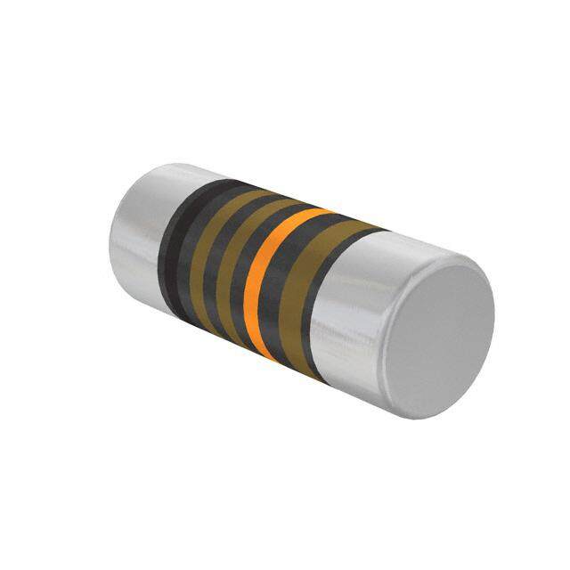
| 描述 | RES 7.5K OHM 1/20W 5% 0201 SMD厚膜电阻器 - SMD 0201 7500ohms 5% Thick Film Resistor |
| 产品分类 | |
| 品牌 | Panasonic |
| 产品手册 | |
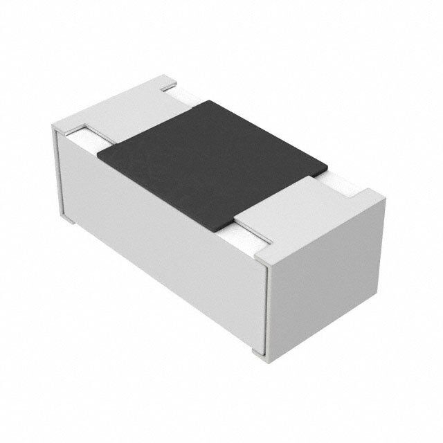
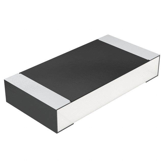
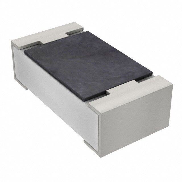
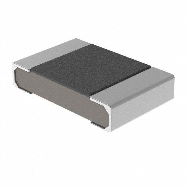
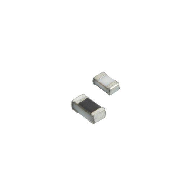
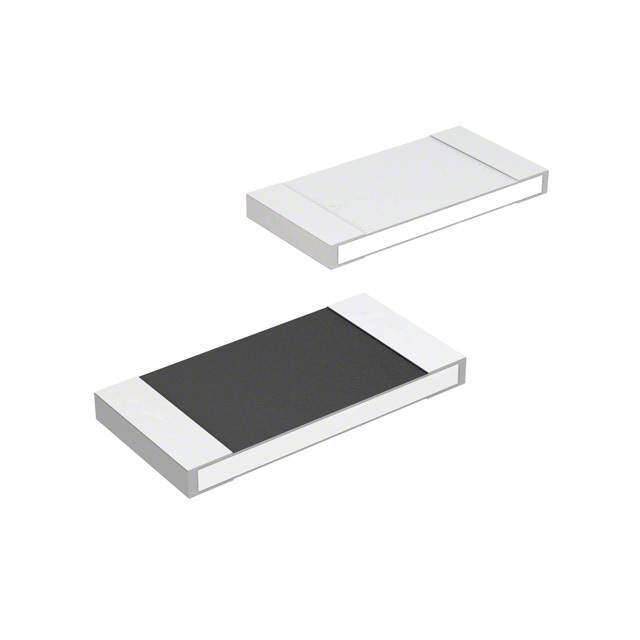
| 产品图片 |
|
| rohs | RoHS 合规性豁免无铅 / 符合限制有害物质指令(RoHS)规范要求 |
| 产品系列 | 薄膜电阻器,厚膜电阻器 - SMD,Panasonic ERJ-1GEJ752CERJ |
| 数据手册 | |
| 产品型号 | ERJ-1GEJ752C |
| 产品 | Thick Film Resistors SMD |
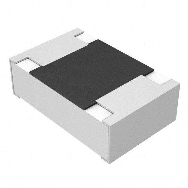
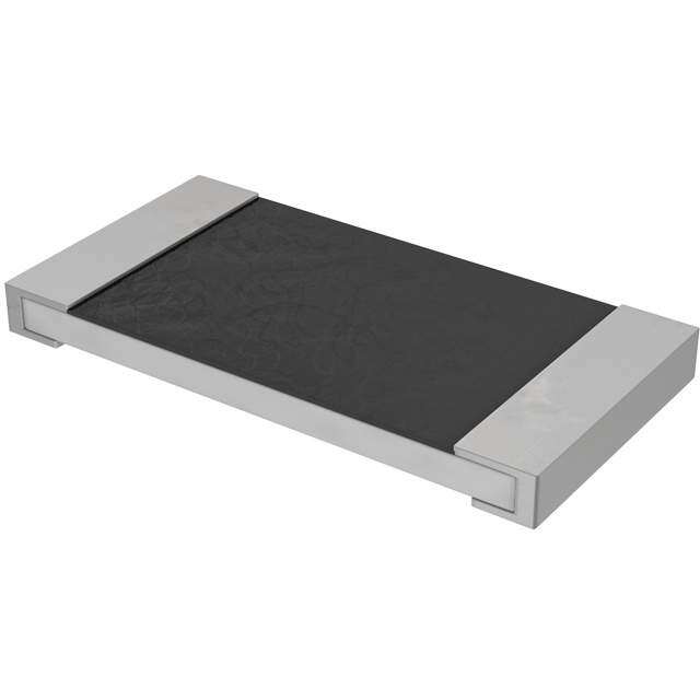
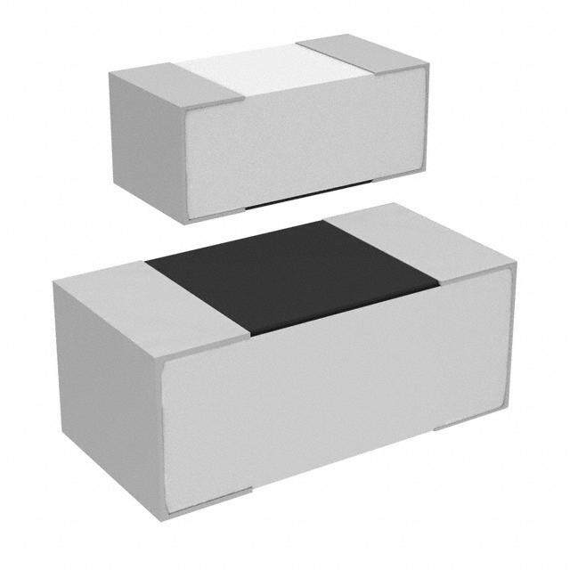
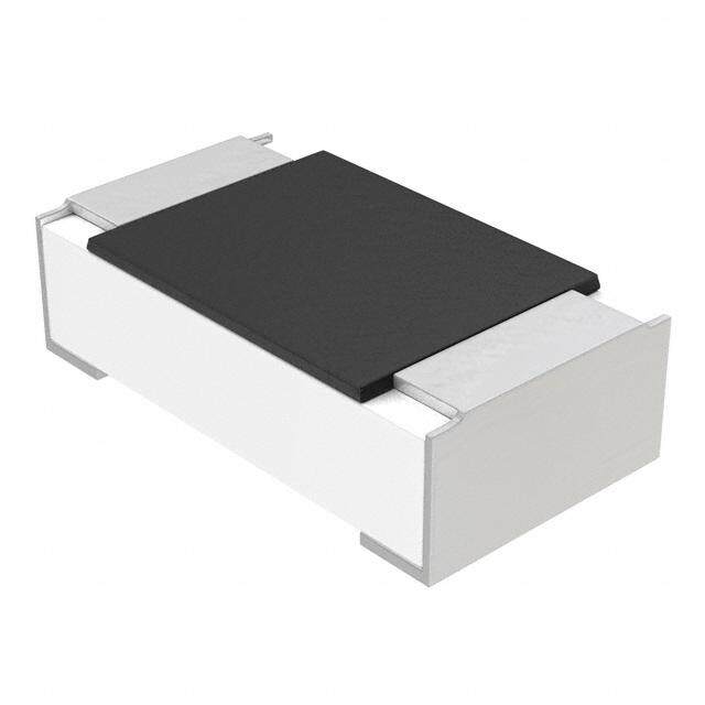
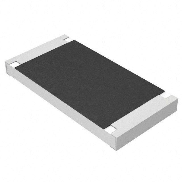
| 产品目录绘图 |
|
| 产品目录页面 | |
| 产品种类 | 厚膜电阻器 - SMD |
| 供应商器件封装 | 0201 |
| 其它名称 | ERJ1GEJ752C |
| 功率(W) | 0.05W,1/20W |
| 功率额定值 | 50 mW |
| 包装 | 带卷 (TR) |
| 商标 | Panasonic |
| 外壳代码-in | 0201 |
| 外壳代码-mm | 0603 |
| 外壳宽度 | 0.3 mm |
| 外壳长度 | 0.6 mm |
| 外壳高度 | 0.23 mm |
| 大小/尺寸 | 0.024" 长 x 0.012" 宽(0.60mm x 0.30mm) |
| 容差 | 5 % |
| 封装 | Reel |
| 封装/外壳 | 0201(0603 公制) |
| 封装/箱体 | 0201 (0603 metric) |
| 工作温度范围 | - 55 C to + 125 C |
| 工具箱 | /product-detail/zh/CR15-KIT/CR15-KIT-ND/4935610 |
| 工厂包装数量 | 15000 |
| 成分 | 厚膜 |
| 标准包装 | 15,000 |
| 温度系数 | 200 PPM / C |
| 特性 | - |
| 电压额定值 | 25 V |
| 电阻 | 7.5 kOhms |
| 电阻(Ω) | 7.5k |
| 端子数 | 2 |
| 类型 | Thick Film Chip Resistors |
| 系列 | ERJ |
| 高度 | 0.010"(0.26mm) |


- 商务部:美国ITC正式对集成电路等产品启动337调查
- 曝三星4nm工艺存在良率问题 高通将骁龙8 Gen1或转产台积电
- 太阳诱电将投资9.5亿元在常州建新厂生产MLCC 预计2023年完工
- 英特尔发布欧洲新工厂建设计划 深化IDM 2.0 战略
- 台积电先进制程称霸业界 有大客户加持明年业绩稳了
- 达到5530亿美元!SIA预计今年全球半导体销售额将创下新高
- 英特尔拟将自动驾驶子公司Mobileye上市 估值或超500亿美元
- 三星加码芯片和SET,合并消费电子和移动部门,撤换高东真等 CEO
- 三星电子宣布重大人事变动 还合并消费电子和移动部门
- 海关总署:前11个月进口集成电路产品价值2.52万亿元 增长14.8%

PDF Datasheet 数据手册内容提取
Thick Film Chip Resistors Thick Film Chip Resistors 01005, 0201, 0402, 0603, 0805, 1206, 1210, 1812, 2010, 2512 Type: ERJ XG, 1G, 2G, 3G, 6G, 8G, 14, 12, 12Z, 1T ■ Features ● Small size and lightweight ● High reliability Metal glaze thick fil m resistive element and three layers of electrodes ● Compatible with placement machines Taping packaging available ● Suitable for both reflo w and fl ow sol deri ng ● Reference Standards IEC 60115-8, JIS C 5201-8, EIAJ RC-2134B ■Explanation of Part Numbers ● ERJXGE, 1GE, 2GE, 3GE, 6GE, 8GE, 14, 12, 12Z, 1T Series, ±5 % type 1 2 3 4 5 6 7 8 9 10 11 12 E R J 3 G E Y J 1 0 2 V ProductCode Size,PowerRating Marking ResistanceTolerance PackagingMethods ThickFilm Type:inches PowerR. Code Marking Code Tolerance Code Packaging ChipResistors XGE:01005 0.031W Y ValueMarkingon J ±5% Y P2rmesmsedpiCtcahrr,ie2r0T0a0p0inpgcs. 1GE:0201 0.05W blackside 0 Jumper (OnlyXGEtype) 2GE:0402 0.063W ✽Nil Nomarking PressedCarrierTaping 3GE:0603 0.1W C 2mmpitch,15000pcs. 6GE:0805 0.125W ResistanceValue (Only1GEtype) 8GE:1206 0.25W Thefirsttwodigitsaresignificantfiguresofresistanceand PunchedCarrierTaping 14:1210 0.25W thethirdonedenotesnumberofzerosfollowing. X 2mmpitch,10000pcs. (Only2GEtype) 12:1812 0.5W DecimalPointisexpressedbyRas4.7=4R7. 12Z:2010 0.5W JumperisexpressedbyR00. V PunchedCarrierTaping (Only3GE,6GE,8GEtype) 1T:2512 1W EmbossedCarrierTaping U (Only14,12,12Z,1Ttype) ✽ When omitted, the rest of the P/N factors shall be moved up respectively. (Only XGE, 1GE, 2GE type) Design and specifi cations are each subject to change without notice. Ask factory for the current technical specific ations before purchase and/or use. Should a safety concern arise regarding this product, please be sure to contact us immediately. Mar. 2005
Thick Film Chip Resistors ■Construction ■Dimensions in mm (not to scale) L a W Protectivecoating Aluminasubstrate Electrode(Inner) t b Type Dimensions (mm) Mass (Weight) (inches) L W a b t (g/1000 pcs.) ERJXG 0.40±0.02 0.20±0.02 0.10±0.03 0.10±0.03 0.13±0.02 0.04 (01005) ERJ1G 0.60±0.03 0.30±0.03 0.10±0.05 0.15±0.05 0.23±0.03 0.15 Electrode (0201) (Between) ERJ2G 1.00±0.05 0.50±0.05 0.20±0.10 0.25±0.05 0.35±0.05 0.8 (0402) ERJ3G 1.60±0.15 0.80+0.15 0.30±0.20 0.30±0.15 0.45±0.10 2 (0603) –0.05 ERJ6G 2.00±0.20 1.25±0.10 0.40±0.20 0.40±0.20 0.60±0.10 4 (0805) ERJ8G 3.20+0.05 1.60+0.05 0.50±0.20 0.50±0.20 0.60±0.10 10 (1206) –0.20 –0.15 Thickfilm Electrode(Outer) E(1R21J104) 3.20±0.20 2.50±0.20 0.50±0.20 0.50±0.20 0.60±0.10 16 resistiveelement ERJ12 4.50±0.20 3.20±0.20 0.50±0.20 0.50±0.20 0.60±0.10 27 (1812) ERJ12Z 5.00±0.20 2.50±0.20 0.60±0.20 0.60±0.20 0.60±0.10 27 (2010) ERJ1T 6.40±0.20 3.20±0.20 0.65±0.20 0.60±0.20 0.60±0.10 45 (2512) ■ Ratings <For Resistor> Limiting Element Maximum Overload Resistance Resistance T.C.R. Category Temperature Type Power Rating Voltage (Maximum Voltage(2) Tolerance Range [(cid:2)10–6/°C Range (Operating (inches) at 70 °C (W) Temperature Range) RCWV)(1) (V) (V) (%) ((cid:1)) (ppm/°C)] (°C) ERJXG <100 (cid:1):±300 (01005) 0.031 15 30 ±5 10 to 1 M (E24) 100 (cid:1)<:±200 –55 to +125 ERJ1G 0.05 15 30 ±5 1 to 10 M (E24) –55 to +125 (0201) ERJ2G <10 (cid:1): 0.063 50 100 ±5 1 to 10 M (E24) –55 to +155 (0402) –100 to +600 ERJ3G 0.1 50 100 ±5 1 to 10 M (E24) –55 to +155 (0603) ERJ6G 0.125 150 200 ±5 1 to 10 M (E24) –55 to +155 (0805) ERJ8G 10 (cid:1) to 1 M(cid:1): 0.25 200 400 ±5 1 to 10 M (E24) –55 to +125 (1206) ±200 ERJ14 0.25 200 400 ±5 1 to 10 M (E24) –55 to +125 (1210) ERJ12 0.5 200 400 ±5 1 to 10 M (E24) –55 to +125 (1812) ERJ12Z 1 M(cid:1)<: (2010) 0.5 200 400 ±5 1 to 10 M (E24) –400 to +150 –55 to +125 ERJ1T 1 200 400 ±5 1 to 1 M (E24) –55 to +125 (2512) (1) Rated Continuous Working Voltage (RCWV) shall be de ter mined from RCWV=(cid:3)Power Rating (cid:2) Res is tance Values, or Limiting Element Voltage (max. RCWV) list ed above, whichever less. (2) Overload (Short-time Overload) Test Voltage (SOTV) shall be de term ined from SOTV=2.5(cid:2)Power Rating or max. Over load Volt age list ed above whiche ve r less. <For Jumper> Power Derating Curve Type Rated Current Maximum Overl oad Current (inches) (A) (A) For resistors operated in ambient temperatures above ERJ1G (0201) 0.5 1 70 °C, power rating shall be derated in accordance ERJ2G (0402) with the fi gure below. 1 2 ERJ3G (0603) –55°C 70°C 100 ERJ6G (0805) %)80 ERJ8G (1206) ad(60 EEERRRJJJ111422Z (((112280111200))) 2 4 RatedLo24000 XG,1G,2G,14,12,121Z2,15T°C3G,165G5,°8CG –60 –40–20 0 20 40 60 80 100120140160180 ERJ1T (2512) AmbientTemperature(°C) Design and specifi cations are each subject to change without notice. Ask factory for the current technical specific ations before purchase and/or use. Should a safety concern arise regarding this product, please be sure to contact us immediately. Mar. 2005
Thick Film Chip Resistors ■ Packaging Methods (Taping) ● Standard Quantity Type Kind of Taping Pitch (P) Quantity 1 ERJXG 20000 pcs./reel Pressed Carrier Taping ERJ1G 2 mm 15000 pcs./reel ERJ2G 10000 pcs./reel ERJ3G Punched Carrier Taping ERJ6G ERJ8G 5000 pcs./reel ERJ14 4 mm ERJ12 Embossed Carrier Taping ERJ12Z ERJ1T 4000 pcs./reel ● Carrier Tape (Unit : mm) Pressed Carrier Punched Carrier Embossed Carrier P1 P2 P0 fD0 E F W B T T T A P1 (2mmpitch) fD1(OnlyEmboss) Type A B W F E P P P fD T fD 1 2 0 0 1 ERJXG 0.25±0.03 0.45±0.03 0.31±0.05 – ERJ1G 0.38±0.05 0.68±0.05 2.00±0.10 0.42±0.05 – ERJ2G 0.70±0.05 1.20±0.05 0.52±0.05 – 8.00±0.20 ERJ3G 1.10±0.10 1.90±0.10 3.50±0.05 0.70±0.05 – ERJ6G 1.65±0.15 2.50±0.20 – 1.75±0.10 2.00±0.05 4.00±0.10 1.50+0.10 0.84±0.05 ERJ8G 2.00±0.15 3.60±0.20 −0 – ERJ14 2.80±0.20 3.50±0.20 8.00±0.30 4.00±0.10 1.0+0.10 −0 ERJ12 3.50±0.20 4.80±0.20 1.00±0.10 ERJ12Z 2.80±0.20 5.30±0.20 12.00±0.30 5.50±0.20 1.5 min. ERJ1T 3.60±0.20 6.90±0.20 ● Taping Reel (Unit : mm) Type fA fB fC W T T ERJXG ERJ1G ERJ2G fC ERJ3G 9.0±1.0 11.4±1.0 Bf ERJ6G 180.0+0 60 min. 13.0±1.0 ERJ8G –3.0 ERJ14 ERJ12 fA W ERJ12Z 13.0±1.0 15.4±2.0 ERJ1T Design and specifi cations are each subject to change without notice. Ask factory for the current technical specific ations before purchase and/or use. Should a safety concern arise regarding this product, please be sure to contact us immediately. Mar. 2005
Thick Film Chip Resistors ■ Recommended Land Pattern In case of fl ow soldering, the land width must be smaller than the Chip Resistor width to control the sold er amount properly. Generally, the land width should be 0.7 to 0.8 times (W) of the width of chip resistor. In case of refl ow soldering, solder amount can be adjusted, therefore the land width should be set to 1.0 to 1.3 times chip resistor width (W). Type Dimensions (mm) (inches) a b c ChipResistor ERJXG(01005) 0.15 to 0.20 0.5 to 0.7 0.20 to 0.25 ERJ1G(0201) 0.3 to 0.4 0.8 to 0.9 0.25 to 0.35 ERJ2G(0402) 0.5 to 0.6 1.4 to 1.6 0.4 to 0.6 c ERJ3G(0603) 0.7 to 0.9 2 to 2.2 0.8 to 1 ERJ6G(0805) 1 to 1.4 3.2 to 3.8 0.9 to 1.4 ERJ8G(1206) 2 to 2.4 4.4 to 5 1.2 to 1.8 a ERJ14(1210) 2 to 2.4 4.4 to 5 1.8 to 2.8 b ERJ12(1812) 3.3 to 3.7 5.7 to 6.5 2.3 to 3.5 ERJ12Z(2010) 3.6 to 4 6.2 to 7 1.8 to 2.8 ERJ1T(2512) 5 to 5.4 7.6 to 8.6 2.3 to 3.5 ■ Recommended Soldering Conditions Recommendations and precautions are described below. ●Recommended soldering conditions for reflo w · Reflo w soldering shall be performed a maximum of two times. · Please contact us for additional information when For soldering (Example : Sn/Pb) used in conditions other than those specifie d. · Please measure the temperature of the terminals Temperature Time and study every kind of solder and printed circuit Preheating 140 °C to 160 °C 60 s to 120 s board for solderability bef ore ac tu al use. Main heating Above 200 °C 30 s to 40 s Peak Peak 235 ± 5 °C max. 10 s ure Preheating For lead-free soldering (Example : Sn/Ag/Cu) at er Temperature Time p m Heating Preheating 150 °C to 180 °C 60 s to 120 s e T Main heating Above 230 °C 30 s to 40 s Peak max. 260 °C max. 10 s Time ●Recommended soldering conditions for flo w For soldering For lead-free soldering Temperature Time Temperature Time Preheating 140 °C to 180 °C 60 s to 120 s 150 °C to 180 °C 60 s to 120 s Soldering 245 ± 5 °C 20 s to 30 s max. 260 °C max. 10 s Safety Precautions The following are precautions for individual products. Please also refer to the precautions common to Fixed Resistors shown on page ER3 of this catalog. 1. Take measures against mechanical stress during and after mounting of Thick Film Chip Resistors (herea f ter called the resistors) so as not to damage their electrodes and protective coatings. 2. If a transient load (heavy load in a short time) like a pulse is expected to be applied, check and evaluate the operations of the resistors when installed in your products before use. Never exceed the rated power. Otherwise, the performance and/or reliability of the resistors may be impaired. 3. Do not use halogen-based or other high-activity fl ux. Otherwise, the residue may impair the resistors' per for mance and/or reliability. 4. When soldering with a soldering iron, never touch the resistors' bodies with the tip of the soldering iron. When using a soldering iron with a high temperature tip, fin ish soldering as quickly as possible (within three seconds at 350 °C max.). 5. As the amount of applied solder becomes larger, the mechanical stress applied to the resistors increases, causing problems such as cracks and faulty characteristics. Avoid applying an excessive amount of solder. 6. Do not apply shock to the resistors or pinch them with a hard tool (e.g. pliers and tweezers). Oth er wise, the re sist ors' protective coatings and bodies may be chipped, affecting their performance. 7. Avoid excessive bending of printed circuit boards in order to protect the resistors from abnormal stress. Design and specifi cations are each subject to change without notice. Ask factory for the current technical specific ations before purchase and/or use. Should a safety concern arise regarding this product, please be sure to contact us immediately. Mar. 2005
Safety Precautions (Common precautions for Fixed Resistors) (cid:127) When using our products, no matter what sort of equipment they might be used for, be sure to make a written agreement on the specific ations with us in advance. The design and specific ations in this catalog are subject to change without prior notice. (cid:127) Do not use the products beyond the specifi cations described in this catalog. (cid:127) This catalog explains the quality and performance of the products as individual components. Be fore use, check and evaluate their operations when installed in your products. (cid:127) Install the following systems for a failsafe design to ensure safety if these products are to be used in equip ment where a defect in these products may cause the loss of human life or other signifi cant damage, such as damage to vehicles (au to mob ile, train, vessel), traffi c lights, medical equipment, aerospace equipment, elec tric heating app lia nc es, com bus tion/gas equipment, rotating equipment, and disaster/crime prevention equipm ent. ✽ Systems equipped with a protection circuit and a protection device ✽ Systems equipped with a redundant circuit or other system to prevent an unsafe status in the event of a single fault (1) Precautions for use (cid:127) These products are designed and manufactured for general and stan dard use in general elec tron ic equipment (e.g. AV equipment, home electric ap plia nc es, offi ce equipment, information and com mu ni ca tion equipment) (cid:127) These products are not intended for use in the following special conditions. Bef ore using the products, care full y check the effects on their quality and performance, and determine whether or not they can be used. 1. In liquid, such as water, oil, chemicals, or organic solvent 2. In direct sunlight, outdoors, or in dust 3. In salty air or air with a high concentration of corrosive gas, such as Cl2, H2S, NH3, SO2, or NO2 4. In an environment where strong static electricity or electromagnetic waves exist 5. In an environment where these products cause dew condensation 6. Sealing or coating of these products or a printed circuit board on which these products are mounted, with resin or other materials (cid:127) These products generate Joule heat when energized. Carefully position these products so that their heat will not affect the other components. (cid:127) Carefully position these products so that their temperatures will not exceed the category temperature range due to the effects of neighboring heat-generating comp o nents. Do not mount or place heat-generating comp on ents or infl ammables, such as vinyl-coated wires, near these products . (cid:127) Note that non-cleaning solder, halogen-based highly active flu x, or water-soluble flu x may deteriorate the performance or reliability of the products. (cid:127) Carefully select a fl ux cleaning agent for use after soldering. An unsuitable agent may deteriorate the performance or reliability. In particular, when using water or a water-soluble cleaning agent, be careful not to leave water res i dues. Otherwise, the insulation performance may be deteriorated. (2) Precautions for storage The performance of these products, including the solderability, is guaranteed for a year from the date of arrival at your company, provided that they remain packed as they were when delivered and stored at a temperature of 5 °C to 35 ° C and a relative humidity of 45 % to 85 %. Even within the above guarantee periods, do not store these products in the fol low ing conditions. Otherwise, their elect ri cal performance and/or solderability may be deteriorated, and the packaging materials (e.g. tapi ng mat er i als) may be def ormed or deteriorated, resulting in mounting failures. 1. In salty air or in air with a high concentration of corrosive gas, such as Cl2, H2S, NH3, SO2, or NO2 2. In direct sunlight <Package markings> Package markings include the product number, quantity, and country of origin. In principle, the country of origin should be indicated in English. Mar. 2005 – ER3 –