 Datasheet下载
- 型号: ERG-2SJ162
- 制造商: Panasonic Corporation
- 库位|库存: xxxx|xxxx
- 要求:
| 数量阶梯 | 香港交货 | 国内含税 |
| +xxxx | $xxxx | ¥xxxx |
查看当月历史价格
查看今年历史价格
ERG-2SJ162产品简介:
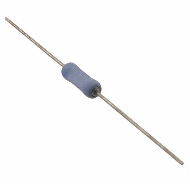
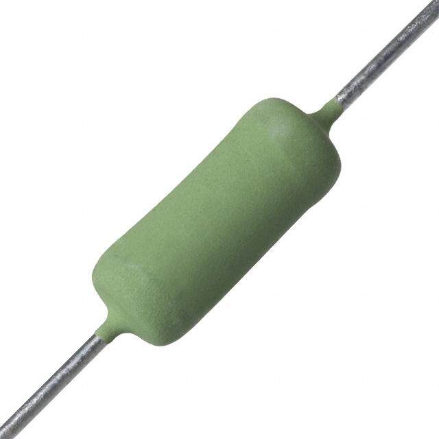
ICGOO电子元器件商城为您提供ERG-2SJ162由Panasonic Corporation设计生产,在icgoo商城现货销售,并且可以通过原厂、代理商等渠道进行代购。 ERG-2SJ162价格参考¥0.32-¥2.65。Panasonic CorporationERG-2SJ162封装/规格:通孔电阻器, 1.6 kOhms ±5% 2W 轴向 通孔电阻器 耐燃,安全 金属氧化物薄膜。您可以下载ERG-2SJ162参考资料、Datasheet数据手册功能说明书,资料中有ERG-2SJ162 详细功能的应用电路图电压和使用方法及教程。
Panasonic Electronic Components(松下电子元件)生产的通孔电阻器型号ERG-2SJ162是一款金属氧化膜电阻器,具有高精度、低噪声和良好的稳定性。其应用场景主要包括以下领域:

 1. 工业控制设备
   - 用于工业自动化设备中的信号调节电路,例如PLC(可编程逻辑控制器)、变频器和伺服驱动器。
   - 在温度、压力或流量传感器的信号调理电路中提供分压或限流功能。

 2. 电源管理
   - 在开关电源(SMPS)或线性电源中用作分压电阻、限流电阻或反馈网络的一部分。
   - 适用于电压检测电路,确保输出电压稳定。

 3. 通信设备
   - 应用于通信基站、路由器和交换机等设备中的滤波电路和信号匹配电路。
   - 用于射频(RF)电路中的阻抗匹配,以减少信号反射和提高传输效率。

 4. 消费电子产品
   - 在音频设备(如放大器、扬声器)中用作音量控制或信号衰减。
   - 用于家用电器(如洗衣机、空调)的控制电路中,实现定时、调速等功能。

 5. 汽车电子
   - 在汽车电子控制系统中,如发动机控制单元(ECU)、车身控制模块(BCM)中用作分压或限流元件。
   - 适用于车灯亮度调节、雨刷速度控制等电路。

 6. 测试与测量仪器
   - 用于万用表、示波器等测量仪器中的输入保护电路或分压网络。
   - 在精密测量设备中提供稳定的电阻值,确保测量结果准确。

 7. 医疗设备
   - 在监护仪、超声波设备等医疗仪器中用作信号处理电路的一部分。
   - 提供稳定的电阻特性,以保证设备运行的安全性和可靠性。

 特性优势
- 高精度:适合需要精确电阻值的应用场景。
- 低噪声:适用于对信号质量要求较高的电路。
- 耐高温:能够在恶劣环境下保持性能稳定。
- 长期稳定性:适合长时间运行的设备。

总之,ERG-2SJ162凭借其优异的性能,广泛应用于对电阻器性能要求较高的各类电子设备中。
| 参数 | 数值 |
| 产品目录 | |
| 描述 | RES 1.6K OHM 2W 5% AXIAL |
| 产品分类 | |
| 品牌 | Panasonic Electronic Components |
| 数据手册 | http://industrial.panasonic.com/www-cgi/jvcr13pz.cgi?E+PZ+3+AOA0018+ERG2SJ162+7+WW |
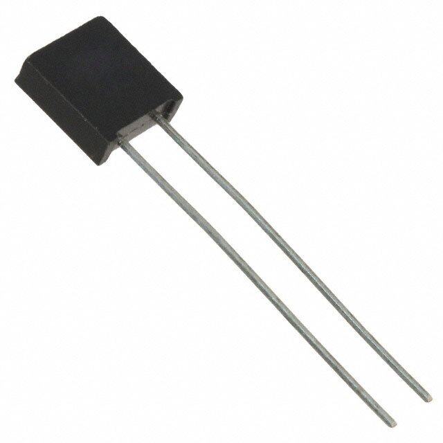
| 产品图片 |
|
| 产品型号 | ERG-2SJ162 |
| rohs | 无铅 / 符合限制有害物质指令(RoHS)规范要求 |
| 产品系列 | ERG |
| 产品目录页面 | |
| 供应商器件封装 | 轴向 |
| 其它名称 | ERG2SJ162 |
| 功率(W) | 2W |
| 包装 | 散装 |
| 大小/尺寸 | 0.157" 直径 x 0.472" 长(4.00mm x 12.00mm) |
| 容差 | ±5% |
| 封装/外壳 | 轴向 |
| 成分 | 金属氧化物薄膜 |
| 标准包装 | 100 |
| 温度系数 | ±350ppm/°C |
| 特性 | 耐燃 |
| 电阻(Ω) | 1.6k |
| 端子数 | 2 |
| 高度 | - |


- 商务部:美国ITC正式对集成电路等产品启动337调查
- 曝三星4nm工艺存在良率问题 高通将骁龙8 Gen1或转产台积电
- 太阳诱电将投资9.5亿元在常州建新厂生产MLCC 预计2023年完工
- 英特尔发布欧洲新工厂建设计划 深化IDM 2.0 战略
- 台积电先进制程称霸业界 有大客户加持明年业绩稳了
- 达到5530亿美元!SIA预计今年全球半导体销售额将创下新高
- 英特尔拟将自动驾驶子公司Mobileye上市 估值或超500亿美元
- 三星加码芯片和SET,合并消费电子和移动部门,撤换高东真等 CEO
- 三星电子宣布重大人事变动 还合并消费电子和移动部门
- 海关总署:前11个月进口集成电路产品价值2.52万亿元 增长14.8%
PDF Datasheet 数据手册内容提取
Metal (Oxide) Film Resistors Metal (Oxide) Film Res is tors Type: ERG(X)S (Small size) (0.5 W, 1 W, 2 W, 3 W, 5 W) ERG(X)F (Anti-heat conducting for PCB) (1 W, 2 W, 3 W, 5 W) Features ● Miniaturized 50 % smaller compared to existing models ● Non-fl ammable ● High Reliability ● Automatic Insertion ● Reference Standards IEC 60115-2, IEC 60115-4, JIS C 5201-4, EIAJ RC-2138 ● RoHS compliant Explanation of Part Numbers Ex.1 : ERX type 1 2 3 4 5 6 7 8 9 10 11 12 E R X 2 S Z J W 1 R 0 E Product Code Power Rating at 70 °C Style · Specification Resistance Resistance Value ERX MReetsails Ftoilrms 112 01.5 W W S S0.m5 aWll tsoi z5e W JTolera±n5c e% Tohf ere fisrisstta tnwcoe d aignidts t haere t hsiirgdn oifincea ndte fingouteress 2 2 W Small size Anti-heat G ±2 % number of zeros following. 35 35 WW F c(Foen dleuacdt inwgir ety)pe D(Eexc.)i m1aRl0 p :o 1in.0t iΩs expressed by 1 W to 5 W “Z” is added according to resistance. The matrix of forming and packaging is as shown in the table below. Resistance Resistance Value Range (Ω) Forming & Taping matrix Part No. Tolerance ERX□□SZ ERX□□S Code Forming / Packaging 12S 1S 2S 3S 5S 1F 2F 3F 5F ±5 % 0.10 to 0.18 0.20 to 9.1 □···□ Straight lead wire type ○ ○ ○ ○ ○ ○ ○ ○ ○ E R X12S ±2 % 0.10 to 0.91 1.0 to 9.1 □···P Cut & Forming type ○ ○ ○ ○ ○ ERX1S ±5 % 0.10 to 0.18 0.20 to 9.1 □···V Axial taping type (Straight lead) ○ ○ ○ ○ ○ ○ ○ ○ ○ ○ ERX1F ±2 % 0.10 to 0.91 1.0 to 9.1 U···V Axial taping type (Stand off) ERX2S ±5 % 0.10 to 0.20 0.22 to 9.1 □···E Radial taping type (E type) ○ ○ ○ ○ ○ ○ ○ ERX2F ±2 % 0.10 to 0.91 1.0 to 9.1 W···E Radial taping type (WE type) ERX3S ±5 % 0.10 to 0.20 0.22 to 9.1 □··H Cut & Forming type ○ ○ ○ ○ ○ ○ ○ ERX3F ±2 % 0.10 to 0.91 1.0 to 9.1 S···E Radial taping type (SE type) ERX5S ±5 % — 0.33 to 9.1 ERX5F ±2 % 1.0 to 9.1 The above example 1 shows a small metal film resistor, 2 W power rating, resistance value of 1.0 Ω, tolerance ±5 %, and package of radial taping. Ex.2 : ERG type 1 2 3 4 5 6 7 8 9 10 11 12 E R G 2 S J W 1 0 3 E Product Code Power Rating at 70 °C Style · Specification Resistance Resistance Value Metal Oxide 12 0.5 W Small size Tolerance The first two digits are significant figures ERG S Film Resistors 1 1 W 0.5 W to 5 W J ±5 % of resistance and the third one denotes 2 2 W Small size Anti-heat G ±2 % number of zeros following. 3 3 W conducting type Decimal point is expressed by 5 5 W F (Fe lead wire) (Ex.) 103 : 10 kΩ 1 W to 5 W The matrix of forming and packaging is as shown in the table below. Forming & Taping matrix Code Forming / Packaging 12S 1S 2S 3S 5S 1F 2F 3F 5F □□□·········□PV SCAtxuriata i&lg t haFtpo lirenmagdi nt ygwp itreye(p Steytrpaeight lead) ○○○ ○○○○ ○○○○ ○○○○ ○○ ○○ ○○ ○○ ○ □U······VE ARxaidaila tla tpaipnign gty tpyep(eS(tEa ntydp oef)f) ○ ○ ○ ○ ○ ○ ○ W···E Radial taping type(WE type) □···H Cut & Forming type ○ ○ ○ ○ ○ ○ ○ ○ S···E Radial taping type(SE type) The above example 2 shows a small metal oxide film resistor, 2 W power rating, resistance value of 10 kΩ, tolerance ±5 %, and package of radial taping. Design and specifications are each subject to change without notice. Ask factory for the current technical specifications before purchase and/or use. Should a safety concern arise regarding this product, please be sure to contact us immediately. 02 Sep. 2014
Metal (Oxide) Film Resistors Construction Dimensions in mm (not to scale) Lead wire k L k fD HHiigghh rreelliiaabbllee mmeettaall poxlaidtien gfi lfim lm (ERG) ( SF ttyyppee :: FCeu wwiirree) fd (ERX) Dimensions (mm) Mass Part No. (Weight) C(Heigrahm tihce cr morael cond uc tivi ty) L 0D k 0d [g/pc.] ERG(X)12S 6.35+–00..6355 2.3+–00..35 30.0±3.0 0.65±0.05 0.26 Spi ral ling turns Marking ERG(X)1S 0.65±0.05 ERG(X)1F 9.00+–11..5000 2.8±0.5 30.0±3.0 0.80±0.05 0.33 ERG(X)2S ERG(X)2F 12.00+–11..0500 4.0±1.0 30.0±3.0 0.80±0.05 0.66 ERG(X)3S 15.00±1.50 5.5±1.0 38.0±3.0 0.80±0.05 1.47 Flame and solvent retardant ERG(X)3F ERG(X)5S End cap 24.00±1.50 8.0±1.0 38.0±3.0 0.80±0.05 3.54 ERG(X)5F Ratings Maximum Dielectric Power Limiting Maximum IntermittentWith stand ing Res. Resistance Standard Part No. Rating Element Overload Overload Voltage Tol. Range (Ω)(5) T.C.R. Resistance at 70 °C Voltage(1) Voltage(2) (×10–6/°C) Voltage(3) (%)(4) Value (W) (V) (V) (V) (VAC) min.(6) max. G (±2) 1 22 k ERG(X)12S 0.5 300 600 600 350 ±350 E24 J (±5) 0.2 47 k ERG(X)1S G (±2) 1 68 k 1 350 600 600 350 ±350 E24 ERG(X)1F J (±5) 0.2 100 k ERG(X)2S G (±2) 1 100 k 2 350 700 1000 600 ±350 E24 ERG(X)2F J (±5) 0.22 100 k ERG(X)3S G (±2) 1 100 k 3 350 700 1000 1000 ±300 E24 ERG(X)3F J (±5) 0.22 100 k ERG(X)5S G (±2) 1 100 k 5 500 1000 1500 1000 ±200 E24 ERG(X)5F J (±5) 0.33 100 k (1) Rated Continuous Working Voltage (RCWV) shall be determined (4) Resistance tolerance is of use besides range listed, please inquire. from RCWV=√Power Rating×Resistance Value or Limiting Element (5) Resistance Range Type ERG : >10 Ω Voltage listed above whichever less. Type ERX : <9.1 Ω (2) Overload (Short-time Overload) Test Voltage (SOTV) shall be (6) As for the low resistance value range, "Z" is given to the part determined from SOTV=2.5×Power Rating or max. Overload number. (Refer to the explanation of part numbers.) Voltage listed above whichever less. (3) Intermittent Overload Test Voltage (IOTV) shall be determined from IOTV=4.0×Power Rating or max. Intermittent Overload Voltage listed above whichever less. ✽ Z type is non standard resistance values. CodePart No.Res.Tol.Res. Value Range CodePart No.Res.Tol.Res. Value Range ±2 % 0.1 to 0.91 Ω 2S ±2 % 0.1 to 0.91 Ω 12S ±5 % 0.1 to 0.18 Ω 2F ±5 % 0.1 to 0.2 Ω Z Z 1S ±2 % 0.1 to 0.91 Ω 3S ±2 % 0.1 to 0.91 Ω 1F ±5 % 0.1 to 0.18 Ω 3F ±5 % 0.1 to 0.2 Ω Power Derating Curve 120 For resistors operated in ambient temperatures above –55 °C 70 °C 100 70 °C, power rating shall be derated in accordance %) with the figure on the right. d ( 80 ERG(X)1S, 1F a o 60 ERG(X)2S, 2F L d ERG(X)12S ERG(X)3S, 3F e 40 at ERG(X)5S, 5F R 20 130 °C 235 °C 0 –60 –40–20 0 20 40 60 80 100120140160180200220240 Ambient Temperature (°C) Design and specifications are each subject to change without notice. Ask factory for the current technical specifications before purchase and/or use. Should a safety concern arise regarding this product, please be sure to contact us immediately. 02 Sep. 2014
Metal (Oxide) Film Resistors Packaging Methods Taped & Box Stand-off Taped & Box ERG(X)□□S□□□□V ERG(X)□□S□U□□□V 6.0±0.5 d f fd P W1 P H H crush width 0.8 mm (1 W) W 1.1 mm (2 W, 3 W) W Standard Taping (mm) Box (mm) Part Number Quantity (pcs./box) P 50×P W H W1 0d a b c ERG(X) 12S□□□□□V 2,000 5.0±0.3 250±2 52.0±1.5 — — 0.65±0.05 85 80 255 b ERG(X) 1S□□□□□V — — 2,000 5.0±0.3 250±2 52.0±1.5 0.65±0.05 85 80 255 EERRGG((XX)) 21SS□□□U□□□□□□VV 12—.0– 20.01.2—0+ 00.15 Marking c 1,000 5.0±0.3 250±2 52.0±1.5 0.80±0.05 85 80 255 ERG(X) 2S□U□□□V 15.5 – 20.01.40+ 00.15 a ERG(X) 3S□□□□□V — — 1,000 10.0±0.5 500±2 74.0±2.0 0.80±0.05 105 100 325 ERG(X) 3S□U□□□V 23.0 – 20.0 1.4+00.15 Cut & Formed Type ERG(X)□□S□□□□P Standard Dimensions (mm) Part Number Quantity (pcs./box) L 0D S h h2 SL f 0.65±0.05 (0.5 W, 1 W)f 0.80±0.05 (2 W, 3 W, 5 W) fD 0.8hh (20Uo.f5p P pWWe,r 1bs ouWarf)radce EEERRRGGG(((XXX))) 1212SSS□□□□□□□□□□□□PPP 111,,,000000000 1692..30.0500++––+–011011....6503..50500500 224...380+±±–0010....5503 111025...050±±±111...555 446...000±±±111...555 444...000±±±111...555 1.2±0.2 (0.15. 0W (,2 1 W W, )3 W, 5 W) ERG(X) 3S□□□□P 1,000 15.00±1.50 5.5±1.0 20.0±2.0 6.5±1.5 4.0±1.5 1.4±0.2 (2 W, 3 W, 5 W) ERG(X) 5S□□□□P 500 24.00±1.50 8.0±1.0 30.0±2.0 7.5±1.5 4.0±1.5 ERG(X)□F□□□□H Standard Dimensions (mm) Part Number Quantity (pcs./box) L 0D S h h2 SL fD ERG(X)1F□□□□H 1,000 9.0+–11..50 2.8±0.5 12.5±1.5 8±2 4.0±1.5 f 0.80±0.05 ERG(X)2F□□□□H 1,000 12.0+–11..50 4.0±1.0 15.0±1.5 6±2 5.0±1.5 Upper surface h of PW board ERG(X)3F□□□□H 1,000 15.0±1.5 5.5±1.0 20.0±2.0 10±2 5.0±1.5 h2 1.0 1.4±0.2 ERG(X)5F□□□□H 500 24.0±1.5 8.0±1.0 30.0±2.0 10±2 5.0±1.5 Design and specifications are each subject to change without notice. Ask factory for the current technical specifications before purchase and/or use. Should a safety concern arise regarding this product, please be sure to contact us immediately. 02 Sep. 2014
Metal (Oxide) Film Resistors Packaging Methods For Panasert Au to mati c Insertion Machine Radial Taped & Box ERG(X)□□S□□□□E (12S, 1S, 2S) Insulated P P2 Lead fD A F P1 H1 H0 W1 fd W P0 fD0 Dimensions (mm) Dimensions (mm) Dimensions (mm) Dimensions (mm) Dimensions (mm) P 12.7±1.0 W 18.0±0.5 12S 32 max. 12S 6.35+–00..6355 12S 2.3+–00..53 P0 12.7±0.3 W1 9.0±0.5 H1 1S 32 max. A 1S 9.0+–11..50 0D 1S 2.8±0.5 P1 3.85±0.70 2S 38 max. 2S 12.0+–11..50 2S 4.0±1.0 P2 6.35±1.00 H0 16.0±0.5 0d 0.65±0.05 F 5.0±0.8 0D0 4.0±0.2 ● Radial Tape Package Specifi cations Dimensions (mm) Standard Quantity Part Number (pcs./box) a b c ERG(X) 12S□□□□E 46 130 335 2,000 ERG(X) 1S□□□□E 46 130 335 2,000 b ERG(X) 2S□□□□E 49 100 335 1,000 Marking a c For Panasert Automatic Insertion Machine Radial Taped & Box ERG(X)□□S□W□□□E (12S, 1S, 2S, 3S) Dimensions (mm) Dimensions (mm) 12S 12.7±1.0 0D0 12S, 1S, 2S, 3S 4.0±0.2 P P1 P 1S, 2S, 3S 30.0±1.0 12S 6.35+–00..3655 12S 12.7±0.3 1S 9.0+–11..50 P0 1S, 2S, 3S 15.0±0.3 A 2S 12.0+–11..50 A B 12S 6.35±1.00 3S 15.0±1.5 D P1 f 1S, 2S, 3S 7.5±1.0 12S 11.2 max. H1 P2 12S 3.85±0.70 B 1S 14.0 max. 1S, 2S, 3S 3.75±0.50 2S 17.0 max. 12S 5.0±0.5 3S 21.0 max. P2 F H0 F 1S, 2S, 3S 7.5±0.8 12S 2.3+–00..53 W 12S, 1S, 2S, 3S 18.0±0.5 1S 2.8±0.5 W1 W1 12S, 1S, 2S, 3S 9.0±0.5 0D 2S 4.0±1.0 W 12S 16.0±0.5 3S 5.5±1.0 fd H0 1S, 2S 18.0±1.0 0d 12S 00.65±0.05 3S 19.0±1.0 1S, 2S, 3S 00.80±0.05 12S 6.5+00.6 P0 fD0 H1 1S, 2S 6.5+10.0 3S 8.0+1 0.0 Design and specifications are each subject to change without notice. Ask factory for the current technical specifications before purchase and/or use. Should a safety concern arise regarding this product, please be sure to contact us immediately. 02 Sep. 2014
Metal (Oxide) Film Resistors Packaging Methods For Panasert Automatic Insertion Machine Radial Taped & Box ERG(X)□F□S□□□E (1F, 2F, 3F) Dimensions (mm) Dimensions (mm) P1 P P 30.0±1.0 H2 1.0±0.3 A B P0 15.0±0.3 0D0 4.0±0.2 D P1 7.5±1.0 1F 9.0+–11..05 f H2 F H1 P2 3.75±0.50 A 2F 12.0+–11..05 F 7.5±0.8 3F 15.0±1.5 P2 H0 W 18.0±0.5 1F 14 max. W1 W1 9.0±0.5 B 2F 17 max. fd fD0 W H0 1F 16.0+ 10.07.0+10.0 31FF 221.8 m±0a.x5. P0 H1 2F 8.0+10.0 0D 2F 4.0±1.0 3F 9.0+10.0 3F 5.5±1.0 0d 0.80±0.05 ● Radial Tape Package Specifi cations Dimensions (mm) Standard Quantity Part No. (pcs./box) a b c ERG(X) 12S□ W□□□E 46 145 325 2,000 ERG(X) 1S□ W□□□E 49 150 317 1,000 ERG(X) 1F□ S□□□E ERG(X) 2S□ W□□□E 49 150 317 500 b ERG(X) 2F□ S□□□E ERG(X) 3F□ S□□□E 49 190 315 500 Marking a c Design and specifications are each subject to change without notice. Ask factory for the current technical specifications before purchase and/or use. Should a safety concern arise regarding this product, please be sure to contact us immediately. 02 Sep. 2014
Metal (Oxide) Film Resistors Hot-spot Temperature (for Reference) The temperature of the resistor body increases with the curve below. A touching vinyl wire may cause damages to resistor element. Do not place vinyl wires around resistors and be sure to consider where the resistors will be placed. Measuring position A B +250 +250 +200 +200 2F-A △T (°C)+150 △T (°C)+150 2S-A perature+100 1S-A perature+100 2S-B m m Te 1S-B Te 2F-B 12S-A +50 12S-B +50 0 25 50 75 100 0 25 50 75 100 Rated Load (%) Rated Load (%) +250 +250 3F-A 5F-A +200 +200 5S-A 3S-A C) C) △T (°+150 △T (°+150 perature+100 3S-B perature+100 5S-B m m Te 3F-B Te 5F-B +50 +50 0 25 50 75 100 0 25 50 75 100 Rated Load (%) Rated Load (%) Safety Precautions The following are precautions for individual products. Please also refer to the common precautions for Fixed Resistors in this catalog. 1. Transient voltage If there is a possibility that the transient phenomenon (significantly high voltage applied in a short time) may occur or that a high voltage pulse may be applied, make sure to evaluate and check the characteristics of Metal(Oxide) Film Resistors (hereafter called the resistors) mounted on your product rathe r than only depending on the calculated powe r limit or steady-state conditions to complete the design or decide to use the resistors. 2. The resistors are covered with a special coating. Do not apply shock or vibration to them, or pinch them with long-nose pliers. Otherwise, the resistors may be damaged. 3. Do not apply excessive tension to the lead-connecte d sections. When bending the lead wire, do not apply excessive stress to the resistors and provide the wire with a natural curvature. 4. Do not brush the resistors during or after the cleaning process, which may be conducted after soldering. Otherwise, the coating film may be damaged. Design and specifications are each subject to change without notice. Ask factory for the current technical specifications before purchase and/or use. Should a safety concern arise regarding this product, please be sure to contact us immediately. 02 Sep. 2014
Metal (Oxide) Film Resistors (Data for Reference) Pulse Char ac ter is tics (Usual) P : Pulse limit power (W) P V : Pulse limit voltage (V) P t : Pulse continuous time (s) PP (VP) T : Period (s) V : Rated voltage (V) R P : Rated power (W) R : Resistance value (Ω) t V : Max. pulse limit volta ge (V) p max. T Withstand pulse limit power is calculated by the next method. Part No. K Vp max. (V) P = K·P·T/t P V =√K·P·R·T/t ERG(X) 12S 0.5 600 P Reference to the right about a fixed number of V ERG(X) 1S 0.5 600 P max. ERG(X) 2S 0.5 700 ERG(X) 3S 0.5 700 ● T>1(s) → T=1(s) ● T/t>100 → T/t=100 ERG(X) 5S 0.5 1000 ● P <P → P stands for P (VP <V → V stands forP V ) P R R P ● Added voltage<V p max. ● P or V is referent value P P Conditions: Pulse added time=1000 h Resistance change=±5 % Room temperature Design and specifications are each subject to change without notice. Ask factory for the current technical specifications before purchase and/or use. Should a safety concern arise regarding this product, please be sure to contact us immediately. 02 Sep. 2014