ICGOO在线商城 > 电阻器 > 芯片电阻 - 表面安装 > ERA-6YEB122V

 Datasheet下载
- 型号: ERA-6YEB122V
- 制造商: Panasonic Corporation
- 库位|库存: xxxx|xxxx
- 要求:
| 数量阶梯 | 香港交货 | 国内含税 |
| +xxxx | $xxxx | ¥xxxx |
查看当月历史价格
查看今年历史价格
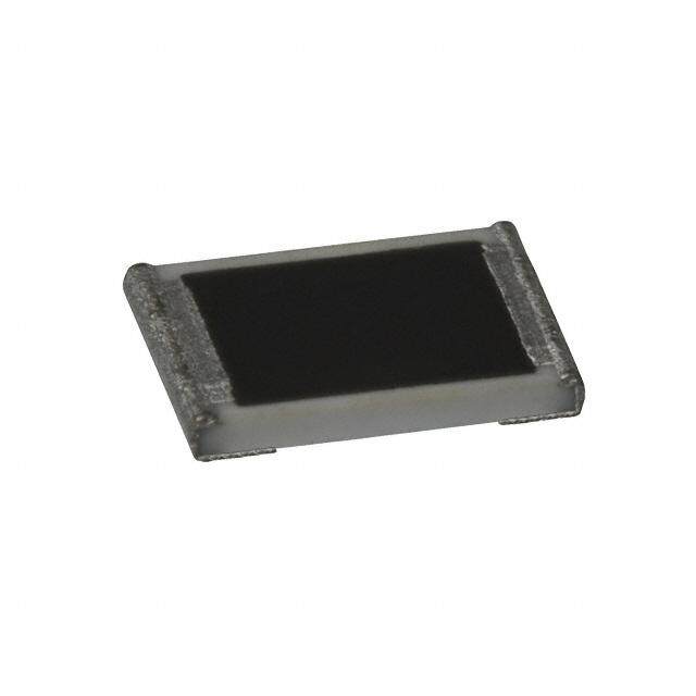
ERA-6YEB122V产品简介:
ICGOO电子元器件商城为您提供ERA-6YEB122V由Panasonic Corporation设计生产,在icgoo商城现货销售,并且可以通过原厂、代理商等渠道进行代购。 ERA-6YEB122V价格参考¥0.66-¥0.66。Panasonic CorporationERA-6YEB122V封装/规格:芯片电阻 - 表面安装, 1.2 kOhms ±0.1% 0.125W,1/8W 薄膜 芯片电阻 0805(2012 公制) 薄膜。您可以下载ERA-6YEB122V参考资料、Datasheet数据手册功能说明书,资料中有ERA-6YEB122V 详细功能的应用电路图电压和使用方法及教程。
Panasonic Electronic Components的ERA-6YEB122V是一款表面贴装的芯片电阻,阻值为1.2kΩ(122表示1200Ω),属于高精度、小型化电阻器,适用于高密度电子电路设计。该型号具有良好的稳定性、耐热性和抗湿性,广泛应用于以下场景:

1. 消费电子产品:如智能手机、平板电脑、笔记本电脑等便携设备中的电源管理、信号调节电路中。

2. 通信设备:用于路由器、交换机、基站模块等通信基础设施中的信号处理和电源控制电路。

3. 工业控制设备:如PLC、传感器模块、工业自动化设备中的精密测量与控制电路。

4. 汽车电子系统:包括车载信息娱乐系统、ECU(电子控制单元)、车载充电模块等,适用于对稳定性和可靠性要求较高的环境。

5. 医疗电子设备:用于便携式或精密医疗仪器中的信号采集与处理电路。

该电阻采用标准贴片封装(通常为1206或相近尺寸),适合自动化贴装工艺,适用于需要高稳定性和高精度的电路设计。
| 参数 | 数值 |
| 产品目录 | |
| 描述 | RES 1.2K OHM 1/8W .1% 0805 SMD薄膜电阻器 - SMD 0805 1.2Kohm 1/10W .1% 25ppm |
| 产品分类 | |
| 品牌 | Panasonic Electronic Components |
| 产品手册 | |
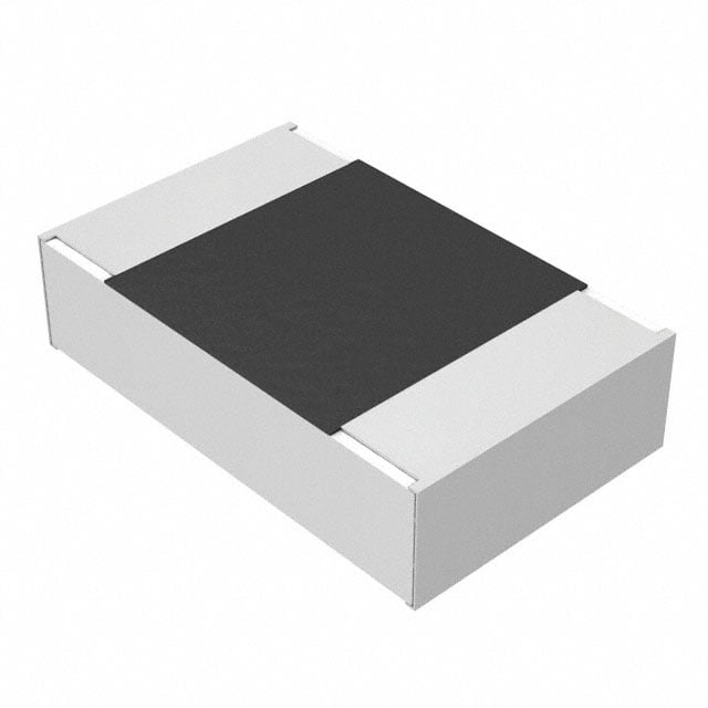
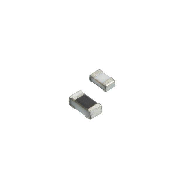
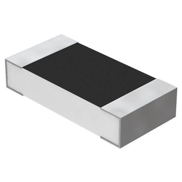
| 产品图片 |
|
| rohs | RoHS 合规性豁免无铅 / 符合限制有害物质指令(RoHS)规范要求 |
| 产品系列 | 薄膜电阻器,薄膜电阻器 - SMD,Panasonic ERA-6YEB122VERA-6Y |
| 数据手册 | |
| 产品型号 | ERA-6YEB122V |
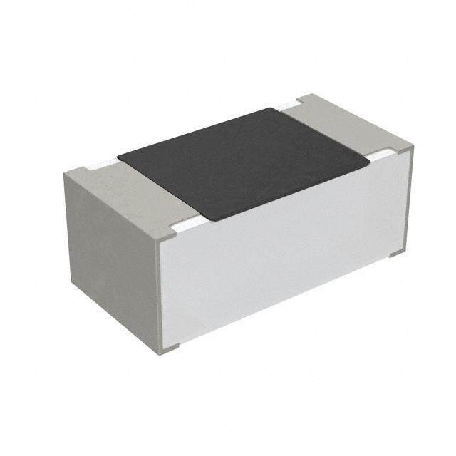
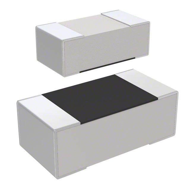
| 产品目录绘图 |
|
| 产品目录页面 | |
| 产品种类 | 薄膜电阻器 - SMD |
| 供应商器件封装 | 0805 |
| 其它名称 | ERA6YEB122V |
| 功率(W) | 0.125W,1/8W |
| 功率额定值 | 100 mW |
| 包装 | 带卷 (TR) |
| 商标 | Panasonic |
| 外壳代码-in | 0805 |
| 外壳代码-mm | 2012 |
| 外壳宽度 | 1.25 mm |
| 外壳长度 | 2 mm |
| 外壳高度 | 0.5 mm |
| 大小/尺寸 | 0.079" 长 x 0.049" 宽(2.00mm x 1.25mm) |
| 容差 | ±0.1% |
| 封装 | Reel |
| 封装/外壳 | 0805(2012 公制) |
| 封装/箱体 | 0805 (2012 metric) |
| 工作温度范围 | - 55 C to + 125 C |
| 工厂包装数量 | 5000 |
| 成分 | |
| 标准包装 | 5,000 |
| 温度系数 | ±25ppm/°C |
| 特性 | - |
| 电压额定值 | 100 V |
| 电阻 | 1.2 kOhms |
| 电阻(Ω) | 1.2k |
| 端子数 | 2 |
| 类型 | Metal Film Chip Resistors |
| 系列 | ERA-6Y |
| 高度 | 0.024"(0.60mm) |


- 商务部:美国ITC正式对集成电路等产品启动337调查
- 曝三星4nm工艺存在良率问题 高通将骁龙8 Gen1或转产台积电
- 太阳诱电将投资9.5亿元在常州建新厂生产MLCC 预计2023年完工
- 英特尔发布欧洲新工厂建设计划 深化IDM 2.0 战略
- 台积电先进制程称霸业界 有大客户加持明年业绩稳了
- 达到5530亿美元!SIA预计今年全球半导体销售额将创下新高
- 英特尔拟将自动驾驶子公司Mobileye上市 估值或超500亿美元
- 三星加码芯片和SET,合并消费电子和移动部门,撤换高东真等 CEO
- 三星电子宣布重大人事变动 还合并消费电子和移动部门
- 海关总署:前11个月进口集成电路产品价值2.52万亿元 增长14.8%


PDF Datasheet 数据手册内容提取
2016 CATALOG Fixed Resistors 2016.4 industrial.panasonic.com/
Fixed Resistors CONTENTS Classifi cation Product Item Part No. Page Safety Precautions (Common precautions for Fixed Resistors) 2 Thick Film Chip Resistors ERJ XG, 1G, 2G, 3G, 6G, 8G, 14, 12, 12Z, 1T 3 Chip Resistors Precision Thick Film Chip Resistors ERJ XG, 1G, 1R, 2R, 3R, 6R, 3E, 6E, 8E, 14, 12, 1T 5 Metal Film (Thin Film) Chip Resistors, ERA 1A, 2A, 3A, 6A, 8A 8 High High Reliability Type Precision Metal Film (Thin Film) Chip Resistors, ERA 2H 11 High Sound Quality Type ERJ 2LW, 3LW, 6LW, 2BW,3BW,6BW,8BW,6CW,8CW Thick Film Chip Resistors ERJ 2B, 3B, 6D, 6B, 8B, 14B, 3R, 6R, 8R, 14R, 12R,12Z, 13 / Low Resistance Type ERJ 1TR, L03, L06, L08, L14, L12, L1D, L1W Current Current Sensing Resistors, Metal Plate Type ERJ MP2G, MP2K, MP3K, MP3M, MP4M, MP4P 17 Sensing Current Sensing Resistors, Metal Plate Type ERJ MS4S, MS4H, MS6S, MB1S 21 Current Sensing Resistors, Metal Plate Type ERJ M1WS, M1WT 25 High Power Chip Resistors / Wide Terminal Type ERJ A1, B1, B2, B3 27 High Precision ERJ PB3, PB6 30 Small&High Thick Film Chip Resistors Surface Mount Power Anti-Surge Thick Film Chip Resistors ERJ PA2, P03, PA3, P06, P08, P14 32 Resistors Anti-Pulse Thick Film Chip Resistors ERJ T06, T08, T14 35 ERJ S02, S03, S06, S08, S14, S12, S1D, S1T Anti-Sulfurated Thick Film ERJ U01, U02, U03, U06, U08, U14, U12, U1D, U1T 38 Chip Resistors Anti-Sulfurated ERJ U6S, U6Q Anti-Sulfurated High Power Chip Resistors / ERJ C1 41 Wide Terminal Type EXB 14V, 18V, 24V, 28V, N8V, 2HV, 34V, Chip Resistor Array 43 V4V, 38V, V8V, S8V Resistor Anti-Sulfurated Chip Resistor Array EXB U24, U28, U2H, U34, U38 46 Network/Array Chip Resistor Networks EXB D, E, A, Q 48 Chip Attenuator EXB 14AT, 24AT 50 Packaging Methods (Taping) 52 Recommended Land Pattern 57 Common specifi cations Recommended Soldering Conditions 59 Safety Precautions (Common precautions for Surface Mount Resistors) 60 Metal (Oxide) Film Resistors, ERG 12S, 1S, 1F, 2S, 2F, 3S, 3F, 5S, 5F 61 Power Flame-Retardant ERX 12S, 1S, 1F, 2S, 2F, 3S, 3F, 5S, 5F Type Resistors Anti-Pulse Power Resistors ERG 12D, 1D, 2D, 3D 68 (Leaded) Metal Film Resistors / Low Resistance Value ERX 12L, 1L, 2L 70 ERQ 1Z, 2Z, 12Z, 14Z Fusing Resistors Metal Film Fusing Resistors 72 ERQ 1AB, 2AB, 12A, 14A Fixed Resistors Appendix 78 All products in this catalog comply with the RoHS Directive. The RoHS Directive is “the Directive (2011/65/EU) on the Restriction of the Use of Certain Hazardous Substances in Electrical and Electronic Equipment “ and its revisions. 02 Apr. 2016 – 1 –
Safety Precautions (Common precautions for Fixed Resistors) • When using our products, no matter what sort of equipment they might be used for, be sure to make a written agreement on the specifications with us in advance. The design and specifications in this catalog are subject to change without prior notice. • Do not use the products beyond the specifications described in this catalog. • This catalog explains the quality and performance of the products as individual components. Before use, check and evaluate their operations when installed in your products. • Install the following systems for a failsafe design to ensure safety if these products are to be used in equipm ent where a defect in these products may cause the loss of human life or other significant dam age, such as damage to vehicles (automobile, train, vessel), traffic lights, medical equipment, aerospace equipment, electric heating appliances, combustion/gas equipment, rotating equipment, and disaster/crime prevention equipment. ✽ Systems equipped with a protection circuit and a protection device ✽ Systems equipped with a redundant circuit or other system to prevent an unsafe status in the event of a sing le fault (1) Precautions for use • These products are designed and manufactured for general and standard use in general elect ron ic equipment (e.g. AV equipment, home electric appliances, office equipment, information and communication equipment) • These products are not intended for use in the following special conditions. Before using the products, carefully check the effects on their quality and performance, and determine whether or not they can be used. 1. In liquid, such as water, oil, chemicals, or organic solvent 2. In direct sunlight, outdoors, or in dust 3. In salty air or air with a high concentration of corrosive gas, such as Cl, H S, NH , SO , or NO 2 2 3 2 2 4. Electric Static Discharge (ESD) Environment These components are sensitive to static electricity and can be damaged under static shock (ESD). Please take measures to avoid any of these environments. Smaller components are more sensitive to ESD environment. 5. Electromagnetic Environment Avoid any environment where strong electromagnetic waves exist. 6. In an environment where these products cause dew condensation 7. Sealing or coating of these products or a printed circuit board on which these products are mounted, with resin or other materials • These products generate Joule heat when energized. Carefully position these products so that their heat will not affect the other components. • Carefully position these products so that their temperatures will not exceed the category temperature range due to the effects of neighboring heat-generating components. Do not mount or place heat-generating components or inflammables, such as vinyl-coated wires, near these products. • Note that non-cleaning solder, halogen-based highly active flux, or water-soluble flux may deteriorate the performance or reliability of the products. • Carefully select a flux cleaning agent for use after soldering. An unsuitable agent may deteriorate the performance or reliability. In particular, when using water or a water-soluble cleaning agent, be careful not to leave water residues. Otherwise, the insulation performance may be deteriorated. (2) Precautions for storage The performance of these products, including the solderability, is guaranteed for a year from the date of arr iv al at your company, provided that they remain packed as they were when delivered and stored at a temp er a ture of 5 °C to 35 °C and a relative humidity of 45 % to 85 %. Even within the above guarantee periods, do not store these products in the following conditions. Otherwise, their electrical performance and/or solderability may be deteriorated, and the packaging materials (e.g. taping materials) may be deformed or deteriorated, resulting in mounting failures. 1. In salty air or in air with a high concentration of corrosive gas, such as Cl , H S, NH , SO , or NO 2 2 3 2 2 2. In direct sunlight <Package markings> Package markings include the product number, quantity, and country of origin. In principle, the country of origin should be indicated in English. 01 Sep. 2014 – 2 –
Thick Film Chip Resistors Thick Film Chip Resistors Type: ERJ XG, 1G, 2G, 3G, 6G, 8G, 14, 12, 12Z, 1T Features ● Small size and lightweight ● High reliability Metal glaze thick fi lm resistive element and three layers of electrodes ● Compatible with placement machines Taping packaging available ● Suitable for both refl ow and fl ow sold er ing ● Reference Standards IEC 60115-8, JIS C 5201-8, EIAJ RC-2134B ● AEC-Q200 qualifi ed (Exemption ERJXG) ● RoHS compliant ■ As for Packaging Methods, Land Pattern, Soldering Conditions and Safety Precautions, Please see Data Files Explanation of Part Numbers ● ERJXGN, 1GN, 2GE, 3GE, 6GE, 8GE, 14, 12, 12Z, 1T Type, ±5 % 1 2 3 4 5 6 7 8 9 10 11 12 E R J 3 G E Y J 1 0 2 V Product Code Size, Power Rating Marking Resistance Tolerance Packaging Methods Thick Film Code Inch Power R. Code Marking Code Tolerance Code Packaging Part No. Chip Resistors XGN 01005 0.031 W Y Value Marking on J ±5 % Y PWr8ePss2e, d2 0C,0a0rr0ie pr cTsa.ping 1GN 0201 0.05 W black side 0 Jumper ERJXGN 2GE 0402 0.1 W ✽Nil No marking U Embossed Carrier Taping W4P1, 40,000 pcs. 3GE 0603 0.1 W 6GE 0805 0.125 W Resistance Value C P2 rmesmse pdit cCha,r r1ie5r,0 T0a0p ipncgs . ERJ1GN 8GE 1206 0.25 W The first two digits are significant figures of resistance and 14 1210 0.5 W the third one denotes number of zeros following. X Punched Carrier Taping 2 mm pitch, 10,000 pcs. 12 1812 0.75 W Decimal Point is expressed by R as 4.7 = 4R7. ERJ2GE 12Z 2010 0.75 W Jumper is expressed by R00. Y Punched Carrier Taping 2 mm pitch, 20,000 pcs. 1T 2512 1 W ERJ3GE Punched Carrier Taping V ERJ6GE 4 mm pitch, 5,000 pcs. ✽ When omitted, the rest of the P/N factors shall be moved up respectively. ERJ8GE (Only XGN, 1GN, 2GE type) ERJ14 Embossed Carrier Taping ERJ12 4 mm pitch, 5,000 pcs. U ERJ12Z Embossed Carrier Taping ERJ1T 4 mm pitch, 4,000 pcs. Design and specifications are each subject to change without notice. Ask factory for the current technical specifications before purchase and/or use. Should a safety concern arise regarding this product, please be sure to contact us immediately. 05 Mar. 2015 – 3 –
Thick Film Chip Resistors Construction Dimensions in mm (not to scale) L a Protective coating W Alumina substrate Electrode (Inner) t b Part No. Dimensions (mm) Mass (Weight) (inch size) L W a b t (g/1000 pcs.) ERJXG 0.40±0.02 0.20±0.02 0.10±0.03 0.10±0.03 0.13±0.02 0.04 (01005) Electrode ERJ1G 0.60±0.03 0.30±0.03 0.10±0.05 0.15±0.05 0.23±0.03 0.15 (Between) (0201) ERJ2G 1.00±0.05 0.50±0.05 0.20±0.10 0.25±0.05 0.35±0.05 0.8 (0402) E(0R6J033G) 1.60±0.15 0.80+–00..1055 0.30±0.20 0.30±0.15 0.45±0.10 2 ERJ6G 2.00±0.20 1.25±0.10 0.40±0.20 0.40±0.20 0.60±0.10 4 (0805) E(1R2J086G) 3.20+–00..2005 1.60+–00..0155 0.50±0.20 0.50±0.20 0.60±0.10 10 Thick film Electrode (Outer) ERJ14 3.20±0.20 2.50±0.20 0.50±0.20 0.50±0.20 0.60±0.10 16 resistive element (1210) ERJ12 4.50±0.20 3.20±0.20 0.50±0.20 0.50±0.20 0.60±0.10 27 (1812) ERJ12Z 5.00±0.20 2.50±0.20 0.60±0.20 0.60±0.20 0.60±0.10 27 (2010) ERJ1T 6.40±0.20 3.20±0.20 0.65±0.20 0.60±0.20 0.60±0.10 45 (2512) Ratings [For Resistor] Power Rating Limiting Element Maximum Overload Resistance Resistance Category Part No. T.C.R. at 70 °C Voltage(1) Voltage(2) Tolerance Range Temperature Range (inch size) (×10–6/°C) (W) (V) (V) (%) (Ω) (°C) <10 Ω : –100 to +600 ERJXG 0.031 15 30 ±5 4.7 to 1 M (E24) 10 Ω to 100 Ω : ±300 –55 to +125 (01005) 100 Ω< : ±200 ERJ1G 0.05 25 50 ±5 1 to 10 M (E24) –55 to +125 (0201) ERJ2G <10 Ω: 0.1 50 100 ±5 1 to 10 M (E24) –55 to +155 (0402) –100 to +600 ERJ3G 0.1 75 150 ±5 1 to 10 M (E24) –55 to +155 (0603) ERJ6G 0.125 150 200 ±5 1 to 10 M (E24) –55 to +155 (0805) ERJ8G 10 Ω to 1 MΩ: 0.25 200 400 ±5 1 to 10 M (E24) –55 to +155 (1206) ±200 ERJ14 0.5 200 400 ±5 1 to 10 M (E24) –55 to +155 (1210) ERJ12 0.75 200 500 ±5 1 to 10 M (E24) –55 to +155 (1812) ERJ12Z 1 MΩ<: 0.75 200 500 ±5 1 to 10 M (E24) –55 to +155 (2010) –400 to +150 ERJ1T 1 200 500 ±5 1 to 1 M (E24) –55 to +155 (2512) (1) Rated Continuous Working Voltage (RCWV) shall be de ter mined from RCWV=√Power Rating × Re sis tance Values, or Limiting Element Voltage list ed above, whichever less. (2) Overload (Short-time Overload) Test Voltage (SOTV) shall be de ter mined from SOTV=2.5 (Only ERJ2G=2.0) × RCWV or max. Over load Volt age list ed above which ev er less. [For Jumper] Power Derating Curve Part No. Rated Current Maximum Overl oad Current For resistors operated in ambient temperatures above (inch size) (A) (A) 70 °C, power rating shall be derated in accordance ERJXG (01005) with the figure below. 0.5 1 ERJ1G (0201) ERJ2G (0402) 1 2 –55 °C 70 °C ERJ3G (0603) 100 %) 2G, 3G, 6G, 8G, ERJ6G (0805) d (80 14, 12, 12Z, 1T ERJ8G (1206) a60 o EEERRRJJJ111422 Z (((112280111002))) 2 4 Rated L24000 XG,1 12G5 °C 155 °C –60 –40–20 0 20 40 60 80 100120140160180 ERJ1T (2512) Ambient Temperature (°C) Design and specifications are each subject to change without notice. Ask factory for the current technical specifications before purchase and/or use. Should a safety concern arise regarding this product, please be sure to contact us immediately. 05 Mar. 2015 – 4 –
Precision Thick Film Chip Resistors Precision Thick Film Chip Resistors Type: ERJ XG, 1G ERJ 1R, 2R, 3R, 6R ERJ 3E, 6E, 8E, 14, 12, 1T Features ● Small size and lightweight ● High reliability Metal glaze thick fi lm resistive element and three layers of electrodes ● Compatible with placement machines Taping packaging available ● Suitable for both refl ow and fl ow soldering ● Low Resistance Tolerance ERJXG, 1G, 2R, 3E, 6E, 8E, 14, 12, 1T Type : ±1 % ERJ1R, 2R, 3R, 6R Type : ±0.5 % ● Reference Standards IEC 60115-8, JIS C 5201-8, EIAJ RC-2134B ● AEC-Q200 qualifi ed (Exemption ERJXG, ERJ1R) ● RoHS compliant ■ As for Packaging Methods, Land Pattern, Soldering Conditions and Safety Precautions, Please see Data Files Explanation of Part Numbers ● ERJ1R, 2R, 3R, 6R Type, ±0.5 % 1 2 3 4 5 6 7 8 9 10 11 12 E R J 3 R B D 1 0 0 2 V Product Code Size, Power Rating T.C.R. Marking Resistance Tolerance Packaging Methods Thick Film Code Inch Power R. Code T.C.R. Code Tolerance Code Packaging Part No. Chip Resistors 1R 0201 0.05 W H ±50×10–6/˚C (1R, 2R) D ±0.5 % Pressed Carrier Taping 2R 0402 0.063 W B ±50×10–6/˚C (3R, 6R) C 2 mm pitch, 15,000 pcs. ERJ1R 3R 0603 0.1 W K ±100×10–6/˚C (2R) Punched Carrier Taping 6R 0805 0.1 W E ±100×10–6/˚C (3R, 6R) X 2 mm pitch, 10,000 pcs. ERJ2R Punched Carrier Taping ERJ3R V 4 mm pitch, 5,000 pcs. ERJ6R Resistance Value The first three digits are significant figures of resistance and the last one denotes number of zeros following. Example: 1002 →10 kΩ Design and specifications are each subject to change without notice. Ask factory for the current technical specifications before purchase and/or use. Should a safety concern arise regarding this product, please be sure to contact us immediately. 06 Apr. 2015 – 5 –
Precision Thick Film Chip Resistors ● ERJXG, 1G, 2R, 3E, 6E, 8E, 14, 12, 1T Type, ±1 % 1 2 3 4 5 6 7 8 9 10 11 12 E R J 8 E N F 1 0 0 2 V Product Code Size, Power Rating Resistance Tolerance Packaging Methods Thick Film Code Inch Power R. Code Tolerance Code Packaging Part No. Chip Resistors XGN 01005 0.031 W F ±1 % Pressed Carrier Taping 1GN 0201 0.05 W Y 2 mm pitch, 20,000 pcs. ERJXGN 2RK 0402 0.1 W Pressed Carrier Taping 3EK 0603 0.1 W C 2 mm pitch, 15,000 pcs. ERJ1GN 6EN 0805 0.125 W Resistance Value Punched Carrier Taping X ERJ2RK 8EN 1206 0.25 W The first three digits are significant figures 2 mm pitch, 10,000 pcs. 14N 1210 0.5 W of resistance and the last one denotes ERJ3EK Punched Carrier Taping 12N 1812 0.75 W number of zeros following. V 4 mm pitch, 5,000 pcs. ERJ6EN Decimal point is expressed by "R". ERJ8EN 12S 2010 0.75 W 1TN 2512 1 W Example : 1002 → 10 kΩ Embossed Carrier Taping ERJ14N ERJ12N 4 mm pitch, 5,000 pcs. U ERJ12S Embossed Carrier Taping ERJ1TN 4 mm pitch, 4,000 pcs. Construction Dimensions in mm (not to scale) L a W Protective coating t Alumina substrate b Electrode (Inner) Part No. Dimensions (mm) Mass (Weight) (inch size) L W a b t [g/1000 pcs.] ERJXG 0.40±0.02 0.20±0.02 0.10±0.03 0.10±0.03 0.13±0.02 0.04 (01005) ERJ1G, 1R 0.60±0.03 0.30±0.03 0.10±0.05 0.15±0.05 0.23±0.03 0.15 (0201) Electrode (Between) ERJ2R□ 1.00±0.05 0.50±0.05 0.20±0.10 0.25±0.05 0.35±0.05 0.8 (0402) ERJ3R□ ERJ3EK 1.60±0.15 0.80+–00..0155 0.30±0.20 0.30±0.15 0.45±0.10 2 (0603) ERJ6R□ ERJ6EN 2.00±0.20 1.25±0.10 0.40±0.20 0.40±0.20 0.60±0.10 4 Thick film (0805) resistive element Electrode (Outer) E(1R2J086E)N 3.20+–00..2005 1.60+–00..1055 0.50±0.20 0.50±0.20 0.60±0.10 10 ERJ14N 3.20±0.20 2.50±0.20 0.50±0.20 0.50±0.20 0.60±0.10 16 (1210) ERJ12N 4.50±0.20 3.20±0.20 0.50±0.20 0.50±0.20 0.60±0.10 27 (1812) ERJ12S 5.00±0.20 2.50±0.20 0.60±0.20 0.60±0.20 0.60±0.10 27 (2010) ERJ1TN 6.40±0.20 3.20±0.20 0.65±0.20 0.60±0.20 0.60±0.10 45 (2512) Design and specifications are each subject to change without notice. Ask factory for the current technical specifications before purchase and/or use. Should a safety concern arise regarding this product, please be sure to contact us immediately. 06 Apr. 2015 – 6 –
Precision Thick Film Chip Resistors Ratings <±0.5 %> Power Rating Limiting Element Maximum Overload Resistance Resistance Category (iPnacrht sNizoe.) at (7W0 )°C Vol t(aVg)e(1) Volt(aVg)e(2) Tole(%ra)nce Ra(Ωng)e (×T1.C0–.6R/°.C) Tempera(°tuCre) Range ERJ1RH 1 k to 1 M 0.05 15 30 ±0.5 ±50 –55 to +125 (0201) (E24, E96) ERJ2RH 100 to 100 k 0.063 50 100 ±0.5 ±50 –55 to +125 (0402) (E24, E96) 10 to 97.6 ERJ2RK 0.063 50 100 ±0.5 102 k to 1 M ±100 –55 to +125 (0402) (E24, E96) ERJ3RB 100 to 100 k 0.1 50 100 ±0.5 ±50 –55 to +125 (0603) (E24, E96) 10 to 97.6 ERJ3RE 0.1 50 100 ±0.5 102 k to 1 M ±100 –55 to +125 (0603) (E24, E96) ERJ6RB 100 to 100 k 0.1 150 200 ±0.5 ±50 –55 to +125 (0805) (E24, E96) 10 to 97.6 ERJ6RE 0.1 150 200 ±0.5 102 k to 1 M ±100 –55 to +125 (0805) (E24, E96) <±1 %> Power Rating Limiting Element Maximum Overload Resistance Resistance Category (iPnacrht sNizoe.) at (7W0 )°C Vol t(aVg)e(1) Volt(aVg)e(2) Tole(%ra)nce Ra(Ωng)e (×T1.C0–.6R/°.C) Tempera(°tuCre) Range ERJXGN 10 to 1 M <100 Ω : ±300 (01005) 0.031 15 30 ±1 (E24, E96) 100 Ω < : ±200 –55 to +125 ERJ1GN 10 to 1 M(3) 0.05 25 50 ±1 ±200 –55 to +125 (0201) (E24, E96) ERJ2RK 10 to 1 M(3) 0.1 50 100 ±1 ±100 –55 to +155 (0402) (E24, E96) ERJ3EK 10 to 1 M 0.1 75 150 ±1 ±100 –55 to +155 (0603) (E24, E96) ERJ6EN 10 to 2.2 M 0.125 150 200 ±1 ±100 –55 to +155 (0805) (E24, E96) ERJ8EN 10 to 2.2 M 0.25 200 400 ±1 ±100 –55 to +155 (1206) (E24, E96) ERJ14N 10 to 1 M 0.5 200 400 ±1 ±100 –55 to +155 (1210) (E24, E96) ERJ12N 10 to 1 M 0.75 200 500 ±1 ±100 –55 to +155 (1812) (E24, E96) ERJ12S 10 to 1 M 0.75 200 500 ±1 ±100 –55 to +155 (2010) (E24, E96) ERJ1TN 10 to 1 M 1 200 500 ±1 ±100 –55 to +155 (2512) (E24, E96) (1) Rated Continuous Working Voltage (RCWV) shall be det erm ined from RCWV=√Power Rating × Res is tance Values, or Limiting Element Voltage list ed above, whichever less. (2) Overload (Short-time Overload) Test Voltage (SOTV) shall be de termined from SOTV=2.5 (Only ERJ2RK ±1% =2.0) × RCWV or max. Over load Volt age list ed above whichever less. (3) Please contact us when you need a type with a resistance of less than 10 Ω. Power Derating Curve –55 °C 70 °C For resistors operated in ambient temperatures above 100 70 °C, power rating shall be derated in accordance %) 80 with the figure on the right. d ( 60 2RK, 3E, 6E, 8E, a 14, 12, 1T o L ed 40 XG, 1G, 1R, 2RH, Rat 20 2RK, 3R, 6R 155 °C 125 °C 0 –60 –40 –20 0 20 40 60 80 100 120 140 160 180 Ambient Temperature (°C) Design and specifications are each subject to change without notice. Ask factory for the current technical specifications before purchase and/or use. Should a safety concern arise regarding this product, please be sure to contact us immediately. 06 Apr. 2015 – 7 –
Metal Film (Thin Film) Chip Resistors, High Reliability Type Metal Film (Thin Film) Chip Resistors, High Reliability Type Type: ERA 1A, 2A, 3A, 6A, 8A Features ● High reliability ................Stable at high temperature and humidity (85 °C 85 %RH rated load, Category temperature range : –55 °C to +155 °C) ● High accuracy ...............Small resistance tolerance and Temperature Coeffi cient of Resistance ● High performance .........Low current noise, excellent linearity ● Reference Standard ......IEC 60115-8, JIS C 5201-8, EIAJ RC-2133B ● AEC-Q200 qualifi ed ● RoHS compliant ■ As for Packaging Methods, Land Pattern, Soldering Conditions and Safety Precautions, Please see Data Files Explanation of Part Numbers ● E24 Series 1 2 3 4 5 6 7 8 9 10 11 E R A 3 A E B 1 0 2 V Product Code Size, Power Rating Temperature Coefficient Resistance Tolerance Packaging Methods Metal Film Code Inch Power Rating Code T.C.R. Code Tolerance Code Packaging Part No. Chip Resistors 1A 0201 0.05 W R ±10×10–6/°C W ±0.05 % C Pressed Carrier Taping ERA1A 2A 0402 0.063 W P ±15×10–6/°C B ±0.1 % 2 mm pitch, 15000 pcs. 3A 0603 0.1 W E ±25×10–6/°C C ±0.25 % X Punched Carrier Taping ERA2A 2 mm pitch, 10000 pcs. 6A 0805 0.125 W H ±50×10–6/°C D ±0.5 % ERA3A 8A 1206 0.25 W K ±100×10–6/°C V Punched CarrierTaping ERA6A 4 mm pitch, 5000 pcs. ERA8A Resistance Value Consist of three figures for E24 series resistance value. The first two digits are significant figures of resistance and the third one denotes number of zeros following. (example) 102 : 1k Ω ● E96 Series and other Resistance values 1 2 3 4 5 6 7 8 9 10 11 12 E R A 3 A E B 1 0 5 1 V Product Code Size, Power Rating Temperature Coefficient Resistance Tolerance Packaging Methods Metal Film Code Inch Power Rating Code T.C.R. Code Tolerance Code Packaging Part No. Chip Resistors 1A 0201 0.05 W R ±10×10–6/°C W ±0.05 % C Pressed Carrier Taping ERA1A 2A 0402 0.063 W P ±15×10–6/°C B ±0.1 % 2 mm pitch, 15000 pcs. 3A 0603 0.1 W E ±25×10–6/°C C ±0.25 % X Punched Carrier Taping ERA2A 2 mm pitch, 10000 pcs. 6A 0805 0.125 W H ±50×10–6/°C D ±0.5 % ERA3A 8A 1206 0.25 W K ±100×10–6/°C V Punched CarrierTaping ERA6A 4 mm pitch, 5000 pcs. ERA8A Resistance Value Consist of four figures for E96 series resistance value. The first three digits are significant figures of resistance and the fourth one denotes number of zeros following. (example) 1051 : 1.05k Ω note : Duplicated resistance values as E24 series part numbers shall follow E24 part numbers. (apply three digit resistance value) Design and specifications are each subject to change without notice. Ask factory for the current technical specifications before purchase and/or use. Should a safety concern arise regarding this product, please be sure to contact us immediately. 10 Feb. 2016 – 8 –
Metal Film (Thin Film) Chip Resistors, High Reliability Type Construction Dimensions in mm (not to scale) L Protective coating a Electrode (Inner) Alumina substrate W t Electrode b (Between) Part No. Dimensions (mm) Mass (Weight) (inch size) L W a b t [g/1000 pcs.] ERA1A (0201) 0.60±0.03 0.30±0.03 0.15±0.05 0.15±0.05 0.23±0.03 0.14 ERA2A (0402) 1.00±0.10 0.50+–00..1005 0.15±0.10 0.25±0.10 0.35±0.05 0.6 High reliability ERA3A (0603) 1.60±0.20 0.80±0.20 0.30±0.20 0.30±0.20 0.45±0.10 2 Electrode (Outer) metal film ERA6A (0805) 2.00±0.20 1.25±0.10 0.40±0.25 0.40±0.25 0.50±0.10 4 ERA8A (1206) 3.20±0.20 1.60+–00..1055 0.50±0.25 0.50±0.25 0.60±0.10 8 Ratings Power Rating Limiting Element Maximum Resistance Resistance Category (iPnacrht sNizoe.) at (8W5 )°C Volt(aVg)e(1) Overloa(dV V)oltage(2) P(darett aNilo). Tole(%ra)nce (×T1.0C–.6R/°.C) Ran(Ωge)(3)(4) Temper(a°tuCre) Range ERA1AEB ±0.1 ±25 100 to 10k (E24, E96) ERA1AEC ±0.25 ERA1A 0.05 25 50 ERA1ARC ±0.25 (0201) 100 to 10k (E24, E96) ERA1ARB ±0.1 ±10 ERA1ARW ±0.05 1k to 10k (E24, E96) ERA2AKD ±0.5 ±100 10 to 46.4 (E24, E96) ERA2AED ±0.5 ERA2AEC ±0.25 ±25 47 to 100k (E24, E96) ERA2A ERA2AEB ±0.1 0.063 50 100 (0402) ERA2APC ±0.25 ±15 200 to 47k (E24, E96) ERA2APB ±0.1 ERA2ARC ±0.25 ±10 200 to 47k (E24, E96) ERA2ARB ±0.1 ERA3AHD ±0.5 ±50 10 to 46.4 (E24, E96) ERA3AED ±0.5 ERA3AEC ±0.25 ±25 47 to 330k (E24, E96) ERA3AEB ±0.1 ERA3A 0.1 75 150 ERA3APC ±0.25 (0603) ±15 470 to 100k (E24, E96) ERA3APB ±0.1 ERA3ARC ±0.25 –55 to +155 ERA3ARB ±0.1 ±10 1k to 100k (E24, E96) ERA3ARW ±0.05 ERA6AHD ±0.5 ±50 10 to 46.4 (E24, E96) ERA6AED ±0.5 ERA6AEC ±0.25 ±25 47 to 1M (E24, E96) ERA6AEB ±0.1 ERA6A 0.125 100 200 ERA6APC ±0.25 (0805) ±15 470 to 100k (E24, E96) ERA6APB ±0.1 ERA6ARC ±0.25 ERA6ARB ±0.1 ±10 1k to 100k (E24, E96) ERA6ARW ±0.05 ERA8AHD ±0.5 ±50 10 to 46.4 (E24, E96) ERA8AED ±0.5 ERA8AEC ±0.25 ±25 47 to 1M (E24, E96) ERA8AEB ±0.1 ERA8A 0.25 150 300 ERA8APC ±0.25 (1206) ±15 470 to 100k (E24, E96) ERA8APB ±0.1 ERA8ARC ±0.25 ERA8ARB ±0.1 ±10 1k to 100k (E24, E96) ERA8ARW ±0.05 (1) Rated Continuous Working Voltage (RCWV) shall be det er mined from RCWV=√Rated Power × Re sis tance Values, or Limiting Element Voltage liste d above, whichever less. (2) Overload (Short-time Overload) Test Voltage (SOTV) shall be det ermined from SOTV=2.5 × RCWV or max. Overl oad Volta ge liste d above which ev er less. (3) E192 series resistance values are also available. Please contact us for details. (4) Duplicated resistance values between E96, E192 and E24 series shall follow E24 Part Numbers. (apply three digit resistance value) Design and specifications are each subject to change without notice. Ask factory for the current technical specifications before purchase and/or use. Should a safety concern arise regarding this product, please be sure to contact us immediately. 10 Feb. 2016 – 9 –
Metal Film (Thin Film) Chip Resistors, High Reliability Type Power Derating Curve –55 °C 85 °C 100 For resistors operated in ambient temperatures above 8w5it h° Cth,e pfiogwuerer orant itnhge rsighahltl. be derated in accordance ad (%) 6800 o d L 40 e at 20 R 155 °C 0 –60 –40 –20 0 20 40 60 80 100 120 140 160 180 Ambient Temperature (°C) Design and specifications are each subject to change without notice. Ask factory for the current technical specifications before purchase and/or use. Should a safety concern arise regarding this product, please be sure to contact us immediately. 10 Feb. 2016 – 10 –
Metal Film (Thin Film) Chip Resistors, High Sound Quality Type Metal Film (Thin Film) Chip Resistors, High Sound Quality Type Type: ERA 2H Features ● High sound quality resistor ...... Low distortion and high-quality sound by selected material and optimized structure ● High accuracy ...............Small resistance tolerance and Temperature Coeffi cient of Resistance ● High performance .........Low current noise, excellent linearity ● Reference Standard ......IEC 60115-8, JIS C 5201-8, EIAJ RC-2133B ● RoHS compliant, Pb free, Halogen free Recommended Applications ● Audio amplifi er circuit, Smartphone (Hi-fi audio), portable audio player, portable DAC amplifi er ■ As for Packaging Methods, Land Pattern, Soldering Conditions and Safety Precautions, Please see Data Files Explanation of Part Numbers 1 2 3 4 5 6 7 8 9 10 11 12 E R A 2 H E B 1 0 0 1 X Product Code Size, Power Rating Temperature Coefficient Resistance Tolerance Packaging Methods Metal Film Code Inch Power Rating Code T.C.R. Code Tolerance Code Packaging Part No. Chip Resistors 2H 0402 0.063 W R ±10×10–6/°C B ±0.1 % X Punched Carrier Taping ERA2H E ±25×10–6/°C C ±0.25 % 2 mm pitch, 10000 pcs. H ±50×10–6/°C D ±0.5 % K ±100×10–6/°C Resistance Value Consist of four figures. The first three digits are significant figures of resistance and the fourth one denotes number of zeros following. (example) 1001 : 1k Ω Construction Dimensions in mm (not to scale) L a Protective coating Electrode (Inner) Alumina substrate W t Electrode (Between) b High sound quality Part No. Dimensions (mm) Mass (Weight) metal film Electrode (Outer) (inch size) L W a b t [g/1000 pcs.] ERA2H 1.00±0.10 0.50+0.10 0.20±0.10 0.25±0.10 0.35±0.05 0.6 (0402) –0.05 Design and specifications are each subject to change without notice. Ask factory for the current technical specifications before purchase and/or use. Should a safety concern arise regarding this product, please be sure to contact us immediately. 00 Feb. 2016 – 11 –
Metal Film (Thin Film) Chip Resistors, High Sound Quality Type Ratings Power Rating Limiting Element Maximum Resistance Resistance Category Part No. Part No. T.C.R. (inch size) at (7W0 )°C Volt(aVg)e(1) Overloa(dV V)oltage(2) (detail) Tole(%ra)nce (×10–6/°C) Ran(Ωg)e (3) Temper(a°tuCre) Range ERA2HKD ±0.5 ±100 10 to 46.4 (E24, E96) ERA2HHD ±0.5 ±50 22 to 46.4 (E24, E96) ERA2H ERA2HEC ±0.25 0.063 25 50 ±25 –55 to +125 (0402) ERA2HEB ±0.1 47 to 20k (E24, E96) ERA2HRC ±0.25 ±10 ERA2HRB ±0.1 (1) Rated Continuous Working Voltage (RCWV) shall be det er mined from RCWV=√Rated Power × Re sis tance Values, or Limiting Element Voltage liste d above, whichever less. (2) Overload (Short-time Overload) Test Voltage (SOTV) shall be det ermined from SOTV=2.5 × RCWV or max. Overl oad Volta ge liste d above which ev er less. (3) Other resistance except for E24 & E96 series values are also available. Please contact us for details. Power Derating Curve –55 °C 70 °C For resistors operated in ambient temperatures above 100 70 °C, power rating shall be derated in accordance %) 80 with the figure on the right. d ( 60 a o d L 40 e Rat 20 125 °C 0 –60–40–20 0 20 40 60 80 100120140160180 Ambient Temperature (°C) Design and specifications are each subject to change without notice. Ask factory for the current technical specifications before purchase and/or use. Should a safety concern arise regarding this product, please be sure to contact us immediately. 00 Feb. 2016 – 12 –
Thick Film Chip Resistors / Low Resistance Type Thick Film Chip Resistors / Low Resistance Type Type: ERJ 2LW, 3LW, 6LW 2BW, 3BW, 6BW, 8BW, 6CW, 8CW ERJ 2B, 3B, 6D, 6B, 8B, 14B, 3R, 6R, 8R, 14R, 12R, 12Z, 1TR ERJ L03, L06, L08, L14, L12, L1D, L1W Features ● Current Sensing resistor ● Small size and lightweight ● Realize both low-resistance & High-precision by original thick fi lm resistive element & special electrode structure ● Suitable for both refl ow and fl ow sold er ing ● Realize High-power by double-sided resistive elements structure that aimed to suppress temperature rising : ERJ2LW, 3LW, 6LW, 2BW, 3BW, 6BW, 8BW, 6CW, 8CW ● Low TCR : ±75×10–6/°C (ERJ6CW, 8CW) ● Low Resistance Value 5, 6, 7, 8, 9mΩ : ERJ6LW 5m Ω, 10m Ω : ERJ3LW 10m Ω : ERJ2LW 10m Ω to 50m Ω : ERJ8CW 10m Ω to 30m Ω : ERJ6CW 10m Ω to 100m Ω : ERJ6BW, 8BW 20m Ω to 100m Ω : ERJ3BW, ERJL14, L12 40m Ω to 100m Ω : ERJL1D, L1W 47m Ω to 100m Ω : ERJ2BW, ERJL03, L06, L08 ● Reference Standards : IEC 60115-8, JIS C 5201-8, JEITA RC-2144 ● AEC-Q200 qualifi ed ● RoHS compliant ■ As for Packaging Methods, Land Pattern, Soldering Conditions and Safety Precautions, Please see Data Files Explanation of Part Numbers ● ERJ2LW, 3LW, 6LW, 2BW, 3BW, 6BW, 8BW, 6CW, 8CW <High power (double-sided resistive elements structure) type> 1 2 3 4 5 6 7 8 9 10 11 12 E R J 2 B W G R 0 4 7 X Product Code Code Inch Power Rating Resistance Value Resistance Tolerance Resistance Value Packaging Methods Thick Film 2LW 0402 0.2 W 10m Ω Code Tolerance Shown by 4 digits or letters. Code Packaging Part No. Chip Resistors 3LW 0603 0.25 W 5m Ω,10m Ω D ± 0.5 %✽ (Ex.) R047 : 0.047 Ω=47m Ω Pressed Carrier Taping ERJ2LW 6LW 0805 0.5 W 5, 6, 7, 8, 9m Ω F ± 1 % X 2 mm pitch, 10,000 pcs. ERJ2BW 2BW 0402 0.25 W 47m Ω to 100m Ω G ± 2 % ERJ3LW 3BW 0603 0.33 W 20m Ω to 100m Ω J ± 5 % ERJ6LW 6BW 0805 0.5 W 10m Ω to 100m Ω Punched Carrier Taping ERJ3BW 8BW 1206 1 W 10m Ω to 100m Ω ✽ Please refer to the rating table V 4 mm pitch, 5,000 pcs. ERJ6BW 6CW 0805 0.5 W 10m Ω to 30m Ω for the resistance tolerance ERJ8BW ERJ6CW 8CW 1206 1 W 10m Ω to 50m Ω ERJ8CW Design and specifications are each subject to change without notice. Ask factory for the current technical specifications before purchase and/or use. Should a safety concern arise regarding this product, please be sure to contact us immediately. 11 Feb. 2016 – 13 –
Thick Film Chip Resistors / Low Resistance Type ● ERJ2BS/2BQ, 3BS/3BQ, 6BS/6BQ, 8BS/8BQ, 14BS/14BQ, 6D, 3R, 6R, 8R, 14R, 12R, 12Z, 1TR <High power type/Standard type> 1 2 3 4 5 6 7 8 9 10 11 E R J 8 R Q F R 2 2 V Product Code Size, Power Rating Resistance Value Resistance Tolerance Packaging Methods Thick Film Type Inch Power R. Code Res. Value Code Tolerance Code Packaging Part No. Chip Resistors 2B 0402 0.166 W S 0.1 Ω to 0.2 Ω D ± 0.5 %✽ Punched Carrier Taping 3B 0603 0.25 W Q 0.22 Ω to 9.1 Ω✽ F ± 1 % X 2 mm pitch, 10,000 pcs. ERJ2B 3R 0603 0.1 W ✽ 2B : 0.22 Ω to 1.0 Ω G ± 2 % ERJ3B/3R Punched Carrier Taping 6D 0805 0.5 W J ± 5 % V ERJ6D/6B/6R 4 mm pitch, 5,000 pcs. 6B 0805 0.33 W ✽ Please refer to the ERJ8B/8R 6R 0805 0.125 W rating table for the ERJ14B/14R 8B 1206 0.5 W resistance tolerance Embossed Carrier Taping ERJ12R 4 mm pitch, 5,000 pcs. 8R 1206 0.25 W U ERJ12Z 14B 1210 0.5 W Resistance Value Embossed Carrier Taping ERJ1TR 14R 1210 0.25 W Shown by 3 digits or letters. 4 mm pitch, 4,000 pcs. 12R 1812 0.5 W (Ex.) R22 : 0.22 Ω 12Z 2010 0.5 W 1TR 2512 1 W ● ERJL03, L06, L08, L14, L12, L1D, L1W <Low TCR type> 1 2 3 4 5 6 7 8 9 10 11 12 E R J L 1 4 K J 5 0 M U Product Code Size, Power Rating Code Res. Value Resistance Tolerance Packaging Methods Thick Film Type Inch Power R. Std. ✽ Code Tolerance Code Packaging Part No. Chip Resistors L03 0603 0.2 W K 2309mm ΩΩ,, 2427mm ΩΩ,, 3530mm ΩΩ,, F ± 1 % Punched Carrier Taping ERJL03 L06 0805 0.25 W 100m Ω J ± 5 % V ERJL06 L08 1206 0.33 W U 20m Ω to 100m Ω✽ 4 mm pitch, 5,000 pcs. ERJL08 L14 1210 0.33 W ✽ L03, L06, L08 : 47m Ω to 100m Ω ERJL14 L12 1812 0.5 W L1D, L1W : 40m Ω to 100m Ω Embossed Carrier Taping ERJL12 4 mm pitch, 5,000 pcs. L1D 2010 0.5 W U ERJL1D Resistance Value L1W 2512 1 W Shown by 3 digits or letters. Embossed Carrier Taping ERJL1W (Ex.) 50M:50m Ω, 10 C:100m Ω 4 mm pitch, 3,000 pcs. Ratings <High power (double-sided resistive elements structure) type> Power Rating Resistance Resistance (1) Category Part No. T.C.R. (inch size) at (7W0 )°C Tole(%ra)nce R(aΩn)ge (×10–6/°C) Tempera(°tuCre) Range ERJ2LW (0402) 0.2 ±1, ±2, ±5 10m 0 to 500 –55 to +125 5m 0 to 700 –55 to +125 ERJ3LW (0603) 0.25 ±1, ±2, ±5 10m 0 to 300 –55 to +125 ERJ6LW (0805) 0.5 ±1, ±2, ±5 5, 6, 7, 8, 9m 0 to 300 –55 to +155 ERJ2BW (0402) 0.25 ±1, ±2, ±5 47m to 100m (E24) ±300 –55 to +155 R < 39m Ω : ±250 ERJ3BW (0603) 0.33 ±1, ±2, ±5 20m to 100m (E24) R > 39m Ω : ±150 –55 to +155 R < 15m Ω : ±300 ERJ6BW (0805) 0.5 ±1, ±2, ±5 10m to 100m (E24) R > 15m Ω : ±200 –55 to +155 10m Ω < R < 20m Ω : ±200 ERJ8BW (1206) 1 ±1, ±2, ±5 10m to 100m (E24) 20m Ω < R < 47m Ω : ±150 –55 to +155 47m Ω < R < 100m Ω : ±100 ERJ6CW (0805) 0.5 ±0.5, ±1, ±2, ±5 10m to 30m (E24) ±75 –55 to +125 –55 to +155 (10m to 33m Ω) ERJ8CW (1206) 1 ±1, ±2, ±5 10m to 50m (E24) ±75 –55 to +125 (36m to 50m Ω) (1) Please contact us when resistors of irregular series are needed. Design and specifications are each subject to change without notice. Ask factory for the current technical specifications before purchase and/or use. Should a safety concern arise regarding this product, please be sure to contact us immediately. 11 Feb. 2016 – 14 –
Thick Film Chip Resistors / Low Resistance Type Ratings <High power type> Power Rating Resistance Resistance (1) Category Part No. T.C.R. (inch size) at (7W0 )°C Tole(%ra)nce R(aΩn)ge (×10–6/°C) Tempera(°tuCre) Range ERJ2BS (0402) 0.10 to 0.20 (E24) ±300 0.166 ±1, ±2, ±5 –55 to +125 ERJ2BQ (0402) 0.22 to 1.0 (E24) ±250 ERJ3BS (0603) 0.10 to 0.20 (E24) ±300 0.25 ±1, ±2, ±5 0.22 to 0.91 (E24) –55 to +125 ERJ3BQ (0603) 1.0 to 9.1 (E24) ±200 ERJ6DS (0805) ±0.5, ±1, 0.10 to 0.20 (E24, E96) ±150 0.5 –55 to +155 ERJ6DQ (0805) ±2, ±5 0.22 to 9.1 (E24, E96) ±100 ERJ6BS (0805) 0.10 to 0.20 (E24) ±250 0.33 ±1, ±2, ±5 0.22 to 0.91 (E24) –55 to +125 ERJ6BQ (0805) 1.0 to 9.1 (E24) ±200 ERJ8BS (1206) 0.10 to 0.20 (E24) ±250 0.5 ±1, ±2, ±5 0.22 to 0.91 (E24) –55 to +125 ERJ8BQ (1206) 1.0 to 9.1 (E24) ±200 ERJ14BS (1210) 0.10 to 0.20 (E24) ±200 0.5 ±1, ±2, ±5 0.22 to 0.91 (E24) –55 to +125 ERJ14BQ (1210) 1.0 to 9.1 (E24) ±100 (1) Please contact us when resistors of irregular series are needed. <Standard type> Power Rating Resistance Resistance Category Part No. T.C.R. (inch size) at (7W0 )°C Tole(%ra)nce Ra(Ωng)e (×10–6/°C) Tempera(°tuCre) Range ERJ3RS (0603) 0.10 to 0.20 (E24) ±300 0.1 ±1, ±2, ±5 0.22 to 0.91 (E24) –55 to +125 ERJ3RQ (0603) 1.0 to 9.1 (E24) ±200 ERJ6RS (0805) 0.10 to 0.20 (E24) ±250 0.125 ±1, ±2, ±5 0.22 to 0.91 (E24) –55 to +125 ERJ6RQ (0805) 1.0 to 9.1 (E24) ±200 ERJ8RS (1206) 0.10 to 0.20 (E24) ±250 0.25 ±1, ±2, ±5 0.22 to 0.91 (E24) –55 to +125 ERJ8RQ (1206) 1.0 to 9.1 (E24) ±200 ERJ14RS (1210) 0.10 to 0.20 (E24) ±200 0.25 ±1, ±2, ±5 0.22 to 0.91 (E24) –55 to +125 ERJ14RQ (1210) 1.0 to 9.1 (E24) ±100 ERJ12RS (1812) 0.10 to 0.20 (E24) ±200 0.5 ±1, ±2, ±5 0.22 to 0.91 (E24) –55 to +125 ERJ12RQ (1812) 1.0 to 9.1 (E24) ±100 ERJ12ZS (2010) 0.10 to 0.20 (E24) ±200 0.5 ±1, ±2, ±5 0.22 to 0.91 (E24) –55 to +125 ERJ12ZQ (2010) 1.0 to 9.1 (E24) ±100 ERJ1TRS (2512) 0.10 to 0.20 (E24) ±200 1 ±1, ±2, ±5 0.22 to 0.91 (E24) –55 to +125 ERJ1TRQ (2512) 1.0 to 9.1 (E24) ±100 <Low TCR type> Power Rating Resistance Resistance (1) Category Part No. T.C.R. (inch size) at (7W0 )°C Tole(%ra)nce R(aΩn)ge (×10–6/°C) Tempera(°tuCre) Range ERJL03 (0603) 0.2 ±1, ±5 47m to 100m ±200 –55 to +125 ERJL06 (0805) 0.25 ±1, ±5 47m to 100m ±100 –55 to +125 ERJL08 (1206) 0.33 ±1, ±5 47m to 100m ±100 –55 to +125 ERJL14 (1210) 0.33 ±1, ±5 20m to 100m –55 to +125 ERJL12 (1812) 0.5 ±1, ±5 20m to 100m R < 47m Ω : ±300 –55 to +125 ERJL1D (2010) 0.5 ±1, ±5 40m to 100m R > 47m Ω : ±100 –55 to +125 ERJL1W (2512) 1 ±1, ±5 40m to 100m –55 to +125 (1) Standard R.V. : 20m Ω, 22m Ω, 33m Ω, 39m Ω, 47m Ω, 50m Ω, 100m Ω, Custom R.V. : Each 1m Ω within upper range. Design and specifications are each subject to change without notice. Ask factory for the current technical specifications before purchase and/or use. Should a safety concern arise regarding this product, please be sure to contact us immediately. 11 Feb. 2016 – 15 –
Thick Film Chip Resistors / Low Resistance Type Construction Power Derating Curve For resistors operated in ambient temperatures above 70 °C, power rating shall be derated in accordance with the figure below. Protective coating Electrode (Inner) 100–55 °C 70 °C Alumina Electrode substrate (Between) %) 80 ad ( 60 o L d 40 e at 155 °C Trehsiciskti vfielm element Electrode (Outer) R 20 125 °C 0 –60 –40 –20 0 20 40 60 80 100 120 140 160 180 Ambient Temperature (°C) Dimensions in mm (not to scale) Part No. Dimensions (mm) Mass(Weight) (inch size) L W a b t [g/1000 pcs.] ERJ2LW (0402) 1.00±0.10 0.50+–00..1005 0.25±0.10 0.25±0.10 0.40±0.05 0.8 ERJ2BW (0402) 1.00±0.10 0.50+–00..0150 0.24±0.10 0.24±0.10 0.35±0.05 0.8 EERRJJ22BBSQ (0402) 1.00±0.10 0.50+–00..1005 0.20±0.10 0.27±0.10 0.35±0.05 0.8 L E(5RmJ 3ΩL)W (0603) 1.60±0.15 0.80±0.15 0.50±0.20 0.50±0.20 0.55±010 3 a ERJ3LW (10m Ω) (0603) 1.60±0.15 0.80±0.15 0.40±0.20 0.40±0.20 0.55±010 3 ERJ3BW W ERJ3R ERJ3B (0603) 1.60±0.15 0.80+–00..1055 0.30±0.20 0.30±0.15 0.45±0.10 2 ERJL03 t ERJ6LW (0805) 2.00±0.20 1.25±0.20 0.63±0.20 0.63±0.20 0.70±0.10 6 ERJ6BW (0805) 2.00±0.20 1.25±0.20 0.55±0.20 0.55±0.20 0.65±0.10 6 b E(1R0J t6oC 1W3m Ω) 0.60±0.20 0.60±0.20 2.05±0.20 1.30±0.20 0.65±0.10 6 E(1R5J t6oC 3W0m Ω) 0.45±0.20 0.45±0.20 ERJ6D (0805) 2.00±0.20 1.25±0.10 0.40±0.20 0.55±0.25 0.60±0.10 5 ERJ6R ERJ6B (0805) 2.00±0.20 1.25±0.10 0.40±0.20 0.40±0.20 0.60±0.10 5 ERJL06 ERJ8BW (1206) 3.20±0.20 1.60±0.20 1.00±0.20 1.00±0.20 0.65±0.10 13 E(1R0J t8oC 1W6m Ω) 3.20±0.20 1.60±0.20 1.10±0.20 1.10±0.20 0.65±0.10 13 E(1R8J t8oC 5W0m Ω) 3.20±0.20 1.60±0.20 0.60±0.20 0.60±0.20 0.65±0.10 13 ERJ8R ERJ8B (1206) 3.20+–00..0250 1.60+–00..0155 0.50±0.20 0.50±0.20 0.60±0.10 10 ERJL08 ERJ14R ERJ14B (1210) 3.20±0.20 2.50±0.20 0.50±0.20 0.50±0.20 0.60±0.10 16 ERJL14 ERJ12R (1812) 4.50±0.20 3.20±0.20 0.50±0.20 0.50±0.20 0.60±0.10 27 ERJL12 ERJ12Z (2010) 5.00±0.20 2.50±0.20 0.60±0.20 0.60±0.20 0.60±0.10 27 ERJL1D 6.40±0.20 3.20±0.20 0.65±0.20 0.60±0.20 0.60±0.10 45 ERJ1TR (2512) ERJL1W 6.40±0.20 3.20±0.20 0.65±0.20 1.30±0.20 1.10±0.10 79 Design and specifications are each subject to change without notice. Ask factory for the current technical specifications before purchase and/or use. Should a safety concern arise regarding this product, please be sure to contact us immediately. 11 Feb. 2016 – 16 –
Current Sensing Resistors, Metal Plate Type Current Sensing Resistors, Metal Plate Type Type: ERJ MP2, MP3, MP4 Features ● Ideal for current sensing solution ● Small case size with high power ● Metal plate bonding technology. Excellent long term stability ● Outer Resin with high heat dissipation. Wide temperature range (−65 °C to +170 °C) ● AEC-Q200 qualifi ed ● RoHS compliant ● ISO9001, ISO/TS16949 certifi ed ■ As for Packaging Methods, Soldering Conditions and Safety Precautions, Please see Data Files Explanation of Part Numbers 1 2 3 4 5 6 7 8 9 10 11 12 E R J M P 4 P F 1 0 M U Product Code Type Code Power Rating Resistance Tolerance Resistance Value Packaging Methods Metal Plate Code Inch size Code Rating Code Tolerance Shown by 3 digits or Code Packaging Part No. Chip Resistors P2 1206 K 0.5 W F ±1 % letters.Decimal point Embossed Carrier Taping ERJMP2 P3 2010 M 1 W is expressed by M as U 4 mm pitch, 3,000 pcs. ERJMP3 P4 2512 P 2 W 2M0=2m Ω Embossed Carrier Taping ERJMP4 Q 3 W 10M=10m Ω 4 mm pitch, 2,000 pcs. Ratings Power Rating Resistance Resistance Category Part No. T.C.R.✽2 (inch size) at (7W0 )°C R(amngΩe)✽1 Tole(%ra)nce (×10–6/°C) Temper(a°tuCre) Range ERJMP2K (1206) 0.5 1 to 50 F : ±1 ±75 –65 to +170 ERJMP2M (1206) 1 1 to 33 ERJMP3K (2010) 0.5 1 to 50 ERJMP3M (2010) 1 1 to 33 F : ±1 ±75 –65 to +170 ERJMP3P (2010) 2 1 to 10 ERJMP4M (2512) 1 1 to 50 ERJMP4P (2512) 2 1 to 33 F : ±1 ±75 –65 to +170 ERJMP4Q (2512) 3 1 to 5 ✽1 Regular resistance : 1m Ω, 2m Ω, 3m Ω, 5m Ω, 10m Ω, 15m Ω, 20m Ω, 22m Ω, 25m Ω, 30m Ω, 33m Ω, 50m Ω Please contact us when resistors of irregular series are needed. ✽2 Please contact us when T.C.R. assurance within ±50×10-6/°C is needed. Power Derating Curve 120 If the ambient temperature of the resistor is more than −65 °C 70 °C 100 ambient temperature upper limit value of the rated %) table, please reduce the rated power according to the er ( 80 Power Derating Curve shown in the figure on the right. w o 60 P d e 40 at R 20 170 °C 0 –80 –40 0 40 80 120 160 200 Ambient Temperature (°C) Design and specifications are each subject to change without notice. Ask factory for the current technical specifications before purchase and/or use. Should a safety concern arise regarding this product, please be sure to contact us immediately. 01 May. 2016 – 17 –
Current Sensing Resistors, Metal Plate Type Construction Insulator Resistive Element (Metal Plate) Surfase Treatment (Ni/Sn) Protective Resin Electrode (Metal) Dimensions in mm (not to scale), Recommended Land Pattern t W b A c a L Land Pattern Part No. Resistance Dimension (mm) Recommended Land Pattern (mm) Mass (Weight) (inch size) Value (Ω) L W A t a b c (g/1000 pcs.) 1m 1.04±0.25 1.5 1.8 1.0 0.90±0.25 ERJMP2 2m 3.20±0.25 1.60±0.25 0.64±0.25 30 (1206) 3m to 5m 1.1 1.8 1.8 0.64±0.25 6m to 50m 0.50±0.25 1m 0.90±0.25 ERJMP3 1.47±0.25 2.1 3.1 1.9 2m to 6m 5.00±0.25 2.50±0.25 70 (2010) 0.64±0.25 7m to 50m 0.50±0.25 1.3 3.1 3.5 1m 0.90±0.25 2.20±0.25 ERJMP4 2m to 4m 3.0 3.4 2.0 6.40±0.25 3.20±0.25 100 (2512) 5m, 6m 1.20±0.25 0.64±0.25 7m to 50m 0.76±0.25 2.0 3.4 4.0 Typical Temperature dependence of electrical resistance 1 %) e ( c 0.5 n a st esi 0 R of e –0.5 g n a Ch –1 –80–60–40–20 0 20 40 60 80 100120140160180 Temperature (°C) Long-term stability ● Load Life 70 °C, Rated power ● Thermal Shock −55 °C/155 °C ERJMP2KF5M0U ERJMP4PF5M0U ERJMP2KF5M0U ERJMP4PF5M0U ERJMP3MF5M0U ERJMP3MF5M0U 1 1 %) %) e ( e ( c 0.5 c 0.5 n n a a st st esi 0 esi 0 R R of of e –0.5 e –0.5 g g n n a a Ch –1 Ch –1 0 1000 2000 3000 4000 0 1000 2000 3000 4000 Test Time (hrs) Test Time (hrs) Design and specifications are each subject to change without notice. Ask factory for the current technical specifications before purchase and/or use. Should a safety concern arise regarding this product, please be sure to contact us immediately. 01 May. 2016 – 18 –
Current Sensing Resistors, Metal Plate Type Maximum pulse energy respectively pulse power for continuous operation Referance Data Condition : Room Temperature, OFF : 10 s, 1000 cycle, Wave form : Square Change of Resistance=±1 % ● ERJMP2 type 1000 100 100 10 Energy (J) 101 ERJMP2 1m Ω ERJMP2 5m Ω ERJMP2 10m Ω 01.1 wer (W) e o s P ul P 0.1 0.01 ERJMP2 50m Ω ERJMP2 33m Ω 0.01 0.001 0.001 0.0001 0.0001 0.001 0.01 0.1 1 10 Pulse width (s) ● ERJMP3 type 1000 100 100 10 ERJMP3 1m Ω J) 10 1 gy ( ERJMP3 5m Ω ERJMP3 10m Ω W) Ener 1 0.1 wer ( e o s P ul P ERJMP3 50m Ω 0.1 0.01 ERJMP3 33m Ω 0.01 0.001 0.001 0.0001 0.0001 0.001 0.01 0.1 1 10 Pulse width (s) ● ERJMP4 type 1000 100 100 10 ERJMP4 1m Ω J) 10 ERJMP4 10m Ω 1 gy ( ERJMP4 5m Ω W) Ener 1 0.1 wer ( e o s P ul ERJMP4 50m Ω P 0.1 ERJMP4 33m Ω 0.01 0.01 0.001 0.001 0.0001 0.0001 0.001 0.01 0.1 1 10 Pulse width (s) Design and specifications are each subject to change without notice. Ask factory for the current technical specifications before purchase and/or use. Should a safety concern arise regarding this product, please be sure to contact us immediately. 01 May. 2016 – 19 –
Current Sensing Resistors, Metal Plate Type Performance (AEC-Q200) Test Item Test Condition Specification Typical value Thermal Shock −55 °C/155 °C, 1000cycles ±1 % 0.20 % Overload 3 × Rated Power, 5 sec ±0.5 % 0.10 % Solderability 245 °C, 3 sec > 95% coverage > 95% coverage Resistance to Solvents MIL-STD-202 method 215, 2.1a, 2.1d No damage No damage Low Temperature Storage and Operation −65 °C, 24 h ±0.5 % 0.03 % Resistance to Soldering Heat MIL-STD-202 method 210 (260 °C, 10s) ±0.5 % 0.10 % Moisture Resistance MIL-STD-202 method 106 ±0.5 % 0.10 % Shock MIL-STD-202 method 213-A ±0.5 % 0.10 % Vibration, High Frequency 10 to 2000 (Hz) ±0.5 % 0.05 % Life 70 °C, Rated Power, 2000 h ±1 % 0.30 % Storage Life at Elevated Temperature 170 °C, 2000 h ±1 % 0.30 % High Temperature Characteristics 140 °C, 2000 h ±0.5 % 0.05 % Frequency Characteristics Inductance < 5 nH < 2 nH Sense terminal-Layout Land Sense terminal Design and specifications are each subject to change without notice. Ask factory for the current technical specifications before purchase and/or use. Should a safety concern arise regarding this product, please be sure to contact us immediately. 01 May. 2016 – 20 –
Current Sensing Resistors, Metal Plate Type Current Sensing Resistors, Metal Plate Type Type: ERJ MS4, MS6, MB1 Features ● Ideal for current sensing solution ● Small case size with high power ● Metal plate bonding technology. Excellent long term stability ● Outer Resin with high heat dissipation. Wide temperature range (-65 °C to +170 °C) ● AEC-Q200 qualifi ed ● RoHS compliant ● ISO9001, ISO/TS16949 certifi ed ■ As for Packaging Methods, Soldering Conditions and Safety Precautions, Please see Data Files Explanation of Part Numbers 1 2 3 4 5 6 7 8 9 10 11 12 E R J M S 4 S F 2 M 0 U Product Code Type Code Resistance Tolerance Resistance Value Packaging Methods Metal Plate CodeInch size Electrode type Code Tolerance Shown by 3 digits or Code Packaging Part No. Chip Resistors S4S 2512 Standard F ±1 % letters.Decimal point Embossed Carrier Taping ERJMS4 S4H 2512 Narrow is expressed by M as 4 mm pitch, 2,000 pcs. S6S 2526 Standard 20..05mm ΩΩ==2MM500,, U E8 mmbmo spsietcdh ,C 1a,r0r0ie0r pTacps.ing ERJMS6 B1S 1020 Standard 10.0m Ω=10M Embossed Carrier Taping ERJMB1 4 mm pitch, 2,000 pcs. Ratings Power Rating Resistance Resistance Category Terminal temp. Part No. T.C.R. (inch size) at (7W0 )°C R(manΩg)e Tole(%ra)nce (×10–6/°C) Temper(a°tuCre) Range upp(e°Cr )limit ERJMS4S 3 1, 2, 3, 4 F : ±1 ±75 –65 to +170 130 (2512) ERJMS4H 3 5, 6 F : ±1 ±75 –65 to +170 130 (2512) 2 7, 8, 9, 10 F : ±1 ±75 –65 to +170 100 ERJMS6S 5 0.5, 1, 2 F : ±1 ±75 –65 to +170 130 (2526) ERJMB1S 2 1, 2, 3, 4, 5 F : ±1 ±75 –65 to +170 130 (1020) ✽ Please contact us when resistors of irregular series are needed. Power Derating Curve 120 If the terminal temperature of the resistor is more than −65 °C 100 °C 130 °C 100 terminal temperature upper limit value of the rated %) table, please reduce the rated power according to the d ( 80 Power Derating Curve shown in the figure on the right. a o 60 L d ERJMS4H <Supplemented> ate 40 (7 to 10m Ω) In the case of the temperature measurement of the terminal portion of R the resistor, Please perform under the following conditions. 20 170 °C 1) Tarminal temperature measurement, please apply the temperature of 0 the higher of either the left or right electrode upper surface of the –80 –40 0 40 80 120 160 200 resistor. 2) Please measure the temperature of the resistor in the land pattern Terminal Temperature (°C) printed of circuit board and plan to use by real conditions. Design and specifications are each subject to change without notice. Ask factory for the current technical specifications before purchase and/or use. Should a safety concern arise regarding this product, please be sure to contact us immediately. 03 Jun. 2016 – 21 –
Current Sensing Resistors, Metal Plate Type Construction Protective Film Surface Treatment (Ni/Sn) Electrode (Metal) Resistive Element (Metal Plate) Dimensions in mm (not to scale), Recommended Land Pattern ● ERJMS4S/ERJMS4H ● ERJMS6S ● ERJMB1S t t t W W W A A A L L L b b b c a c a c a Land Pattern Part No. Dimension (mm) Recommended Land Pattern (mm) Mass (Weight) (inch size) L W A t a b c (g/1000 pcs.) ERJMS4S 6.40±0.25 3.20±0.25 2.20±0.25 1.20±0.15 2.7 3.4 2.0 120 (2512) ERJMS4H 6.40±0.25 3.20±0.25 1.25±0.25 1.20±0.15 1.7 3.4 4.0 115 (2512) ERJMS6S 6.40±0.25 6.80±0.25 2.20±0.25 1.20±0.15 2.7 7.0 2.0 260 (2526) ERJMB1S 2.55±0.25 5.00±0.25 0.68+0.15 0.90±0.15 1.15 5.5 1.1 40 (1020) −0.20 Typical Temperature dependence of electrical resistance Long-term stability 1 1 %) %) ERJMS4SF2M0U 140 °C Storage Resistance ( 0.05 Resistance ( 0.05 ge of –0.5 ge of –0.5 Chan –1 Chan –1 –80–60–40–20 0 20 40 60 80 100120140160180 0 2000 4000 6000 8000 Temperature (°C) Test Time (hrs) Design and specifications are each subject to change without notice. Ask factory for the current technical specifications before purchase and/or use. Should a safety concern arise regarding this product, please be sure to contact us immediately. 03 Jun. 2016 – 22 –
Current Sensing Resistors, Metal Plate Type Maximum pulse energy respectively pulse power for continuous operation Referance Data Condition : Room Temperature, OFF : 10 s, 1000 cycle, Wave form : Square Change of Resistance=±1 % ● ERJMS4 type 1000 100 100 10 ERJMS4S 1m Ω gy (J) 10 ERJMS4H 5m Ω 1 W) Ener 1 0.1 wer ( e o s P ul P 0.1 ERJMS4H 10m Ω 0.01 0.01 0.001 0.001 0.0001 0.0001 0.001 0.01 0.1 1 10 Pulse width (s) ● ERJMS6 type 10000 100 ERJMS6S 0.5m Ω 1000 ERJMS6S 1m Ω 10 J) 100 1 Energy ( 10 ERJMS6S 3m Ω 0.1 wer (W) e o s P ul P 1 0.01 0.1 0.001 0.01 0.0001 0.0001 0.001 0.01 0.1 1 Pulse width (s) ● ERJMB1 type 1000 100 100 10 J) 10 1 gy ( W) Ener 1 ERJMB1S 1m Ω 0.1 wer ( e o s P ul P 0.1 ERJMB1S 5m Ω 0.01 ERJMB1S 3m Ω 0.01 0.001 0.001 0.0001 0.0001 0.001 0.01 0.1 1 10 Pulse width (s) Design and specifications are each subject to change without notice. Ask factory for the current technical specifications before purchase and/or use. Should a safety concern arise regarding this product, please be sure to contact us immediately. 03 Jun. 2016 – 23 –
Current Sensing Resistors, Metal Plate Type Performance (AEC-Q200) ● ERJMS4, ERJMS6 type Test Item Test Condition Specification Typical value Thermal Shock −55 °C/155 °C, 1000cycles ±1 % 0.20 % Overload 3 × Rated Power, 5 sec ±0.5 % 0.10 % Solderability 245 °C, 3 sec > 95% coverage > 95% coverage Resistance to Solvents MIL-STD-202 method 215, 2.1a, 2.1d No damage No damage Low Temperature Storage and Operation −65 °C, 24 h ±0.5 % 0.03 % Resistance to Soldering Heat MIL-STD-202 method 210 (260 °C, 10s) ±0.5 % 0.10 % Moisture Resistance MIL-STD-202 method 106 ±0.5 % 0.10 % Shock MIL-STD-202 method 213-A ±0.5 % 0.10 % Vibration, High Frequency 10 to 2000 (Hz) ±0.5 % 0.05 % Life 70 °C, Rated Power, 2000 h ±1 % 0.30 % Storage Life at Elevated Temperature 170 °C, 2000 h ±1 % 0.30 % High Temperature Characteristics 140 °C, 2000 h ±0.5 % 0.05 % Frequency Characteristics Inductance < 5 nH < 2 nH ● ERJMB1 type Test Item Test Condition Specification Typical value Thermal Shock −55 °C/155 °C, 1000cycles ±1 % 0.30 % Overload 2.5 × Rated Power, 5 sec ±1 % 0.30 % Solderability 245 °C, 3 sec > 95% coverage > 95% coverage Resistance to Solvents MIL-STD-202 method 215, 2.1a, 2.1d No damage No damage Low Temperature Storage and Operation −65 °C, 24 h ±0.5 % 0.03 % Resistance to Soldering Heat MIL-STD-202 method 210 (260 °C, 10s) ±0.5 % 0.10 % Moisture Resistance MIL-STD-202 method 106 ±0.5 % 0.10 % Shock MIL-STD-202 method 213-A ±0.5 % 0.10 % Vibration, High Frequency 10 to 2000 (Hz) ±0.5 % 0.05 % Life 70 °C, Rated Power, 2000 h ±1 % 0.30 % Storage Life at Elevated Temperature 170 °C, 2000 h ±1 % 0.30 % High Temperature Characteristics 140 °C, 2000 h ±0.5 % 0.05 % Frequency Characteristics Inductance < 5 nH < 2 nH Temperature Rise ● ERJMS4HF5M0U ● ERJMS6SF2M0U ● ERJMB1SF3M0U 100 100 80 90 90 70 80 C) 80 C) 60 (°C)上昇 567000 ure Rise (° 567000 ure Rise (° 4500 温度 3400 mperat 3400 mperat 2300 20 Te 20 Te 10 10 10 0 0 0 0 1 2 3 0 1 2 3 4 5 0 1 2 電力 (W) Power (W) Power (W) 1 <Condition> Resistor 1 2 Soldering Base material : FR-4 (t1.6mm) 2 Copper Thickness : 70 µm, Two layer PWB Sense terminal-Layout Land Sense terminal Design and specifications are each subject to change without notice. Ask factory for the current technical specifications before purchase and/or use. Should a safety concern arise regarding this product, please be sure to contact us immediately. 03 Jun. 2016 – 24 –
Current Sensing Resistors, Metal Plate Type Current Sensing Resistors, Metal Plate Type Type: ERJM1W Features ● Low resistance values and high precision (1 mΩ to 20 mΩ) ● Stable resistance not infl uenced by measurement position ● High heat emission ● Low profi le, strong body ● Inductance less than 1.0 nH for the metal plate structure ● RoHS compliant ■ As for Packaging Methods, Soldering Conditions and Safety Precautions, Please see Data Files Explanation of Part Numbers 1 2 3 4 5 6 7 8 9 10 11 12 E R J M 1 W S F 3 M 0 U Product Code Size, Power Rating Code Type Resistance Tolerance Packaging Methods Thick Film Code Inch Power R. S General type Code Tolerance Code Packaging Chip Resistors M1W 2512 1 W T Wide terminal type F ± 1 % Embossed Carrier Taping U J ± 5 % 4 mm pitch, 3,000 pcs. Resistance Value Shown by 3 digits or letters. Decimal point is expressed by M as 3 mΩ=3M0, 10 mΩ=10M Ratings Category Part No. Power Rating Standard Resistance T.C.R. (inch size) at 70 °C (W) Resistance (mΩ) Tolerance (%) (×10-6/°C) Temperature Circuit board of use Range (°C) ERJM1WS 3, 4 ±350 You should use the (2512) 5, 6, 10, 15, 20 ±100 aluminum substrate 1 F: ±1, J: ±5 –55 to +170 ERJM1WT 1, 1.5 350±100 when the added (2512) 2, 3, 4 100±50 watt age exceeds 0.5 W. ✽ Please contact the factory for other values and the range Power Derating Curve 120 For resistors operated in ambient temperatures above 70 °C, power rating shall be derated in accordance 100 with the figure on the right. %) 70 °C d ( 80 a Lo 60 d e at 40 R 20 155 °C 170 °C 0 –55–40 0 40 80 120 160 200 Ambient Temperature (°C) Design and specifications are each subject to change without notice. Ask factory for the current technical specifications before purchase and/or use. Should a safety concern arise regarding this product, please be sure to contact us immediately. 08 Oct. 2014 – 25 –
Current Sensing Resistors, Metal Plate Type Construction Dimensions in mm (not to scale) a T L W Terminal; Plated Metal Resistive Body; Alloy Plate Dimensions (mm) Part No. Protective coating; Resin Type Mass (Weight) (inch size) L W T a [g/1000 pcs.] ERJM1WS S Type 6.40±0.25 1.00±0.25 70 (2512) 3.20±0.250.80±0.30 ERJM1WT T Type 6.40±0.40 2.10±0.30 90 (2512) Recommended Land Pattern ● An example of a land pattern a Wiring pattern (copper trace) b Land pattern Dimensions (mm) Part No. Solder resist a b c ERJM1WS 2.1 3.4 4.2 c ERJM1WT 3.1 3.4 2.2 Design and specifications are each subject to change without notice. Ask factory for the current technical specifications before purchase and/or use. Should a safety concern arise regarding this product, please be sure to contact us immediately. 08 Oct. 2014 – 26 –
High Power Chip Resistors / Wide Terminal Type High Power Chip Resistors / Wide Terminal Type Type: ERJ A1, B1, B2, B3 Features ● High solder-joint reliability by wide terminal cons truc tion ● Excellent heat dissipation characteristics by wide terminal construction ● AEC-Q200 qualifi ed ● RoHS compliant Recommended Applications ● Automotive electronic circuits including ECUs (Electrical control unit), anti-lock breaking systems and air-bag systems ● Current sensing for power supply circuits in a variety of equipment ■ As for Packaging Methods, Land Pattern, Soldering Conditions and Safety Precautions, Please see Data Files Explanation of Part Numbers 1 2 3 4 5 6 7 8 9 10 11 E R J A 1 A J 1 0 2 U Product Code Size, Power Rating Resistance Value Region Resistance Tolerance Packaging Methods Thick Film Code Inch Power R. A 10 Ω < R F ± 1 % Code Packaging Part No. Chip Resistors A1 1225 1.33 W B 0.22 Ω < R <10 Ω G ± 2 % Punched Carrier Taping ERJB2 1 W, C 0.01 Ω < R < 0.22 Ω J ± 5 % V 4 mm pitch, 5,000 pcs. ERJB3 B1 1020 ( 2 W ) D 0.005 Ω < R < 0.01 Ω Embossed Carrier Taping R < 10 Ω ERJB1 4 mm pitch, 5,000 pcs. 0.75 W, U B2 0612 ( 1 W ) Resistance Value Embossed Carrier Taping ERJA1 R < 10 Ω Shown by 3 digits or letters. Only when it is impossible, 4 mm pitch, 4,000 pcs. 0.33 W, shown by 4 digits or letters. B3 0508 (0.5 W) (Ex.) 102 : 1.0 kΩ R01 : 0.01 Ω = 10 mΩ R < 1 Ω 4R7 : 4.7 Ω R015 : 0.015 Ω = 15 mΩ Ratings Limiting Maximum Power Resistance Resistance Category Part No. Element Overload T.C.R. (inch size) at 7R0a °tiCng (W) Voltage(1) Voltage(2) Tole(%ra)nce Ra(Ωng)e (×10–6/°C) Temper(a°tuCre) Range (V) (V) ±1 100 m to 10 k (E24) R < 100 mΩ : ±350 ERJA1 1.33 200 400 100 mΩ < R : ±100 (±1%) –55 to +155 (1225) ±2, ±5 10 m to 10 k (E24) ±200 (±2%, ±5%) R < 22 mΩ : ±350 22 mΩ < R < 47 mΩ : ±200 ERJB1 1 47 mΩ < R < 100 mΩ : ±150 (±1%) (1020) 2(R < 10 Ω) 200 400 ±1, ±2, ±5 10 m to 10 k (E24) ±200 (±2%, ±5%) –55 to +155 100 mΩ < R : ±100 (±1%) ±200 (±2%, ±5%) ±1, ±2 10 m to 1 M (E24) R < 22 mΩ : 0 to +300 22 mΩ < R < 47 mΩ : 0 to +200 47 mΩ < R < 100 mΩ : 0 to +150 ERJB2 0.75 200 400 5 m to 1 M 100 mΩ < R < 220 mΩ : 0 to +150 (±1%) –55 to +155 (0612) 1(R < 10 Ω) ±5 ( 5 m to 9 m : 1mΩ step) 0 to +200 (±2%, ±5%) 10 m to 1 M : E24 220 mΩ < R : ±100 (±1%) ±200 (±2%, ±5%) R < 47 mΩ : 0 to +300 ERJB3 0.33 47 mΩ < R < 1 Ω : 0 to +200 (0508) 0.5(R < 1 Ω) 150 200 ±1, ±2, ±5 20 m to 10 (E24) 1 Ω < R : ±100 (±1%) –55 to +155 ±200 (±2%, ±5%) (1) Rated Continuous Working Voltage (RCWV) shall be det er mined from RCWV=√Power Rating × Re sis tance Values, or Limiting Element Voltage liste d above, whichever less. (2) Overload (Short-time Overload) Test Voltage (SOTV) shall be det ermined from SOTV=2.5 × RCWV or max. Overl oad Volt age list ed above whiche v er less. Design and specifications are each subject to change without notice. Ask factory for the current technical specifications before purchase and/or use. Should a safety concern arise regarding this product, please be sure to contact us immediately. 06 Apr. 2015 – 27 –
High Power Chip Resistors / Wide Terminal Type Construction (Example : ERJA1 type) Power Derating Curve For resistors operated in ambient temperatures above 70 °C, power rating shall be derated in accordance with the figure below. 100 Protective coating %) –55 °C 70 °C d ( 80 a Lo 60 d ate 40 Electrode (Outer) R Thick film 20 resistive element Alumina substrate 155 °C Electrode (Inner) Electrode (Between) 0 –60–40–20 0 20 40 60 80 100120140160180 Ambient Temperature (°C) Dimensions in mm (not to scale) ERJA1 type ERJB2 type 10–fD A1 ( R< 10 mΩ ) ( 10 mΩ < R < 1 MΩ ) 1 0 2 W T W T 1 B L R l 0 1 a a B a L a L P W T A2 b b B2 b b C 2 B Mass (Weight) [1000 pcs.] : 40 g Mass (Weight) [1000 pcs.] : 11 g Dim ens ions L W T A B Dim ens ions (mm) L W T a b 1 1 (mm) 3.20±0.20 6.40±0.20 0.55±0.10 0.70±0.20 0.45±0.20 5 mΩ<R<10 mΩ 0.65±0.15 0.30±0.20 0.30±0.20 Dim ens ions A2 B2 P 0D C 10 mΩ<R<220 mΩ1.60±0.153.20±0.200.55±0.15 0.50±0.20 (mm) 0.70±0.20 1.25±0.15 1.27±0.10 0.30+0.10 0.4 min. 220 mΩ<R<1 MΩ 0.25±0.20 –0.20 ERJB1 type ERJB3 type W T W T l 0 3 a a L a L a b b b b Mass (Weight) [1000 pcs.] : 27 g Mass (Weight) [1000 pcs.] : 4.8 g Dim ens ions L W T a b Dim ens ions L W T a b (mm) 2.50±0.20 5.00±0.20 0.55±0.20 0.25±0.20 0.90±0.20 (mm) 1.25±0.10 2.00±0.15 0.50±0.10 0.25±0.20 0.40±0.20 Design and specifications are each subject to change without notice. Ask factory for the current technical specifications before purchase and/or use. Should a safety concern arise regarding this product, please be sure to contact us immediately. 06 Apr. 2015 – 28 –
High Power Chip Resistors / Wide Terminal Type Circuit Confi guration ERJA1 type ERJB1 type ERJB3 type R R R R R R R R R R ERJB2 type < Less than 10 mΩ > < Low resistance zone > < High resistance zone > R R R R R R R Design and specifications are each subject to change without notice. Ask factory for the current technical specifications before purchase and/or use. Should a safety concern arise regarding this product, please be sure to contact us immediately. 06 Apr. 2015 – 29 –
High Precision Thick Film Chip Resistors High Precision Thick Film Chip Resistors ERJ PB3, PB6 Type: Features ● Achieve the resistance tolerance ±0.1 % with high reliability metal glaze thick fi lm resistor ● Guarantee the temperature coeffi cient of Resistance ±50×10−6/°C in high resistance range up to 1M Ω ● Suitable for both refl ow and fl ow soldering ● High power … 0.20 W : 0603 inch / 1608 mm size (ERJPB3) 0.25 W : 0805 inch / 2012 mm size (ERJPB6) ● Reference Standards… IEC 60115-8, JIS C 5201-8, EIAJ RC-2134B ● AEC-Q200 qualifi ed ● RoHS compliant ■ As for Packaging Methods, Land Pattern, Soldering Conditions and Safety Precautions, Please see Data Files Explanation of Part Numbers 1 2 3 4 5 6 7 8 9 10 11 12 E R J P B 6 B 1 0 0 2 V Product Code Size, Power Rating Resistance Tolerance Resistance Value Packaging Methods Thick Film CodeInch Power R. CodeTolerance The first three digits are significant figures of Code Packaging Part No. Chip Resistors PB3 0603 0.20 W B ± 0.1 % resistance and the last one denotes number of Punched Carrier Taping ERJPB3 V PB6 0805 0.25 W D ± 0.5 % zeros following. 4 mm pitch, 5,000 pcs. ERJPB6 Example : 5110 → 511 Ω : 1003 → 100k Ω Construction Dimensions in mm (not to scale) Protective coating Electrode (Inner) L a Alumina substrate W t Electrode (Between) b Part No. Dimensions (mm) Mass (Weight) (inch size) L W a b t [g/1000 pcs.] Thick fi lm E(R06JP03B)3 1.60±0.15 0.80+–00..0155 0.15+–00..1150 0.25±0.10 0.45±0.10 2 resistive element Electrode (Outer) ERJPB6 2.00±0.20 1.25±0.10 0.25±0.20 0.40±0.20 0.60±0.10 4 (0805) Design and specifications are each subject to change without notice. Ask factory for the current technical specifications before purchase and/or use. Should a safety concern arise regarding this product, please be sure to contact us immediately. 00 Feb. 2016 – 30 –
High Precision Thick Film Chip Resistors Ratings Power Rating(3) Limiting Maximum Resistance Resistance Category Part No. Element Overload T.C.R. (inch size) at (7W0 )°C Voltage(1) Voltage(2) Tole(%ra)nce Ra(Ωng)e (×10–6/°C) TReamnpgeer a(°tuCr)e (V) (V) ERJPB3 ±0.1 200 to 100k 0.20 150 200 ±50 –55 to +155 (0603) ±0.5 (E24, E96) ERJPB6 ±0.1 200 to 1M 0.25 150 200 ±50 –55 to +155 (0805) ±0.5 (E24, E96) (1) Rated Continuous Working Voltage (RCWV) shall be det er mined from RCWV=√Power Rating × Re sis tance Values, or Limiting Element Voltage liste d above, whichever less. (2) Overload (Short-time Overload) Test Voltage (SOTV) shall be det ermined from SOTV=2.5 × RCWV or max. Over load Volt age list ed above which ev er less. (3) Use it on the condition that the case temperature is below 155 °C. Power Derating Curve 100 For resistors operated in ambient temperatures above %) –55 °C 70 °C 70 °C, power rating shall be derated in accordance with d ( 80 a the fi gure on the right. Lo 60 d ate 40 R 20 155 °C 0 –60–40–20 0 20 40 60 80 100120140160180 Ambient Temperature (°C) Design and specifications are each subject to change without notice. Ask factory for the current technical specifications before purchase and/or use. Should a safety concern arise regarding this product, please be sure to contact us immediately. 00 Feb. 2016 – 31 –
Anti-Surge Thick Film Chip Resistors Anti-Surge Thick Film Chip Res is tors Type: ERJ PA2, P03, PA3, P06, P08, P14 Features ● ESD surge characteristics superior to standard metal fi lm resistors ● High reliability Metal glaze thick fi lm resistive element and three layers of electrodes ● Suitable for both refl ow and fl ow soldering ● High power … 0.20 W : 0402 inch / 1005 mm size (ERJPA2), 0603 inch / 1608 mm size (ERJP03) 0.25 W : 0603 inch / 1608 mm size (ERJPA3) 0.50 W : 0805 inch / 2012 mm size (ERJP06), 1210 inch / 3225 mm size (ERJP14) 0.66 W : 1206 inch / 3216 mm size (ERJP08) ● Reference Standards… IEC 60115-8, JIS C 5201-8, EIAJ RC-2134B ● AEC-Q200 qualifi ed ● RoHS compliant ■ As for Packaging Methods, Land Pattern, Soldering Conditions and Safety Precautions, Please see Data Files Explanation of Part Numbers 1 2 3 4 5 6 7 8 9 10 11 12 E R J P 0 6 D 1 0 0 2 V Product Code Size, Power Rating Resistance Tolerance Resistance Value Packaging Methods Thick Film CodeInch Power R. CodeTolerance The first two or three digits are significant figures Code Packaging Part No. Chip Resistors PA2 0402 0.20 W D ± 0.5 % of resistance and the third or 4th one denotes Punched Carrier Taping X ERJPA2 P03 0603 0.20 W F ± 1 % number of zeros following. 2 mm pitch, 10,000 pcs. PA3 0603 0.25 W J ± 5 % Three digit type (±5 %), ERJP03 four digit type (±1 %, ±0.5 %) Punched Carrier Taping ERJPA3 P06 0805 0.50 W Example: 222→2.2k Ω, 1002→10k Ω V 4 mm pitch, 5,000 pcs. ERJP06 P08 1206 0.66 W ERJP08 P14 1210 0.50 W Embossed Carrier Taping U ERJP14 4 mm pitch, 5,000 pcs. Construction Dimensions in mm (not to scale) L a Protective coating Electrode (Inner) W Alumina substrate t b Electrode (Between) Part No. Dimensions (mm) Mass (Weight) (inch size) L W a b t [g/1000 pcs.] ERJPA2 1.00±0.05 0.50±0.05 0.20±0.15 0.25±0.05 0.35±0.05 0.8 (0402) E(R06J0P30)3 1.60±0.15 0.80+–00..0155 0.15+–00..1150 0.30±0.15 0.45±0.10 2 E(R06J0P3A)3 1.60±0.15 0.80+–00..0155 0.15+–00..1150 0.25±0.10 0.45±0.10 2 Thick fi lm Electrode (Outer) E(R08J0P50)6 2.00±0.20 1.25±0.10 0.25±0.20 0.40±0.20 0.60±0.10 4 resistive element E(R12J0P60)8 3.20+–00..2005 1.60+–00..0155 0.40±0.20 0.50±0.20 0.60±0.10 10 ERJP14 3.20±0.20 2.50±0.20 0.35±0.20 0.50±0.20 0.60±0.10 16 (1210) Design and specifications are each subject to change without notice. Ask factory for the current technical specifications before purchase and/or use. Should a safety concern arise regarding this product, please be sure to contact us immediately. 10 Feb. 2016 – 32 –
Anti-Surge Thick Film Chip Resistors Ratings Power Rating(3) Limiting Maximum Resistance Resistance Category Part No. Element Overload T.C.R. (inch size) at (7W0 )°C Voltage(1) Voltage(2) Tole(%ra)nce Ra(Ωng)e (×10–6/°C) TReamnpgeer a(°tuCr)e (V) (V) ERJPA2 ±0.5, ±1 10 to 1M (E24, E96) ±100 0.20 50 100 –55 to +155 (0402) ±5 10 to 1M (E24) ±200 ±0.5 10 to 1M (E24, E96) ±150 ERJP03 0.20 150 200 ±1 10 to 1M (E24, E96) ±200 –55 to +155 (0603) R < 10 Ω : –150 to +400 ±5 1 to 1M (E24) 10 Ω < R : ±200 ERJPA3 ±0.5, ±1 10 to 1M (E24, E96) ±100 0.25 150 200 –55 to +155 (0603) ±5 1 to 1.5M (E24) ±200 R < 33 Ω : ±300 ±0.5, ±1 10 to 1M (E24, E96) 33 Ω < R : ±100 ERJP06 0.50 400 600 R < 10 Ω : –100 to +600 –55 to +155 (0805) ±5 1 to 3.3M (E24) 10 Ω < R < 33 Ω : ±300 33 Ω < R : ±200 ±0.5, ±1 10 to 1M (E24, E96) ±100 ERJP08 (1206) 0.66 500 1000 ±5 1 to 10M (E24) R10 < Ω 1 0< RΩ :: –±120000 to +600 –55 to +155 ±0.5, ±1 10 to 1M (E24, E96) ±100 ERJP14 (1210) 0.50 200 400 ±5 1 to 1M (E24) R10 < Ω 1 0< RΩ :: –±120000 to +600 –55 to +155 (1) Rated Continuous Working Voltage (RCWV) shall be det er mined from RCWV=√Power Rating × Re sis tance Values, or Limiting Element Voltage liste d above, whichever less. (2) Overload (Short-time Overload) Test Voltage (SOTV) shall be det ermined from SOTV=2.5 × RCWV or max. Over load Volt age list ed above which ev er less. (3) Use it on the condition that the case temperature is below 155 °C. Power Derating Curve –55 °C 70 °C 100 For resistors operated in ambient temperatures above 125 °C 70 °C, power rating shall be derated in accordance with %) 80 ERJ P06, the fi gure on the right. d ( 60 P08 ✽ When the temperature of ERJP14 is 155 °C or less, the oa L derating start temperature can be changed to 125 °C. (See ed 40 ERJ PA2, P03, the dotted line) Rat 20 PA3, P14 155 °C 0 –60 –40 –20 0 20 40 60 80 100 120 140 160 180 Ambient Temperature (°C) Design and specifications are each subject to change without notice. Ask factory for the current technical specifications before purchase and/or use. Should a safety concern arise regarding this product, please be sure to contact us immediately. 10 Feb. 2016 – 33 –
Anti-Surge Thick Film Chip Resistors ESD Characteristic R=0 Ω(< 1.5k Ω)/150 Ω(> 1.5k Ω) E Sample C=150p F 0402 inch size : E=±1k V Anti-Surge Thick Film Chip Resistors(ERJP Type) 0603, 0805, 1206, 1210 inch size : E=±3k V Thick Film Chip Resistors(ERJ Type) ERJPA2 (0402 inch /1005 mm size) ERJP03, PA3 (0603 inch /1608 mm size) 5% 5% ERJPA2 ERJPA3 Change Ratio ofResistance Value ---112-50500%%%%% ERJ2G Change Ratio ofResistance Value ---112-50500%%%%% ERJEPR03J3G -25% -25% -30% -30% 10 Ω 100 Ω 1k Ω 10k Ω 100k Ω 1M Ω 10 Ω 100 Ω 1k Ω 10k Ω 100k Ω 1M Ω ERJP06 (0805 inch / 2012 mm size) ERJP08 (1206 inch / 3216 mm size) 5% 5% ERJP08 hange Ratio ofesistance Value ---112-50500%%%%% EREJRPJ066G hange Ratio ofesistance Value ---112-50500%%%%% ERJ8G CR CR -25% -25% -30% -30% 10 Ω 100 Ω 1k Ω 10k Ω 100k Ω 1M Ω 10 Ω 100 Ω 1k Ω 10k Ω 100k Ω 1M Ω ERJP14 (1210 inch / 3225 mm size) 5% ERJP14 0% Ratio ofce Value -1-05%% ERJ14 ange sistan --1250%% he CR -25% -30% 10 Ω 100 Ω 1k Ω 10k Ω 100k Ω 1M Ω Design and specifications are each subject to change without notice. Ask factory for the current technical specifications before purchase and/or use. Should a safety concern arise regarding this product, please be sure to contact us immediately. 10 Feb. 2016 – 34 –
Anti-Pulse Thick Film Chip Resistors Anti-Pulse Thick Film Chip Res is tors Type: ERJ T06, T08, T14 ERJ T14L Features ● Anti-Pulse characteristics High pulse characteristics achieved by the optimized trimming specifi cations (ERJT06, T08, T14) ● Further high pulse characteristics achieved by trimming-less specifi cations (ERJT14L) ● High reliability Metal glaze thick fi lm resistive element and three layers of electrodes ● Suitable for both refl ow and fl ow soldering ● High power … 0.25W : 0805 inch / 2012 mm size (ERJT06) 0.33W : 1206 inch / 3216 mm size (ERJT08) 0.50W : 1210 inch / 3225 mm size (ERJT14, ERJT14L) ● Reference Standards…IEC 60115-8, JIS C 5201-8, EIAJ RC-2134B ● AEC-Q200 qualifi ed ● RoHS compliant ■ As for Packaging Methods, Land Pattern, Soldering Conditions and Safety Precautions, Please see Data Files Explanation of Part Numbers ● ERJT06, T08, T14 Type 1 2 3 4 5 6 7 8 9 10 11 E R J T 0 6 J 1 0 0 V Product Code Size, Power Rating Resistance Tolerance Packaging Methods Thick Film Code Inch Power R. Code Tolerance Code Packaging Part No. Chip Resistors T06 0805 0.25 W J ± 5 % Punched Carrier Taping ERJT06 V T08 1206 0.33 W 4 mm pitch, 5,000 pcs. ERJT08 T14 1210 0.5 W Embossed Carrier Taping U ERJT14 4 mm pitch, 5,000 pcs. Resistance Value The first two digits are significant figures of resistance and the third one denotes number of zeros following. Example: 222→2.2 kΩ ● ERJT14L Type 1 2 3 4 5 6 7 7 8 9 10 11 E R J T 1 4 L M 1 0 0 U Product Code Size, Power Rating Product specifications Resistance Tolerance Packaging Methods Thick Film Code Inch Power R. Code Specifications Code Tolerance Code Packaging Part No. Chip Resistors T14 1210 0.5 W L Trimming-less K ±10 % Embossed Carrier Taping U ERJT14L M ±20 % 4 mm pitch, 5,000 pcs. Resistance Value The first two digits are significant figures of resistance and the third one denotes number of zeros following. Example: 222→2.2 kΩ ✽ Please contact us for 2012 (mm) and 3216 (mm) size trimming-less types. Design and specifications are each subject to change without notice. Ask factory for the current technical specifications before purchase and/or use. Should a safety concern arise regarding this product, please be sure to contact us immediately. 06 Nov. 2015 – 35 –
Anti-Pulse Thick Film Chip Resistors Construction Dimensions in mm (not to scale) Protective coating L a Alumina substrate Electrode (Inner) W t b Electrode (Between) Part No. Dimensions (mm) Mass (Weight) (inch size) L W a b t [g/1000 pcs.] ERJT06 2.00±0.20 1.25±0.10 0.25±0.20 0.40±0.20 0.60±0.10 4 (0805) E(R12J0T60)8 3.20+–00..0250 1.60+–00..0155 0.40±0.20 0.50±0.20 0.60±0.10 10 Thick fi lm Electrode (Outer) ERJT14 resistive element ERJT14L 3.20±0.20 2.50±0.20 0.35±0.20 0.50±0.20 0.60±0.10 16 (1210) Ratings Limiting Maximum Category Power Rating Resistance Resistance Part No. Element Overload T.C.R. Temperature (inch size) at (7W0 )°C Voltage(1) Voltage(2) Tole(%ra)nce Ra(Ωng)e (×10–6/°C) Range (V) (V) (°C) Less than 10 Ω : –100 to +600 ERJT06 0.25 150 200 ±5 1 to 1 M Less than 33 Ω : ±300 –55 to +155 (0805) (E24) More than 33 Ω : ±200 ERJT08 1 to 1 M Less than 10 Ω : –100 to +600 (1206) 0.33 200 400 ±5 (E24) More than 10 Ω : ±200 –55 to +155 ERJT14 1 to 1 M Less than 10 Ω : –100 to +600 (1210) 0.50 200 400 ±5 (E24) More than 10 Ω : ±200 –55 to +155 ERJT14L ±10 1 to 1 M Less than 10 Ω : –100 to +600 (1210) 0.50 200 400 ±20 (E12) More than 10 Ω : ±200 –55 to +155 (1) Rated Continuous Working Voltage (RCWV) shall be de ter mined from RCWV=√Power Rating × Re sis tance Values, or Limiting Element Voltage list ed above, whichever less. (2) Overload (Short-time Overload) Test Voltage (SOTV) shall be det ermined from SOTV=2.5 × RCWV or max. Over load Volt age list ed above whiche v er less. Power Derating Curve –55 °C 70 °C For resistors operated in ambient temperatures above 100 70 °C, power rating shall be derated in accordance %) 80 with the figure on the right. d ( 60 a o L d 40 e Rat 20 155 °C 0 –60 –40 –20 0 20 40 60 80 100 120 140 160 180 Ambient Temperature (°C) Design and specifications are each subject to change without notice. Ask factory for the current technical specifications before purchase and/or use. Should a safety concern arise regarding this product, please be sure to contact us immediately. 06 Nov. 2015 – 36 –
Anti-Pulse Thick Film Chip Resistors Limiting Power Curve ● In rush pulse Characteristic Pulse duration : t Pp Limiting Test cycle : 1000 cycles Power Spec : Resistance value = within ±5% 0 Period time : 10 s : Anti-Pulse Thick Film Chip Resistors (ERJT14L Type) : Anti-Pulse Thick Film Chip Resistors (ERJT Type) : Thick Film Chip Resistors (ERJ Type) ● ERJT06 (0805 inch/2012 mm size) ● ERJT08 (1206 inch/3216 mm size) ● ERJT14,ERJT14L (1210 inch/3225 mm size) 100 100 1000 W) W) W) wer : Pp (10 wer : Pp (10 wer : Pp (100 Limiting Po 11 10 100 1000 Limiting Po 11 10 100 1000 Limiting Po 1011 10 100 1000 Pulse duration t (msec) Pulse duration t (msec) Pulse duration t (msec) ✽ Please contact us for 2012 (mm) and 3216 (mm) size trimming-less types. Design and specifications are each subject to change without notice. Ask factory for the current technical specifications before purchase and/or use. Should a safety concern arise regarding this product, please be sure to contact us immediately. 06 Nov. 2015 – 37 –
Anti-Sulfurated Thick Film Chip Resistors Anti-Sulfurated Thick Film Chip Resistors Type: ERJ S02, S03, S06, S08, S14, S12, S1D, S1T (Au-based inner electrode type) Type: ERJ U01, U02, U03, U06, U08, U14, U12, U1D, U1T, U6S, U6Q (Ag-Pd-based inner electrode type) Features ● High resistance to sulfurization achieved by adopting an Au-based inner electrode (ERJS type) and Ag-Pd-based inner electrode (ERJU type) ● High reliability Metal glaze thick fi lm resistive element and three layers of electrodes ● Suitable for both refl ow and fl ow soldering ● Low Resistance type…ERJU6S, U6Q : 0.1 Ω to 1.0 Ω ● Reference Standard…IEC 60115-8, JIS C 5201-8, EIAJ RC-2134B ● AEC-Q200 qualifi ed (Exemption ERJU01) ● RoHS compliant ■ As for Packaging Methods, Land Pattern, Soldering Conditions and Safety Precautions, Please see Data Files Explanation of Part Numbers ● ERJS0, S1, U0, U1 Type 1 2 3 4 5 6 7 8 9 10 11 12 E R J S 0 6 F 1 0 0 2 V Product Code Resistance Tolerance Packaging Methods Thick Film Chip Resistors Code Tolerance Code Packaging Part No. Pressed Carrier Taping Size, Power Rating F ± 1 % C 2 mm pitch, 15,000 pcs. ERJU01 Code Inch Power R. Code Inch Power R. J ± 5 % Punched Carrier Taping S14 0 Jumper X 2 mm pitch, 10,000 pcs. ERJS02, ERJU02 U01 0201 0.05 W 1210 0.5 W U14 S02 S12 Punched Carrier Taping ERJS03, ERJU03 U02 0402 0.1 W U12 1812 0.75 W Resistance Value V 4 mm pitch, 5,000 pcs. ERJS06, ERJU06 ERJS08, ERJU08 SUSU00003636 00680035 00.1.12 5W W SUSU1111DTDT 22051102 0.17 5W W Troehf sezise fitrarosnstc fteow loalo nwodri n tthghre.e Jetuh mdirdipg oeitsrr 4iastr hee xospnigreen sdifisecenadon tbte yfis g Rnu0ur0me.sb oefr U E4 mmbmos pseitdc hC, a5r,r0ie0r0 T appcisn.g EEERRRJJJSSS11142D,,, EEERRRJJJUUU11142D S08 Three digit type (±5%), four digit type (±1%) Embossed Carrier Taping U08 1206 0.25 W Example: 222→2.2 kΩ, 1002→10 kΩ 4 mm pitch, 4,000 pcs. ERJS1T, ERJU1T ● ERJU6S, U6Q Type 1 2 3 4 5 6 7 8 9 10 11 E R J U 6 S J R 2 0 V Size, Power Rating Resistance Value Resistance Tolerance Resistance Value Packaging Methods Code Inch Power R. Code Res. Value Code Tolerance Shown by 3 digits or Code Packaging Part No. U6 0805 0.25 W S 0.1 Ω to 0.2 Ω F ±1 % letters. Punched Carrier Taping ERJU6S V Q 0.22 Ω to 1 Ω G ±2 % (Example) 4 mm pitch, 5,000 pcs. ERJU6Q Product Code J ±5 % R20 : 0.20 Ω=200 mΩ Thick Film Chip Resistors 1R0 : 1.00 Ω=1000 mΩ Design and specifications are each subject to change without notice. Ask factory for the current technical specifications before purchase and/or use. Should a safety concern arise regarding this product, please be sure to contact us immediately. 08 Apr. 2015 – 38 –
Anti-Sulfurated Thick Film Chip Resistors Construction Dimensions in mm (not to scale) L a W Protective coating t Electrode (Inner) b Alumina substrate Au-based : ERJS type Part No. Dimensions (mm) Mass (Weight) (inch size) L W a b t [g/1000 pcs.] Ag-Pd-based: ERJU type ERJU01 (0201) 0.60±0.03 0.30±0.03 0.10±0.05 0.15±0.05 0.23±0.03 0.15 ERJS02 (0402) 1.00±0.05 0.50±0.05 0.20±0.10 0.25±0.10 0.35±0.05 0.8 ERJU02 Electrode EERRJJSU0033 (0603) 1.60±0.15 0.80+–00..1055 0.30±0.20 0.30±0.15 0.45±0.10 2 (Between) ERJS06 (0805) 2.00±0.20 1.25±0.10 0.40±0.20 0.40±0.20 0.60±0.10 4 ERJU06 ERJU6□ (0805) 2.00±0.20 1.25±0.10 0.45±0.20 0.45±0.20 0.55±0.10 6 EERRJJSU0088 (1206) 3.20+–00..0250 1.60+–00..0155 0.50±0.20 0.50±0.20 0.60±0.10 10 ERJS14 (1210) 3.20±0.20 2.50±0.20 0.50±0.20 0.50±0.20 0.60±0.10 16 ERJU14 Trehsiciskti vfi elm element Electrode (Outer) EERRJJSU1122 (1812) 4.50±0.20 3.20±0.20 0.50±0.20 0.50±0.20 0.60±0.10 27 ERJS1D (2010) 5.00±0.20 2.50±0.20 0.60±0.20 0.60±0.20 0.60±0.10 27 ERJU1D ERJS1T (2512) 6.40±0.20 3.20±0.20 0.65±0.20 0.60±0.20 0.60±0.10 45 ERJU1T Ratings Limiting Maximum Category PowerRating Resistance Resistance Part No. Element Overload T.C.R. Temperature (inch size) at (7W0 )°C Voltage(1) Voltage(2) Tole(%ra)nce Ra(Ωng)e (×10-6/°C ) Range (V) (V) (°C) ERJU01 ±1 10 to 1 M (E24, E96) (0201) 0.05 25 50 ±5 1 to 1 M (E24) -55 to +125 ERJS02 ±1 10 to 1 M (E24, E96) ERJU02 0.1 50 100 -55 to +155 (0402) ±5 1 to 3.3 M (E24) <10 Ω: ERJS03 ±1 10 to 1 M (E24, E96) –100 to +600 ERJU03 0.1 75 150 -55 to +155 (0603) ±5 1 to 10 M (E24) ERJS06 ±1 10 to 1 M (E24, E96) ERJU06 0.125 150 200 -55 to +155 (0805) ±5 1 to 10 M (E24) 10 Ω to 1 MΩ: ERJS08 ±1 10 to 1 M (E24, E96) ±200(±5%) ERJU08 0.25 200 400 ±100(±1%)✽ -55 to +155 (1206) ±5 1 to 10 M (E24) ERJS14 ±1 10 to 1 M (E24, E96) ✽ ERJU01, ERJU14 0.5 200 400 ERJS02, -55 to +155 (1210) ±5 1 to 10 M (E24) ERJU02 : ±200 ERJS12 ±1 10 to 1 M (E24, E96) ERJU12 0.75 200 500 -55 to +155 (1812) ±5 1 to 10 M (E24) 1 MΩ<: ERJS1D ±1 10 to 1 M (E24, E96) –400 to +150 ERJU1D 0.75 200 500 -55 to +155 (2010) ±5 1 to 10 M (E24) ERJS1T ±1 10 to 1 M (E24, E96) ERJU1T 1.0 200 500 -55 to +155 (2512) ±5 1 to 10 M (E24) (1) Rated Continuous Working Voltage (RCWV) shall be determined from RCWV=√Power Rating × Resistance Values, or Limiting Element Voltage listed above, whichever less. (2) Overload (Short-time Overload) Test Voltage (SOTV) shall be determined from SOTV=2.5 × RCWV or max. Overload Voltage listed above whichever less. [Low Resistance type] Category PowerRating Resistance Resistance Part No. T.C.R. Temperature at 70 °C Tolerance Range (inch size) (W) (%) (Ω) (×10-6/°C ) Range (°C) ERJU6S (0805) 0.1 to 0.2 (E24) 0.25 ±1, ±2, ±5 ±150 -55 to +155 ERJU6Q (0805) 0.22 to 1 (E24) Design and specifications are each subject to change without notice. Ask factory for the current technical specifications before purchase and/or use. Should a safety concern arise regarding this product, please be sure to contact us immediately. 08 Apr. 2015 – 39 –
Anti-Sulfurated Thick Film Chip Resistors [For Jumper] Power Derating Curve For resistors operated in ambient temperatures above Part No. Rated Current Maximum Overload Current 70 °C, power rating shall be derated in accordance (inch size) (A) (A) with the figure below. ERJU01 0.5 1 (0201) ERJS02 ERJU02 (0402) 1 2 ERJS03 ERJU03 (0603) –55 °C 70 °C ERJS06 100 ERJU06 (0805) %) 80 EERRJJSU0088 ad ( 60 o (1206) L d 40 EERRJJSU1144 Rate 20 ERJU01 (1210) 125 °C 155 °C 2 4 ERJS12 0 –60 –40 –20 0 20 40 60 80 100 120 140 160 180 ERJU12 (1812) Ambient Temperature (°C) ERJS1D ERJU1D (2012) ERJS1T ERJU1T (2512) Design and specifications are each subject to change without notice. Ask factory for the current technical specifications before purchase and/or use. Should a safety concern arise regarding this product, please be sure to contact us immediately. 08 Apr. 2015 – 40 –
Anti-Sulfurated High Power Chip Resistors / Wide Terminal Type Anti-Sulfurated High Power Chip Resistors / Wide Terminal Type Type: ERJ C1 Features ● High resistance to sulfurization achieved by adopting Anti-Sulfurated electrode structure and material ● High solder-joint reliability by wide terminal cons truc tion ● Excellent heat dissipation characteristics by wide terminal construction ● AEC-Q200 qualifi ed ● RoHS compliant Recommended Applications ● Motor control circuit of the industrial equipment ● Automotive electronic circuits including ECUs (Electrical control unit), anti-lock breaking systems and air-bag systems ● Current sensing for power supply circuits in a variety of equipment ■ As for Packaging Methods, Land Pattern, Soldering Conditions and Safety Precautions, Please see Data Files Explanation of Part Numbers 1 2 3 4 5 6 7 8 9 10 11 E R J C 1 C F R 1 0 U Product Code Size, Power Rating Resistance Value Region Resistance Tolerance Packaging Methods Thick Film Code Inch Power R. B 220 mΩ < R < 1 Ω F ± 1 % Code Packaging Part No. Chip Resistors C1 1020 2 W C 10 mΩ < R < 220 mΩ J ± 5 % Embossed Carrier Taping U ERJC1 4 mm pitch, 5,000 pcs. Resistance Value Shown by 3 digits or letters. Only when it is impossible, shown by 4 digits or letters. (ex.) R01 : 0.01 Ω = 10 mΩ R015 : 0.015 Ω = 15 mΩ Construction Dimensions in mm (not to scale) Protective coating Electrode (Inner) W T Ag-Pd-based : ERJC1B type l 0 3 a Alumina substrate Covered Electrode : L ERJC1C type a b Electrode b (Between) Part No. Di men sions (mm) Mass (Weight) (inch size) L W T a b [g/1000 pcs.] ERJC1B 0.35±0.20 (1020) 2.50±0.20 5.00±0.20 0.55±0.20 0.90±0.20 27 Thick fi lm Electrode (Outer) ERJC1C resistive element (1020) 0.60±0.20 Design and specifications are each subject to change without notice. Ask factory for the current technical specifications before purchase and/or use. Should a safety concern arise regarding this product, please be sure to contact us immediately. 04 Sep. 2014 – 41 –
Anti-Sulfurated High Power Chip Resistors / Wide Terminal Type Circuit Confi guration Type ERJC1 R R R Ratings Category Power Rating Resistance (iPnacrht sNizoe.) at 7(0W °)C (1) ToRleersaisntcaen c(%e) Ra(Ωng)e (×T1.0C-6.R/°.C ) TemRpaenrgaeture (°C) 10 mΩ < R < 22 mΩ : ±350 22 mΩ < R < 47 mΩ : ±200 ±1 47 mΩ < R < 100 mΩ : ±150 100 mΩ < R < 1 Ω : ±100 ERJC1 2 10 m to 1 (E24) –55 to +155 (1020) 10 mΩ < R < 22 mΩ : ±350 ±5 22 mΩ < R < 1 Ω : ±200 (1) Use it on the condition that the case temperature is below 155 °C. Power Derating Curve For resistors operated in ambient temperatures above 100 %) –55 °C 70 °C 70 °C, power rating shall be derated in accordance d ( 80 with the figure on the right. a Lo 60 d ate 40 R 20 155 °C 0 –60–40–20 0 20 40 60 80 100120140160180 Ambient Temperature (°C) Design and specifications are each subject to change without notice. Ask factory for the current technical specifications before purchase and/or use. Should a safety concern arise regarding this product, please be sure to contact us immediately. 04 Sep. 2014 – 42 –
Chip Resistor Array Chip Resistor Array EXB 14V, 18V, 24V, 28V, Type: N8V, 2HV, 34V, V4V, 38V, V8V, S8V Features ● High density 2 resistors in 0.8 mm × 0.6 mm size / 0302 inch size : EXB14V 4 resistors in 1.4 mm × 0.6 mm size / 0502 inch size : EXB18V 2 resistors in 1.0 mm × 1.0 mm size / 0404 inch size : EXB24V 4 resistors in 2.0 mm × 1.0 mm size / 0804 inch size : EXB28V, EXBN8V 8 resistors in 3.8 mm × 1.6 mm size / 1506 inch size : EXB2HV 2 resistors in 1.6 mm × 1.6 mm size / 0606 inch size : EXB34V, EXBV4V 4 resistors in 3.2 mm × 1.6 mm size / 1206 inch size : EXB38V, EXBV8V 4 resistors in 5.1 mm × 2.2 mm size / 2009 inch size : EXBS8V ● Improvement of placement effi ciency Placement effi ciency of Chip Resistor Array is two, four or eight times of the fl at type chip resistor ● Reference Standard…IEC 60115-9, JIS C 5201-9, EIAJ RC-2129 ● AEC-Q200 qualifi ed (EXB2, EXB3) ● RoHS compliant ■ As for Packaging Methods, Land Pattern, Soldering Conditions and Safety Precautions, Please see Data Files Explanation of Part Numbers 1 2 3 4 5 6 7 8 9 10 11 E X B V 8 V 4 7 2 J V Product Code Size and construction No. of Terminal Schematics Resistance Value Resistance Packaging Methods Thick Film Code Inch Terminal type 4 4 Terminal Isolated The first two digits are Tolerance Code Packaging Part No. V CNheitpw oRrekssistor 1 0201 ArrayCFloant vTeexrm/inal H8 186 T Teerrmmininaall type sreigsnisitfiacnacnet fivgaluuree sa nodf 0J J±um5 p%er Nil E4m mbmos pseitdc hC,a 2rr,i5e0r 0Ta ppcinsg. EXBS8V 2 0402 Array Convex the third one denotes 3 0603 Array Terminal the number of zeros X Punched Carrier Taping EXB14V, 18V, 2 mm pitch, 10,000 pcs.24V, 28V, N8V following. Jumper is N 0402 Array Concave expressed by R00 Punched Carrier Taping EXB2HV, 34V, VS 00680035 AArrrraayyTerminal Example : 222 → 2.2 kΩ V 4 mm pitch, 5,000 pcs. 38V, V4V, V8V Construction (Example : Concave Terminal) Schematics ● Isolated type 14V, 24V, 34V, V4V 18V, 28V, N8V, 38V, V8V, S8V 2 resistors 4 resistors 4 3 8 7 6 5 Protective coating 1 2 1 2 3 4 Alumina substrate 2HV 8 resistors Electrode (Outer) Thick film resistive element Electrode (Between) 16 15 14 13 12 11 10 9 Electrode (Inner) 1 2 3 4 5 6 7 8 Design and specifications are each subject to change without notice. Ask factory for the current technical specifications before purchase and/or use. Should a safety concern arise regarding this product, please be sure to contact us immediately. 04 Apr. 2015 – 43 –
Chip Resistor Array Ratings Item Specifi cations Item Specifi cations Resistance Range 10 Ω to 1 MΩ : E24 series 14V,18V 12.5 V Limiting Element 2HV 25 V Resistance Tolerance J : ±5 % Voltage(1) 24V,28V,N8V,38V,34V,V4V,V8V 50 V 14V,24V,V4V,34V 4 terminal S8V 100 V 14V,18V 25 V Number of Terminals 18V,28V,N8V,38V,V8V,S8V 8 terminal Maximum Overload 2HV 50 V 2HV 16 terminal Voltage (2) 24V,28V,N8V,38V,34V,V4V,V8V 100 V S8V 200 V 14V,24V,V4V,34V 2 element Number of Resistors 18V,28V,N8V,38V,V8V,S8V 4 element T.C.R. ±200×10-6/°C 2HV 8 element Category Temperature Range –55 °C to 125 °C 14V,N8V 0.031 W/element 0.031 W/element 14V,18V 0.5 A 18V (0.1 W/package) y Rated Current 2HV,24V,28V,N8V,38V,34V,V4V,V8V 1 A a Power Rating at 70 °C24V,28V,V4V,34V,V8V,38V 0.063 W/element Arr S8V 2 A er S8V 0.1 W/element mp Maximum 14V,18V 1 A u Overload 2HV,24V,28V,N8V,38V,34V,V4V,V8V 2 A 0.063 W/element J 2HV Current (0.25 W/package) S8V 4 A (1) Rated Continuous Working Voltage (RCWV) shall be de ter mined from RCWV=√Power Rating × Resistance Value, or Limiting Element Voltage listed above, whichever less. (2) Overload (Short-time Overload) Test Voltage (SOTV) shall be determined from SOTV=2.5 × RCWV or max. Overload Voltage liste d above whichever less. –55 °C 70 °C 100 Power Derating Curve For resistors operated in ambient temperatures above %) 80 70 °C, power rating shall be derated in accordance d ( 60 a with the figure on the right. d Lo 40 e Rat 20 125 °C 0 –60–40–20 0 20 40 60 80 100120140160180 Ambient Temperature (°C) Design and specifications are each subject to change without notice. Ask factory for the current technical specifications before purchase and/or use. Should a safety concern arise regarding this product, please be sure to contact us immediately. 04 Apr. 2015 – 44 –
Chip Resistor Array Dimensions in mm (not to scale) (1) Convex Terminal type EXB14V, 24V, 34V EXB28V, 38V A1 A1 A2 B G B G W W B G B G P T P T L L EXB2HV A1 A2 B G W B G P L T Part No. Dimensions (mm) Mass (Weight) (inch size) L W T A1 A2 B P G [g/1000 pcs.] EXB14V (0201×2) 0.80 ±0.10 0.60±0.10 0.35±0.10 0.35±0.10 — 0.15±0.10 (0.50) 0.15±0.10 0.5 EXB24V (0402×2) 1.00±0.10 1.00±0.10 0.35±0.10 0.40±0.10 — 0.18±0.10 (0.65) 0.25±0.10 1.2 EXB28V (0402×4) 2.00±0.10 1.00±0.10 0.35±0.10 0.45±0.10 0.35±0.10 0.20±0.10 (0.50) 0.25±0.10 2.0 EXB2HV (0402×8) 3.80±0.10 1.60±0.10 0.45±0.10 0.35±0.10 0.35±0.10 0.30±0.10 (0.50) 0.30±0.10 9.0 EXB34V (0603×2) 1.60±0.20 1.60±0.15 0.50±0.10 0.65±0.15 — 0.30±0.20 (0.80) 0.30±0.20 3.5 EXB38V (0603×4) 3.20±0.20 1.60±0.15 0.50±0.10 0.65±0.15 0.45±0.15 0.30±0.20 (0.80) 0.35±0.20 7.0 ( ) Reference (2) Concave Terminal type EXBV4V EXBN8V, V8V, S8V A1 A1 A2 B G B G W W B G B G P P L T L T Part No. Dimensions (mm) Mass (Weight) (inch size) L W T A1 A2 B P G [g/1000 pcs.] EXBN8V (0402×4) 2.00 ±0.10 1.00±0.10 0.45±0.10 0.30 ±0.10 0.30 ±0.10 0.20±0.15 (0.50) 0.30±0.15 3.0 EXBV4V (0603×2) 1.60+–00..2100 1.60+–00..2100 0.60±0.10 0.60 ±0.10 — 0.30±0.15 (0.80) 0.45±0.15 5.0 EXBV8V (0603×4) 3.20+–00..2100 1.60+–00..2100 0.60±0.10 0.60 ±0.10 0.60 ±0.10 0.30±0.15 (0.80) 0.45±0.15 10 EXBS8V (0805×4) 5.08+–00..2100 2.20+–00..2100 0.70±0.20 0.80±0.15 0.80±0.15 0.50±0.15 (1.27) 0.55±0.15 30 ( ) Reference (3) Flat Terminal type EXB18V A1 A2 B G W G B P T L Part No. Dimensions (mm) Mass (Weight) (inch size) L W T A1 A2 B P G [g/1000 pcs.] EXB18V (0201×4) 1.40±0.10 0.60±0.10 0.35±0.10 0.20±0.10 0.20±0.10 0.10±0.10 (0.40) 0.20±0.10 1.0 ( ) Reference Design and specifications are each subject to change without notice. Ask factory for the current technical specifications before purchase and/or use. Should a safety concern arise regarding this product, please be sure to contact us immediately. 04 Apr. 2015 – 45 –
Anti-Sulfurated Chip Resistor Array Anti-Sulfurated Chip Resistor Array Type: EXB U24, U28, U2H, U34, U38 Features ● High resistance to sulfurization achieved by adopting an Ag-Pd-based inner electrode ● High density 2 resistors in 1.0 mm × 1.0 mm size / 0404 inch size : EXBU24 4 resistors in 2.0 mm × 1.0 mm size / 0804 inch size : EXBU28 8 resistors in 3.8 mm × 1.6 mm size / 1506 inch size : EXBU2H 2 resistors in 1.6 mm × 1.6 mm size / 0606 inch size : EXBU34 4 resistors in 3.2 mm × 1.6 mm size / 1206 inch size : EXBU38 ● Improvement of placement effi ciency Placement effi ciency of Chip Resistor Array is two, four or eight times of the fl at type chip resistor ● Reference Standard…IEC 60115-9, JIS C 5201-9, EIAJ RC-2129 ● AEC-Q200 qualifi ed ● RoHS compliant ■ As for Packaging Methods, Land Pattern, Soldering Conditions and Safety Precautions, Please see Data Files Explanation of Part Numbers 1 2 3 4 5 6 7 8 9 10 11 E X B U 2 8 4 7 2 J X Product Code Size, Construction No. of Terminal Resistance Value Resistance Packaging Methods Thick Film Code Inch 4 4 Terminal The first two digits are significant figures Tolerance Code Packaging Part No. Chip Resistor U2 0402 Array 8 8 Terminal of resistance value and the third one J ±5 % Punched Carrier Taping EXBU24, Networks U3 0603 Array H 16 Terminal denotes the number of zeros following. 0 Jumper X 2 mm pitch, 10,000 pcs. U28 Anti-Sulfuarted Jumper is expressed by R00 Punched Carrier Taping EXBU2H, Convex Terminal Example : 222 → 2.2 kΩ V 4 mm pitch, 5,000 pcs. U34, U38 Construction Schematics ● Isolated type EXBU24, U34 EXBU28, U38 2 resistors 4 resistors 4 3 8 7 6 5 Protective coating 1 2 1 2 3 4 Alumina substrate EXBU2H 8 resistors 16 15 14 13 12 11 10 9 Thick film Electrode Electrode Electrode resistive element (Inner) (Between) (Outer) 1 2 3 4 5 6 7 8 Design and specifications are each subject to change without notice. Ask factory for the current technical specifications before purchase and/or use. Should a safety concern arise regarding this product, please be sure to contact us immediately. 04 Apr. 2015 – 46 –
Anti-Sulfurated Chip Resistor Array Dimensions in mm (not to scale) EXBU24, U34 EXBU28, U38 A1 A1 A2 B G B G W W B G B G P T P T L L EXBU2H A1 A2 B G W B G P L T Part No. Dimensions (mm) Mass (Weight) (inch size) L W T A1 A2 B P G [g/1000 pcs.] EXBU24 (0402×2) 1.00±0.10 1.00±0.10 0.35±0.10 0.40±0.10 — 0.18±0.10 (0.65) 0.25±0.10 1.2 EXBU28 (0402×4) 2.00±0.10 1.00±0.10 0.35±0.10 0.45±0.10 0.35±0.10 0.20±0.10 (0.50) 0.25±0.10 2.0 EXBU2H (0402×8) 3.80±0.10 1.60±0.10 0.45±0.10 0.35±0.10 0.35±0.10 0.30±0.10 (0.50) 0.30±0.10 9.0 EXBU34 (0603×2) 1.60±0.20 1.60±0.15 0.50±0.10 0.65±0.15 — 0.30±0.20 (0.80) 0.30±0.20 3.5 EXBU38 (0603×4) 3.20±0.20 1.60±0.15 0.50±0.10 0.65±0.15 0.45±0.15 0.30±0.20 (0.80) 0.35±0.20 7.0 ( ) Reference Ratings Item Specifi cations Item Specifi cations 10 Ω to 1 MΩ U2H 25 V Resistance Range Limiting Element E24 series Voltage(1) U24, U28, U34, U38 50 V Resistance Tolerance J: ±5 % Max. Overload U2H 50 V U24, U34 4 terminal Voltage (2) U24, U28, U34, U38 100 V Number of U28, U38 8 terminal Terminals U2H 16 element T.C.R. ±200×10-6/°C U24, U34 2 element Number of U28, U38 4 element Category Temperature Range –55 °C to 125 °C Resistors U2H 8 element Power Rating U24, U28, U34, U38 0.063 W/element per ay CRuartreedn t U24, U28, U2H, U34, U38 1 A at 70 °C U2H 0.063 W/element umArr Max. Overload U24, U28, U2H, U34, U38 2 A (0.25 W/package) J Current (1) Rated Continuous Working Voltage (RCWV) shall be de ter mined from RCWV=√Power Rating × Resistance Value, or Limiting Element Voltage listed above, whichever less. (2) Overload (Short-time Overload) Test Voltage (SOTV) shall be determined from SOTV=2.5 × RCWV or max. Overload Voltage liste d above whichever less. Power Derating Curve –55 °C 70 °C For resistors operated in ambient temperatures above 100 70 °C, power rating shall be derated in accordance %) 80 with the figure on the right. d ( 60 a o d L 40 e Rat 20 125 °C 0 –60–40–20 0 20 40 60 80 100120140160180 Ambient Temperature (°C) Design and specifications are each subject to change without notice. Ask factory for the current technical specifications before purchase and/or use. Should a safety concern arise regarding this product, please be sure to contact us immediately. 04 Apr. 2015 – 47 –
Chip Resistor Networks Chip Resistor Networks Type: EXBD EXBE EXBA EXBQ Features ● High density placing for digital signal circuits · Bussed 8 or 15 resistors for pull up/down circuits EXBD: 3.2 mm × 1.6 mm × 0.55 mm, 0.635 mm pitch EXBE: 4.0 mm × 2.1 mm × 0.55 mm, 0.8 mm pitch EXBA: 6.4 mm × 3.1 mm × 0.55 mm, 1.27 mm pitch EXBQ: 3.8 mm × 1.6 mm × 0.45 mm, 0.5 mm pitch · Available direct placing on the bus line by means of half pitch spacing without through-holes on PWB (“High density placing” is shown below) ● High speed mounting using conventional placing machine ● Reference Standard…IEC 60115-9, JIS C 5201-9, EIAJ RC-2130 ● RoHS compliant [High density placing] Pull up resistors Direct placement on the bus line VCC EXBE10C EXBA10P VCC VCC IC IC IC IC IC IC No through hole Through holes 0.4 mm pitch 0.635 mm pitch ■ As for Packaging Methods, Land Pattern, Soldering Conditions and Safety Precautions, Please see Data Files Explanation of Part Numbers 1 2 3 4 5 6 7 8 9 10 11 12 E X B E 1 0 C 1 0 3 J Product Code Dimension Code of Circuit Configuration Resistance Value Resistance Suffix for Special Thick Film Chip Resistor Network Code Common Terminal Position The first two digits are Tolerance Requirements Resistor Code Inch Dimensions Center common circuit significant figures of J ±5 % Network D 1206 3.2 mm×1.6 mm C (EXBD, EXBE) resistance value and E 1608 4.0 mm×2.1 mm Diagonal common circuit the third one denotes the number of zeros A 2512 6.4 mm×3.1 mm P (Terminal 5 and Terminal 10) following. Q 1506 3.8 mm×1.6 mm (EXBA) One side common circuit P (Terminal 16) Number of (EXBQ) Terminals Diagonal common circuit 10(EXBD,E,A) E (Terminal 1 and Terminal 6) 16(EXBQ) (EXBA) Design and specifications are each subject to change without notice. Ask factory for the current technical specifications before purchase and/or use. Should a safety concern arise regarding this product, please be sure to contact us immediately. 02 Sep. 2014 – 48 –
Chip Resistor Networks Construction (Example : EXBD) Protective coating Protective coating Electrode (Inner) Alumina substrate Thick film Electrode (Outer) resistive element Electrode (Between) Thick film Alumina substrate Electrode (Inner) resistive element Dimensions in mm (not to scale) EXBD EXBE EXBA EXBQ 0.2±0.40±0.150.40±0.150.1 0.06.3f2505±3.±02.020.±.30.101±±0.00100..1.1353±0.150.2±0.1000.35±0.15..220.2±0.15±0.35±0.15±000..15.150±0.1.60±0.1510 0.350.±30±0.5±0.2.020.5±0.2.02f0.3+ –00..214I00..00.45±±0±0.0308...2±220.1 0.4±0.2000.25±0.20..330.4±0.2±0.25±0.205±0.02.20 2.1±0.20.55±0.10 f0.6I31.040+ .–0200.±...7721503±±±.0200...2120 0.3±0.20.5±0.20.3±0.20.5±0.2 3.1±0.20.55±0.1EE0XXBBAAII00110033EP +0.150.15 –0.05 0.3±03.10.8.5±04±00.01..22.57±1+ 0–00.12..2005 0.150.25±0.150.30±0.15+ –00..1055 1.6±0.20.45±0.10 Mass (Weight)[1000 pcs.] : 10 g Mass (Weight)[1000 pcs.] : 16 g Mass (Weight)[1000 pcs.] : 40 g Mass (Weight)[1000 pcs.] : 9 g Circuit Confi guration EXBD, EXBE EXBA EXBQ EXBA10P EXBA10E 10 9 8 7 10 9 8 7 6 10 9 8 7 6 16 15 14 13 12 11 10 9 1 6 2 3 4 5 1 2 3 4 5 1 2 3 4 5 1 2 3 4 5 6 7 8 Ratings Item Specifi cations Series EXBD EXBE EXBA EXBQ Resistance Range 47 Ω to 1 MΩ (E12) 100 Ω to 470 kΩ (E6 series) Resistance Tolerance ±5% Number of Terminals 10 terminals 16 terminals Number of Resistors 8 element 15 element Power Rating at 70 °C 0.05 W/element 0.063 W/element 0.025 W/element Limiting Element Voltage(1) 25V 50 V 25V Maximum Overload Voltage(2) 50 V 100 V 50 V T. C. R. ±200 × 10–6/ °C Category Temperature Range –55 °C to +125 °C (1) Rated Continuous Working Voltage (RCWV) shall be determined from RCWV=√Power Rating × Resistance Value, or Limiting Element Voltage listed above, whichever less. (2) Overload (Short-time Overload) Test Voltage (SOTV) shall be determinedfrom SOTV=2.5 × RCWV✽ or Maximum Overload Voltage list ed above which ev er less. Power Derating Curve –55 °C 70 °C For resistors operated in ambient temperatures above %)100 70 °C, power rating shall be derated in accordance d ( 80 a with the figure on the right. Lo 60 ed 40 at R 20 125 °C 0 –60–40–20 0 20 40 60 80100120140160180 Ambient Temperature (°C) Design and specifications are each subject to change without notice. Ask factory for the current technical specifications before purchase and/or use. Should a safety concern arise regarding this product, please be sure to contact us immediately. 02 Sep. 2014 – 49 –
Chip Attenuator Chip Attenuator EXB 14AT Type: EXB 24AT Features ● Unbalanced π type attenuator circuit in one chip EXB14AT (0.8 mm × 0.6 mm), EXB24AT (1.0 mm × 1.0 mm) ● Reduced mounting area : EXB14AT : About 60 % smaller than the area of an attenuator circuit consisting of three 0603 chip resistors, almost equal to the area of three 0402 chip resistors EXB24AT : About 50 % smaller than the area of an attenuator circuit consisting of three 1005 chip resistors, almost equal to the area of three 0603 chip resistors ● Mounting cost reduction : (Only 1 chip placed as compared to 3) ● Attenuation : 1 dB to 10 dB ● RoHS compliant Recommended Applications ● Attenuation / level control / impedance matching of high frequency (communication signalling equipment cellular phones(GSM, CDMA, PDC, etc.), PHS, PDAs) ■ As for Packaging Methods, Land Pattern, Soldering Conditions and Safety Precautions, Please see Data Files Explanation of Part Numbers 1 2 3 4 5 6 7 8 9 10 11 12 E X B 1 4 A T 3 A R 3 X Product Code Dimensions and Attenuation Value Tolerance Packaging Thick Film Resistor Code Circuit Configuration One-digit number /one letter R3 ±0.3 dB Punched Carrier Taping Network 0.8 mm × 0.6 mm shows attenuation value X 2 mm pitch, 10,000 pcs. 14AT (inch size : 0302) (ex.) 1→1 dB, A→10 dB R5 ±0.5 dB π type attenuator 1.0 mm × 1.0 mm Characteristics 24AT (inch size : 0404) Impedance π type attenuator A 50 Ω Attenuation-Frequency Characteristics Circuit Confi guration (EXB14AT, EXB24AT) 0 1dB Unbalanced π type 1 2 2dB 4 3 3 3dB R1 B) 4 4dB d n ( 5 5dB o uati 6 6dB n Atte 7 R2 R2 8 9 10dB 10 11 1 2 30 k 100 k 1 M 10 M 100 M 1 G 3 G Frequency (Hz) Design and specifications are each subject to change without notice. Ask factory for the current technical specifications before purchase and/or use. Should a safety concern arise regarding this product, please be sure to contact us immediately. 02 Sep. 2014 – 50 –
Chip Attenuator Construction EXB14AT EXB24AT Protective coating Protective coating Alumina Alumina substrate substrate Thick film Electrode (Inner) Electrode (Outer) Trehsiciskti vfielm element Electrode (Outer) resistive element Electrode (Between) Electrode (Inner) Electrode (Between) Dimensions in mm (not to scale) EXB14AT EXB24AT A A 4 3 4 3 B B W W 1 P 2 T 1 P 2 T L L C C P P Di men sions L W T A B C (typical value) Di men sions L W T A B C (typical value) (mm) 0.80±0.10 0.60±0.10 0.35±0.10 0.35±0.10 0.15±0.10 0.15±0.10 0.50 (mm) 1.00±0.10 1.00±0.10 0.35±0.10 0.40±0.10 0.15±0.10 0.25±0.10 0.65 <Marking Configuration> <Marking Configuration> The bar marking for recognizing terminal direction The bar marking for recognizing terminal direction is located on the side of terminal 3, 4. is located on the side of terminal 4. Mass (Weight) [1000 pcs.] : 0.7 g Mass (Weight) [1000 pcs.] : 1.1 g Ratings Part No. EXB14AT, EXB24AT ✽ Attenuation Value 1 dB, 2 dB, 3 dB, 4 dB, 5 dB, 6 dB, 10 dB 1 dB, 2 dB, 3 dB, 4 dB, 5 dB : ±0.3 dB Attenuation Value Tolerance 6 dB, 10 dB : ±0.5 dB Characteristic Impedance 50 Ω Power Rating 0.04 W /package Frequency Range at 70 °C DC to 3.0 GHz VSWR (Voltage Standing Wave Ratio) 1.3 max. Number of Resistors 3 resistors Number of Terminals 4 terminals Category Temperature Range –55 °C to +125 °C ✽ Please inquire about the other Attenuator value Power Derating Curve 120 –55 °C 70 °C For resistors operated in ambient temperatures above 100 70 °C, power rating shall be derated in accordance %) 80 with the figure on the right. wer ( 60 o P d 40 e Rat 20 125 °C 0 –60 –40 –20 0 20 40 60 80 100120140160 Ambient Temperature (°C) Design and specifications are each subject to change without notice. Ask factory for the current technical specifications before purchase and/or use. Should a safety concern arise regarding this product, please be sure to contact us immediately. 02 Sep. 2014 – 51 –
Surface Mount Resistors Packaging Method (Taping) Surface Mount Resistors Series Packaging (Standard Quantity : pcs./reel) Pressed Punched Punched Embossed Size mm Products Part No. Carrier Taping Carrier Taping Carrier Taping Carrier Taping (inch) (2 mm pitch) (2 mm pitch) (4 mm pitch) (4 mm pitch) ✽ ✽✽ ERJXGN 0402(01005) 20,000 — — 4,0000 ERJ1GN 0603(0201) 15,000 — — — ERJ2GE 1005(0402) — 10,000, 20,000 — — ERJ3GE 1608(0603) — — 5,000 — Thick Film ERJ6GE 2012(0805) — — 5,000 — Chip Resistors ERJ8GE 3216(1206) — — 5,000 — ERJ14 3225(1210) — — — 5,000 ERJ12 4532(1812) — — — 5,000 ERJ12Z 5025(2010) — — — 5,000 ERJ1T 6432(2512) — — — 4,000 ERJXGN 0402(01005) 20,000 — — — ERJ1GN/1RH 0603(0201) 15,000 — — — ERJ2RH/2RK 1005(0402) — 10,000 — — ERJ3RB/3RE/3EK 1608(0603) — — 5,000 — Precision ERJ6RB/6RE/6EN 2012(0805) — — 5,000 — Thick Film Chip Resistors ERJ8EN 3216(1206) — — 5,000 — ERJ14N 3225(1210) — — — 5,000 ERJ12N 4532(1812) — — — 5,000 ERJ12S 5025(2010) — — — 5,000 ERJ1TN 6432(2512) — — — 4,000 ERA1A 0603(0201) 15,000 — — — Metal Film (Thin Film) ERA2A/2H 1005(0402) — 10,000 — — Chip Resistors, High Reliability Type ERA3A 1608(0603) — — 5,000 — /High Sound ERA6A 2012(0805) — — 5,000 — Quality Type ERA8A 3216(1206) — — 5,000 — ERJ2LW/2BW 1005(0402) 10,000 — — — ERJ2BS/2BQ 1005(0402) — 10,000 — — ERJ3L/3B/3R/L03 1608(0603) — — 5,000 — ERJ6L/6B/6C 2012(0805) — — 5,000 — Thick Film ERJ6D/6R/L06 Chip Resistors/ ERJ8B/8C/8R/L08 3216(1206) — — 5,000 — Low Resistance ERJ14B/14R/L14 3225(1210) — — — 5,000 Type ERJ12R/L12 4532(1812) — — — 5,000 ERJ12Z/L1D 5025(2010) — — — 5,000 ERJ1TR 6432(2512) — — — 4,000 ERJL1W 6432(2512) — — — 3,000 ERJMP2 3216(1206) — — — 3,000 ERJMP3 5025(2010) — — — 3,000 ERJMP4 6432(2512) — — — 2,000 Current Sensing Resistors, ERJMS4 6432(2512) — — — 2,000 Metal Plate Type ERJMS6 6468(2526) — — — 1,000 (8 mm Pitch) ERJMB1 2550(1020) — — — 2,000 ERJM1W 6432(2512) — — — 3,000 ✽ W8P2 : Width 8 mm, Pitch 2 mm, ✽✽ W4P1 : Width 4 mm, Pitch 1 mm (1) Anti-Sulfurated High Power Chip Resistors / Wide Terminal Type 10 Mar. 2016 – 52 –
Surface Mount Resistors Packaging Method (Taping) Surface Mount Resistors Series Packaging (Standard Quantity : pcs./reel) Pressed Punched Punched Embossed Size mm Products Part No. Carrier Taping Carrier Taping Carrier Taping Carrier Taping (inch) (2 mm pitch) (2 mm pitch) (4 mm pitch) (4 mm pitch) ERJA1 3264(1225) — — — 4,000 High Power ERJB1/ERJC1(1) 2550(1020) — — — 5,000 Chip Resistors/ Wide Terminal Type ERJB2 1632(0612) — — 5,000 — ERJB3 1220(0508) — — 5,000 — ERJPA2 1005(0402) — 10,000 — — High Precision/ ERJPB3/P03/PA3 1608(0603) — — 5,000 — Anti-Surge ERJPB6/P06 2012(0805) — — 5,000 — Thick Film Chip Resistors ERJP08 3216(1206) — — 5,000 — ERJP14 3225(1210) — — — 5,000 ERJT06 2012(0805) — — 5,000 — Anti-Pulse Thick Film ERJT08 3216(1206) — — 5,000 — Chip Resistors ERJT14 3225(1210) — — — 5,000 ERJU01 0603(0201) 15,000 — — — ERJS02/U02 1005(0402) — 10,000 — — ERJS03/U03 1608(0603) — — 5,000 — ERJS06/U06 2012(0805) — — 5,000 — Anti-Sulfurated ERJU6S/U6Q Thick Film ERJS08/U08 3216(1206) — — 5,000 — Chip Resistors ERJS14/U14 3225(1210) — — — 5,000 ERJS12/U12 4532(1812) — — — 5,000 ERJS1D/U1D 5025(2010) — — — 5,000 ERJS1T/U1T 6432(2512) — — — 4,000 EXB14V 0806(0302) — 10,000 — — EXB24V 1010(0404) — 10,000 — — EXB34V 1616(0606) — — 5,000 — EXBV4V 1616(0606) — — 5,000 — EXB18V 1406(0502) — 10,000 — — Chip Resistor EXB28V 2010(0804) — 10,000 — — Array EXBN8V 2010(0804) — 10,000 — — EXB38V 3216(1206) — — 5,000 — EXBV8V 3216(1206) — — 5,000 — EXBS8V 5022(2009) — — — 2,500 EXB2HV 3816(1506) — — 5,000 — EXBU24 1010(0404) — 10,000 — — EXBU34 1616(0606) — — 5,000 — Anti-Sulfurated Chip Resistor EXBU28 2010(0804) — 10,000 — — Array EXBU38 3216(1206) — — 5,000 — EXBU2H 3816(1506) — — 5,000 — EXBD 3216(1206) — — 5,000 — Chip Resistor EXBE 4021(1608) — — — 4,000 Networks EXBA 6431(2512) — — — 4,000 EXBQ 3816(1506) — — 5,000 — EXB14AT 0806(0302) — 10,000 — — Chip Attenuator EXB24AT 1010(0404) — 10,000 — — (1) Anti-Sulfurated High Power Chip Resistors / Wide Terminal Type 10 Mar. 2016 – 53 –
Surface Mount Resistors Packaging Method (Taping) Carrier Tape P1 P2 P0 Pressed Carrier Punched Carrier Embossed Carrier fD0 E F W B T T T A P1 (2 mm Pitch) fD1 (Only Emboss) Pressed Carrier Taping (2 mm Pitch) ● Chip Resistors / Precision Chip / Metal Film(Thin Film)Chip / Low Resistance / Anti-Surge / Anti-Sulfur (Unit : mm) Size mm Part No. (inch) A B W F E P1 P2 P0 0D0 T ERJXGN 0402(01005) 0.24±0.03 0.45±0.03 0.31±0.05 ERJ1GN ERJ1R□ 0603 0.38±0.05 0.68±0.05 0.42±0.05 ERJU01 (0201) 8.00±0.20 3.50±0.05 1.75±0.10 2.00±0.10 2.00±0.05 4.00±0.10 1.50+0.10 0 ERA1A ERJ2LW 1005(0402) 0.68±0.10 1.20±0.10 0.60±0.05 ERJ2BW 1005(0402) 0.67±0.10 1.17±0.10 0.61±0.05 Punched Carrier Taping (2 mm Pitch) ● Chip Resistors / Precision Chip / Metal Film(Thin Film)Chip / Low Resistance / Anti-Surge / Anti-Sulfur (Unit : mm) Size mm Part No. (inch) A B W F E P1 P2 P0 0D0 T ERJ2□ ERJPA2 1005 ERJ□□2 (0402) 0.67±0.05 1.17±0.05 8.00±0.20 3.50±0.05 1.75±0.10 2.00±0.10 2.00±0.05 4.00±0.10 1.50+00.10 0.52±0.05 ERA2□ ● Chip Resistor Array / Anti-Sulfurated Chip Resistor Array / Chip Attenuator (Unit : mm) Size mm Part No. (inch) A B W F E P1 P2 P0 0D0 T EXB14V 0806 0.95+0.05 EXB14AT (0302) 0.70+0.10 −0.10 −0.05 EXB18V 1406(0502) 1.60±0.10 EXB24V EXBU24 (10041004) 1.20±0.10 8.00±0.20 3.50±0.05 1.75±0.10 2.00±0.10 2.00±0.05 4.00±0.10 1.50+00.10 0.52±0.05 EXB24AT 1.20±0.10 EXB28V 2010 EXBU28 2.20±0.10 (0804) EXBN8V Punched Carrier Taping (4 mm Pitch) ● Chip Resistors / Precision Chip / Metal Film(Thin Film)Chip / Low Resistance / High Power / High Precision / Anti-Surge / Anti-Pulse / Anti-Sulfur (Unit : mm) Size mm Part No. (inch) A B W F E P1 P2 P0 0D0 T ERJ3□ ERJ3LW(10 mΩ) ERJ3BW 1608 0.70±0.05 ERJ□□3 (0603) 1.10±0.10 1.90±0.10 ERA3A ERJ3LW(5 mΩ) ERJ6□ ERJ□□6 2012 ERJU6S, U6Q (0805) 1.65±0.15 2.50±0.20 0.84±0.05 ERA6A 8.00±0.20 3.50±0.05 1.75±0.10 4.00±0.10 2.00±0.05 4.00±0.10 1.50+0.10 0 ERJB3 1220(0508) ERJ6BW 2012 ERJ6LW 1.55±0.15 2.30±0.20 (0805) 0.94±0.05 ERJ6CW ERJ8□ ERJ8□W 3216 ERJ□□8 (1206) 2.00±0.15 3.60±0.20 0.84±0.05 ERA8A ERJB2 1632(0612) Design and specifications are each subject to change without notice. Ask factory for the current technical specifications before purchase and/or use. Should a safety concern arise regarding this product, please be sure to contact us immediately. 11 May. 2016 – 54 –
Surface Mount Resistors Packaging Method (Taping) ● Chip Resistor Array / Anti-Sulfurated Chip Resistor Array / Chip Resistor Networks (Unit : mm) Part No. Size mm (inch) A B W F E P1 P2 P0 0D0 T EXB34V 1616(0606) 1.95±0.20 EXBU34 EXB38V 3216(1206) 3.60±0.20 0.70±0.05 EXBU38 EXB2HV 1.95±0.15 3816(1506) 4.10±0.15 EXBU2H 8.00±0.20 3.50±0.05 1.75±0.10 4.00±0.10 2.00±0.05 4.00±0.10 1.50+0.10 0 EXBV4V 1616(0606) 1.95±0.20 0.84±0.05 EXBV8V 3216(1206) 3.60±0.20 EXBD 3216(1206) 2.00±0.20 3.60±0.20 0.84±0.10 EXBQ 3816(1506) 1.90±0.20 4.10±0.20 0.64±0.05 Embossed Carrier Taping (1 mm Pitch) ● Chip Resistors (Unit : mm) Part No. Size mm (inch) A B W F E P1 P2 P0 0D0 T ERJXGN 0402(01005) 0.25±0.05 0.45±0.05 4.00±0.20 1.80±0.05 0.90±0.10 1.00±0.10 1.00±0.10 2.00±0.10 0.80±0.10 0.5 max. Embossed Carrier Taping (4 mm Pitch) (Unit : mm) ● Chip Resistors / Precision Chip / Low Resistance / High Power / Anti-Surge / Anti-Pulse / Anti-Sulfur Pulse / Anti-Sulfur Part No. Size mm (inch) A B W F E P1 P2 P0 0D0 T 0D1 ERJ14□ 3225 ERJ□14 (1210) 2.80±0.20 3.50±0.20 8.00±0.30 3.50±0.05 1.00+00.10 ERJ12□ 4532 ERJ□12 (1812) 3.50±0.20 4.80±0.20 ERJ12Z 5025 ERJ12S 1.00±0.10 ERJ□1D (2010) 2.80±0.20 5.30±0.20 1.75±0.10 4.00±0.10 2.00±0.05 4.00±0.10 1.50+0.10 0 ERJB1 2550 12.00±0.30 5.50±0.20 1.5 min. ERJC1 (1020) ERJ1T□ ERJ□1T 6432 3.60±0.20 6.90±0.20 (2512) ERJL1W 1.60±0.10 ERJA1 3264(1225) 3.50±0.20 6.80±0.20 1.10±0.20 ● Current Sensing Resistors, Metal Plate Type (Unit : mm) Part No. Size mm (inch) A B W F E P1 P2 P0 0D0 T 0D1 ERJMP2 (1m Ω) 3216(1206) 1.55±0.20 − ERJMP2 (2m Ω) 3216(1206) 1.90±0.20 3.50±0.20 8.00±0.30 3.50±0.10 1.40±0.20 − ERJMP2 (3 to 50m Ω) 3216(1206) 1.10±0.20 − ERJMP3 (1 to 2m Ω) 5025(2010) 1.55±0.20 − E(3R toJ M50Pm3 Ω) 5025(2010) 2.90±0.20 5.40±0.20 12.00±0.30 5.50±0.10 1.75±0.10 4.00±0.10 2.00±0.05 4.00±0.10 1.50+00.10 1.15±0.20 − ERJMB1 2550(1020) 1.55±0.20 − ERJMP4 (1 to 2m Ω) 6432(2512) 1.60±0.20 1.5 min. ERJMP4 (3 to 50m Ω) 6432(2512) 3.50±0.20 6.90±0.20 12.00±0.30 5.50±0.10 1.20±0.20 − ERJMS4 6432(2512) 1.60±0.20 1.5 min. ERJM1W 6432(2512) 1.80±0.20 1.5 min. ● Chip Resistor Array / Chip Resistor Networks (Unit : mm) Part No. Size mm (inch) A B W F E P1 P2 P0 0D0 T 0D1 EXBS8V 5022(2029) 2.80±0.20 5.70±0.20 1.6 max. EXBE 4021(1608) 2.50±0.20 4.40±0.20 12.00±0.30 5.50±0.20 1.75±0.10 4.00±0.10 2.00±0.05 4.00±0.10 1.50+0.10 1.5 min. 0 1.10±0.20 EXBA 6431(2512) 3.50±0.20 6.80±0.20 Design and specifications are each subject to change without notice. Ask factory for the current technical specifications before purchase and/or use. Should a safety concern arise regarding this product, please be sure to contact us immediately. 11 May. 2016 – 55 –
Surface Mount Resistors Packaging Method (Taping) Embossed Carrier Taping (8 mm Pitch) ● Current Sensing Resistors, Metal Plate Type (Unit : mm) Part No. Size mm (inch) A B W F E P1 P2 P0 0D0 T 0D1 ERJMS6 6468(2526) 6.90±0.20 7.50±0.20 12.00±0.30 5.50±0.05 1.75±0.10 8.00±0.10 2.00±0.05 4.00±0.10 1.50+0.10 2.45±0.20 1.5 min. 0 Taping Reel (Unit : mm) fC Tape Width 0A 0N 0C W W N (W) 1 2 f 4mm Width 180.0±3.0 4.5±0.5 7.0±0.5 8mm Width 60.0+1.0 9.0+1.0 11.4±1.0 W1 180.0 –10.5 0 13.0±0.2 0 12mm Width 13.0+1.0 15.4±1.0 fA W2 0 24mm Width 380.0±2.0 80.0±1.0 25.4±1.0 29.4±1.0 Design and specifications are each subject to change without notice. Ask factory for the current technical specifications before purchase and/or use. Should a safety concern arise regarding this product, please be sure to contact us immediately. 11 May. 2016 – 56 –
Surface Mount Resistors Land Pattern Recommended Land Pattern ● An example of a land pattern for the Rectangular Type is shown below. Chip Resistor Size Dimensions (mm) mm/inch a b c 0402/01005 0.15 to 0.20 0.5 to 0.7 0.20 to 0.25 c 0603/0201 0.3 to 0.4 0.8 to 0.9 0.25 to 0.35 1005/0402 0.5 to 0.6 1.4 to 1.6 0.4 to 0.6 1608/0603 0.7 to 0.9 2.0 to 2.2 0.8 to 1.0 a 2012/0805 1.0 to 1.4 3.2 to 3.8 0.9 to 1.4 b 3216/1206 2.0 to 2.4 4.4 to 5.0 1.2 to 1.8 3225/1210 2.0 to 2.4 4.4 to 5.0 1.8 to 2.8 High power (double-sided resistive elements structure) type 4532/1812 3.3 to 3.7 5.7 to 6.5 2.3 to 3.5 Size Dimensions (mm) 5025/2010 3.6 to 4.0 6.2 to 7.0 1.8 to 2.8 Part No. mm/inch a b c 6432/2512 5.0 to 5.4 7.6 to 8.6 2.3 to 3.5 ERJ2LW/2BW 1005/0402 0.52 1.4 to 1.6 0.4 to 0.6 ✽ 6432/2512 3.6 to 4.0 7.6 to 8.6 2.3 to 3.5 ERJ3LW/3BW 1608/0603 0.5 to 0.8 2.5 to 2.7 0.9 to 1.1 ✽ ERJL1W ERJ6LW 2012/0805 0.6 to 0.8 3.2 to 3.8 1.1 to 1.4 ERJ6BW 2012/0805 0.9 3.2 to 3.8 1.1 to 1.4 ERJ6CW (10 to 13 mΩ)2012/0805 0.7 to 0.9 3.2 to 3.8 1.1 to 1.4 ERJ6CW (15 to 30 mΩ)2012/0805 0.9 to 1.1 3.2 to 3.8 1.1 to 1.4 ERJ8BW ERJ8CW 3216/1206 1.2 4.4 to 5.0 1.3 to 1.8 (10 to 16 mΩ) ERJ8CW (18 to 50 mΩ)3216/1206 2.0 to 2.6 4.4 to 5.0 1.2 to 1.8 ● An example of a land pattern for High Power Chip Resistors / Wide Terminal Type is shown below. a Dimensions (mm) Part No. a b c b ERJA1 6.4 1.70 0.60 ERJB1 c ERJC1(1) 5.0 1.30 0.75 ERJB2 3.2 0.95 0.70 b ERJB3 2.0 0.80 0.60 (1) Anti-Sulfurated High Power Chip Resistors / Wide Terminal Type Design and specifications are each subject to change without notice. Ask factory for the current technical specifications before purchase and/or use. Should a safety concern arise regarding this product, please be sure to contact us immediately. 08 Mar. 2016 – 57 –
Surface Mount Resistors Land Pattern ● An example of a land pattern for Chip Resistor Array, Anti-Sulfurated Chip Resistor Array and Chip Attenuator is shown below. Conductor f a a d Solder resist b c b c P Dimensions (mm) Dimensions (mm) Part No. Part No. a b c d a b c f P EXB14V EXB18V 0.20 to 0.300.15 to 0.200.15 to 0.200.80 to 0.90 0.40 0.30 0.30 0.30 0.80 to 0.90 EXB14A EXBV4V,V8V 0.7 to 0.90.4 to 0.450.4 to 0.45 2 to 2.4 0.80 EXB24V EXB34V,38V EXBU24 0.5 0.35 to 0.40 0.30 1.4 to 1.5 0.7 to 0.9 0.4 to 0.5 0.4 to 0.5 2.2 to 2.6 0.80 EXBU34,U38 EXB24A EXBS8V 1 to 1.2 0.5 to 0.750.5 to 0.753.2 to 3.8 1.27 f a f a b d c d c d b b d c d c d c d c d c d c d b Dimensions (mm) Dimensions (mm) Part No. Part No. a b c d f a b c d f EXB28V EXB2HV 0.40 0.525 0.25 0.25 1.40 1.00 0.425 0.25 0.25 2.00 EXBU28 EXBU2H EXBN8V 0.45 to 0.50 0.35 to 0.38 0.25 0.25 1.40 to 2.00 ● An example of a land pattern for Chip Resistor Networks is shown below. EXBA EXBE Pitch 1.27 mm Pitch 0.8 mm 0.8 0.35 to 0.4 Fppoaortpt eurlanr 2.1 to 2.5 4.3 to 4.7 0.4 to 0.5 1.4 to 1.5 3.1 to 3.5 3.3 to 3.4 1.27 0.4 to 0.6 5.0 to 5.4 Pitch 0.635 mm EXBA10P EXBA10E Pitch 0.4 mm 0.80.40.35 to 0.4 Through-hole less 0.2 1.27 0.635 0.21.27 0.635 Through-hole less 0.1 to 0.15 For high 44 dpaetntesirtny✽ 2.2 4.4 2.24.4 0.5 1.3. 3.3 1.27 0.4 to 0.5 1.27 0.4 to 0.5 5.2 EXBD EXBQ Pitch 0.635 mm 0.635 0.2 to 0.3 Pitch 0.5 mm 6 Fppoaortpt eurlanr 0.3 to 0.4 0.9 to 1.1 2.0 to 2.6 2.0 to 2.0.9 to 1.1 2.6 to 2.8 0.20 to 0.25 0.50 3.6 to 4.2 ✽ When designing high density land patterns, examine the reliability of isolation among the lines and adopt the chip resistor networks. Design and specifications are each subject to change without notice. Ask factory for the current technical specifications before purchase and/or use. Should a safety concern arise regarding this product, please be sure to contact us immediately. 08 Mar. 2016 – 58 –
Surface Mount Resistors Recommended Soldering Conditions Recommended Soldering Conditions Recommendations and precautions are described below. ● Rectagular Type ● Recommended soldering conditions for reflow · Reflow soldering shall be performed a maximum of For soldering (Example : Sn/Pb) two times. Temperature Time · Please contact us for additional information when Preheating 140 °C to 160 °C 60 s to 120 s used in conditions other than those specified. Main heating Above 200 °C 30 s to 40 s · Please measure the temperature of the terminals and study every kind of solder and printed circuit Peak 235 ± 5 °C max. 10 s board for solderability bef ore ac tu al use. For lead-free soldering (Example : Sn/Ag/Cu) Peak Temperature Time e ur Preheating Preheating 150 °C to 180 °C 60 s to 120 s at er Main heating Above 230 °C 30 s to 40 s p m Heating e Peak max. 260 °C max. 10 s T Time ● Recommended soldering conditions for fl ow For soldering For lead-free soldering Temperature Time Temperature Time Preheating 140 °C to 180 °C 60 s to 120 s 150 °C to 180 °C 60 s to 120 s Soldering 245 ± 5 °C 20 s to 30 s max. 260 °C max. 10 s ● Chip Resistor Array, Chip Resistor Networks and Chip Attenuator ● Recommended soldering conditions for reflow · Reflow soldering shall be performed a maximum of For soldering (Example : Sn/Pb) two times. · Please contact us for additional information when Temperature Time used in conditions other than those specified. Preheating 140 °C to 160 °C 60 s to 120 s · Please measure the temperature of the terminals Main heating Above 200 °C 30 s to 40 s and study every kind of solder and printed circuit Peak 235 ± 5 °C max. 10 s board for solderability bef ore ac tu al use. For lead-free soldering (Example : Sn/Ag/Cu) Temperature Time Peak e Preheating 150 °C to 180 °C 60 s to 120 s ur Preheating at Main heating Above 230 °C 30 s to 40 s er mp Heating Peak max. 260 °C max. 10 s e T Time ● Flow soldering We do not recommend flow soldering, because a solder bridge may form. Please contact us regarding flow sold er ing of EXBA ser ies. Design and specifications are each subject to change without notice. Ask factory for the current technical specifications before purchase and/or use. Should a safety concern arise regarding this product, please be sure to contact us immediately. 02 Sep. 2014 – 59 –
Surface Mount Resistors Safety precautions Safety Precautions (Common precautions for Surface Mount Resistors) The following are precautions for individual products. Please also refer to the common precautions for Fixed Resistors in this catalog. 1. Take measures against mechanical stress during and after mounting of Surface Mount Resistors (hereafter called the resistors) so as not to damage their electrodes and protective coatings. Be careful not to misplace the resistors on the land patterns. Otherwise, solder bridging may occur. 2. Keep the rated power and ambient temperature within the specified derating curve. Some circuit boards, wiring patterns, temperatures of heat generated by adjacent components, or amb ie nt tem per a tures can become factors in the rise of the temperature of the res is tors, regardless of the level of power applied. Therefore, check the conditions before use and op ti mize them so as not to damage the boards and peripheral components. Make sure to contact us before using the resistors under special conditions. 3. If a transient load (heavy load in a short time) like a pulse is expected to be applied, check and evaluate the operations of the resistors when installed in your products before use. Never exceed the rated power. Otherwise, the performance and/or reliability of the resistors may be impaired. 4. Before using halogen-based or other high-activity flux, check the possible effects of the flux residues on the per for mance and reliability of the resistors. 5. When soldering with a soldering iron, never touch the resistors'bodies with the tip of the soldering iron. When using a soldering iron with a high temperature tip, finish soldering as quickly as possible (within three seconds at 350 °C max.). 6. As the amount of applied solder becomes larger, the mechanical stress applied to the resistors increases, causing problems such as cracks and faulty characteristics. Avoid applying an excessive amounts of solder. 7. When the resistors' protective coatings are chipped, flawed, or removed, the characteristics of the resistors may be impaired. Take special care not to apply mechanical shock during automatic mounting or cause damage during handling of the boards with the resistors mounted. 8. Do not apply shock to the resistors or pinch them with a hard tool (e.g. pliers and tweezers). Otherwise, the resistors' protective coatings and bodies may be chipped, affecting their performance. 9. Avoid excessive bending of printed circuit boards in order to protect the resistors from abnormal stress. 10. Do not immerse the resistors in solvent for a long time. Before using solvent, carefully check the effects of imm er sion. 11. Transient voltage If there is a possibility that the transient phen om e non (significantly high voltage ap plied in a short time) may occ ur or that a high voltage pulse may be applied, make sure to evaluate and check the chara ct er is tics of Fixed Metal (Oxide) Film Resistors mounted on your product rather than only depending on the calculated pow er limit or steady-state conditions to complete the des ign or decide to use the resistors. 12. Do not apply excessive tension to the terminals. Design and specifications are each subject to change without notice. Ask factory for the current technical specifications before purchase and/or use. Should a safety concern arise regarding this product, please be sure to contact us immediately. 02 Sep. 2014 – 60 –
Metal (Oxide) Film Resistors Metal (Oxide) Film Res is tors Type: ERG(X)S (Small size) (0.5 W, 1 W, 2 W, 3 W, 5 W) ERG(X)F (Anti-heat conducting for PCB) (1 W, 2 W, 3 W, 5 W) Features ● Miniaturized 50 % smaller compared to existing models ● Non-fl ammable ● High Reliability ● Automatic Insertion ● Reference Standards IEC 60115-2, IEC 60115-4, JIS C 5201-4, EIAJ RC-2138 ● RoHS compliant Explanation of Part Numbers Ex.1 : ERX type 1 2 3 4 5 6 7 8 9 10 11 12 E R X 2 S Z J W 1 R 0 E Product Code Power Rating at 70 °C Style · Specification Resistance Resistance Value ERX MReetsails Ftoilrms 112 01.5 W W S S0.m5 aWll tsoi z5e W JTolera±n5c e% Tohf ere fisrisstta tnwcoe d aignidts t haere t hsiirgdn oifincea ndte fingouteress 2 2 W Small size Anti-heat G ±2 % number of zeros following. 35 35 WW F c(Foen dleuacdt inwgir ety)pe D(Eexc.)i m1aRl0 p :o 1in.0t iΩs expressed by 1 W to 5 W “Z” is added according to resistance. The matrix of forming and packaging is as shown in the table below. Resistance Resistance Value Range (Ω) Forming & Taping matrix Part No. Tolerance ERX□□SZ ERX□□S Code Forming / Packaging 12S 1S 2S 3S 5S 1F 2F 3F 5F ±5 % 0.10 to 0.18 0.20 to 9.1 □···□ Straight lead wire type ○ ○ ○ ○ ○ ○ ○ ○ ○ E R X12S ±2 % 0.10 to 0.91 1.0 to 9.1 □···P Cut & Forming type ○ ○ ○ ○ ○ ERX1S ±5 % 0.10 to 0.18 0.20 to 9.1 □···V Axial taping type (Straight lead) ○ ○ ○ ○ ○ ○ ○ ○ ○ ○ ERX1F ±2 % 0.10 to 0.91 1.0 to 9.1 U···V Axial taping type (Stand off) ERX2S ±5 % 0.10 to 0.20 0.22 to 9.1 □···E Radial taping type (E type) ○ ○ ○ ○ ○ ○ ○ ERX2F ±2 % 0.10 to 0.91 1.0 to 9.1 W···E Radial taping type (WE type) ERX3S ±5 % 0.10 to 0.20 0.22 to 9.1 □··H Cut & Forming type ○ ○ ○ ○ ○ ○ ○ ERX3F ±2 % 0.10 to 0.91 1.0 to 9.1 S···E Radial taping type (SE type) ERX5S ±5 % — 0.33 to 9.1 ERX5F ±2 % 1.0 to 9.1 The above example 1 shows a small metal film resistor, 2 W power rating, resistance value of 1.0 Ω, tolerance ±5 %, and package of radial taping. Ex.2 : ERG type 1 2 3 4 5 6 7 8 9 10 11 12 E R G 2 S J W 1 0 3 E Product Code Power Rating at 70 °C Style · Specification Resistance Resistance Value Metal Oxide 12 0.5 W Small size Tolerance The first two digits are significant figures ERG S Film Resistors 1 1 W 0.5 W to 5 W J ±5 % of resistance and the third one denotes 2 2 W Small size Anti-heat G ±2 % number of zeros following. 3 3 W conducting type Decimal point is expressed by 5 5 W F (Fe lead wire) (Ex.) 103 : 10 kΩ 1 W to 5 W The matrix of forming and packaging is as shown in the table below. Forming & Taping matrix Code Forming / Packaging 12S 1S 2S 3S 5S 1F 2F 3F 5F □□□·········□PV SCAtxuriata i&lg t haFtpo lirenmagdi nt ygwp itreye(p Steytrpaeight lead) ○○○ ○○○○ ○○○○ ○○○○ ○○ ○○ ○○ ○○ ○ □U······VE ARxaidaila tla tpaipnign gty tpyep(eS(tEa ntydp oef)f) ○ ○ ○ ○ ○ ○ ○ W···E Radial taping type(WE type) □···H Cut & Forming type ○ ○ ○ ○ ○ ○ ○ ○ S···E Radial taping type(SE type) The above example 2 shows a small metal oxide film resistor, 2 W power rating, resistance value of 10 kΩ, tolerance ±5 %, and package of radial taping. Design and specifications are each subject to change without notice. Ask factory for the current technical specifications before purchase and/or use. Should a safety concern arise regarding this product, please be sure to contact us immediately. 02 Sep. 2014 – 61 –
Metal (Oxide) Film Resistors Construction Dimensions in mm (not to scale) Lead wire k L k fD HHiigghh rreelliiaabbllee mmeettaall poxlaidtien gfi lfim lm (ERG) ( SF ttyyppee :: FCeu wwiirree) fd (ERX) Dimensions (mm) Mass Part No. (Weight) C(Heigrahm tihce cr morael cond uc tivi ty) L 0D k 0d [g/pc.] ERG(X)12S 6.35+–00..6355 2.3+–00..35 30.0±3.0 0.65±0.05 0.26 Spi ral ling turns Marking ERG(X)1S 0.65±0.05 ERG(X)1F 9.00+–11..5000 2.8±0.5 30.0±3.0 0.80±0.05 0.33 ERG(X)2S ERG(X)2F 12.00+–11..0500 4.0±1.0 30.0±3.0 0.80±0.05 0.66 ERG(X)3S 15.00±1.50 5.5±1.0 38.0±3.0 0.80±0.05 1.47 Flame and solvent retardant ERG(X)3F ERG(X)5S End cap 24.00±1.50 8.0±1.0 38.0±3.0 0.80±0.05 3.54 ERG(X)5F Ratings Maximum Dielectric Power Limiting Maximum IntermittentWith stand ing Res. Resistance Standard Part No. Rating Element Overload Overload Voltage Tol. Range (Ω)(5) T.C.R. Resistance at 70 °C Voltage(1) Voltage(2) (×10–6/°C) Voltage(3) (%)(4) Value (W) (V) (V) (V) (VAC) min.(6) max. G (±2) 1 22 k ERG(X)12S 0.5 300 600 600 350 ±350 E24 J (±5) 0.2 47 k ERG(X)1S G (±2) 1 68 k 1 350 600 600 350 ±350 E24 ERG(X)1F J (±5) 0.2 100 k ERG(X)2S G (±2) 1 100 k 2 350 700 1000 600 ±350 E24 ERG(X)2F J (±5) 0.22 100 k ERG(X)3S G (±2) 1 100 k 3 350 700 1000 1000 ±300 E24 ERG(X)3F J (±5) 0.22 100 k ERG(X)5S G (±2) 1 100 k 5 500 1000 1500 1000 ±200 E24 ERG(X)5F J (±5) 0.33 100 k (1) Rated Continuous Working Voltage (RCWV) shall be determined (4) Resistance tolerance is of use besides range listed, please inquire. from RCWV=√Power Rating×Resistance Value or Limiting Element (5) Resistance Range Type ERG : >10 Ω Voltage listed above whichever less. Type ERX : <9.1 Ω (2) Overload (Short-time Overload) Test Voltage (SOTV) shall be (6) As for the low resistance value range, "Z" is given to the part determined from SOTV=2.5×Power Rating or max. Overload number. (Refer to the explanation of part numbers.) Voltage listed above whichever less. (3) Intermittent Overload Test Voltage (IOTV) shall be determined from IOTV=4.0×Power Rating or max. Intermittent Overload Voltage listed above whichever less. ✽ Z type is non standard resistance values. CodePart No.Res.Tol.Res. Value Range CodePart No.Res.Tol.Res. Value Range ±2 % 0.1 to 0.91 Ω 2S ±2 % 0.1 to 0.91 Ω 12S ±5 % 0.1 to 0.18 Ω 2F ±5 % 0.1 to 0.2 Ω Z Z 1S ±2 % 0.1 to 0.91 Ω 3S ±2 % 0.1 to 0.91 Ω 1F ±5 % 0.1 to 0.18 Ω 3F ±5 % 0.1 to 0.2 Ω Power Derating Curve 120 For resistors operated in ambient temperatures above –55 °C 70 °C 100 70 °C, power rating shall be derated in accordance %) with the figure on the right. d ( 80 ERG(X)1S, 1F a o 60 ERG(X)2S, 2F L d ERG(X)12S ERG(X)3S, 3F e 40 at ERG(X)5S, 5F R 20 130 °C 235 °C 0 –60 –40–20 0 20 40 60 80 100120140160180200220240 Ambient Temperature (°C) Design and specifications are each subject to change without notice. Ask factory for the current technical specifications before purchase and/or use. Should a safety concern arise regarding this product, please be sure to contact us immediately. 02 Sep. 2014 – 62 –
Metal (Oxide) Film Resistors Packaging Methods Taped & Box Stand-off Taped & Box ERG(X)□□S□□□□V ERG(X)□□S□U□□□V 6.0±0.5 d f fd P W1 P H H crush width 0.8 mm (1 W) W 1.1 mm (2 W, 3 W) W Standard Taping (mm) Box (mm) Part Number Quantity (pcs./box) P 50×P W H W1 0d a b c ERG(X) 12S□□□□□V 2,000 5.0±0.3 250±2 52.0±1.5 — — 0.65±0.05 85 80 255 b ERG(X) 1S□□□□□V — — 2,000 5.0±0.3 250±2 52.0±1.5 0.65±0.05 85 80 255 EERRGG((XX)) 21SS□□□U□□□□□□VV 12—.0– 20.01.2—0+ 00.15 Marking c 1,000 5.0±0.3 250±2 52.0±1.5 0.80±0.05 85 80 255 ERG(X) 2S□U□□□V 15.5 – 20.01.40+ 00.15 a ERG(X) 3S□□□□□V — — 1,000 10.0±0.5 500±2 74.0±2.0 0.80±0.05 105 100 325 ERG(X) 3S□U□□□V 23.0 – 20.0 1.4+00.15 Cut & Formed Type ERG(X)□□S□□□□P Standard Dimensions (mm) Part Number Quantity (pcs./box) L 0D S h h2 SL f 0.65±0.05 (0.5 W, 1 W)f 0.80±0.05 (2 W, 3 W, 5 W) fD 0.8hh (20Uo.f5p P pWWe,r 1bs ouWarf)radce EEERRRGGG(((XXX))) 1212SSS□□□□□□□□□□□□PPP 111,,,000000000 1692..30.0500++––+–011011....6503..50500500 224...380+±±–0010....5503 111025...050±±±111...555 446...000±±±111...555 444...000±±±111...555 1.2±0.2 (0.15. 0W (,2 1 W W, )3 W, 5 W) ERG(X) 3S□□□□P 1,000 15.00±1.50 5.5±1.0 20.0±2.0 6.5±1.5 4.0±1.5 1.4±0.2 (2 W, 3 W, 5 W) ERG(X) 5S□□□□P 500 24.00±1.50 8.0±1.0 30.0±2.0 7.5±1.5 4.0±1.5 ERG(X)□F□□□□H Standard Dimensions (mm) Part Number Quantity (pcs./box) L 0D S h h2 SL fD ERG(X)1F□□□□H 1,000 9.0+–11..50 2.8±0.5 12.5±1.5 8±2 4.0±1.5 f 0.80±0.05 ERG(X)2F□□□□H 1,000 12.0+–11..50 4.0±1.0 15.0±1.5 6±2 5.0±1.5 Upper surface h of PW board ERG(X)3F□□□□H 1,000 15.0±1.5 5.5±1.0 20.0±2.0 10±2 5.0±1.5 h2 1.0 1.4±0.2 ERG(X)5F□□□□H 500 24.0±1.5 8.0±1.0 30.0±2.0 10±2 5.0±1.5 Design and specifications are each subject to change without notice. Ask factory for the current technical specifications before purchase and/or use. Should a safety concern arise regarding this product, please be sure to contact us immediately. 02 Sep. 2014 – 63 –
Metal (Oxide) Film Resistors Packaging Methods For Panasert Au to mati c Insertion Machine Radial Taped & Box ERG(X)□□S□□□□E (12S, 1S, 2S) Insulated P P2 Lead fD A F P1 H1 H0 W1 fd W P0 fD0 Dimensions (mm) Dimensions (mm) Dimensions (mm) Dimensions (mm) Dimensions (mm) P 12.7±1.0 W 18.0±0.5 12S 32 max. 12S 6.35+–00..6355 12S 2.3+–00..53 P0 12.7±0.3 W1 9.0±0.5 H1 1S 32 max. A 1S 9.0+–11..50 0D 1S 2.8±0.5 P1 3.85±0.70 2S 38 max. 2S 12.0+–11..50 2S 4.0±1.0 P2 6.35±1.00 H0 16.0±0.5 0d 0.65±0.05 F 5.0±0.8 0D0 4.0±0.2 ● Radial Tape Package Specifi cations Dimensions (mm) Standard Quantity Part Number (pcs./box) a b c ERG(X) 12S□□□□E 46 130 335 2,000 ERG(X) 1S□□□□E 46 130 335 2,000 b ERG(X) 2S□□□□E 49 100 335 1,000 Marking a c For Panasert Automatic Insertion Machine Radial Taped & Box ERG(X)□□S□W□□□E (12S, 1S, 2S, 3S) Dimensions (mm) Dimensions (mm) 12S 12.7±1.0 0D0 12S, 1S, 2S, 3S 4.0±0.2 P P1 P 1S, 2S, 3S 30.0±1.0 12S 6.35+–00..3655 12S 12.7±0.3 1S 9.0+–11..50 P0 1S, 2S, 3S 15.0±0.3 A 2S 12.0+–11..50 A B 12S 6.35±1.00 3S 15.0±1.5 D P1 f 1S, 2S, 3S 7.5±1.0 12S 11.2 max. H1 P2 12S 3.85±0.70 B 1S 14.0 max. 1S, 2S, 3S 3.75±0.50 2S 17.0 max. 12S 5.0±0.5 3S 21.0 max. P2 F H0 F 1S, 2S, 3S 7.5±0.8 12S 2.3+–00..53 W 12S, 1S, 2S, 3S 18.0±0.5 1S 2.8±0.5 W1 W1 12S, 1S, 2S, 3S 9.0±0.5 0D 2S 4.0±1.0 W 12S 16.0±0.5 3S 5.5±1.0 fd H0 1S, 2S 18.0±1.0 0d 12S 00.65±0.05 3S 19.0±1.0 1S, 2S, 3S 00.80±0.05 12S 6.5+00.6 P0 fD0 H1 1S, 2S 6.5+10.0 3S 8.0+1 0.0 Design and specifications are each subject to change without notice. Ask factory for the current technical specifications before purchase and/or use. Should a safety concern arise regarding this product, please be sure to contact us immediately. 02 Sep. 2014 – 64 –
Metal (Oxide) Film Resistors Packaging Methods For Panasert Automatic Insertion Machine Radial Taped & Box ERG(X)□F□S□□□E (1F, 2F, 3F) Dimensions (mm) Dimensions (mm) P1 P P 30.0±1.0 H2 1.0±0.3 A B P0 15.0±0.3 0D0 4.0±0.2 D P1 7.5±1.0 1F 9.0+–11..05 f H2 F H1 P2 3.75±0.50 A 2F 12.0+–11..05 F 7.5±0.8 3F 15.0±1.5 P2 H0 W 18.0±0.5 1F 14 max. W1 W1 9.0±0.5 B 2F 17 max. fd fD0 W H0 1F 16.0+ 10.07.0+10.0 31FF 221.8 m±0a.x5. P0 H1 2F 8.0+10.0 0D 2F 4.0±1.0 3F 9.0+10.0 3F 5.5±1.0 0d 0.80±0.05 ● Radial Tape Package Specifi cations Dimensions (mm) Standard Quantity Part No. (pcs./box) a b c ERG(X) 12S□ W□□□E 46 145 325 2,000 ERG(X) 1S□ W□□□E 49 150 317 1,000 ERG(X) 1F□ S□□□E ERG(X) 2S□ W□□□E 49 150 317 500 b ERG(X) 2F□ S□□□E ERG(X) 3F□ S□□□E 49 190 315 500 Marking a c Design and specifications are each subject to change without notice. Ask factory for the current technical specifications before purchase and/or use. Should a safety concern arise regarding this product, please be sure to contact us immediately. 02 Sep. 2014 – 65 –
Metal (Oxide) Film Resistors Hot-spot Temperature (for Reference) The temperature of the resistor body increases with the curve below. A touching vinyl wire may cause damages to resistor element. Do not place vinyl wires around resistors and be sure to consider where the resistors will be placed. Measuring position A B +250 +250 +200 +200 2F-A △T (°C)+150 △T (°C)+150 2S-A perature+100 1S-A perature+100 2S-B m m Te 1S-B Te 2F-B 12S-A +50 12S-B +50 0 25 50 75 100 0 25 50 75 100 Rated Load (%) Rated Load (%) +250 +250 3F-A 5F-A +200 +200 5S-A 3S-A C) C) △T (°+150 △T (°+150 perature+100 3S-B perature+100 5S-B m m Te 3F-B Te 5F-B +50 +50 0 25 50 75 100 0 25 50 75 100 Rated Load (%) Rated Load (%) Safety Precautions The following are precautions for individual products. Please also refer to the common precautions for Fixed Resistors in this catalog. 1. Transient voltage If there is a possibility that the transient phenomenon (significantly high voltage applied in a short time) may occur or that a high voltage pulse may be applied, make sure to evaluate and check the characteristics of Metal(Oxide) Film Resistors (hereafter called the resistors) mounted on your product rathe r than only depending on the calculated powe r limit or steady-state conditions to complete the design or decide to use the resistors. 2. The resistors are covered with a special coating. Do not apply shock or vibration to them, or pinch them with long-nose pliers. Otherwise, the resistors may be damaged. 3. Do not apply excessive tension to the lead-connecte d sections. When bending the lead wire, do not apply excessive stress to the resistors and provide the wire with a natural curvature. 4. Do not brush the resistors during or after the cleaning process, which may be conducted after soldering. Otherwise, the coating film may be damaged. Design and specifications are each subject to change without notice. Ask factory for the current technical specifications before purchase and/or use. Should a safety concern arise regarding this product, please be sure to contact us immediately. 02 Sep. 2014 – 66 –
Metal (Oxide) Film Resistors (Data for Reference) Pulse Char ac ter is tics (Usual) P : Pulse limit power (W) P V : Pulse limit voltage (V) P t : Pulse continuous time (s) PP (VP) T : Period (s) V : Rated voltage (V) R P : Rated power (W) R : Resistance value (Ω) t V : Max. pulse limit volta ge (V) p max. T Withstand pulse limit power is calculated by the next method. Part No. K Vp max. (V) P = K·P·T/t P V =√K·P·R·T/t ERG(X) 12S 0.5 600 P Reference to the right about a fixed number of V ERG(X) 1S 0.5 600 P max. ERG(X) 2S 0.5 700 ERG(X) 3S 0.5 700 ● T>1(s) → T=1(s) ● T/t>100 → T/t=100 ERG(X) 5S 0.5 1000 ● P <P → P stands for P (VP <V → V stands forP V ) P R R P ● Added voltage<V p max. ● P or V is referent value P P Conditions: Pulse added time=1000 h Resistance change=±5 % Room temperature Design and specifications are each subject to change without notice. Ask factory for the current technical specifications before purchase and/or use. Should a safety concern arise regarding this product, please be sure to contact us immediately. 02 Sep. 2014 – 67 –
Anti-Pulse Power Resistors Anti-Pulse Power Resistors Type: ERGD (0.5 W, 1 W, 2 W, 3 W) Features ● Miniaturized ● Non-fl ammable ● Anti-Pulse Characteristic ● Automatic Insertion ● RoHS compliant Explanation of Part Numbers 1 2 3 4 5 6 7 8 9 10 11 12 E R G 2 D J 2 2 4 Product Code Power Rating Resistance Resistance Value Forming & Anti-Pulse 12 0.5 W Tolerance The first two digits are Code Forming / Packaging Taping matrix 12D 1D 2D 3D Power Resistors 12 12 WW GJ ±±25 %% sroeingsenis idtfiaecnnaconette fiasgn nudur etmhseb o etfhr iordf □□······□V SAtxriaailg phat pleinagd twyipree t(ySptreaight lead) ○○ ○○ ○○ ○○ 3 3 W zeros following. □···P Cut & Forming type ○ ○ ○ ○ U···V Axial paping type (Stand off) ○ ○ (Ex.) 224 : 220 kΩ □···E Radial Taping type (E type) ○ ○ ○ W···E Radial Taping type (WE type) ○ ○ ○ ○ The above example shows an anti-pulse resistor, 2 W pow er rati ng, re sis tance value of 220 k ohms, tolerance ±5 %, and pack age of stan dard bulk packing. Construction Dimensions in mm (not to scale) High reliable special fi lm Lead wire k L k fD fd Ceramic core (High ther mal con duc tiv i ty) Dimensions (mm) Mass Spi ral ling Part No. (Weight) turns Marking L 0D k 0d [g/pc.] ERG12D 6.35+–00..3655 2.3+–00..35 30.0±3.0 0.65±0.05 0.26 ERG1D 9.00+–11..0500 2.8±0.5 30.0±3.0 0.65±0.05 0.33 Flame and solvent retardant ERG2D 12.00+–11..0500 4.0±1.0 30.0±3.0 0.80±0.05 0.66 End cap ERG3D 15.00±1.50 5.5±1.0 38.0±3.0 0.80±0.05 1.47 Design and specifications are each subject to change without notice. Ask factory for the current technical specifications before purchase and/or use. Should a safety concern arise regarding this product, please be sure to contact us immediately. 02 Sep. 2014 – 68 –
Anti-Pulse Power Resistors Ratings Maximum Dielectric Power Limiting Maximum Intermittent With stand ing Res. Resistance Standard Part No. aRt a7t0in °gC VEoleltamgeen(1t ) OVovletarlgoea(d2) OVovletarlgoea(d3) Voltage (T%ol). Range (Ω) (4) ResViasltuaence (W) (V) (V) (V) (VAC) min. max. J (±5) ERG12D 0.5 400 800 800 500 51 k 240 k E24 G (±2) J (±5) ERG1D 1 500 1000 1000 500 110 k 330 k E24 G (±2) J (±5) ERG2D 2 500 1000 1000 700 110 k 510 k E24 G (±2) J (±5) ERG3D 3 500 1000 1000 700 110 k 750 k E24 G (±2) (1) Rated Continuous Working Voltage (RCWV) shall be determined from RCWV=√Power Rating×Resistance Val ue or Limiting Element Voltage liste d above whichever less. (2) Overload (Short-time Overload) Test Voltage (SOTV) shall be determined from SOTV=2.5×Power Rating or max. Overload Volt age list ed above which ev er less. (3) Intermittent Overload Test Voltage (IOTV) shall be determined from IOTV=4.0×Power Rating or max. Intermittent Overl oad Volta ge listed above whichever less. (4) Resistance tolerance and resistance range is of use besides range listed, please inquire. Power Derating Curve 120 –55 °C 70 °C For resistors operated in ambient temperatures above 100 70 °C, power rating shall be derated in accordance %) with the figure on the right. d ( 80 ERG1D ~ 3D a o 60 L d ERG12D e 40 at R 20 130 °C 235 °C 0 –60 –40–20 0 20 40 60 80 100120140160180200220240 Ambient Temperature (°C) ■ As for Packaging Methods and / or cut formed leads, Please see Metal (Oxide) Film Resistors Packaging Methods Safety Precautions The following are precautions for individual products. Please also refer to the common precautions for Fixed Resistors in this catalog. 1. Transient voltage If there is a possibility that the transient phenomenon (significantly high volta ge applied in a short time) may occur or that a high voltage pulse may be applied, make sure to evaluate and check the characteristics of Anti-Pulse Power Resistors (hereafter called the resistors) mounte d on your product rather than only depending on the calculated power limit or steady-state conditions to complete the design or decide to use the resistors. 2. The resistors are covered with a special coating. Do not app ly shock or vibration to them, or pinch them with long-nose pliers. Otherwise, the resistors may be damaged. 3. Do not apply excessive tension to the lead-connect ed sections. When bend ing the lead wire, do not apply excessive stress to the resistors and provide the wire with a natural curvature. 4. Do not brush the resistors during or after the cleaning process, which may be conducted after soldering. Otherwise, the coating film may be damaged. Design and specifications are each subject to change without notice. Ask factory for the current technical specifications before purchase and/or use. Should a safety concern arise regarding this product, please be sure to contact us immediately. 02 Sep. 2014 – 69 –
Metal Film Resistors, Low Res is tance Value Metal Film Re sis tors Type: ERXL (Low Resistance Value) (0.5 W, 1 W, 2 W) Features ● Miniaturized ● Non-fl ammable ● Automatic Insertion ● RoHS compliant Explanation of Part Numbers 1 2 3 4 5 6 7 8 9 10 11 12 E R X 2 L J 4 7 M Product Code Power Rating Special Feature Resistance Resistance Value Forming & Metal Film 12 0.5 W Small size Tolerance The first two digits are Code Forming / Packaging Taping matrix ERX Resistors 1 1 W Low J ±5 % significant figures of 12L 1L 2L 2 2 W L resistance resistance and it shows □···□ Straight lead wire type ○ ○ ○ value by the unit of the "mΩ". □···V Axial paping type (Straight lead) ○ ○ ○ Decimal point is □···P Cut & Forming type ○ ○ ○ expressed by □···E Radial Taping type (E type) ○ ○ ○ M as 47 mΩ = 47M. W···E Radial Taping type (WE type) ○ ○ ○ The above example shows a small size and low resistance value meta l film re sis tor, 2 W powe r rat ing, resistance value of 47 m ohms, tole r ance ±5 %, and pack age of standard bulk packing. Construction Dimensions in mm (not to scale) High reliable metal plating fi lm Lead wire k L k fD fd Ceramic core (High ther mal con duc tiv i ty) Spirall ing turns Marking Dimensions (mm) Mass Part No. (Weight) L 0D k 0d [g/pc.] ERX12L 6.35+–00..3655 2.3+–00..35 30.0±3.0 0.65±0.05 0.26 Flame and solvent retardant ERX1L 9.00+–11..0500 2.8±0.5 30.0±3.0 0.65±0.05 0.33 End cap ERX2L 12.00+–11..0500 4.0±1.0 30.0±3.0 0.80±0.05 0.66 Design and specifications are each subject to change without notice. Ask factory for the current technical specifications before purchase and/or use. Should a safety concern arise regarding this product, please be sure to contact us immediately. 02 Sep. 2014 – 70 –
Metal Film Resistors, Low Res is tance Value Ratings Power Dielectric Resistance Standard Part No. Rating With stand ing Res. Tol. Range (Ω) (2) T.C.R. Resistance at 70 °C (1) Voltage (%) (2) (×10–6/°C) Value (W) (VAC) min. max. ERX12L 0.5 350 J (±5) 22 m 82 m E12 22 to 39 mΩ=±1000 ERX1L 1 350 J (±5) 22 m 82 m E12 47 to 82 mΩ=± 500 ERX2L 2 600 J (±5) 22 m 82 m E12 (1) Rated Continuous Working Voltage (RCWV) shall be determined from RCWV=√Power Rating×Resistance Value. (2) Resistance tolerance and resistance range is of use besides range listed, please inquire. Power Derating Curve 120 For resistors operated in ambient temperatures above –55 °C 70 °C 100 70 °C, power rating shall be derated in accordance %) with the figure on the right. d ( 80 ERX1L, 2L a o 60 L d ERX12L e 40 at R 20 130 °C 235 °C 0 –60 –40–20 0 20 40 60 80 100120140160180200220240 Ambient Temperature (°C) ■ As for Packaging Methods and / or cut formed leads, Please see Metal (Oxide) Film Resistors Packaging Methods Safety Precautions The following are precautions for individual products. Please also refer to the common precautions for Fixed Resistors in this catalog. 1. Transient voltage If there is a possibility that the trans ient phenomenon (significantly high volta ge applied in a short time) may oc cur or that a high voltage pulse may be applied, make sure to evaluate and check the characteristics of Metal Film Re sis tors (hereafter called the resistors) mount ed on your product rather than only depending on the calc u lat ed power limit or steady-state conditions to complete the design or decide to use the resistors. 2. The resistors are covered with a special coating. Do not app ly shock or vibration to them, or pinch them with long-nose plie rs. Otherwise, the res is tors may be dam aged. 3. Do not apply excessive tension to the lead-conn ecte d sect ions. When bendi ng the lead wire, do not apply ex ces sive stress to the resistors and provide the wire with a natural curvature. 4. Do not brush the resistors during or after the cleaning pro cess, which may be conducted after soldering. Otherwise, the coati ng film may be dama ged. Design and specifications are each subject to change without notice. Ask factory for the current technical specifications before purchase and/or use. Should a safety concern arise regarding this product, please be sure to contact us immediately. 02 Sep. 2014 – 71 –
Metal Film Fusing Resistors Metal Film Fusing Resistors Type: ERQA ERQZ (0.25 W, 0.5 W, 1 W, 2 W coating type ) Features ● Accurate fusing ● Small size and lightweight ● Uniform quality, consistent perf or mance and reliability ● Flame retardant, utilizing exclusive silicon insulation material ● Reference Standard EIAJ RC-2125 ● RoHS compliant Explanation of Part Numbers 1 2 3 4 5 6 7 8 9 10 11 12 E R Q 2 A B J 1 0 1 Product Code Power Rating at Special Feature Resistance Resistance Value Suffix for Packaging and/or Metal Film 70 °C amb. A Standard Tolerance The first two digits are Cut & Formed Leads Fusing Resistors 14 0.25 W Z Less than 2 Ω J ±5 % significant figures of Nil Std.bulk packing 12 0.5 W resistance and the third P P type cut & formed one denotes number of 1 1 W zeros following.Decimal P···S P···S type cut & formed 2 2 W AB Standard point is expressed by R as E Radial Taped & Box Z Less than 2 Ω 2.2=2R2. W···E Radial Taped & Box The above example shows a standard Metal Film Fusing Resistors, 2 W pow er rat ing, resistance val ue of 100 Ω, tolerance of ±5 %, and pack age of stan dard bulk pack ing. Construction Metal alloy fi lm Lead wire Spiraling turns Insulative lacquer Ceramic core Marking End cap Design and specifications are each subject to change without notice. Ask factory for the current technical specifications before purchase and/or use. Should a safety concern arise regarding this product, please be sure to contact us immediately. 02 Sep. 2014 – 72 –
Metal Film Fusing Resistors Ratings Maximum Dielectric Resistance Power Open Maximum With- Resistance Range (Ω) Standard Marking Mass Rating T.C.R. Part No. at 70°C VoClitracgueit(1) OVvoeltralogaed sVtaonltadgineg Tol e(%r a)nce (×10-6/°C)ReVsaislutaensce oMne Bthooddy (W[ge/pigch.]t) (W) (V) (V) min. max. ERQ14Z 1.0 1.8 Color 0.25 200 AC 350 J (± 5) ±350 E24 0.24 ERQ14A 2.0 470 code ERQ12Z 1.0 1.8 Stamp 0.5 250 3 times of AC 350 J (± 5) ±350 E24 0.32 ERQ12A 2.0 560 Color code rated ERQ1Z 1 250 voltage(2) AC 600 J (± 5) 1.0 1.8 ±350 E24 Stamp 0.64 ERQ1AB 2.0 560 ERQ2Z 1.0 1.8 2 250 AC 1000 J (± 5) ±350 E24 Stamp 1.54 ERQ2AB 2.0 560 (1) Maximum Open Circuit Voltage: Referring to the maximum value of the voltage applied between terminals of the resistor when the resistor is opened in an electric circuit 1000 times power rating or voltage specified above whichever less is regarded as the maximum open circuit voltage. (2) Rated Continuous Working Voltage (RCWV) shall be determined from RCWV=√Power Rating × Resistance Value Power Derating Curve 120 For resistors operated in ambient temperatures above –30 °C 70 °C 100 7w0it h° Cth,e pfiogwuerer orant itnhge rsighahltl. be derated in accordance d (%) 80 EERRQQ12 a o 60 d l ERQ14 150 °C ate 40 ERQ12 R 20 130 °C 0 –60–40–20 0 20 40 60 80 100120140160180200220 Ambient temperature (°C) Performance Spec i fi ca tions Characteristics Specifi cations Test Methods Rated Res. Value Power (Ω) Limit Open within 0.25 W 30 seconds at The test potential shall be preadjusted using a dummy 0.5 W 30 times the rated power re sis tor and then be subjected to the test specimens. 1 to 1.8 The potential shall be readjusted within two seconds Open within to reach the exact value of specified current. This test 1 W 30 seconds at shall be made under the conditions at 20 °C and 65 Fusing 2 W 25 times the rated power % RH (or at a temperature of 5 °C to 35 °C and 45 to Characteristics 85 % RH, only when any doubt may not be caused), 0.25 W Open within and the use of stab il ized powe r source is sugg est ed. 0.5 W 2 to 9.1 30 seconds at Fus ing time shall be mea sured as the duration un til 1 W 16 times the 2 W rated power the circuit curr ent is dec reased to a 1/50 the initial test current or less. 0.25 W 10 to 470 Open within 0.5 W 30 seconds at 1 W 10 to 560 12 times the 2 W rated power Design and specifications are each subject to change without notice. Ask factory for the current technical specifications before purchase and/or use. Should a safety concern arise regarding this product, please be sure to contact us immediately. 02 Sep. 2014 – 73 –
Metal Film Fusing Resistors Dimensions in mm (not to scale) Dimensions (mm) Part No. L 0D k 0d l L l fD ERQ14 6.3+1.5 2.3±0.5 30.0±3.0 0.65±0.05 –1.0 d f ERQ12 9.0+1.5 2.8±0.5 30.0±3.0 0.65±0.05 –1.0 ERQ1 12.0+1.5 4.0±1.0 30.0±3.0 0.80±0.05 –1.0 ERQ2 15.0±1.5 5.5±1.0 38.0±3.0 0.80±0.05 Explanation of Marking Type ERQ14, ERQ12 (0.25 W, 0.5 W) Type ERQ1, ERQ2 (1W, 2W) 1st significant 2nd significant figure Q Shows Fuse Resistor Symbol Power rating figure White color 1W Manufacturing shows Fuse Resistor Q 100ΩJ 10 Series No. 711 5 Multipier Resistance tolerance Resistance value and tolerance Date code (Year, Month, Week) Cut & Formed Type ERQ□□AJ□□□P ERQ□□ZJ□□□P S fD L 5 0 0. ± 5 6 0. f h 0 1. ± 0 0.8 4. 1.2±0.2 3 max. Power Rating Standard Dimensions (mm) Part No. at 70 °C Q’ty/Packing (W) (pcs.) L 0D S h ERQ14□J□□□P 0.25 2,000 6.3+–11..05 2.3±0.5 10.0±1.5 4.0±1.5 ERQ12□J□□□P 0.5 2,000 9.0+–11..05 2.8±0.5 12.5±1.5 4.0±1.5 ERQ□ABJP□□□S ERQ□ZJP□□□S S fD L 5 0 0. ± 0 8 0. f h 5 1. ± 0 1.0 4. 1.4±0.2 3.5 max. Power Rating Standard Dimensions (mm) Part No. at 70 °C Q’ty/Packing (W) (pcs.) L 0D S h ERQ1□□JP□□□S 1 1,000 12.0+1.5 4.0±1.0 15.0±1.5 6.0±1.5 –1.0 ERQ2□□JP□□□S 2 1,000 15.0±1.5 5.5±1.0 20.0±2.0 6.5±1.5 Design and specifications are each subject to change without notice. Ask factory for the current technical specifications before purchase and/or use. Should a safety concern arise regarding this product, please be sure to contact us immediately. 02 Sep. 2014 – 74 –
Metal Film Fusing Resistors For Panasert Au to mati c Insertion Machine Radial Taped & Box ERQ□□AJ□□□E ERQ□□ZJ□□□E (14A/14Z, 12A/12Z, 1AB/1Z) ILnesaudlated P P2 D A H1 F P1 H0 W1 fd W P0 fD0 Dimensions (mm) Dimensions (mm) Dimensions (mm) Dimensions (mm) Dimensions (mm) P 12.7±1.0 W 18.0±0.5 14A/14Z 12 max. 14A/14Z 6.35+0.65 14A/14Z 2.3±0.5 –0.35 P 12.7±0.3 W 9.0±0.5 H 12A/12Z 15.5 max. A 12A/12Z 9.0+1.5 D 12A/12Z 2.8±0.5 0 1 1 –1.0 P 3.85±0.70 1AB/1Z 19 max. 1AB/1Z 12.0+1.5 1AB/1Z 4.0±1.0 1 –1.0 P 6.35±1.00 H 16.0±0.5 0d 0.65±0.05 2 0 F 5.0±0.8 0D 4.0±0.2 0 ● Radial Tape Packaging Methods Dimensions (mm) Standard Quantity Part Number (pcs./box) a b c ERQ14AJ□□□E 46 130 335 2,000 pcs./box ERQ14ZJ□□□E ERQ12AJ□□□E 46 130 335 2,000 pcs./box ERQ12ZJ□□□E b ERQ1ABJ□□□E 49 100 335 1,000 pcs./box Marking a c ERQ1ZJ□□□E For Panasert Au to mati c Insertion Machine Radial Taped & Box ERQ□□A/ZJW□□□E (14A/14Z, 12A/12Z, 1AB/1Z) P1 P Dimensions (mm) Dimensions (mm) 14A/14Z 12.7±1.0 14A/14Z 6.5+00.6 P A B 12A/12Z, 1AB/1Z 30.0±1.0 H1 12A/12Z 6.5+10.0 fD P0 12A1/142AZ/, 114AZB/1Z 1125..70±±00..33 0D 1AB/14Z.0±0.2 6.5+10.0 0 H1 14A/14Z 6.35±1.00 14A/14Z 6.35+0.65 –0.35 P 1 12A/12Z, 1AB/1Z 7.5±1.0 A 12A/12Z 9.0+1.5 –1.0 P2 F H0 P 14A/14Z 3.85±0.70 1AB/1Z 12.0+–11..05 2 12A/12Z, 1AB/1Z 3.75±0.50 14A/14Z 11.2 max. W1 F 14A/14Z 5.0+–00..62 B 12A/12Z 14 max. 12A/12Z, 1AB/1Z 7.5+0.6 1AB/1Z 17 max. W –0.2 W 18.0±0.5 14A/14Z 2.3+0.5 fd W 9.0±0.5 0D 12A/12Z 2.8±–00..35 1 14A/14Z 16.0±0.5 1AB/1Z 4.0±1.0 P0 fD0 H0 12A/12Z 18.0±1.0 0d 14A/14Z 0.65±0.05 1AB/1Z 18.0±1.0 12A/12Z, 1AB/1Z 0.80±0.05 Design and specifications are each subject to change without notice. Ask factory for the current technical specifications before purchase and/or use. Should a safety concern arise regarding this product, please be sure to contact us immediately. 02 Sep. 2014 – 75 –
Metal Film Fusing Resistors Fusing Characteristics (Constant Voltage Circ uit) This data is for reference only, specifications should be verified in written form with the engineering division. ERQ14A ERQ12A 200 2.0 to 9.1 (Ω) 200 2.0 to 9.1 (Ω) 10 to 470 (Ω) 10 to 560 (Ω) 100 100 50 50 s) 30 s) 30 e ( e ( m m g ti g ti n n si si u 10 u 10 F F 5 5 1 1 0 7 9 12 16 20 25 30 0 7 9 12 16 20 25 30 Multiple of the power rating Multiple of the power rating ERQ1AB ERQ2AB 200 2.0 to 9.1 (Ω) 200 2.0 to 9.1 (Ω) 10 to 560 (Ω) 10 to 560 (Ω) 100 100 50 50 s) 30 s) 30 e ( e ( m m g ti g ti n n si si u 10 u 10 F F 5 5 1 1 0 7 9 12 16 20 25 30 0 7 9 12 16 20 25 30 Multiple of the power rating Multiple of the power rating Hot Spot Temperature (for reference) 600 K) 500 T ( 2AB △ 400 se 1AB Measuring point e ri 300 ur at per 200 12A m e T 100 14A 0 0 1 2 3 4 5 6 7 8 9 10 11 12 Multiple of the power rating Design and specifications are each subject to change without notice. Ask factory for the current technical specifications before purchase and/or use. Should a safety concern arise regarding this product, please be sure to contact us immediately. 02 Sep. 2014 – 76 –
Metal Film Fusing Resistors Safety Precautions The following are precautions for individual products. Please also refer to the common precautions for Fixed Resistors in this catalog. 1. Checking the fusing conditions 1) Fusing characteristics differ depending on the type, shape, and resistance. Check the fusing conditions bef ore selecting the type of Metal Film Fusing Res is tors (hereafter called the fusing resistor) to be used. 2) Use the fusing resistors under the maximum open circuit voltage. Otherwise, arc ing may oc cur when a volt age much higher than the rated one is applied in the event of an abnormality in the circuit, or when a high volta ge is applied after fusi ng. 3) Under abnormal conditions of a constant voltage circuit, a current of about 2 or 3 times the initial abnormal current passes through, accelerating the speed at which the fusing resistors blows. When using a constant current circuit, carefully check the conditions because the fusing resistors may not blow in a constant curr ent circuit. 2. Checking for pulse voltage, impact voltage, and transient voltage Make sure to evaluate and check the fusing resistors mounted on your product if they are to be mounted on a circuit that generates an impact voltage, or if there is a possibility that the trans ient phenomenon (sign ifi cant ly high voltage applied in a short time) may occ ur or that a pulse voltage with a high peak volta ge may be app lied. Make sure to consult our sales staff before using the fusing resistors under spec ial con di tions. 3. Conditions of use in a steady state Make sure that the load conditions have a suffi cient allowance for the power der at ing curve. The chara c ter is tics of the fusing resistors are set by using a constant voltage circuit. 4. The solvent resistance of the fusing resistors is not assured. If you use a solvent for cleani ng after soldering or other processes, make sure to consult our sales staff before use and perf orm a prior test and evaluation to ensure that the solvent will not affect the rel i abil i ty of the fusing resistors. (Data for Reference) Pulse Char ac ter is tics (Usual) P : Pulse limit power (W) P V : Pulse limit voltage (V) P p) t : Pulse continuous time (s) V p ( T : Period (s) P V : Rated voltage (V) R P : Rated power (W) t R : Resistance value (Ω) V : Max. pulse limit voltage (V) T p max. Withstand pulse limit power is calculated by the next meth od. Part No. K Vp max. (V) P = K · P · T/t P V = √ K · P · R · T/t ERQ14A 0.6 200 P Reference to the right about a fixed number of V ERQ12A 0.6 250 P max. ERQ1AB 0.6 250 ERQ2AB 0.4 250 ● T>1(s) → T=1(s) ● T/t>100 → T/t=100 ● P <P → P stands for P P P (V <V → V stands for V ) P R R P ● Added voltage<V p max. ● P or V is reference value P P Conditions : Pulse added time=1000 h, Resistance change=±5 % Room temperature Design and specifications are each subject to change without notice. Ask factory for the current technical specifications before purchase and/or use. Should a safety concern arise regarding this product, please be sure to contact us immediately. 02 Sep. 2014 – 77 –
Fixed Resistors Appendix Standard for Resistance Value, Resistance Tolerance and Color Code Basis Standard IEC Publication 60062 : Marking codes for resistors and ca pac i tors. IEC Publication 60063 : Preferred number series for re sis tors and capacitors. JIS C 5062 : Marking codes for resistors and capacitors. JIS C 5063 : Preferred number series for re sis tors and capacitors. Resistance Values The resistance values are notched by “Ratio” below in each series. Resistance Tolerance Series Ratio Remarks (Standard) E6 ±20 % 6√10=1.46 E12 ±10 % 12√10=1.21 Please refer to standard resistance values E24 ± 5 % 24√10=1.10 shown on this catalog. E48 ± 2 % 48√10=1.05 E96 ± 1 % 96√10=1.02 How to express the resistance val ue with a Panasonic part number The resistance value expressed in ohms is ident i fied by a three digit number or a four digit number. The last digit specifies the number of zeroes to follow. The letter “R” shall be used as the decimal point for less than 10 Ω. The examples of a three digit number The examples of a four digit number Resistance Code Value in ohms Resistance Code Value in ohms R56 0.56 R562 0.562 5R6 5.6 5R62 5.62 100 10 56R2 56.2 271 270 1000 100 102 1 k 2711 2.71 k 273 27 k 1002 10 k 104 100 k 2713 271 k 275 2.7 M 1004 1 M 106 10 M 2715 27.1 M 107 100 M 1006 100 M Design and specifications are each subject to change without notice. Ask factory for the current technical specifications before purchase and/or use. Should a safety concern arise regarding this product, please be sure to contact us immediately. 02 Sep. 2014 – 78 –
Fixed Resistors Appendix How to express the resistance tol er ance with a Panasonic part number The resistance tolerance is identified by a single letter in accordance with the following table and the code is placed just before the resistance code in the following examples. Tolerance Tolerance Code Examples (%) W ±0.05 W1001 : 1000 Ω±0.05 % B ±0.1 B1001 : 1000 Ω±0.1 % C ±0.25 C1001 : 1000 Ω±0.25 % D ±0.5 D1001 : 1000 Ω±0.5 % F ±1 F1001 : 1000 Ω±1 % G ±2 G1001 : 1000 Ω±2 % J ±5 J101 : 100 Ω±5 % K ±10 K101 : 100 Ω±10 % M ±20 M101 : 100 Ω±20 % Color code indication for the resistance value and the tolerance Fixed resistors whose resistance value and tolerance are indicated by color code follow the stand ard below. Color code Resistance tolerance Color First digit Second digit Third digit Mult i pli er % Code Black 0 0 0 1 Brown 1 1 1 10 ±1 F Red 2 2 2 102 ±2 G Orange 3 3 3 103 ±0.05 W Yellow 4 4 4 104 Green 5 5 5 105 ±0.5 D Blue 6 6 6 106 ±0.25 C Violet 7 7 7 107 ±0.1 B Gray 8 8 8 White 9 9 9 Gold 10–1 ±5 J Silver 10–2 ±10 K None ±20 M Indication example Color code of 5 color bands Color code of 4 color bands When the standard resistance value follows E48 ser ies or 96 When the standard resistance value follows E6 series, 12 se ries, color code of the resistors are ind i cat ed by five color se ries or 24 series, color code of the resistors are ind i cat ed bands. Example below is 154 kΩ. by four color bands. Example below is 15 kΩ. Example 1 Example 2 1st Color 2nd Color 3rd Color 4th Color 5th Color 1st Color 2nd Color 3rd Color 4th Color Brown Green Yellow Orange Brown Brown Green Orange Gold (1) (5) (4) (1000) (±1 %) (1) (5) (1000) (±5 %) Design and specifications are each subject to change without notice. Ask factory for the current technical specifications before purchase and/or use. Should a safety concern arise regarding this product, please be sure to contact us immediately. 02 Sep. 2014 – 79 –
Fixed Resistors Appendix Standard Resistance Values E6 E12 E24 E48 E96 E6 E12 E24 E48 E96 E6 E12 E24 E48 E96 10 10 10 100 100 215 215 464 464 22 22 22 47 47 47 102 221 475 105 105 226 226 487 487 107 232 499 11 110 110 237 237 51 511 511 24 113 243 523 115 115 249 249 536 536 118 255 549 12 12 121 121 261 261 56 56 562 562 124 267 576 27 27 127 127 274 274 590 590 13 130 280 604 133 133 287 287 62 619 619 137 294 634 140 140 30 301 301 649 649 143 309 665 147 147 316 316 68 68 68 681 681 15 15 15 150 324 698 33 33 33 154 154 332 332 715 715 158 340 732 16 162 162 348 348 75 750 750 165 357 768 36 169 169 365 365 787 787 174 374 806 82 82 178 178 383 383 825 825 18 18 39 39 182 392 845 187 187 402 402 866 866 191 412 887 196 196 422 422 91 909 909 43 20 200 432 931 205 205 442 442 953 953 210 453 976 Design and specifications are each subject to change without notice. Ask factory for the current technical specifications before purchase and/or use. Should a safety concern arise regarding this product, please be sure to contact us immediately. 02 Sep. 2014 – 80 –
CAUTION AND WARNING 1. The electronic components contained in this catalog are designed and produced for use in home electric appliances, office equipment, information equipment, communications equipment, and other general purpose electronic devices. Before use of any of these components for equipment that requires a high degree of safety, such as medical instruments, aerospace equipment, disaster-prevention equipment, security equipment, vehicles (automobile, train, vessel), please be sure to contact our sales representative. 2. When applying one of these components for equipment requiring a high degree of safety, no matter what sort of application it might be, be sure to install a protective circuit or redundancy arrangement to enhance the safety of your equipment. In addition, please carry out the safety test on your own responsibility. 3. When using our products, no matter what sort of equipment they might be used for, be sure to make a written agreement on the specifications with us in advance. 4. Technical information contained in this catalog is intended to convey examples of typical performances and/or applications and is not intended to make any warranty with respect to the intellectual property rights or any other related rights of our company or any third parties nor grant any license under such rights. 5. In order to export products in this catalog, the exporter may be subject to the export license requirement under the Foreign Exchange and Foreign Trade Law of Japan. 6. No ozone-depleting substances (ODSs) under the Montreal Protocol are used in the manufacturing processes of Automotive & Industrial Systems Company, Panasonic Corporation. ● Please contact ● Factory Device Solutions Business Division Automotive & Industrial Systems Company Panasonic Corporation 1006 Kadoma, Kadoma City, Osaka 571-8506, JAPAN The information in this catalog is valid as of April 2016.
Mouser Electronics Authorized Distributor Click to View Pricing, Inventory, Delivery & Lifecycle Information: P anasonic: ERA-6YED473V ERA-6YEB101V ERA-6YEB102V ERA-6YEB103V ERA-6YEB104V ERA-6YEB111V ERA- 6YEB112V ERA-6YEB113V ERA-6YEB121V ERA-6YEB122V ERA-6YEB123V ERA-6YEB131V ERA-6YEB132V ERA-6YEB133V ERA-6YEB151V ERA-6YEB152V ERA-6YEB153V ERA-6YEB161V ERA-6YEB162V ERA- 6YEB163V ERA-6YEB181V ERA-6YEB182V ERA-6YEB183V ERA-6YEB201V ERA-6YEB202V ERA-6YEB203V ERA-6YEB221V ERA-6YEB222V ERA-6YEB223V ERA-6YEB241V ERA-6YEB242V ERA-6YEB243V ERA- 6YEB271V ERA-6YEB272V ERA-6YEB273V ERA-6YEB301V ERA-6YEB302V ERA-6YEB303V ERA-6YEB331V ERA-6YEB332V ERA-6YEB333V ERA-6YEB361V ERA-6YEB362V ERA-6YEB363V ERA-6YEB391V ERA- 6YEB392V ERA-6YEB393V ERA-6YEB431V ERA-6YEB432V ERA-6YEB433V ERA-6YEB471V ERA-6YEB472V ERA-6YEB473V ERA-6YEB511V ERA-6YEB512V ERA-6YEB513V ERA-6YEB561V ERA-6YEB562V ERA- 6YEB563V ERA-6YEB621V ERA-6YEB622V ERA-6YEB623V ERA-6YEB681V ERA-6YEB682V ERA-6YEB683V ERA-6YEB751V ERA-6YEB752V ERA-6YEB753V ERA-6YEB821V ERA-6YEB822V ERA-6YEB823V ERA- 6YEB911V ERA-6YEB912V ERA-6YEB913V ERA-6YED563V ERA-6YED913V ERA-6YEB2261V ERA-6YED101V ERA-6YED102V ERA-6YED103V ERA-6YED111V ERA-6YED112V ERA-6YED113V ERA-6YED121V ERA- 6YED122V ERA-6YED131V ERA-6YED132V ERA-6YED133V ERA-6YED151V ERA-6YED152V ERA-6YED153V ERA-6YED161V ERA-6YED162V ERA-6YED163V ERA-6YED181V ERA-6YED182V ERA-6YED183V ERA- 6YED201V ERA-6YED202V ERA-6YED203V