ICGOO在线商城 > ELJ-EA6R8MF
 Datasheet下载
- 型号: ELJ-EA6R8MF
- 制造商: Panasonic Corporation
- 库位|库存: xxxx|xxxx
- 要求:
| 数量阶梯 | 香港交货 | 国内含税 |
| +xxxx | $xxxx | ¥xxxx |
查看当月历史价格
查看今年历史价格
ELJ-EA6R8MF产品简介:
ICGOO电子元器件商城为您提供ELJ-EA6R8MF由Panasonic Corporation设计生产,在icgoo商城现货销售,并且可以通过原厂、代理商等渠道进行代购。 提供ELJ-EA6R8MF价格参考以及Panasonic CorporationELJ-EA6R8MF封装/规格参数等产品信息。 你可以下载ELJ-EA6R8MF参考资料、Datasheet数据手册功能说明书, 资料中有ELJ-EA6R8MF详细功能的应用电路图电压和使用方法及教程。
| 参数 | 数值 |
| 产品目录 | |
| DC电阻(DCR) | 190 毫欧最大 |
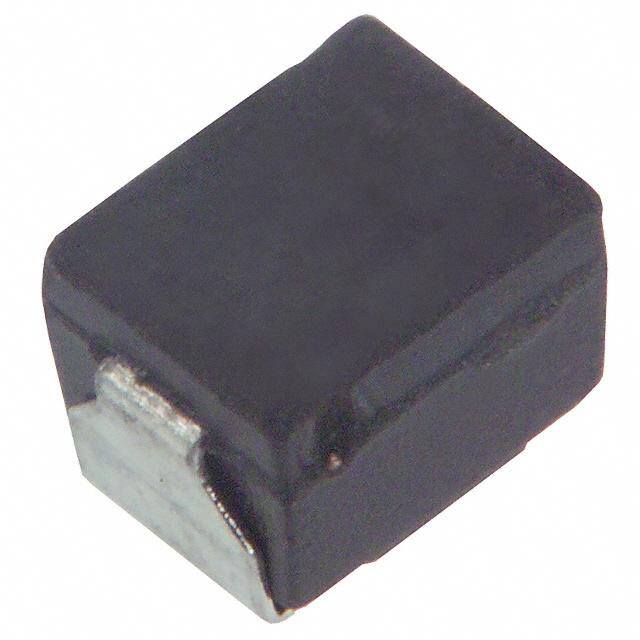
| 描述 | INDUCTOR 6.8UH 20% 1210 SMD固定电感器 1210 6.8uH 20% 200mA 250mohm Wirewound |
| 产品分类 | |
| 品牌 | Panasonic |
| 产品手册 | |
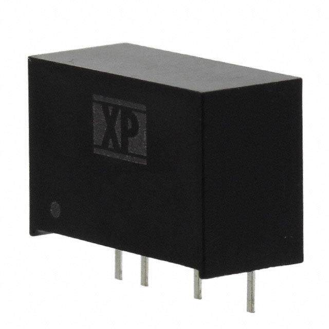
| 产品图片 |
|
| rohs | 符合RoHS无铅 / 符合限制有害物质指令(RoHS)规范要求 |
| 产品系列 | 固定电感器,Panasonic ELJ-EA6R8MFEA |
| 数据手册 | http://industrial.panasonic.com/www-cgi/jvcr13pz.cgi?E+PZ+3+AGA0016+ELJEA6R8MF+7+WW |
| 产品型号 | ELJ-EA6R8MF |
| PCN过时产品 | |
| Q最小值 | 7 |
| 不同频率时的Q值 | 7 @ 7.96MHz |
| 产品 | Inductors |
| 产品目录绘图 |
|
| 产品目录页面 | |
| 产品种类 | 固定电感器 |
| 供应商器件封装 | - |
| 其它名称 | PCD1422CT |
| 包装 | 剪切带 (CT) |
| 商标 | Panasonic |
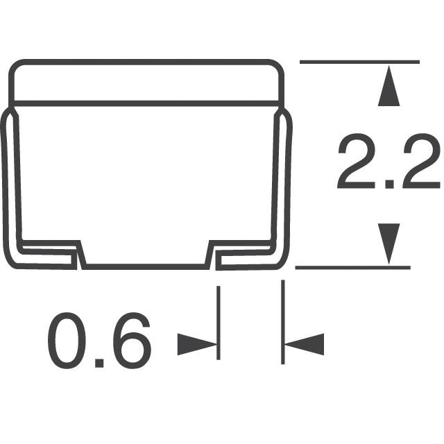
| 外壳宽度 | 2.5 mm |
| 外壳长度 | 3.2 mm |
| 外壳高度 | 2.2 mm |
| 大小/尺寸 | 0.126" 长x 0.098" 宽(3.20mm x 2.50mm) |
| 安装类型 | 表面贴装 |
| 容差 | 20 % |
| 封装 | Reel |
| 封装/外壳 | 1210(3225 公制) |
| 封装/箱体 | 1210 (3225 metric) |
| 屏蔽 | Unshielded |
| 工作温度 | -20°C ~ 85°C |
| 工作温度范围 | - 20 C to + 85 C |
| 工厂包装数量 | 2000 |
| 最大直流电流 | 200 mA |
| 最大直流电阻 | 190 mOhms |
| 材料-磁芯 | - |
| 标准包装 | 1 |
| 测试频率 | 7.96 MHz |
| 电感 | 6.8 uH |
| 电流-饱和值 | - |
| 端接类型 | SMD/SMT |
| 类型 | Chip Inductors |
| 系列 | ELJEA |
| 自谐振频率 | 36 MHz |
| 频率-测试 | 7.96MHz |
| 频率-自谐振 | 36MHz |
| 额定电流 | 200mA |
| 高度-安装(最大值) | 0.095" (2.40mm) |


- 商务部:美国ITC正式对集成电路等产品启动337调查
- 曝三星4nm工艺存在良率问题 高通将骁龙8 Gen1或转产台积电
- 太阳诱电将投资9.5亿元在常州建新厂生产MLCC 预计2023年完工
- 英特尔发布欧洲新工厂建设计划 深化IDM 2.0 战略
- 台积电先进制程称霸业界 有大客户加持明年业绩稳了
- 达到5530亿美元!SIA预计今年全球半导体销售额将创下新高
- 英特尔拟将自动驾驶子公司Mobileye上市 估值或超500亿美元
- 三星加码芯片和SET,合并消费电子和移动部门,撤换高东真等 CEO
- 三星电子宣布重大人事变动 还合并消费电子和移动部门
- 海关总署:前11个月进口集成电路产品价值2.52万亿元 增长14.8%


PDF Datasheet 数据手册内容提取
Fixed Inductors (Chip Inductors) 6. Low DC Resistance Type EA ■ Features ● Low DCR, suitable for power circuitry. ● Magnetic shield effect using ferrite mixed outer molding. ● Capable of being Re-fl ow or fl ow soldered. ● Good for mounting. ● RoHS compliant ■ Recommended Applications ● AV equipment, Wireless communication equipment and various types of general electronic equipment. ■ Explanation of Part Numbers 1 2 3 4 5 6 7 8 9 10 11 (cid:38) (cid:45) (cid:43) (cid:38) (cid:34) (cid:18) (cid:51) (cid:22) (cid:44) (cid:39) Packaging Design No. Product code Type Inductance Inductance tolerance F Taping Chip Inductors EA 3225 (1210) 3R3 3.3 μH K ±10 % Size : mm (inch) 470 47 μH M ±20 % 561 560 μH ■ Storage Conditions ● Package : Normal temperature (–5 to 35 °C), normal humidity (85 %RH max.), shall not be exposed to direct sunlight and harmful gases and care should be taken so as not to cause dew. ● Operating Temperature : –20 to +85 °C ■ Storage Period ● Solderability may be reduced due to the conditions of high temperature and high humidity which causes the oxidation of tin-plated terminals. Even if storage conditions are within specifi ed limits, solderability may be reduced with the passage of time. Therefore, please control the storage conditions and try to use the product within 6 months of receipt. ■Packaging Methods, Soldering Conditions and Safety Precautions Please see Data Files. Design and specifi cations are each subject to change without notice. Ask factory for the current technical specifi cations before purchase and/or use. Should a safety concern arise regarding this product, please be sure to contact us immediately. 02 Sep. 2012
Fixed Inductors (Chip Inductors) ■ EA Type 3225 (1210) ● ● Dimensions in mm (not to scale) Recommended Land Pattern in mm (not to scale) Marking 2.5±0.2 1.9±0.1 o 2.4 9 t 1. 3.2±0.3 1.6 to 2.0 4.0 to 4.6 2 0. ± 2 2. 0.6±0.2 ■ Standard Packing Quantity ● 2000 pcs./Reel ■ Standard Parts Inductance Q Part No. (μH) Tolerance Test Freq. min. Test Freq. (MSHRzF) m✽1in. (ΩR) D±C3 ✽02% D(mCA C) umrraexn.t (%) (MHz) (MHz) ELJ EA1R0MF 1.0 100 0.07 500 ELJ EA1R5MF 1.5 80 0.08 390 ELJ EA2R2MF 2.2 65 0.10 350 M : ±20 % 7.96 7 7.96 ELJ EA3R3MF 3.3 50 0.12 270 ELJ EA4R7MF 4.7 46 0.14 240 ELJ EA6R8MF 6.8 36 0.19 200 ELJ EA100KF 10 29 0.26 160 ELJ EA150KF 15 25 0.32 145 ELJ EA220KF 22 18 0.50 115 2.52 10 2.52 ELJ EA330KF 33 16 0.70 95 ELJ EA470KF 47 13 1.0 80 K : ±10 % ELJ EA680KF 68 10 1.5 60 ELJ EA101KF 100 8.0 2.4 50 ELJ EA151KF 150 7.0 3.1 45 0.796 20 0.796 ELJ EA221KF 220 5.0 5.5 35 ELJ EA331KF 330 4.0 7.1 30 ✽1 : Self Resonant Frequency ✽2 : DC Resistance Design and specifi cations are each subject to change without notice. Ask factory for the current technical specifi cations before purchase and/or use. Should a safety concern arise regarding this product, please be sure to contact us immediately. 02 Sep. 2012
Fixed Inductors (Chip Inductors) ■ Packaging Methods (Taping) ● Punched Carrier Tape Dimensions in mm (not to scale) ● Type □F t1 P0 fD0 A B W E F P1 E RF, QF, PF 0.71 1.21 8.0 1.75 3.5 2.0 FW Part AB P2 P0 0D0 t1 t2 t2 P1 P2 Tape running RF, QF, PF 2.0 4.0 01.5 m0a.7x. m1a.0x. direction ● Embossed Carrier Tape Dimensions in mm (not to scale) ● Type □E, Type ND, Type □C A B W E F P1 t1 fD0 RE, QE, PE 1.0 1.8 8.0 1.75 3.5 4.0 E ND 1.45 2.25 8.0 1.75 3.5 4.0 NC, FC, PC, LC, SC 2.40 2.90 8.0 1.75 3.5 4.0 A F W B P2 P0 0D0 0D1 t1 t2 RE, QE, PE 2.0 4.0 01.5 00.6 (0.27) 1.2 Ccohmipponent fD1 P1 P2 P0 Tdairpeec triounn ning NC, FC,N PCD, LC, SC 22..00 44..00 0011..55 0011..01 ((00..2255)) 11..5855 t2 t1 fD0 E ● Type □A A B W E F P1 A NA, FA, PA, LA, F W 2.80 3.60 8.0 1.75 3.5 4.0 SA, EA, DA B P2 P0 0D0 t1 t2 t2 Chip component P1 P2 P0 Tdairpeec triounn ning NA, FA, PA, LA, 2.0 4.0 01.5 (0.25) 2.40 SA, EA, DA ● Type □B t1 fD0 P2 P0 E A B W E F P1 A FB, PB 3.60 4.90 12.0 1.75 5.5 8.0 F W B P2 P0 0D0 t1 t2 FB, PB 2.0 4.0 01.5 (0.30) 3.50 t2 Chip component P1 Tape running direction ● Taping Reel Dimensions in mm (not to scale) Parts A B C D E W E Types C RF, QF, PF, RE, QE, PE, ND, B NC, FC, PC, LC, SC, 180 60 13 21 2 9 NA, FA, PA, LA, SA, EA, DA D W FB, PB 180 60 13 21 2 13 A ■ Standard Packing Quantity/Reel Quantity Quantity Types ✽ Under conditions of high temperature and humidity RF, QF, PF 10000 pcs. RE, QE, PE, ND 3000 pcs. deterioration of the taping and packaging may be NC, FC, PC, LC, SC 2000 pcs. accelerated. NA, FA, PA, LA, SA, EA, DA 2000 pcs. Please carefully control storage conditions and use the FB, PB 500 pcs. product within 6 months of receipt. Design and specifi cations are each subject to change without notice. Ask factory for the current technical specifi cations before purchase and/or use. Should a safety concern arise regarding this product, please be sure to contact us immediately. 03 Sep. 2012
Fixed Inductors (Chip Inductors) Soldering Conditions ■ Refl ow soldering conditions T3 C) e (° T2 ur at perT1 m e T t1 t2 0 Time ● Pb free solder recommended temperature profi le Preheat Soldering Peak Temperature Time of Type T1 [°C] t1 [s] T2 [°C] t2 [s] T3 T3 Limit Refl ow □F 150 to 180 60 to 120 230 °C 40 max. 250 °C, 10 s 260 °C, 10 s 2 times max. □E 150 to 180 60 to 120 230 °C 40 max. 250 °C, 10 s 260 °C, 10 s 2 times max. □D 150 to 180 60 to 120 230 °C 40 max. 245 °C, 10 s 250 °C, 10 s 2 times max. □C 150 to 180 60 to 120 230 °C 40 max. 245 °C, 10 s 250 °C, 10 s 2 times max. □A 150 to 180 60 to 120 230 °C 40 max. 245 °C, 10 s 250 °C, 10 s 2 times max. □B 150 to 180 60 to 120 230 °C 40 max. 245 °C, 10 s 250 °C, 10 s 2 times max. ■ Flow soldering conditions Preheat: 130 to 150 °C, 60 to 180 s, Soldering: 260 °C, 5 s max. ■ Notes ● Solderability may be reduced due to the conditions of high temperature and high humidity which causes the oxidation of tin-plated terminals. Even if storage conditions are within specified limits, solderability may be reduced with the passage of time. Therefore, please control the storage conditions and try to use the product within 6 months of receipt. ● In case the product has been stored for a period longer than 6 months, use the product only after confi rmation of its solderability. Design and specifi cations are each subject to change without notice. Ask factory for the current technical specifi cations before purchase and/or use. Should a safety concern arise regarding this product, please be sure to contact us immediately. 03 Sep. 2012
Fixed Inductors (Chip Inductors) Safety Precautions (Common precautions for Chip Inductors) • When using our products, no matter what sort of equipment they might be used for, be sure to make a written agreement on the specifications with us in advance. The design and specifications in this catalog are subject to change without prior notice. • Do not use the products beyond the specifi cations described in this catalog. • This catalog explains the quality and performance of the products as individual components. Bef ore use, check and evaluate their operations when installed in your products. • Install the following systems for a failsafe design to ensure safety if these products are to be used in equipm ent where a defect in these products may cause the loss of human life or other signifi cant damage, such as damage to vehicles (aut o mob ile, train, vessel), traffic lights, medical equipment, aerospace equipment, elec tric heating ap plia nc es, comb us tion/gas equipment, rotating equipment, and disaster/crime prevention equipm ent. ✽ Systems equipped with a protection circuit and a protection device ✽ Systems equipped with a redundant circuit or other system to prevent an unsafe status in the event of a single fault Precautions for use 1. Operation range and environments 1 These products are designed and manufactured for general and stan dard use in general elec tron ic equipment (e.g. AV equipment, home electric app lia nc es, office equipment, information and comm un ic a tion equipment) 2 These products are not intended for use in the following special conditions. Bef ore using the products, care full y check the effects on their quality and performance, and determine whether or not they can be used. • In liquid, such as water, oil, chemicals, or organic solvent • In direct sunlight, outdoors, or in dust • In salty air or air with a high concentration of corrosive gas, such as Cl2, H2S, NH3, SO2, or NO2 • In an environment where these products cause dew condensation 2. Handling 1 Do not bring magnets or magnetized materials close to the product. The infl uence of their magnetic fi eld can change the inductance value. 2 Do not apply strong mechanical shocks by either dropping or collision with other parts. Excessive schock can damage the part. 3. Land pattern design 1 Please refer to the recommended land pattern for each type shown on the datasheet. 2 Avoid placing the chip inductor on any metal pattern except the recommended land pattern because a drop of Q and mutual conductance may occur. 3 In case of fl ow soldering, venting of soldering fl ux gases should be made for high density assemblies to get a good solder connection. 4 In case of refl ow soldering, consider the layout because taller components close to chip inductor tend to block thermal conduction. 4. Mounting 1 In general, magnetic and electric characteristics of ferrite cores can be changed by applying excessively strong force. Placement force should not exceed 20 N. 2 Do not bend or twist the PWB after mounting the part. 5. Cleaning 1 Do not use acid or alkali agents. Some cleaning solvents may damage the part. Confi rm by testing the reliability in advance of mass production. 2 If Ultrasonic cleaning is used, please confi rm the reliability in advance. It is possible that combined resonance of component and PWB and cavitation can cause an abnormal vibration mode to exist causing damage. 6. Caution about applying excessive current The rated current is defi ned as the smaller value of either the current value when the inductance drops 10 % down from the initial point or the current value when the average temperature of coil inside rises 20 °C up from the initial point. Do not operate product over the specifi c max. current. <Package markings> Package markings include the product number, quantity, and country of origin. In principle, the country of origin should be indicated in English. Design and specifi cations are each subject to change without notice. Ask factory for the current technical specifi cations before purchase and/or use. Should a safety concern arise regarding this product, please be sure to contact us immediately. 01 Sep. 2012
Fixed Inductors (Chip Inductors) Chip Inductors □F, □E, □D, □C, □A, □B Type: □F □E □D □C □A □B (Size 1005) (Size 1608) (Size 2012) (Size 2520) (Size 3225) (Size 4532) Ceramic Core/Laser-Cut and wire wound type chip inductors for automatic and high-density mounting Wide variation product line-up correspond to various needs ■ Recommended Applications ● Cellular phones, wireless communication equipment (W-LAN, Bluetooth), various modules, HIC, TV, VTR, PC & peripherals, DVD, DSC, STB. ■ Inductors · Selection Guide Size : mm (inch) Non wound Wire wound Technology Case Size 1005 Size 1608 Size 2012 Size 2520 Size 3225 Size 4532 Usage (0402) (0603) (0805) (1008) (1210) (1812) ELJRF ELJRE ELJND ELJNC ELJNA High Freq. Use 1.0–100 nH 1.0–220 nH 10–1000 nH 10–820 nH 47–8200 nH ELJQF ELJQE High Freq. High-Q 1.0–39 nH 2.2–56 nH ELJFC ELJFA ELJFB General Use 0.22–100 µH 0.22–220 µH 0.22–1000 µH ELJPF ELJPE ELJPC/PC□3 ELJPA/PA□2 ELJPB ELJLC ELJLA High Power 2.2–10 nH 2.2–22 nH 1.0–33 µH 1.0–330 µH 10–220 µH ELJSC ELJSA Magnetically Shielded 27–100 µH 10–270 µH ELJEA Low DC Resistance 1.0–330 µH ELJDA/ELJFA Signal Processing Use (Low Distortion Type) 39–100 µH Design and specifi cations are each subject to change without notice. Ask factory for the current technical specifi cations before purchase and/or use. Should a safety concern arise regarding this product, please be sure to contact us immediately. 03 Sep. 2012