ICGOO在线商城 > 集成电路(IC) > 线性 - 放大器 - 仪表,运算放大器,缓冲器放大器 > EL5162ISZ
 Datasheet下载
- 型号: EL5162ISZ
- 制造商: Intersil
- 库位|库存: xxxx|xxxx
- 要求:
| 数量阶梯 | 香港交货 | 国内含税 |
| +xxxx | $xxxx | ¥xxxx |
查看当月历史价格
查看今年历史价格
EL5162ISZ产品简介:
ICGOO电子元器件商城为您提供EL5162ISZ由Intersil设计生产,在icgoo商城现货销售,并且可以通过原厂、代理商等渠道进行代购。 EL5162ISZ价格参考。IntersilEL5162ISZ封装/规格:线性 - 放大器 - 仪表,运算放大器,缓冲器放大器, 电流反馈 放大器 1 电路 8-SOIC。您可以下载EL5162ISZ参考资料、Datasheet数据手册功能说明书,资料中有EL5162ISZ 详细功能的应用电路图电压和使用方法及教程。
EL5162ISZ 是由 Renesas Electronics America Inc. 生产的高性能仪表放大器,属于线性放大器类别。该器件具有高精度、低噪声和高共模抑制比(CMRR)等特性,适用于多种精密测量和信号处理应用。

 应用场景

1. 医疗设备:
   - EL5162ISZ 可用于心电图(ECG)、脑电图(EEG)和其他生物电位测量设备中。其高共模抑制比能够有效消除干扰信号,确保采集到的生理信号准确无误。

2. 工业自动化:
   - 在传感器信号调理电路中,EL5162ISZ 可以放大来自压力、温度或位移传感器的微弱信号,同时保持高精度和稳定性。这使得它在工业控制系统、数据采集系统和自动化测试设备中非常有用。

3. 音频处理:
   - 该放大器可用于专业音频设备中的前置放大器,确保输入信号的高保真度。其低噪声特性使得音频信号在放大过程中不会引入额外的杂音,从而提升音质。

4. 科学仪器:
   - 在实验室环境中,EL5162ISZ 可用于各种精密测量仪器,如示波器、频谱分析仪等。它能够精确地放大微弱信号,帮助研究人员获得更准确的实验数据。

5. 汽车电子:
   - 在汽车传感器和控制系统中,EL5162ISZ 可用于放大来自各类传感器(如加速度计、陀螺仪等)的信号,确保车辆动态控制系统的稳定性和可靠性。

6. 消费电子产品:
   - 在高端音频设备、智能家居传感器等消费电子产品中,EL5162ISZ 的高精度和低噪声特性可以提升产品的性能和用户体验。

 总结
EL5162ISZ 凭借其卓越的性能和可靠性,广泛应用于医疗、工业、音频、科学仪器、汽车电子和消费电子等多个领域。它能够在复杂环境中提供稳定的信号放大和处理,是高精度测量和信号处理的理想选择。
| 参数 | 数值 |
| -3db带宽 | 500MHz |
| 产品目录 | 集成电路 (IC) |
| 描述 | IC OPAMP CFA 500MHZ 8SOIC |
| 产品分类 | Linear - Amplifiers - Instrumentation, OP Amps, Buffer Amps |
| 品牌 | Intersil |
| 数据手册 | |
| 产品图片 |
|
| 产品型号 | EL5162ISZ |
| PCN组件/产地 | |
| rohs | 无铅 / 符合限制有害物质指令(RoHS)规范要求 |
| 产品系列 | - |
| 产品目录页面 | |
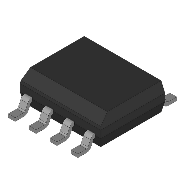
| 供应商器件封装 | 8-SOIC |
| 包装 | 管件 |
| 压摆率 | 4000 V/µs |
| 增益带宽积 | - |
| 安装类型 | 表面贴装 |
| 封装/外壳 | 8-SOIC(0.154",3.90mm 宽) |
| 工作温度 | -40°C ~ 85°C |
| 放大器类型 | 电流反馈 |
| 标准包装 | 97 |
| 电压-电源,单/双 (±) | 5 V ~ 12 V, ±2.5 V ~ 6 V |
| 电压-输入失调 | 1.5mV |
| 电流-电源 | 1.5mA |
| 电流-输入偏置 | 2µA |
| 电流-输出/通道 | 100mA |
| 电路数 | 1 |
| 输出类型 | - |


PDF Datasheet 数据手册内容提取
DATASHEET EL5162, EL5163, EL5262, EL5263, EL5362 FN7388 500MHz Low Power Current Feedback Amplifiers with Enable Rev 1.00 August 26, 2015 The EL5162, EL5163, EL5262, EL5263 and EL5362 are Features current feedback amplifiers with a bandwidth of 500MHz. This makes these amplifiers ideal for today’s high speed video and • 500MHz -3dB bandwidth monitor applications. • 4000V/µs slew rate (EL5162 and EL5163) With a supply current of just 1.5mA per amplifier and the • 1.5mA supply current per amplifier ability to run from a single supply voltage from 5V to 12V, • Single and dual supply operation, from 5V to 12V supply these amplifiers are also ideal for handheld, portable or span battery-powered equipment. • Fast enable/disable (EL5162, EL5262 and EL5362 only) The EL5162, EL5262 and EL5362 also incorporate an enable • Available in SOT-23 packages and disable function to reduce the supply current to 14µA typical per amplifier. Allowing the CE pin to float or applying a • Pb-free (RoHS compliant) low logic level enables the amplifier. • High speed, 1.4GHz product available (EL5166 and EL5167) The EL5162 is available in 6 Ld SOT-23 and 8 Ld SOIC • High speed, 4mA, 600MHz product available (EL5164, packages, the EL5163 in 5 Ld SOT-23 and SC-70 packages, EL5165 and EL5364) the EL5262 in the 10 Ld MSOP package, the EL5263 in 8 Ld Applications MSOP and SOIC packages, and the EL5362 in 16 Ld SOIC (0.150”) and QSOP packages. All operate over the industrial • Battery-powered equipment temperature range of -40°C to +85°C. • Handheld portable devices • Video amplifiers • Cable drivers • RGB amplifiers • Test equipment • Instrumentation • Current to voltage converters FN7388 Rev 1.00 Page 1 of 18 August 26, 2015
EL5162, EL5163, EL5262, EL5263, EL5362 Ordering Information PART NUMBER PART PACKAGE PKG. (Notes2, 3) MARKING (RoHS Compliant) DWG. # EL5162ISZ 5162ISZ 8 Ld SOIC (150mil) M8.15E EL5162ISZ-T7 (Note1) 5162ISZ 8 Ld SOIC (150mil) M8.15E EL5162ISZ-T13 (Note1) 5162ISZ 8 Ld SOIC (150mil) M8.15E EL5162ISZ-T7A 5162ISZ 8 Ld SOIC (150mil) M8.15E EL5162IWZ-T7 (Note1) (No longer available, recommended BAKA (Note4) 6 Ld SOT-23 P6.064A replacement: EL5163IWZ-T7) EL5162IWZ-T7A (Note1) (No longer available, recommended BAKA (Note4) 6 Ld SOT-23 P6.064A replacement: EL5163IWZ-T7A) EL5163IWZ-T7 (Note1) BALA (Note4) 5 Ld SOT-23 P5.064A EL5163IWZ-T7A (Note1) BALA (Note4) 5 Ld SOT-23 P5.064A EL5163ICZ-T7 (Note1) (No longer available, recommended BDA (Note4) 5 Ld SC-70 (1.25mm) P5.049 replacement: EL5163IWZ-T7) EL5163ICZ-T7A (Note1) (No longer available, recommended BDA (Note4) 5 Ld SC-70 (1.25mm) P5.049 replacement: EL5163IWZ-T7) EL5262IYZ BBTAA 10 Ld MSOP (3.0mm) M10.118A EL5262IYZ-T7 (Note1) BBTAA 10 Ld MSOP (3.0mm) M10.118A EL5262IYZ-T13 (Note1) BBTAA 10 Ld MSOP (3.0mm) M10.118A EL5263ISZ 5263ISZ 8 Ld SOIC (150mil) M8.15E EL5263ISZ-T7 (Note1) 5263ISZ 8 Ld SOIC (150mil) M8.15E EL5263ISZ-T13 (Note1) 5263ISZ 8 Ld SOIC (150mil) M8.15E EL5263IYZ BBBJA 8 Ld MSOP (3.0mm) M8.118A EL5263IYZ-T7 (Note1) BBBJA 8 Ld MSOP (3.0mm) M8.118A EL5263IYZ-T13 (Note1) BBBJA 8 Ld MSOP (3.0mm) M8.118A EL5362ISZ EL5362ISZ 16 Ld SOIC (150mil) MDP0027 EL5362ISZ-T7 (Note1) EL5362ISZ 16 Ld SOIC (150mil) MDP0027 EL5362ISZ-T13 (Note1) EL5362ISZ 16 Ld SOIC (150mil) MDP0027 EL5362IUZ 5362IUZ 16 Ld QSOP MDP0040 EL5362IUZ-T7 (Note1) 5362IUZ 16 Ld QSOP MDP0040 EL5362IUZ-T13 (Note1) 5362IUZ 16 Ld QSOP MDP0040 NOTES: 1. Please refer to TB347 for details on reel specifications. 2. These Intersil Pb-free plastic packaged products employ special Pb-free material sets, molding compounds/die attach materials, and 100% matte tin plate plus anneal (e3 termination finish, which is RoHS compliant and compatible with both SnPb and Pb-free soldering operations). Intersil Pb-free products are MSL classified at Pb-free peak reflow temperatures that meet or exceed the Pb-free requirements of IPC/JEDEC J STD-020. 3. For Moisture Sensitivity Level (MSL), please see product information page for EL5162, EL5163, EL5262, EL5263, EL5362. For more information on MSL, please see tech brief TB363. 4. The part marking is located on the bottom of the part. FN7388 Rev 1.00 Page 2 of 18 August 26, 2015
EL5162, EL5163, EL5262, EL5263, EL5362 Pin Configurations EL5162 EL5162 EL5163 (8 LD SOIC) (6 LD SOT-23) (5 LD SOT-23, SC-70) TOP VIEW TOP VIEW TOP VIEW NC 1 8 CE OUT 1 6 VS+ OUT 1 5 VS+ IN- 2 - 7 VS+ VS- 2 5 CE VS- 2 + - + + - IN+ 3 6 OUT IN+ 3 4 IN- IN+ 3 4 IN- VS- 4 5 NC EL5262 EL5263 EL5362 (10 LD MSOP) (8 LD SOIC, MSOP) (16 LD SOIC, QSOP) TOP VIEW TOP VIEW TOP VIEW OUT 1 10VS+ OUT1 1 8 VS+ INA+ 1 16INA- - IN- 2 9 OUT IN- 2 7 OUT2 CEA 2 15OUTA - - + + + IN+ 3 8 IN- IN+ 3 6 IN- VS- 3 14VS+ - - + + + VS- 4 77 IN+ VS- 4 5 IN+ CEB 4 13OUTB - CE 5 6 CE INB+ 5 12INB- NC 6 11 NC + CEC 7 10OUTC - INC+ 8 9 INC- FN7388 Rev 1.00 Page 3 of 18 August 26, 2015
EL5162, EL5163, EL5262, EL5263, EL5362 Absolute Maximum Ratings Thermal Information (TA = +25°C) Supply Voltage between VS+ and VS-. . . . . . . . . . . . . . . . . . . . . . . . . . 13.2V Maximum Storage Temperature Range . . . . . . . . . . . . . -65°C to +150°C Maximum Continuous Output Current. . . . . . . . . . . . . . . . . . . . . . . . . 50mA Ambient Operating Temperature Range. . . . . . . . . . . . . . -40°C to +85°C Maximum Slew Rate of VS+ to VS-. . . . . . . . . . . . . . . . . . . . . . . . . . . . 1V/µs Maximum Operating Junction Temperature. . . . . . . . . . . . . . . . . . +125°C Maximum Voltage between IN+ and IN-, disabled. . . . . . . . . . . . . . . ±1.5V Maximum Power Dissipation . . . . . . . . . . . . . . . . . . See Curves on page8 Current into IN+, IN-, CE. . . . . . . . . . . . . . . . . . . . . . . . . . . . . . . . . . . . . ±5mA Pb-free Reflow Profile . . . . . . . . . . . . . . . . . . . . . . . . . . . . . . . . . . see TB493 Pin Voltages. . . . . . . . . . . . . . . . . . . . . . . . . . . . . . (VS-) -0.5V to (VS+) +0.5V CAUTION: Do not operate at or near the maximum ratings listed for extended periods of time. Exposure to such conditions may adversely impact product reliability and result in failures not covered by warranty. Electrical Specifications VS+ = +5V, VS- = -5V, RF = 750Ω for AV = 1, RF = 400Ω for AV = 2, RL = 150Ω, CE = 0V, TA = +25°C unless otherwise specified. Boldface limits apply across the operating temperature range, -40°C to +85°C. MIN MAX PARAMETER DESCRIPTION TEST CONDITIONS (Note6) TYP (Note6) UNIT AC PERFORMANCE BW -3dB Bandwidth AV = +1, RL = 500ΩRF = 598Ω 500 MHz AV = +2, RL = 150ΩRF = 422Ω 233 MHz BW1 0.1dB Bandwidth 30 MHz SR Slew Rate VO = -2.5V to +2.5V, AV = +2, RL = 100Ω 2000 2500 4000 V/µs (EL5262, EL5263, EL5362) VO = -2.5V to +2.5V, AV = +2, RL = 100Ω 2800 4000 6000 V/µs (EL5162, EL5163) tS 0.1% Settling Time VOUT = -2.5V to +2.5V, AV = +1 25 ns eN Input Voltage Noise 3 nV/Hz iN- IN- Input Current Noise 10 pA/Hz iN+ IN+ Input Current Noise 6.5 pA/Hz dG Differential Gain Error (Note5) AV = +2 0.05 % dP Differential Phase Error (Note5) AV = +2 0.15 ° DC PERFORMANCE VOS Offset Voltage -5 1.5 +5 mV TCVOS Input Offset Voltage Temperature Measured from TMIN to TMAX 6 µV/°C Coefficient ROL Open Loop Transimpedance Gain 500 1000 kΩ INPUT CHARACTERISTICS CMIR Common Mode Input Range Guaranteed by CMRR test ±3 ±3.3 V CMRR Common Mode Rejection Ratio VIN = ±3V 50 62 75 dB -ICMR - Input Current Common Mode Rejection -1 0.22 +1 µA/V +IIN + Input Current -8 0.5 +8 µA -IIN - Input Current -10 2 +10 µA RIN Input Resistance 0.8 1.6 3 MΩ CIN Input Capacitance 1 pF FN7388 Rev 1.00 Page 4 of 18 August 26, 2015
EL5162, EL5163, EL5262, EL5263, EL5362 Electrical Specifications VS+ = +5V, VS- = -5V, RF = 750Ω for AV = 1, RF = 400Ω for AV = 2, RL = 150Ω, CE = 0V, TA = +25°C unless otherwise specified. Boldface limits apply across the operating temperature range, -40°C to +85°C. (Continued) MIN MAX PARAMETER DESCRIPTION TEST CONDITIONS (Note6) TYP (Note6) UNIT OUTPUT CHARACTERISTICS VO Output Voltage Swing RL = 150Ω to GND ±3.35 ±3.6 ±3.75 V RL = 1kΩ to GND ±3.75 ±3.9 ±4.15 V IOUT Output Current RL = 10Ω to GND 60 100 mA SUPPLY ISON Supply Current - Enabled, per Amplifier No load, VIN = 0V 1.3 1.5 2.0 mA ISOFF- Supply Current - Disabled, per Amplifier No load, VIN = 0V (EL5162, EL5262, EL5362 -25 -14 0 µA Only) ISOFF+ 0 10 +25 µA PSRR Power Supply Rejection Ratio DC, VS = ±4.75V to ±5.25V 65 76 dB -IPSR - Input Current Power Supply Rejection DC, VS = ±4.75V to ±5.25V -0.5 0.1 +0.5 µA/V ENABLE (EL5162, EL5262, EL5362 ONLY) tEN Enable Time 380 ns tDIS Disable Time 800 ns IIHCE CE Pin Input High Current CE = VS+ 1 5 25 µA IILCE CE Pin Input Low Current CE = (VS+) -5V -1 0 +1 µA VIHCE CE Input High Voltage for Power-down (VS+) - 1 V VILCE CE Input Low Voltage for Power-up (VS+) - 3 V NOTES: 5. Standard NTSC test, AC signal amplitude = 286mVP-P, f = 3.58MHz. 6. Compliance to datasheet limits is assured by one or more methods: production test, characterization and/or design. FN7388 Rev 1.00 Page 5 of 18 August 26, 2015
EL5162, EL5163, EL5262, EL5263, EL5362 Typical Performance Curves +4 +4 +3 VVSS+- == -+55VV +3 VVSS+-= = - 5+V5V B) +2 RL = 500Ω B) +2 RF = 375Ω N (d +1 RF = 598Ω N (d +1 GAI 0 GAI 0 ED -1 ED -1 Z Z LI -2 LI -2 A A M -3 M -3 R R O O N -4 N -4 -5 -5 -6 -6 100k 1M 10M 100M 1G 100k 1M 10M 100M 1G FREQUENCY (Hz) FREQUENCY (Hz) FIGURE 1. FREQUENCY RESPONSE FOR AV = +1 FIGURE 2. FREQUENCY RESPONSE FOR AV = +4.6 +2 +3 +1 +2 B) 0 B) +1 d d N ( -1 N ( 0 GAI -2 GAI -1 ED -3 ED -2 Z Z LI -4 LI -3 A A NORM ---567 VVARRVSSLF +- === == +13 +-57155050VVΩΩ NORM ---456 VVRRSSLF+- == == 14 -+525502VVΩΩ -8 -7 100k 1M 10M 100M 1G 100k 1M 10M 100M 1G FREQUENCY (Hz) FREQUENCY (Hz) FIGURE 3. FREQUENCY RESPONSE FOR AV = +10 FIGURE 4. FREQUENCY RESPONSE FOR AV = +2 +3 +5 +2 +4 AV = +1 RL = 150Ω dB) +1 B) +3 RF = 698Ω GAIN ( -01 AIN (d ++12 ±6V ED -2 D G 0 Z E ALI -3 LIZ -1 VS+, VS- = ±5V NORM --45 VVSS+- == -+55VV ORMA --23 ±±34VV RL = 150Ω N ±2.5V -6 RF = 422Ω -4 -7 -5 100k 1M 10M 100M 1G 100k 1M 10M 100M 500M FREQUENCY (Hz) FREQUENCY (Hz) FIGURE 5. FREQUENCY RESPONSE FOR AV = +4 FIGURE 6. FREQUENCY RESPONSE FOR VARIOUS ±VS FN7388 Rev 1.00 Page 6 of 18 August 26, 2015
EL5162, EL5163, EL5262, EL5263, EL5362 Typical Performance Curves (Continued) 100 VS+ = +5V VS+= +5V CE (Ω) 10 VAVS -= = + -25V VARVSL - == = +1 -5250VΩ 1V/DIV INPU1T. 0R2IS8nEs TIME N A D E P M T I 1 OUTPUT RISE 2V/DIV U TIME 2.218ns P T U O 0.1 10k 100k 1M 10M 100M 4ns/DIV FREQUENCY (Hz) FIGURE 7. CLOSED LOOP OUTPUT IMPEDANCE vs FREQUENCY FIGURE 8. EL5262 OUTPUT RISE TIME VS+ = +5V VS- = -5V CE INPUT FALL AV = +2 1V/DIV TIME 1.036ns RL = 150Ω OUTPUT FALL 2V/DIV TIME 2.21ns VOUT CE = 5V / DIV VOUT = 200mV / DIV M = 100ns 4ns/DIV 100ns/DIV FIGURE 9. EL5262 OUTPUT FALL TIME FIGURE 10. TURN ON TIME (EL5162, EL5262, EL5362) 0 VS+ = +5V -10 VS- = -5V -20 AV = +2 RL = 150Ω -30 CE B) -40 d CE = 5V / DIV RR ( -50 VOUT = 200mV / DIV PS -60 M = 100ns -70 -80 VOUT -90 -100 100 1k 10k 100k 1M 10M 100M 100ns/DIV FREQUENCY (Hz) FIGURE 11. TURN OFF TIME (EL5162, EL5262, EL5362) FIGURE 12. PSRR (VS+) vs FREQUENCY FN7388 Rev 1.00 Page 7 of 18 August 26, 2015
EL5162, EL5163, EL5262, EL5263, EL5362 Typical Performance Curves (Continued) JEDEC JESD51-7 HIGH EFFECTIVE THERMAL 0 CONDUCTIVITY TEST BOARD VS+ = +5V 1.4 -10 VS- = -5V --3200 ARVL == +1520Ω ON (W) 11..20 1.250W SJOA1 =6 +(08.01°5C0/”W) B) -40 TI PSRR (d --5600 DISSIPA 00..86 909mW SO8 -70 ER 0.4 JA = +110°C/W W -80 O P 0.2 -90 -100 0 100 1k 10k 100k 1M 10M 100M 0 25 50 7585 100 125 150 FREQUENCY (Hz) AMBIENT TEMPERATURE (°C) FIGURE 13. PSRR (VS-) vs FREQUENCY FIGURE 14. PACKAGE POWER DISSIPATION vs AMBIENT TEMPERATURE JEDEC JESD51-7 HIGH EFFECTIVE THERMAL JEDEC JESD51-7 HIGH EFFECTIVE THERMAL CONDUCTIVITY TEST BOARD CONDUCTIVITY TEST BOARD 1.4 0.50 435mW 0.45 W) 1.2 W) 0.40 ON ( 1.0 893mW ON ( 0.35 SOT23-5/6 PATI 0.8 QSOP16 PATI 0.30 JA = +230°C/W SI JA = +112°C/W SI 0.25 DIS 0.6 DIS 0.20 R R E 0.4 E 0.15 W W O O 0.10 P 0.2 P 0.05 0 0 0 25 50 7585 100 125 150 0 25 50 7585 100 125 150 AMBIENT TEMPERATURE (°C) AMBIENT TEMPERATURE (°C) FIGURE 15. PACKAGE POWER DISSIPATION vs AMBIENT FIGURE 16. PACKAGE POWER DISSIPATION vs AMBIENT TEMPERATURE TEMPERATURE JEDEC JESD51-7 HIGH EFFECTIVE THERMAL JEDEC JESD51-3 LOW EFFECTIVE THERMAL CONDUCTIVITY TEST BOARD CONDUCTIVITY TEST BOARD 1.0 1.0 870mW 0.9 0.9 W) 0.8 W) 0.8 909mW SO16 (0.15 0”) ON ( 0.7 MSOP8/10 ON ( 0.7 JA = +110°C/W ATI 0.6 JA = +115°C/W ATI 0.6 625mW P P SI 0.5 SI 0.5 S S DI 0.4 DI 0.4 SO8 ER 0.3 ER 0.3 JA = +160°C/W W W O 0.2 O 0.2 P P 0.1 0.1 0 0 0 25 50 75 85 100 125 0 25 50 7585 100 125 150 AMBIENT TEMPERATURE (°C) AMBIENT TEMPERATURE (°C) FIGURE 17. PACKAGE POWER DISSIPATION vs AMBIENT FIGURE 18. PACKAGE POWER DISSIPATION vs AMBIENT TEMPERATURE TEMPERATURE FN7388 Rev 1.00 Page 8 of 18 August 26, 2015
EL5162, EL5163, EL5262, EL5263, EL5362 Typical Performance Curves (Continued) JEDEC JESD51-3 LOW EFFECTIVE THERMAL JEDEC JESD51-3 LOW EFFECTIVE THERMAL CONDUCTIVITY TEST BOARD CONDUCTIVITY TEST BOARD 1.2 0.45 391mW 0.40 W) 1.0 W) N ( N ( 0.35 O 0.8 O 0.30 TI TI SOT23-5/6 SIPA 0.6 633mW QSOP16 SIPA 0.25 JA = +256°C/W DIS JA = +158°C/W DIS 0.20 R 0.4 R 0.15 E E W W 0.10 O O P 0.2 P 0.05 0 0 0 25 50 7585 100 125 150 0 25 50 7585 100 125 150 AMBIENT TEMPERATURE (°C) AMBIENT TEMPERATURE (°C) FIGURE 19. PACKAGE POWER DISSIPATION vs AMBIENT FIGURE 20. PACKAGE POWER DISSIPATION vs AMBIENT TEMPERATURE TEMPERATURE JEDEC JESD51-3 LOW EFFECTIVE THERMAL CONDUCTIVITY TEST BOARD 0.6 486mW W) 0.5 N ( O 0.4 MSOP8/10 ATI JA = +206°C/W P SI 0.3 S DI R 0.2 E W O P 0.1 0 0 25 50 75 85 100 125 AMBIENT TEMPERATURE (°C) FIGURE 21. PACKAGE POWER DISSIPATION vs AMBIENT TEMPERATURE FN7388 Rev 1.00 Page 9 of 18 August 26, 2015
EL5162, EL5163, EL5262, EL5263, EL5362 Revision History The revision history provided is for informational purposes only and is believed to be accurate, but not warranted. Please go to the web to make sure that you have the latest revision. DATE REVISION CHANGE August 26, 2015 FN7388.13 Updated the Ordering Information table on page2. April 6, 2015 FN7388.12 Added Note4 to the Ordering Information table on page2. Added Revision History and About Intersil. About Intersil Intersil Corporation is a leading provider of innovative power management and precision analog solutions. The company's products address some of the largest markets within the industrial and infrastructure, mobile computing and high-end consumer markets. For the most updated datasheet, application notes, related documentation and related parts, please see the respective product information page found at www.intersil.com. You may report errors or suggestions for improving this datasheet by visiting www.intersil.com/ask. Reliability reports are also available from our website at www.intersil.com/support © Copyright Intersil Americas LLC 2004-2015. All Rights Reserved. All trademarks and registered trademarks are the property of their respective owners. For additional products, see www.intersil.com/en/products.html Intersil products are manufactured, assembled and tested utilizing ISO9001 quality systems as noted in the quality certifications found at www.intersil.com/en/support/qualandreliability.html Intersil products are sold by description only. Intersil may modify the circuit design and/or specifications of products at any time without notice, provided that such modification does not, in Intersil's sole judgment, affect the form, fit or function of the product. Accordingly, the reader is cautioned to verify that datasheets are current before placing orders. Information furnished by Intersil is believed to be accurate and reliable. However, no responsibility is assumed by Intersil or its subsidiaries for its use; nor for any infringements of patents or other rights of third parties which may result from its use. No license is granted by implication or otherwise under any patent or patent rights of Intersil or its subsidiaries. For information regarding Intersil Corporation and its products, see www.intersil.com FN7388 Rev 1.00 Page 10 of 18 August 26, 2015
EL5162, EL5163, EL5262, EL5263, EL5362 Package Outline Drawing M8.15E 8 LEAD NARROW BODY SMALL OUTLINE PLASTIC PACKAGE Rev 0, 08/09 4 4.90 ± 0.10 A DETAIL "A" 0.22 ± 0.03 B 6.0 ± 0.20 3.90 ± 0.10 4 PIN NO.1 ID MARK 5 (0.35) x 45° 4° ± 4° 0.43 ± 0.076 1.27 0.25MC AB SIDE VIEW “B” TOP VIEW 1.75 MAX 1.45 ± 0.1 0.25 GAUGE PLANE C 0.175 ± 0.075 SEATING PLANE 0.10C SIDE VIEW “A 0.63 ±0.23 DETAIL "A" (1.27) (0.60) NOTES: (1.50) 1. Dimensions are in millimeters. Dimensions in ( ) for Reference Only. 2. Dimensioning and tolerancing conform to AMSE Y14.5m-1994. 3. Unless otherwise specified, tolerance : Decimal ± 0.05 (5.40) 4. Dimension does not include interlead flash or protrusions. Interlead flash or protrusions shall not exceed 0.25mm per side. 5. The pin #1 identifier may be either a mold or mark feature. 6. Reference to JEDEC MS-012. TYPICAL RECOMMENDED LAND PATTERN FN7388 Rev 1.00 Page 11 of 18 August 26, 2015
EL5162, EL5163, EL5262, EL5263, EL5362 Package Outline Drawing P6.064A 6 LEAD SMALL OUTLINE TRANSISTOR PLASTIC PACKAGE Rev 0, 2/10 1.90 0-3° 0.95 D 0.08-0.20 A 6 5 4 PIN 1 INDEX AREA 2.80 3 1.60 3 5 0.15 C D 2x (0.60) 1 2 3 0.20 C 2x SEE DETAIL X B 0.40 ±0.05 3 0.20 M C A-B D TOP VIEW END VIEW 10° TYP 5 0.15 C A-B (2 PLCS) 2.90 2x H 1.14 ±0.15 1.45 MAX C (0.25) GAUGE 0.10 C SEATING PLANE PLANE 0.05-0.15 SIDE VIEW DETAIL "X" 0.45±0.1 4 (0.60) (1.20) NOTES: (2.40) 1. Dimensions are in millimeters. Dimensions in ( ) for Reference Only. 2. Dimensioning and tolerancing conform to ASME Y14.5M-1994. 3. Dimension is exclusive of mold flash, protrusions or gate burrs. 4. Foot length is measured at reference to guage plane. 5. This dimension is measured at Datum “H”. 6. Package conforms to JEDEC MO-178AA. (0.95) (1.90) TYPICAL RECOMMENDED LAND PATTERN FN7388 Rev 1.00 Page 12 of 18 August 26, 2015
EL5162, EL5163, EL5262, EL5263, EL5362 Package Outline Drawing P5.064A 5 LEAD SMALL OUTLINE TRANSISTOR PLASTIC PACKAGE Rev 0, 2/10 1.90 0-3° D A 0.08-0.20 5 4 PIN 1 INDEX AREA 2.80 3 1.60 3 5 0.15 CD 2x 2 0.20 C (0.60) 2x 0.95 SEE DETAIL X B 0.40 ±0.05 3 END VIEW 0.20M C A-B D TOP VIEW 10° TYP (2 PLCS) 5 0.15 C A-B H 2.90 2x 1.45 MAX C 1.14 ±0.15 (0.25)GAUGE 0.10 C SEATING PLANE PLANE 0.45±0.1 4 SIDE VIEW 0.05-0.15 DETAIL "X" (0.60) (1.20) NOTES: 1. Dimensions are in millimeters. (2.40) Dimensions in ( ) for Reference Only. 2. Dimensioning and tolerancing conform to ASME Y14.5M-1994. 3. Dimension is exclusive of mold flash, protrusions or gate burrs. 4. Foot length is measured at reference to guage plane. 5. This dimension is measured at Datum “H”. 6. Package conforms to JEDEC MO-178AA. (0.95) (1.90) TYPICAL RECOMMENDED LAND PATTERN FN7388 Rev 1.00 Page 13 of 18 August 26, 2015
EL5162, EL5163, EL5262, EL5263, EL5362 Package Outline Drawing M10.118A (JEDEC MO-187-BA) 10 LEAD MINI SMALL OUTLINE PLASTIC PACKAGE (MSOP) Rev 0, 9/09 A 3.0 ± 0.1 10 0.25 CAB DETAIL "X" 1.10 Max SIDE VIEW 2 0.18 ± 0.05 3.0 ± 0.1 4.9 ± 0.15 PIN# 1 ID B 1 2 0.95 BSC 0.5 BSC TOP VIEW Gauge Plane H 0.86 ± 0.09 0.25 C SEATING PLANE 3°±3° 0.55 ± 0.15 0.10 ± 0.05 0.23 +0.07/ -0.08 0.10C 0.08 CAB DETAIL "X" SIDE VIEW 1 5.80 4.40 NOTES: 3.00 1. Dimensions are in millimeters. 2. Dimensioning and tolerancing conform to AMSE Y14.5m-1994. 0.50 3. Plastic or metal protrusions of 0.15mm max per side are not included. 4. Plastic interlead protrusions of 0.25mm max per side are not 0.30 included. 1.40 5. Dimensions “D” and “E1” are measured at Datum Plane “H”. TYPICAL RECOMMENDED LAND PATTERN 6. This replaces existing drawing # MDP0043 MSOP10L. FN7388 Rev 1.00 Page 14 of 18 August 26, 2015
EL5162, EL5163, EL5262, EL5263, EL5362 Package Outline Drawing M8.118A 8 LEAD MINI SMALL OUTLINE PLASTIC PACKAGE (MSOP) Rev 0, 9/09 A 3.0±0.1 8 0.25 CAB 4.9±0.15 DETAIL "X" 3.0±0.1 1.10 Max PIN# 1 ID B 0.18 ± 0.05 SIDE VIEW 2 1 2 0.65 BSC TOP VIEW 0.95 BSC 0.86±0.09 H GAUGE PLANE C 0.25 SEATING PLANE 0.33 +0.07/ -0.08 3°±3° 0.08 CAB 0.10 ± 0.05 0.10C 0.55 ± 0.15 DETAIL "X" SIDE VIEW 1 5.80 NOTES: 4.40 3.00 1. Dimensions are in millimeters. 2. Dimensioning and tolerancing conform to JEDEC MO-187-AA and AMSE Y14.5m-1994. 3. Plastic or metal protrusions of 0.15mm max per side are not 0.65 included. 0.40 4. Plastic interlead protrusions of 0.25mm max per side are not included. 1.40 5. Dimensions “D” and “E1” are measured at Datum Plane “H”. TYPICAL RECOMMENDED LAND PATTERN 6. This replaces existing drawing # MDP0043 MSOP 8L. FN7388 Rev 1.00 Page 15 of 18 August 26, 2015
EL5162, EL5163, EL5262, EL5263, EL5362 Small Outline Package Family (SO) A D h X 45° NN (N/2)+1 A PIN #1 I.D. MARK E E1 c SEE DETAIL “X” 1 (N/2) B L1 0.010M C A B e H C A2 GAUGE SEATING PLANE 0.010 PLANE A1 L 4° ±4° 0.004 C 0.010M C A B b DETAIL X MDP0027 SMALL OUTLINE PACKAGE FAMILY (SO) INCHES SO16 SO16 (0.300”) SO20 SO24 SO28 SYMBOL SO-8 SO-14 (0.150”) (SOL-16) (SOL-20) (SOL-24) (SOL-28) TOLERANCE NOTES A 0.068 0.068 0.068 0.104 0.104 0.104 0.104 MAX - A1 0.006 0.006 0.006 0.007 0.007 0.007 0.007 0.003 - A2 0.057 0.057 0.057 0.092 0.092 0.092 0.092 0.002 - b 0.017 0.017 0.017 0.017 0.017 0.017 0.017 0.003 - c 0.009 0.009 0.009 0.011 0.011 0.011 0.011 0.001 - D 0.193 0.341 0.390 0.406 0.504 0.606 0.704 0.004 1, 3 E 0.236 0.236 0.236 0.406 0.406 0.406 0.406 0.008 - E1 0.154 0.154 0.154 0.295 0.295 0.295 0.295 0.004 2, 3 e 0.050 0.050 0.050 0.050 0.050 0.050 0.050 Basic - L 0.025 0.025 0.025 0.030 0.030 0.030 0.030 0.009 - L1 0.041 0.041 0.041 0.056 0.056 0.056 0.056 Basic - h 0.013 0.013 0.013 0.020 0.020 0.020 0.020 Reference - N 8 14 16 16 20 24 28 Reference - Rev. M 2/07 NOTES: 1. Plastic or metal protrusions of 0.006” maximum per side are not included. 2. Plastic interlead protrusions of 0.010” maximum per side are not included. 3. Dimensions “D” and “E1” are measured at Datum Plane “H”. 4. Dimensioning and tolerancing per ASME Y14.5M-1994 FN7388 Rev 1.00 Page 16 of 18 August 26, 2015
EL5162, EL5163, EL5262, EL5263, EL5362 Small Outline Transistor Plastic Packages (SC70-5) P5.049 D VIEW C 5 LEAD SMALL OUTLINE TRANSISTOR PLASTIC PACKAGE e1 INCHES MILLIMETERS SYMBOL MIN MAX MIN MAX NOTES 5 4 A 0.031 0.043 0.80 1.10 - E CL A1 0.000 0.004 0.00 0.10 - 1 2 3 CL E1 A2 0.031 0.039 0.80 1.00 - b 0.006 0.012 0.15 0.30 - b1 0.006 0.010 0.15 0.25 e b c 0.003 0.009 0.08 0.22 6 CL c1 0.003 0.009 0.08 0.20 6 0.20 (0.008) M C C D 0.073 0.085 1.85 2.15 3 CL E 0.071 0.094 1.80 2.40 - E1 0.045 0.053 1.15 1.35 3 A A2 A1 SPELAATNINEG e 0.0256 Ref 0.65 Ref - e1 0.0512 Ref 1.30 Ref - -C- L 0.010 0.018 0.26 0.46 4 L1 0.017 Ref. 0.420 Ref. - 0.10 (0.004) C L2 0.006 BSC 0.15 BSC 0o 8o 0o 8o - b WITH N 5 5 5 PLATING b1 R 0.004 - 0.10 - R1 0.004 0.010 0.15 0.25 c c1 Rev. 3 7/07 NOTES: BASE METAL 1. Dimensioning and tolerances per ASME Y14.5M-1994. 2. Package conforms to EIAJ SC70 and JEDEC MO-203AA. 4X 1 3. Dimensions D and E1 are exclusive of mold flash, protrusions, or gate burrs. R1 4. Footlength L measured at reference to gauge plane. 5. “N” is the number of terminal positions. R 6. These Dimensions apply to the flat section of the lead between GAUGE PLANE 0.08mm and 0.15mm from the lead tip. SEATING 7. Controlling dimension: MILLIMETER. Converted inch dimen- L PLANE sions are for reference only. C L1 L2 4X 1 VIEW C 0.4mm 0.75mm 2.1mm 0.65mm TYPICAL RECOMMENDED LAND PATTERN FN7388 Rev 1.00 Page 17 of 18 August 26, 2015
EL5162, EL5163, EL5262, EL5263, EL5362 Quarter Size Outline Plastic Packages Family (QSOP) MDP0040 A D QUARTER SIZE OUTLINE PLASTIC PACKAGES FAMILY N (N/2)+1 INCHES SYMBOL QSOP16 QSOP24 QSOP28 TOLERANCE NOTES A 0.068 0.068 0.068 Max. - PIN #1 I.D. MARK E E1 A1 0.006 0.006 0.006 ±0.002 - A2 0.056 0.056 0.056 ±0.004 - b 0.010 0.010 0.010 ±0.002 - 1 (N/2) c 0.008 0.008 0.008 ±0.001 - B D 0.193 0.341 0.390 ±0.004 1, 3 0.010 CAB E 0.236 0.236 0.236 ±0.008 - e E1 0.154 0.154 0.154 ±0.004 2, 3 H e 0.025 0.025 0.025 Basic - C SEATING L 0.025 0.025 0.025 ±0.009 - PLANE L1 0.041 0.041 0.041 Basic - 0.004 C 0.007 CAB b N 16 24 28 Reference - Rev. F 2/07 L1 NOTES: 1. Plastic or metal protrusions of 0.006” maximum per side are not in- A cluded. 2. Plastic interlead protrusions of 0.010” maximum per side are not c included. SEE DETAIL "X" 3. Dimensions “D” and “E1” are measured at Datum Plane “H”. 4. Dimensioning and tolerancing per ASME Y14.5M-1994. 0.010 A2 GAUGE PLANE L A1 4°±4° DETAIL X FN7388 Rev 1.00 Page 18 of 18 August 26, 2015