ICGOO在线商城 > 晶体,振荡器,谐振器 > 振荡器 > DV75D-010.0M

 Datasheet下载
- 型号: DV75D-010.0M
- 制造商: Connor-Winfield
- 库位|库存: xxxx|xxxx
- 要求:
| 数量阶梯 | 香港交货 | 国内含税 |
| +xxxx | $xxxx | ¥xxxx |
查看当月历史价格
查看今年历史价格
DV75D-010.0M产品简介:
ICGOO电子元器件商城为您提供DV75D-010.0M由Connor-Winfield设计生产,在icgoo商城现货销售,并且可以通过原厂、代理商等渠道进行代购。 DV75D-010.0M价格参考。Connor-WinfieldDV75D-010.0M封装/规格:振荡器, 振荡器 10MHz LVCMOS TCXO 3.3V 4-SMD,无引线。您可以下载DV75D-010.0M参考资料、Datasheet数据手册功能说明书,资料中有DV75D-010.0M 详细功能的应用电路图电压和使用方法及教程。
Connor-Winfield的DV75D-010.0M是一款振荡器,主要用于需要高稳定性和精确频率控制的电子设备中。该型号属于电压控制晶体振荡器(VCXO),常应用于通信设备、测试仪器、工业控制系统以及精密计时装置中。其主要作用是在电路中提供稳定的参考频率信号,确保系统运行的稳定性与准确性。由于其良好的温度稳定性和低相位噪声特性,DV75D-010.0M也适用于对频率精度要求较高的科研和高端电子产品中。
| 参数 | 数值 |
| 产品目录 | 晶体和振荡器 |
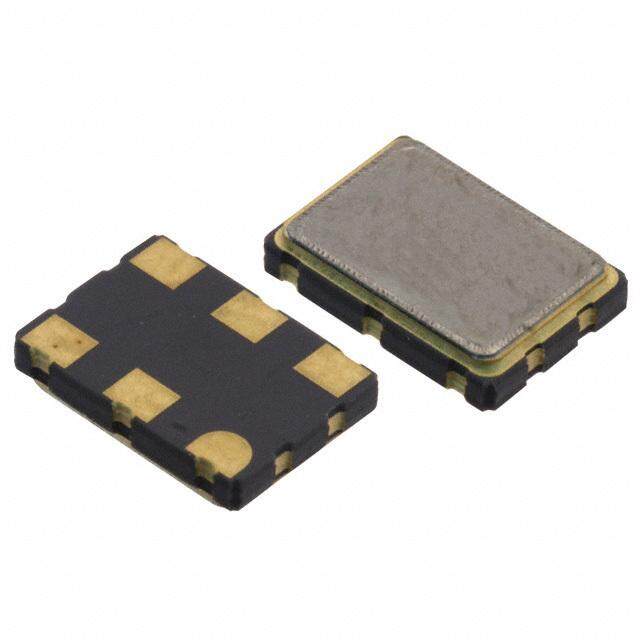
| 描述 | OSC TCXO 10.000MHZ LVCMOS SMD |
| 产品分类 | |
| 品牌 | Connor-Winfield |
| 数据手册 | |
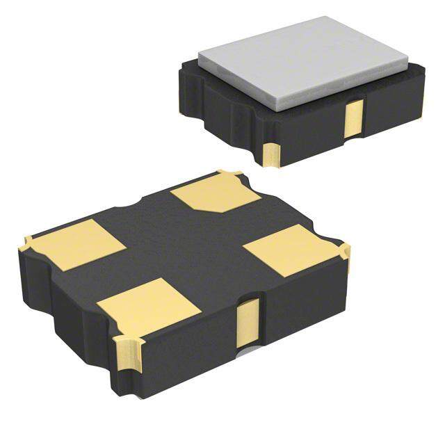
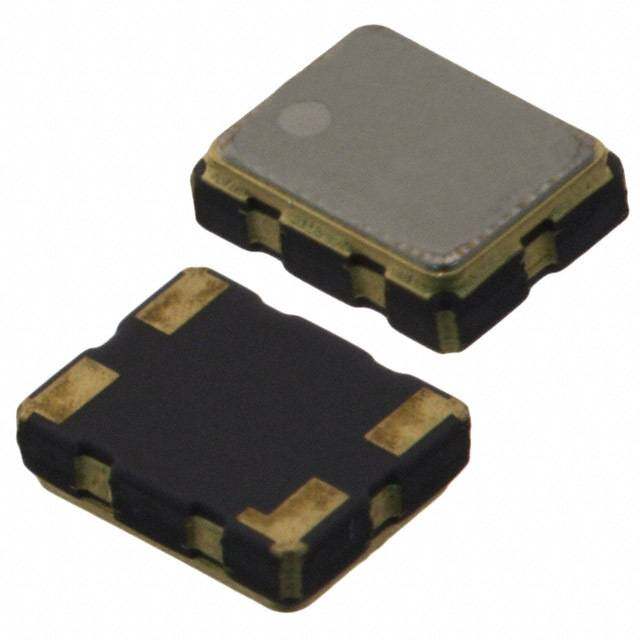
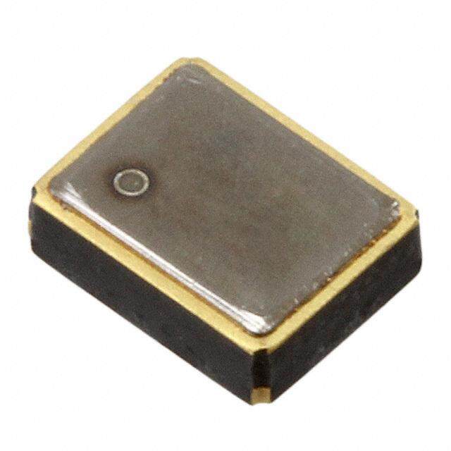
| 产品图片 |
|
| 产品型号 | DV75D-010.0M |
| rohs | 无铅 / 符合限制有害物质指令(RoHS)规范要求 |
| 产品系列 | DV75D |
| 其它名称 | CW743TR |
| 功能 | - |
| 包装 | 带卷 (TR) |
| 大小/尺寸 | 0.276" 长 x 0.197" 宽(7.00mm x 5.00mm) |
| 安装类型 | 表面贴装 |
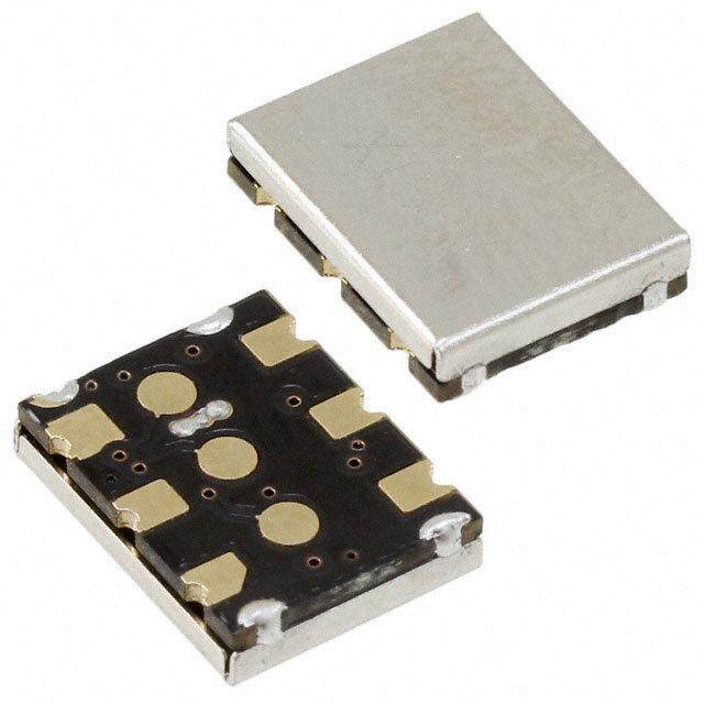
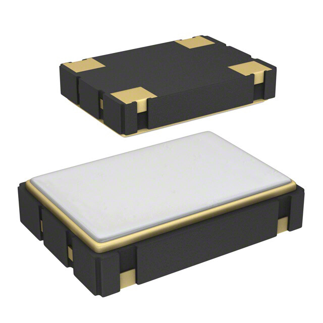
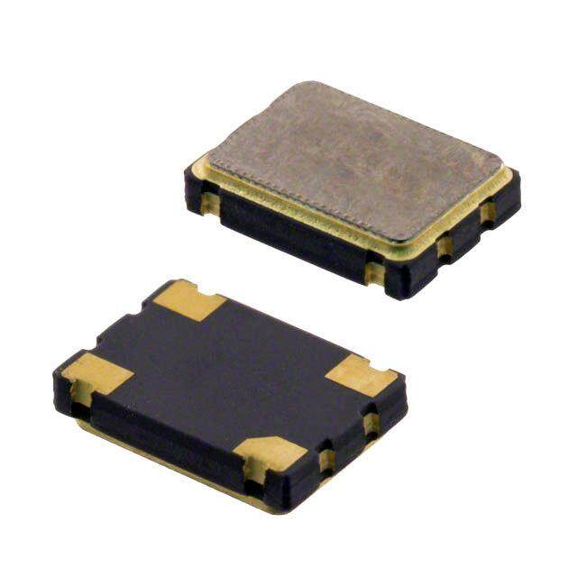
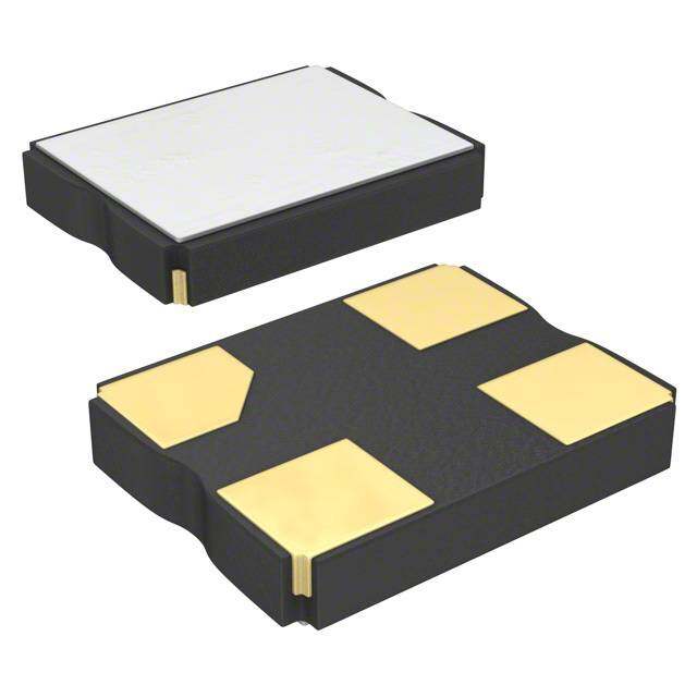
| 封装/外壳 | 4-SMD,无引线(DFN,LCC) |
| 工作温度 | -40°C ~ 85°C |
| 标准包装 | 250 |
| 特色产品 | http://www.digikey.cn/product-highlights/zh/dv75c-and-dv75d-series-tcxos/50334 |
| 电压-电源 | 3.3V |
| 电流-电源(最大值) | 6mA |
| 电流-电源(禁用)(最大值) | - |
| 等级 | - |
| 类型 | TCXO |
| 输出 | LVCMOS |
| 频率 | 10MHz |
| 频率稳定度 | ±1ppm |
| 高度 | 0.079"(2.00mm) |


- 商务部:美国ITC正式对集成电路等产品启动337调查
- 曝三星4nm工艺存在良率问题 高通将骁龙8 Gen1或转产台积电
- 太阳诱电将投资9.5亿元在常州建新厂生产MLCC 预计2023年完工
- 英特尔发布欧洲新工厂建设计划 深化IDM 2.0 战略
- 台积电先进制程称霸业界 有大客户加持明年业绩稳了
- 达到5530亿美元!SIA预计今年全球半导体销售额将创下新高
- 英特尔拟将自动驾驶子公司Mobileye上市 估值或超500亿美元
- 三星加码芯片和SET,合并消费电子和移动部门,撤换高东真等 CEO
- 三星电子宣布重大人事变动 还合并消费电子和移动部门
- 海关总署:前11个月进口集成电路产品价值2.52万亿元 增长14.8%


PDF Datasheet 数据手册内容提取
Available at Digi-Key www.digikey.com 5x7mm Precision TCXO Model DV75D Description: Features: The Connor-Winfield’s DV75D is a 5x7mm • TCXO 2111 Comprehensive Drive Surface Mount Temperature Compensated • 3.3 Vdc Operation Aurora, Illinois 60505 Crystal Controlled Oscillator (TCXO) with DV207.50DM1H2Z02 • LVCMOS Output LVCMOS output. Through the use of Analog • Frequency Stability: ± 1.0 ppm Phone: 630-851-4722 Temperature Compensation, the DV75D • Temperature Range: -40 to 85°C is capable of holding sub 1-ppm stabilities Fax: 630-851-5040 • Low Jitter <1ps RMS over the -40 to 85°C temperature range. • 5x7mm Surface Mount Package www.conwin.com Applications: • Tape and Reel Packaging • RoHS Compliant / Pb Free GR-253-CORE (SMC) ITU-T-G.813 Option 1 and 2 (SEC) Absolute Maximum Ratings Parameter Minimum Nominal Maximum Units Notes Storage Temperature -55 - 85 °C Supply Voltage (Vcc) -0.5 - 6.0 Vdc Input Voltage -0.5 - Vcc+0.5 Vdc Operating Specifications Parameter Minimum Nominal Maximum Units Notes Nominal Frequency (Fo) - 10.0, 12.8 or 20.0 - MHz Frequency Calibration @ 25 °C -1.0 - 1.0 ppm 1 Frequency Stability vs. Temperature -1.0 - 1.0 ppm 2 Frequency vs. Load Stability -0.05 - 0.05 ppm ±5% Frequency vs. Voltage Stability -0.05 - 0.05 ppm ±5% Static Temperature Hysteresis - - 0.4 ppm 3 Aging -1.0 - 1.0 ppm/year Operating Temperature Range: -40 - 85 °C Supply Voltage (Vcc) 3.135 3.3 3.465 Vdc ±5% Supply Current (Icc) - 2.1 6 mA Period Jitter - 3 5 ps rms Integrated Phase Jitter - 0.3 1.0 ps rms 4 Typical Phase Noise Fo = 20.0 MHz SSB Phase Noise at 10Hz offset - -90 - dBc/Hz SSB Phase Noise at 100Hz offset - -120 - dBc/Hz SSB Phase Noise at 1KHz offset - -140 - dBc/Hz SSB Phase Noise at 10KHz offset - -150 - dBc/Hz SSB Phase Noise at 100KHz offset - -150 - dBc/Hz Start-up Time - - 10 ms LVCMOS Output Characteristics Parameter Minimum Nominal Maximum Units Notes Load - 15 - pF 5 Voltage (High) (Voh) 90%Vcc - - Vdc (Low) (Vol) - - 10%Vcc Vdc Duty Cycle at 50% of Vcc 45 50 55 % Rise / Fall Time 10% to 90% - 4 8 ns Package Characteristics Package Hermetically sealed crystal mounted on a ceramic package Environmental Characteristics Vibration Vibration per Mil Std 883E Method 2007.3 Test Condition A Shock Mechanical Shock per Mil Std 883E Method 2002.4 Test Condition B. Soldering Process RoHS compliant lead free. See soldering profile on page 2. Ordering Information DV75D-010.0M, DV75D-012.8M or DV75D-020.0M Bulletin Tx356 Notes: Page 1 of 2 1. Initial calibration @ 25°C. Specifications at time of shipment after 48 hours of operation. 2. Frequency stability vs. change in temperature. [±(Fmax - Fmin)/(2*Fo)]. Revision 04 3. Frequency change after reciprocal temperature ramped over the operating range. Frequency measured before and after at 25°C. Date 11 June 2019 4. BW = 12 KHz to Fo/2 MHz. 5. For best performance it is recommended that the circuit connected to this output should have an equivalent input capacitance of 15pF.
2111 Comprehensive Drive Aurora, Illinois 60505 Phone: 630-851-4722 Fax: 630-851-5040 www.conwin.com Package Layout Suggested Pad Layout Pad Connections 1: N/C 0.276±0.006 0.095Max. 0.071 (7.0mm) (2.4mm) (1.8mm) 2: Ground (TopView) 4Places 3: Output (Fo) 4 3 4: Supply Voltage (Vcc) 0.197 DV75D1923 ±0.006 12.8MHZ (5.0mm) 0.165 0.047 Pad1 (4.2mm) (TopView) (1.2mm) 4Places Keep Output Waveform 1 2 Out * 0.034 (BottomView) D±±..i00m02e5n((s..15io20n78ammlTmmo))lerance: 1 (50.7.2m24m) 2 Area (0.90mm) (4Places) 4 3 0.055 * Do not route any traces in the keep out area. It is (1.40mm) recommended the next layer under the keep out area (4Places) is to be ground plane. Design Recommendations 1V/Div Vaccla,rsgheouclodphpaevre 0.010”(0.254mm) areaforreduced Recommended Vcc 50Ohmtrace Coninndeuccttaan0c.e0.1uF incdleuacrtaannccee <1”bydesign bypasscapacitor forinternal <fr0o.m1”(t2h.e54pmadm.) 4 3 copperflood. Buffer 9 5 Ground 10 4 Test Circuit 1 2 shGouroldunhda,ve TopView Ground TopView alargecopper areaforreduced inductance. Vcc 50OhmTrace Supply OSC Without Output Voltage Vias Buffer TOPLAYER 0.1uF 10nF 4 3 Output GROUNDLAYER ....... Bypass Bypass 1 2 15pF BOTTOMLAYER Attention: To achieve optimal frequency stability, and in some cases to meet the specification stated on this data N/C sheet, it is required that the circuit connected to this TCXO output must have the equivalent input capacitance that is specified by the nominal load capacitance. Deviations from the nominal load capacitance will have a graduated effect on the stability of approximately 20 ppb per pF load difference. Solder Profile Temperature Tape and Reel Dimensions 260°C 260°C 220°C 180°C 150°C 120°C 0 10s Upto120s Typical 60to90s Typical MeetsIPC/JEDECJ-STD-020C Revision History Revision Date Note 00 01/11/12 New issue 01 11/26/12 Removed tri-state information from features and description. Bulletin Tx356 02 04/15/13 Added "Applications. Page 2 of 2 03 12/03/13 Removed TR from Ordering Information. Revision 04 04 06/11/19 Updated stability, supply current, phase noise and height specifications. Date 11 June 2019 Specifications subject to change without notification. See Connor-Winfield's website for latest revision. © Copyright 2019 The Connor-Winfield Corporation Not intended for life support applications.