 Datasheet下载
- 型号: DT1240-04LP-7
- 制造商: Diodes Inc.
- 库位|库存: xxxx|xxxx
- 要求:
| 数量阶梯 | 香港交货 | 国内含税 |
| +xxxx | $xxxx | ¥xxxx |
查看当月历史价格
查看今年历史价格
DT1240-04LP-7产品简介:
ICGOO电子元器件商城为您提供DT1240-04LP-7由Diodes Inc.设计生产,在icgoo商城现货销售,并且可以通过原厂、代理商等渠道进行代购。 DT1240-04LP-7价格参考。Diodes Inc.DT1240-04LP-7封装/规格:TVS - 二极管, 。您可以下载DT1240-04LP-7参考资料、Datasheet数据手册功能说明书,资料中有DT1240-04LP-7 详细功能的应用电路图电压和使用方法及教程。
DT1240-04LP-7 是由 Diodes Incorporated 生产的一款 TVS(瞬态电压抑制)二极管,主要用于保护电子设备免受过电压事件的影响,例如静电放电 (ESD)、电感负载开关和雷击浪涌等。以下是该型号的应用场景:

1. 消费类电子产品:
   DT1240-04LP-7 可用于智能手机、平板电脑、笔记本电脑和其他便携式设备中,保护 USB 接口、HDMI 接口、音频接口以及数据传输线路免受 ESD 和其他瞬态电压的损害。

2. 通信设备:
   在路由器、调制解调器、网络交换机等通信设备中,这款 TVS 二极管可用于保护信号线路和电源线路,防止因雷击或电气干扰导致的损坏。

3. 工业自动化:
   工业控制设备、传感器和 PLC(可编程逻辑控制器)中的信号线和电源线需要可靠的保护。DT1240-04LP-7 可以有效抑制由于开关操作或外部干扰引起的电压尖峰。

4. 汽车电子系统:
   汽车内的电子控制单元 (ECU)、信息娱乐系统、导航系统和车载充电器可能面临复杂的电气环境。此 TVS 二极管可以保护这些系统免受电池反接、负载突降和感应尖峰的影响。

5. 医疗设备:
   医疗仪器如监护仪、超声波设备和便携式诊断工具对可靠性和安全性要求极高。DT1240-04LP-7 能够保护敏感电路,确保设备在各种环境下稳定运行。

6. 家用电器:
   在洗衣机、空调、冰箱等家电中,TVS 二极管可以保护微控制器和传感器免受电源波动和电磁干扰的影响,延长设备寿命。

总结来说,DT1240-04LP-7 的应用场景广泛覆盖了需要高可靠性保护的各种电子设备和系统,尤其适用于需要应对瞬态电压威胁的场合。
| 参数 | 数值 |
| 产品目录 | |
| 描述 | TVS DIODE 5.5VWM 11VC DFN |
| 产品分类 | |
| 品牌 | Diodes Incorporated |
| 数据手册 | |
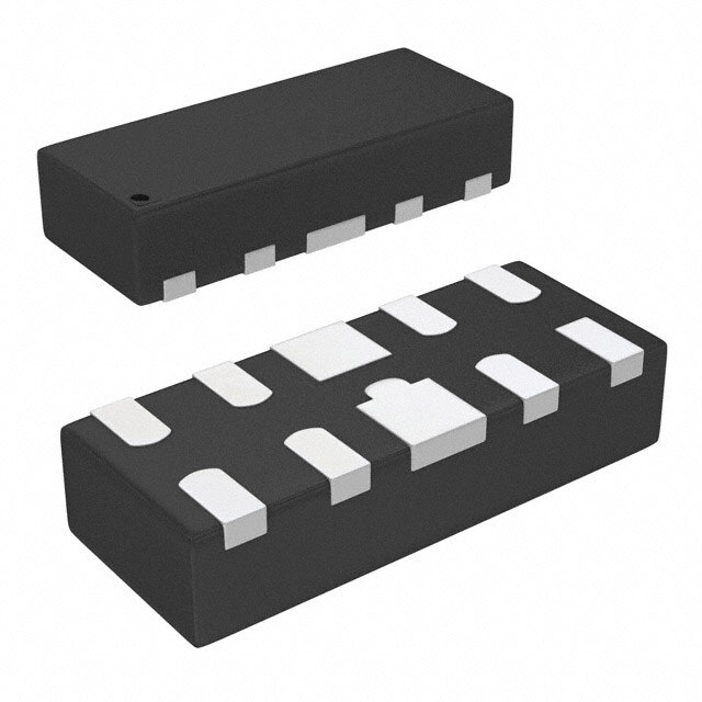
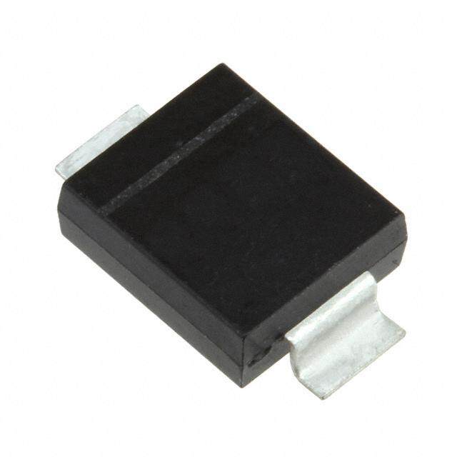
| 产品图片 |
|
| 产品型号 | DT1240-04LP-7 |
| rohs | 无铅 / 符合限制有害物质指令(RoHS)规范要求 |
| RoHS指令信息 | http://diodes.com/download/4349 |
| 产品系列 | - |
| 不同频率时的电容 | - |
| 供应商器件封装 | 10-DFN2510 (2.5x1) |
| 其它名称 | DT1240-04LP-7DIDKR |
| 功率-峰值脉冲 | 60W |
| 包装 | Digi-Reel® |
| 单向通道 | - |
| 双向通道 | 4 |
| 安装类型 | 表面贴装 |
| 封装/外壳 | 10-UFDFN |
| 工作温度 | -55°C ~ 85°C (TA) |
| 应用 | 以太网, HDMI |
| 标准包装 | 1 |
| 电压-击穿(最小值) | 6V |
| 电压-反向关态(典型值) | 5.5V(最小值) |
| 电压-箝位(最大值)@Ipp | 11V |
| 电流-峰值脉冲(10/1000µs) | 5.5A (8/20µs) |
| 电源线路保护 | 是 |
| 类型 | 转向装置(轨至轨) |


- 商务部:美国ITC正式对集成电路等产品启动337调查
- 曝三星4nm工艺存在良率问题 高通将骁龙8 Gen1或转产台积电
- 太阳诱电将投资9.5亿元在常州建新厂生产MLCC 预计2023年完工
- 英特尔发布欧洲新工厂建设计划 深化IDM 2.0 战略
- 台积电先进制程称霸业界 有大客户加持明年业绩稳了
- 达到5530亿美元!SIA预计今年全球半导体销售额将创下新高
- 英特尔拟将自动驾驶子公司Mobileye上市 估值或超500亿美元
- 三星加码芯片和SET,合并消费电子和移动部门,撤换高东真等 CEO
- 三星电子宣布重大人事变动 还合并消费电子和移动部门
- 海关总署:前11个月进口集成电路产品价值2.52万亿元 增长14.8%


PDF Datasheet 数据手册内容提取
DT1240-04LP 4 CHANNELS LOW CAPACITANCE TVS DIODE ARRAY Features & Applications Mechan ical Data Clamping Voltage: 9V at 10A 100ns, TLP Case: U-DFN2510-10 9.4V at 5.5A 8μs/20μs Case Material: Molded Plastic, “Green” Molding Compound. IEC 61000-4-2 (ESD): Air — ±16kV, Contact — ±14kV UL Flammability Classification Rating 94V-0 IEC 61000-4-4 (EFT): Level 4 Moisture Sensitivity: Level 1 per J-STD-020 N IEC 61000-4-5 (Lightning): ±5.5A (8/20µs) Terminals: NiPdAu over Copper Leadframe (Lead Free Plating). O O 4 Channels of ESD Protection Solderable per MIL-STD-202, Method 208 e4 Low Channel Input Capacitance of 0.55pF Typical II Weight: 0.038 grams (Approximate) TT TLP Dynamic Resistance: 0.25Ω AA Typically Used for High Speed Ports such as USB 2.0, USB 3.0 ® MM DVI™, HDMI2.0, Ethernet Port, IEEE, MDDI, PCI Express , RR SATA/ eSATA OO Totally Lead-Free & Fully RoHS Compliant (Notes 1 & 2) Halogen, Antimony and Beryllium Free. “Green” Device FF NN (Note 3) An Automotive-Compliant Part is Available Under Separate II Datasheet (DT1240-04LPQ) ED U-DFN2510-10 and U-DFN2510-10 (Type CJ) CE NC AN P i n # Description 10 9 8 7 6 VA 1 , 2 , 4 , 5 I / O Pin 1 Pin 2 Pin 4 Pin 5 DV 6, 7, 9, 10 No Connection AD 3, 8 Vss 1 2 3 4 5 A 3,8 Pin Description (Top View) Device Schematic Ordering Information (Note 4) Part Number Compliance Marking Reel Size (inches) Tape Width (mm) Quantity per Reel DT1240-04LP-7 Standard BC7 7 8 3,000/Tape & Reel Notes: 1. No purposely added lead. Fully EU Directive 2002/95/EC (RoHS), 2011/65/EU (RoHS 2) & 2015/863/EU (RoHS 3) compliant. 2. See https://www.diodes.com/quality/lead-free/ for more information about Diodes Incorporated’s definitions of Halogen- and Antimony-free, "Green" and Lead-free. 3. Halogen- and Antimony-free "Green” products are defined as those which contain <900ppm bromine, <900ppm chlorine (<1500ppm total Br + Cl) and <1000ppm antimony compounds. 4. For packaging details, go to our website at https://www.diodes.com/design/support/packaging/diodes-packaging/. Marking Information BC7 = Product Type Marking Code BC7 = Product Type Marking Code YWX = Date Code Marking YM = Date Code Marking Y = Year (ex: 9 = 2019) BTCF27 YM Y = Year (ex: G = 2019) BTCF72 YWYMX W = Week M = Month (ex: 9 = September) (ex: a=Week 27; z Represents Week 52 and 53) X = Internal Code (ex: U=Monday) Date Code Key for YM Year 2019 2020 2021 2022 2023 2024 Code G H I J K L Month Jan Feb Mar Apr May Jun Jul Aug Sep Oct Nov Dec Code 1 2 3 4 5 6 7 8 9 O N D Date Code Key for YWX Year 2019 2020 2021 2022 2023 2024 2025 Code 9 0 1 2 3 4 5 Week 1-26 27-52 53 Code A-Z a-z z Internal Code Sun Mon Tue Wed Thu Fri Sat Code T U V W X Y Z PCI Express is a trademark or registered trademark of PCI-SIG. DT1240-04LP 1 of 7 May 2019 Document number: DS36312 Rev. 3 - 2 www.diodes.com © Diodes Incorporated
DT1240-04LP Maximum Ratings (@TA = +25°C, unless otherwise specified.) Characteristic Symbol Value Unit Conditions Peak Pulse Current, per IEC 61000-4-5 IPP 5.5 A I/O to VSS, 8/20µs Peak Pulse Power, per IEC 61000-4-5 PPP 60 W I/O to VSS, 8/20µs Operating Voltage (DC) VDC 6 V I/O to VSS ESD Protection – Contact Discharge, per IEC 61000-4-2 VESD_CONTACT ±14 kV I/O to VSS N O O ESD Protection – Air Discharge, per IEC 61000-4-2 VESD_AIR ±16 kV I/O to VSS II Operating Temperature TOP -55 to +85 °C — TT Storage Temperature TSTG -55 to +150 °C — AA MM RR OO Thermal Characteristics FF NN Characteristic Symbol Value Unit I I Power Dissipation Typical (Note 5) PD 350 mW ED CE Thermal Resistance, Junction to Ambient Typical (Note 5) RJA 360 °C/W NC AN VA Electrical Characteristics DV (@TA = +25°C, unless otherwise specified.) AD Characteristic Symbol Min Typ Max Unit Test Conditions A Reverse Working Voltage VRWM — — 5.5 V IR=1mA, I/O to VSS Reverse Current IR — — 0.5 μA VR = 5V, I/O to VSS Reverse Breakdown Voltage VBR 6 — — V IR = 1mA, I/O to VSS Forward Clamping Voltage VF -1.0 -0.85 — V IF = -15mA, I/O to VSS Holding Voltage VH 5.5 — — V — Reverse Clamping Voltage (Note 6) VC — 9.4 11 V IPP = 5.5A, I/O to VSS, 8/20µs Trigger Voltage VTRIG — — 9.5 V — ESD Clamping Voltage VESD — 9 — V TLP, 10A, tP = 100ns, I/O to VSS Dynamic Reverse Resistance RDIF-R — 0.25 — Ω TLP, 10A, tP = 100ns, I/O to VSS Dynamic Forward Resistance RDIF-F — 0.25 — Ω TLP, 10A, tP = 100ns, VSS to I/O Channel Input Capacitance (Note 7) CI/O — 0.55 0.65 pF VI/O = 2.5V, VSS = 0V, f = 1MHz Delta CI/O CI/OMAX-CI/OMIN — 05.054 — pF CI/OMAX-CI/OMIN Notes: 5. Device mounted on FR-4 PCB pad layout (2oz copper) as shown on Diodes Incorporated’s suggested pad layout, which can be found on our website at http://www.diodes.com/package-outlines.html. 6. Clamping voltage value is based on an 8x20µs peak pulse current (Ipp) waveform. 7. CI/O1=CPIN1+CPIN10, CI/O2=CPIN2+CPIN9, CI/O3=CPIN4+CPIN7, CI/O4=CPIN5+CPIN6 DT1240-04LP 2 of 7 May 2019 Document number: DS36312 Rev. 3 - 2 www.diodes.com © Diodes Incorporated
DT1240-04LP 100 E, 9.5 G A V T TRIG F OL 9.0 O V N ATING IN % R CURRENT75 E, TRIGGER OLTAGE (V) 88..05 BV O O ERR O50 AGG V RMATIRMATI EAK PULSE DPEAK POWE25 KDOWN VOLTHOLDIN 77..05 VH OO P A 6.5 E FF R B NN 6.0 0 II -60 -40 -20 0 20 40 60 80 100 120 140 160 0 25 50 75 100 125 150 175 200 T , AMBIENT TEMPERATURE ((°癈C)) CEED TA, AMBIENT TEMPERATURE ((癈°C)) FigureA 2 BV, Trigger Voltage, Holding Voltage NC Figure 1 Pulse Derating Curve vs. Ambient Temperature AN VA 11.0 4.0 DV AD 3.5 A 10.0 V) V) GE ( 3.0 IEC(6L1ig0h0t0in g- )4- 5 (E9.0 IEC(6L1ig0h0t0in g- )4- 5 TA 2.5 G L A O T V OL8.0 RD 2.0 G V WA N R 1.5 PI7.0 O M F LA V, F 1.0 C , C6.0 V 0.5 5.0 0.0 2 3 4 5 6 7 1 2 3 4 5 6 7 CURRENT FROM V TO I/O (A) CURRENT FROM I/O TO V (A) SS SS Figure 4 Forward Voltage Characteristic Figure 3 Clamping Voltage Characteristic 12 1.0 A) 0.9 ENT (V, 10 Voltage (pF)E 0.8 R C 0.7 R 8 N U A f=1MHz C T 0.6 E CI TAG 6 APA 0.5 L C O T 0.4 V U G 4 P N N 0.3 PI Ampere IO M CI/0.2 A 2 L C 0.1 0 0.0 -40 -30-20 -10 0 10 20 30 40 50 60 70 80 0.0 0.5 1.0 1.5 2.0 2.5 3.0 3.5 4.0 4.5 5.0 t, TIME (s) V INPUT VOLTAGE (V) Figure 5 Waveform of Clamping Voltage, I/O Current vs.Time ((88//2200uµss,, II//OO ttoo VVsSsS)) Figure 6 Input Capacitance vs. Input Voltage DT1240-04LP 3 of 7 May 2019 Document number: DS36312 Rev. 3 - 2 www.diodes.com © Diodes Incorporated
DT1240-04LP 10 A)9 (SS8 V o O t7 M I/6 N O R OO F5 II T TT EN4 AA R R MM U3 C RR 2 OO FF 1 NN II 0 ED 0 2 4 6 8 10 CE VOLTAGE FROM I/O to V (V) SS NC Figure 7 Current vs. Voltage AN VA DV AD A DT1240-04LP 4 of 7 May 2019 Document number: DS36312 Rev. 3 - 2 www.diodes.com © Diodes Incorporated
DT1240-04LP Package Outline Dimensions Please see http://www.diodes.com/package-outlines.html for the latest version. U-DFN2510-10 A3 A1 A N U-DFN2510-10 OO Seating Plane Dim Min Max Typ II A 0.545 0.605 0.575 TT A1 0.00 0.05 0.03 AA D A3 - - 0.13 MM b1 b 0.15 0.25 0.20 RR b1 0.35 0.45 0.40 OO D 2.450 2.575 2.500 FF e - - 0.50 NN R0.075 E 0.950 1.075 1.000 II E L 0.325 0.425 0.375 ED z - - 0.150 CE L All Dimensions in mm NC AN z R b VA e 0.1 DV 25 AD A U-DFN2510-10 (Type CJ) D b1 U-DFN2510-10 (Type CJ) L Dim Min Max Typ E k A 0.545 0.605 -- A1 0.00 0.05 -- A3 0.152REF b 0.150 0.250 -- PIN1 CORNER e b b1 0.350 0.450 -- D 2.450 2.575 -- A3 A1 E 0.950 1.075 -- e -- -- 0.500 E 0.950 1.075 1.000 L 0.350 0.450 -- A k 0.200REF All Dimensions in mm DT1240-04LP 5 of 7 May 2019 Document number: DS36312 Rev. 3 - 2 www.diodes.com © Diodes Incorporated
DT1240-04LP Suggested Pad Layout Please see http://www.diodes.com/package-outlines.html for the latest version. U-DFN2510-10 X2 X1 X N O O Value Dimensions TITI Y1 Y C (i0n. 5m0m0 ) AA X 0.250 MM X1 0.450 Y3 RR X2 2.250 OO Y 0.625 Y2 Y1 0.575 FF NN Y2 0.700 Y3 1.400 II ED C CE NC AN VA DV U-DFN2510-10 (Type CJ) AD A X2 X1 X Value Dimensions (in mm) Y1 Y C 0.500 X 0.250 X1 0.450 Y3 X2 2.250 Y 0.625 Y2 Y1 0.575 Y2 0.700 Y3 1.400 C DT1240-04LP 6 of 7 May 2019 Document number: DS36312 Rev. 3 - 2 www.diodes.com © Diodes Incorporated
DT1240-04LP IMPORTANT NOTICE DIODES INCORPORATED MAKES NO WARRANTY OF ANY KIND, EXPRESS OR IMPLIED, WITH REGARDS TO THIS DOCUMENT, INCLUDING, BUT NOT LIMITED TO, THE IMPLIED WARRANTIES OF MERCHANTABILITY AND FITNESS FOR A PARTICULAR PURPOSE (AND THEIR EQUIVALENTS UNDER THE LAWS OF ANY JURISDICTION). Diodes Incorporated and its subsidiaries reserve the right to make modifications, enhancements, improvements, corrections or other changes without further notice to this document and any product described herein. Diodes Incorporated does not assume any liability arising out of the application or use of this document or any product described herein; neither does Diodes Incorporated convey any license under its patent or N trademark rights, nor the rights of others. Any Customer or user of this document or products described herein in such applications shall assume OO all risks of such use and will agree to hold Diodes Incorporated and all the companies whose products are represented on Diodes Incorporated II website, harmless against all damages. TT AA Diodes Incorporated does not warrant or accept any liability whatsoever in respect of any products purchased through unauthorized sales channel. MM Should Customers purchase or use Diodes Incorporated products for any unintended or unauthorized application, Customers shall indemnify and RR hold Diodes Incorporated and its representatives harmless against all claims, damages, expenses, and attorney fees arising out of, directly or OO indirectly, any claim of personal injury or death associated with such unintended or unauthorized application. FF Products described herein may be covered by one or more United States, international or foreign patents pending. Product names and markings NN noted herein may also be covered by one or more United States, international or foreign trademarks. II ED This document is written in English but may be translated into multiple languages for reference. Only the English version of this document is the CE final and determinative format released by Diodes Incorporated. NC AN LIFE SUPPORT VA DV Diodes Incorporated products are specifically not authorized for use as critical components in life support devices or systems without the express written approval of the Chief Executive Officer of Diodes Incorporated. As used herein: AD A A. Life support devices or systems are devices or systems which: 1. are intended to implant into the body, or 2. support or sustain life and whose failure to perform when properly used in accordance with instructions for use provided in the labeling can be reasonably expected to result in significant injury to the user. B. A critical component is any component in a life support device or system whose failure to perform can be reasonably expected to cause the failure of the life support device or to affect its safety or effectiveness. Customers represent that they have all necessary expertise in the safety and regulatory ramifications of their life support devices or systems, and acknowledge and agree that they are solely responsible for all legal, regulatory and safety-related requirements concerning their products and any use of Diodes Incorporated products in such safety-critical, life support devices or systems, notwithstanding any devices- or systems-related information or support that may be provided by Diodes Incorporated. Further, Customers must fully indemnify Diodes Incorporated and its representatives against any damages arising out of the use of Diodes Incorporated products in such safety-critical, life support devices or systems. Copyright © 2019, Diodes Incorporated www.diodes.com DT1240-04LP 7 of 7 May 2019 Document number: DS36312 Rev. 3 - 2 www.diodes.com © Diodes Incorporated