ICGOO在线商城 > 集成电路(IC) > 嵌入式 - 微控制器 > DSPIC30F5011-30I/PT

 Datasheet下载
- 型号: DSPIC30F5011-30I/PT
- 制造商: Microchip
- 库位|库存: xxxx|xxxx
- 要求:
| 数量阶梯 | 香港交货 | 国内含税 |
| +xxxx | $xxxx | ¥xxxx |
查看当月历史价格
查看今年历史价格
DSPIC30F5011-30I/PT产品简介:
ICGOO电子元器件商城为您提供DSPIC30F5011-30I/PT由Microchip设计生产,在icgoo商城现货销售,并且可以通过原厂、代理商等渠道进行代购。 DSPIC30F5011-30I/PT价格参考。MicrochipDSPIC30F5011-30I/PT封装/规格:嵌入式 - 微控制器, dsPIC 微控制器 IC dsPIC™ 30F 16-位 30 MIP 66KB(22K x 24) 闪存 64-TQFP(10x10)。您可以下载DSPIC30F5011-30I/PT参考资料、Datasheet数据手册功能说明书,资料中有DSPIC30F5011-30I/PT 详细功能的应用电路图电压和使用方法及教程。
Microchip Technology的DSPIC30F5011-30I/PT是一款高性能16位数字信号控制器(DSC),结合了微控制器(MCU)和数字信号处理器(DSP)的功能。这款微控制器广泛应用于需要高效处理和实时控制的应用场景中,尤其适用于以下领域:

 1. 电机控制
   DSPIC30F5011-30I/PT在电机控制领域表现出色,能够实现高效的无刷直流电机(BLDC)、永磁同步电机(PMSM)和交流感应电机(ACIM)的控制。它内置的PWM模块、ADC(模数转换器)和定时器等外设,使得它可以精确地控制电机的速度、位置和转矩,特别适合工业自动化、家用电器(如空调、洗衣机)和电动工具等应用。

 2. 电源管理
   该微控制器可用于开关电源(SMPS)、逆变器和不间断电源(UPS)等电源管理系统。其高速运算能力和丰富的外设资源使其能够实现复杂的电源控制算法,如PWM调制、电压和电流反馈控制等,确保系统的稳定性和效率。

 3. 音频处理
   DSPIC30F5011-30I/PT具备强大的DSP功能,适用于音频信号处理,如音频滤波、均衡、压缩和解码等。它可以在家庭音响系统、汽车音响、公共广播系统等应用中提供高质量的音频处理能力。

 4. 通信设备
   在通信领域,该微控制器可以用于调制解调器、无线通信模块和其他通信设备中。它能够处理复杂的通信协议和信号处理任务,支持多种通信接口(如UART、SPI、I²C等),便于与其他设备进行数据交换。

 5. 医疗设备
   该微控制器还适用于医疗设备中的信号处理和控制系统,如心电图机、超声波设备和便携式医疗仪器。它能够实时处理传感器数据,并通过高效的算法进行分析和诊断,确保设备的准确性和可靠性。

 6. 工业自动化
   在工业自动化系统中,DSPIC30F5011-30I/PT可以用于运动控制、伺服驱动、PLC(可编程逻辑控制器)等设备。它能够快速响应外部事件,执行复杂的控制算法,确保生产线的高效运行。

总之,DSPIC30F5011-30I/PT凭借其卓越的性能和丰富的外设资源,成为多个领域的理想选择,特别是在需要高效处理和实时控制的应用中。
| 参数 | 数值 |
| 产品目录 | 集成电路 (IC)半导体 |
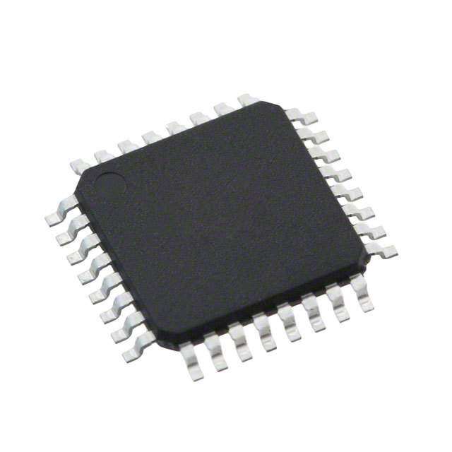
| 描述 | IC DSC 16BIT 66KB FLASH 64TQFP数字信号处理器和控制器 - DSP, DSC 30MHz 66KB Flash |
| EEPROM容量 | 1K x 8 |
| 产品分类 | |
| I/O数 | 52 |
| 品牌 | Microchip Technology |
| 产品手册 | |
| 产品图片 |
|
| rohs | 符合RoHS无铅 / 符合限制有害物质指令(RoHS)规范要求 |
| 产品系列 | 嵌入式处理器和控制器,数字信号处理器和控制器 - DSP, DSC,Microchip Technology DSPIC30F5011-30I/PTdsPIC™ 30F |
| 数据手册 | http://www.microchip.com/mymicrochip/filehandler.aspx?ddocname=en505487http://www.microchip.com/mymicrochip/filehandler.aspx?ddocname=en019521点击此处下载产品Datasheet点击此处下载产品Datasheethttp://www.microchip.com/mymicrochip/filehandler.aspx?ddocname=en022175http://www.microchip.com/mymicrochip/filehandler.aspx?ddocname=en533763http://www.microchip.com/mymicrochip/filehandler.aspx?ddocname=en012562http://www.microchip.com/mymicrochip/filehandler.aspx?ddocname=en528221http://www.microchip.com/mymicrochip/filehandler.aspx?ddocname=en537414http://www.microchip.com/mymicrochip/filehandler.aspx?ddocname=en540880 |
| 产品型号 | DSPIC30F5011-30I/PT |
| PCN设计/规格 | http://www.microchip.com/mymicrochip/NotificationDetails.aspx?id=5612&print=view |
| RAM容量 | 4K x 8 |
| 产品 | DSCs |
| 产品培训模块 | http://www.digikey.cn/PTM/IndividualPTM.page?site=cn&lang=zhs&ptm=2046 |
| 产品目录页面 | |
| 产品种类 | 数字信号处理器和控制器 - DSP, DSC |
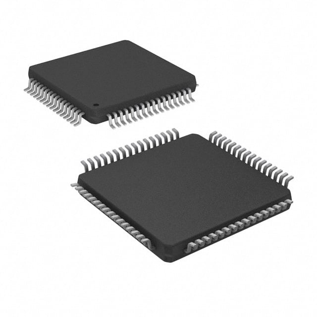
| 供应商器件封装 | 64-TQFP(10x10) |
| 其它名称 | DSPIC30F501130IPT |
| 包装 | 托盘 |
| 可编程输入/输出端数量 | 52 |
| 商标 | Microchip Technology |
| 处理器系列 | dsPIC30F |
| 外设 | AC'97,欠压检测/复位,I²S,LVD,POR,PWM,WDT |
| 安装风格 | SMD/SMT |
| 定时器数量 | 5 Timer |
| 封装 | Tray |
| 封装/外壳 | 64-TQFP |
| 封装/箱体 | TQFP-64 |
| 工作温度 | -40°C ~ 85°C |
| 工厂包装数量 | 160 |
| 振荡器类型 | 内部 |
| 接口类型 | CAN/I2C/SPI/UART |
| 数据RAM大小 | 4 kB |
| 数据总线宽度 | 16 bit |
| 数据转换器 | A/D 16x12b |
| 最大工作温度 | + 85 C |
| 最大时钟频率 | 30 MHz |
| 最小工作温度 | - 40 C |
| 标准包装 | 160 |
| 核心 | dsPIC |
| 核心处理器 | dsPIC |
| 核心尺寸 | 16-位 |
| 片上ADC | Yes |
| 电压-电源(Vcc/Vdd) | 2.5 V ~ 5.5 V |
| 程序存储器大小 | 96 kB |
| 程序存储器类型 | Flash |
| 程序存储容量 | 66KB(22K x 24) |
| 类型 | dsPIC30 |
| 系列/芯体 | dsPIC30 |
| 输入/输出端数量 | 52 I/O |
| 连接性 | CAN, I²C, SPI, UART/USART |
| 速度 | 30 MIP |
| 配用 | /product-detail/zh/AC164319/AC164319-ND/665648 |


- 商务部:美国ITC正式对集成电路等产品启动337调查
- 曝三星4nm工艺存在良率问题 高通将骁龙8 Gen1或转产台积电
- 太阳诱电将投资9.5亿元在常州建新厂生产MLCC 预计2023年完工
- 英特尔发布欧洲新工厂建设计划 深化IDM 2.0 战略
- 台积电先进制程称霸业界 有大客户加持明年业绩稳了
- 达到5530亿美元!SIA预计今年全球半导体销售额将创下新高
- 英特尔拟将自动驾驶子公司Mobileye上市 估值或超500亿美元
- 三星加码芯片和SET,合并消费电子和移动部门,撤换高东真等 CEO
- 三星电子宣布重大人事变动 还合并消费电子和移动部门
- 海关总署:前11个月进口集成电路产品价值2.52万亿元 增长14.8%


PDF Datasheet 数据手册内容提取
dsPIC30F5011/5013 Data Sheet High-Performance, 16-bit Digital Signal Controllers © 2011 Microchip Technology Inc. DS70116J
Note the following details of the code protection feature on Microchip devices: • Microchip products meet the specification contained in their particular Microchip Data Sheet. • Microchip believes that its family of products is one of the most secure families of its kind on the market today, when used in the intended manner and under normal conditions. • There are dishonest and possibly illegal methods used to breach the code protection feature. All of these methods, to our knowledge, require using the Microchip products in a manner outside the operating specifications contained in Microchip’s Data Sheets. Most likely, the person doing so is engaged in theft of intellectual property. • Microchip is willing to work with the customer who is concerned about the integrity of their code. • Neither Microchip nor any other semiconductor manufacturer can guarantee the security of their code. Code protection does not mean that we are guaranteeing the product as “unbreakable.” Code protection is constantly evolving. We at Microchip are committed to continuously improving the code protection features of our products. Attempts to break Microchip’s code protection feature may be a violation of the Digital Millennium Copyright Act. If such acts allow unauthorized access to your software or other copyrighted work, you may have a right to sue for relief under that Act. Information contained in this publication regarding device Trademarks applications and the like is provided only for your convenience The Microchip name and logo, the Microchip logo, dsPIC, and may be superseded by updates. It is your responsibility to KEELOQ, KEELOQ logo, MPLAB, PIC, PICmicro, PICSTART, ensure that your application meets with your specifications. PIC32 logo, rfPIC and UNI/O are registered trademarks of MICROCHIP MAKES NO REPRESENTATIONS OR Microchip Technology Incorporated in the U.S.A. and other WARRANTIES OF ANY KIND WHETHER EXPRESS OR countries. IMPLIED, WRITTEN OR ORAL, STATUTORY OR OTHERWISE, RELATED TO THE INFORMATION, FilterLab, Hampshire, HI-TECH C, Linear Active Thermistor, INCLUDING BUT NOT LIMITED TO ITS CONDITION, MXDEV, MXLAB, SEEVAL and The Embedded Control QUALITY, PERFORMANCE, MERCHANTABILITY OR Solutions Company are registered trademarks of Microchip FITNESS FOR PURPOSE. Microchip disclaims all liability Technology Incorporated in the U.S.A. arising from this information and its use. Use of Microchip Analog-for-the-Digital Age, Application Maestro, CodeGuard, devices in life support and/or safety applications is entirely at dsPICDEM, dsPICDEM.net, dsPICworks, dsSPEAK, ECAN, the buyer’s risk, and the buyer agrees to defend, indemnify and ECONOMONITOR, FanSense, HI-TIDE, In-Circuit Serial hold harmless Microchip from any and all damages, claims, Programming, ICSP, Mindi, MiWi, MPASM, MPLAB Certified suits, or expenses resulting from such use. No licenses are logo, MPLIB, MPLINK, mTouch, Omniscient Code conveyed, implicitly or otherwise, under any Microchip Generation, PICC, PICC-18, PICDEM, PICDEM.net, PICkit, intellectual property rights. PICtail, REAL ICE, rfLAB, Select Mode, Total Endurance, TSHARC, UniWinDriver, WiperLock and ZENA are trademarks of Microchip Technology Incorporated in the U.S.A. and other countries. SQTP is a service mark of Microchip Technology Incorporated in the U.S.A. All other trademarks mentioned herein are property of their respective companies. © 2011, Microchip Technology Incorporated, Printed in the U.S.A., All Rights Reserved. Printed on recycled paper. ISBN: 978-1-60932-843-6 Microchip received ISO/TS-16949:2002 certification for its worldwide headquarters, design and wafer fabrication facilities in Chandler and Tempe, Arizona; Gresham, Oregon and design centers in California and India. The Company’s quality system processes and procedures are for its PIC® MCUs and dsPIC® DSCs, KEELOQ® code hopping devices, Serial EEPROMs, microperipherals, nonvolatile memory and analog products. In addition, Microchip’s quality system for the design and manufacture of development systems is ISO 9001:2000 certified. DS70116J-page 2 © 2011 Microchip Technology Inc.
dsPIC30F5011/5013 High-Performance, Digital Signal Controllers Peripheral Features: Note: This data sheet summarizes features of this group ofdsPIC30F devices and is not • High-current sink/source I/O pins: 25mA/25mA intended to be a complete reference • Five 16-bit timers/counters; optionally pair up source. For more information on the CPU, 16-bit timers into 32-bit timer modules peripherals, register descriptions and • 16-bit Capture input functions general device functionality, refer to the • 16-bit Compare/PWM output functions “dsPIC30F Family Reference Manual” • Data Converter Interface (DCI) supports common (DS70046). For more information on the audio codec protocols, including I2S and AC’97 device instruction set and programming, refer to the “16-bit MCU and DSC Pro- • 3-wire SPI modules (supports four Frame modes) grammer’s Reference Manual” • I2C™ module supports Multi-Master/Slave mode (DS70157). and 7-bit/10-bit addressing • Two addressable UART modules with FIFO High-Performance Modified RISC CPU: buffers • Two CAN bus modules compliant with CAN 2.0B • Modified Harvard architecture standard • C compiler optimized instruction set architecture • Flexible addressing modes Analog Features: • 83 base instructions • 12-bit Analog-to-Digital Converter (ADC) with: • 24-bit wide instructions, 16-bit wide data path - 200 ksps conversion rate • 66 Kbytes on-chip Flash program space - Up to 16 input channels • 4 Kbytes of on-chip data RAM - Conversion available during Sleep and Idle • 1 Kbyte of nonvolatile data EEPROM • Programmable Low-Voltage Detection (PLVD) • 16 x 16-bit working register array • Programmable Brown-out Detection and Reset • Up to 30 MIPS operation: generation - DC to 40MHz external clock input - 4MHz-10MHz oscillator input with Special Microcontroller Features: PLL active (4x, 8x, 16x) • Enhanced Flash program memory: • Up to 41 interrupt sources: - 10,000 erase/write cycle (min.) for - Eight user selectable priority levels industrial temperature range, 100K (typical) - Five external interrupt sources • Data EEPROM memory: - Four processor traps - 100,000 erase/write cycle (min.) for industrial temperature range, 1M (typical) DSP Features: • Self-reprogrammable under software control • Dual data fetch • Power-on Reset (POR), Power-up Timer (PWRT) • Modulo and Bit-Reversed modes and Oscillator Start-up Timer (OST) • Two 40-bit wide accumulators with optional • Flexible Watchdog Timer (WDT) with on-chip saturation logic low- power RC oscillator for reliable operation • 17-bit x 17-bit single cycle hardware fractional/ • Fail-Safe Clock Monitor operation: integer multiplier - Detects clock failure and switches to on-chip • All DSP instructions are single cycle low-power RC oscillator - Multiply-Accumulate (MAC) operation • Programmable code protection • Single cycle ±16 shift • In-Circuit Serial Programming™ (ICSP™) programming capability • Selectable Power Management modes: - Sleep, Idle and Alternate Clock modes © 2011 Microchip Technology Inc. DS70116J-page 3
dsPIC30F5011/5013 CMOS Technology: • Low-power, high-speed Flash technology • Wide operating voltage range (2.5V to 5.5V) • Industrial and Extended temperature ranges • Low power consumption TABLE 1: dsPIC30F5011/5013 CONTROLLER FAMILY Device Pins BPyrtoegsraImns tMruecmtioornys SBRytAeMs EEBPyRteOsM T16im-beirt InCpaupt COoPmuWtppM/uStt d InCteordfaecce A2/0D0 1 k2s-pbsit UART SPI 2™IC CAN dsPIC30F5011 64 66K 22K 4096 1024 5 8 8 AC’97, I2S 16 ch 2 2 1 2 dsPIC30F5013 80 66K 22K 4096 1024 5 8 8 AC’97, I2S 16 ch 2 2 1 2 DS70116J-page 4 © 2011 Microchip Technology Inc.
dsPIC30F5011/5013 Pin Diagrams 64-Pin TQFP 54 D7D64/RD3/RD RD1 CSDO/RG13CSDI/RG12CSCK/RG14C2RX/RG0C2TX/RG1C1TX/RF1C1RX/RF0VDDVSSOC8/CN16/ROC7/CN15/ROC6/IC6/CN1OC5/IC5/CN1OC4/RD3OC3/RD2EMUD2/OC2/ 4321098765432109 6666655555555554 COFS/RG15 1 48 EMUC1/SOSCO/T1CK/CN0/RC14 T2CK/RC1 2 47 EMUD1/SOSCI/T4CK/CN1/RC13 T3CK/RC2 3 46 EMUC2/OC1/RD0 SCK2/CN8/RG6 4 45 IC4/INT4/RD11 SDI2/CN9/RG7 5 44 IC3/INT3/RD10 SDO2/CN10/RG8 6 43 IC2/INT2/RD9 MCLR 7 42 IC1/INT1/RD8 SS2/CN11/RG9 8 41 VSS dsPIC30F5011 VSS 9 40 OSC2/CLKO/RC15 VDD 10 39 OSC1/CLKI AN5/IC8/CN7/RB5 11 38 VDD AN4/IC7/CN6/RB4 12 37 SCL/RG2 AN3/CN5/RB3 13 36 SDA/RG3 AN2/SS1/LVDIN/CN4/RB2 14 35 EMUC3/SCK1/INT0/RF6 AN1/VREF-/CN3/RB1 15 34 U1RX/SDI1/RF2 AN0/VREF+/CN2/RB0 16 33 EMUD3/U1TX/SDO1/RF3 7890123456789012 1112222222222333 67 D S8901 S D234545 BB D SBB11 S D1111FF RRVVRRBBVVBBBBRR C/AN6/OCFA/D/EMUD/AN7/AAAN8/AN9/AN10/RAN11/R AN12/RAN13/RAN14/ROCFB/CN12/RU2RX/CN17/U2TX/CN18/ MUPG 15/ E N C/ A G P © 2011 Microchip Technology Inc. DS70116J-page 5
dsPIC30F5011/5013 Pin Diagrams (Continued) 80-Pin TQFP 1 D7 D6 D5D4 13 RD CSDO/RG13 CSDI/RG12 CSCK/RG14 CN23/RA7 CN22/RA6C2RX/RG0 C2TX/RG1 C1TX/RF1 C1RX/RF0 VDD VSS OC8/CN16/R OC7/CN15/R OC6/CN14/ROC5/CN13/R IC6/CN19/RD IC5/RD12 OC4/RD3 OC3/RD2 EMUD2/OC2/ 0 9 8 7 6 5 4 3 2 1 0 9 8 7 65 4 3 2 1 8 7 7 7 7 7 7 7 7 7 7 6 6 6 66 6 6 6 6 60 EMUC1/SOSCO/T1CK/CN0/RC14 COFS/RG15 1 59 EMUD1/SOSCI/CN1/RC13 T2CK/RC1 2 58 EMUC2/OC1/RD0 T3CK/RC2 3 57 IC4/RD11 T4CK/RC3 4 56 IC3/RD10 T5CK/RC4 5 55 IC2/RD9 SCK2/CN8/RG6 6 SDI2/CN9/RG7 7 54 IC1/RD8 SDO2/CN10/RG8 8 53 INT4/RA15 MCLR 9 52 INT3/RA14 SS2/CN11/RG9 10 dsPIC30F5013 51 VSS VSS 11 50 OSC2/CLKO/RC15 VDD 12 49 OSC1/CLKI INT1/RA12 13 48 VDD INT2/RA13 14 47 SCL/RG2 AN5/CN7/RB5 15 46 SDA/RG3 AN4/CN6/RB4 16 45 EMUC3/SCK1/INT0/RF6 AN3/CN5/RB3 17 44 SDI1/RF7 AN2/SS1/LVDIN/CN4/RB2 18 43 EMUD3/SDO1/RF8 PGC/EMUC/AN1/CN3/RB1 19 42 U1RX/RF2 PGD/EMUD/AN0/CN2/RB0 20 41 U1TX/RF3 1 2 3 4 5 6 7 8 9 0 1 2 3 4 5 6 7 8 9 0 2 2 2 2 2 2 2 2 2 3 3 3 3 3 3 3 3 3 3 4 6 7 9 0 D S 8 9 0 1 S D 2 3 4 5 4 5 4 5 B B A 1 D S B B 1 1 S D 1 1 1 1 1 1 F F R R R A V V R R B B V V B B B B D D R R N6/OCFA/ AN7/ V-/REF V+/RREF A A AN8/ AN9/ AN10/R AN11/R AN12/R AN13/R AN14/R B/CN12/R 7/CN20/R 8/CN21/R RX/CN17/ TX/CN18/ A CF IC IC U2 U2 O 5/ 1 N A DS70116J-page 6 © 2011 Microchip Technology Inc.
dsPIC30F5011/5013 Table of Contents 1.0 Device Overview..........................................................................................................................................................................9 2.0 CPU Architecture Overview........................................................................................................................................................15 3.0 Memory Organization.................................................................................................................................................................23 4.0 Interrupts....................................................................................................................................................................................35 5.0 Address Generator Units............................................................................................................................................................41 6.0 Flash Program Memory..............................................................................................................................................................47 7.0 Data EEPROM Memory.............................................................................................................................................................53 8.0 I/O Ports.....................................................................................................................................................................................57 9.0 Timer1 Module...........................................................................................................................................................................63 10.0 Timer2/3 Module........................................................................................................................................................................67 11.0 Timer4/5 Module .......................................................................................................................................................................73 12.0 Input Capture Module.................................................................................................................................................................77 13.0 Output Compare Module............................................................................................................................................................81 14.0 SPI™ Module.............................................................................................................................................................................87 15.0 I2C™ Module.............................................................................................................................................................................91 16.0 Universal Asynchronous Receiver Transmitter (UART) Module................................................................................................99 17.0 CAN Module.............................................................................................................................................................................107 18.0 Data Converter Interface (DCI) Module....................................................................................................................................117 19.0 12-bit Analog-to-Digital Converter (ADC) Module....................................................................................................................127 20.0 System Integration...................................................................................................................................................................137 21.0 Instruction Set Summary..........................................................................................................................................................151 22.0 Development Support...............................................................................................................................................................159 23.0 Electrical Characteristics..........................................................................................................................................................163 24.0 Packaging Information..............................................................................................................................................................203 Index..................................................................................................................................................................................................209 The Microchip Web Site.....................................................................................................................................................................215 Customer Change Notification Service..............................................................................................................................................215 Customer Support..............................................................................................................................................................................215 Reader Response..............................................................................................................................................................................216 Product Identification System............................................................................................................................................................217 TO OUR VALUED CUSTOMERS It is our intention to provide our valued customers with the best documentation possible to ensure successful use of your Microchip products. To this end, we will continue to improve our publications to better suit your needs. Our publications will be refined and enhanced as new volumes and updates are introduced. If you have any questions or comments regarding this publication, please contact the Marketing Communications Department via E-mail at docerrors@microchip.com or fax the Reader Response Form in the back of this data sheet to (480) 792-4150. We welcome your feedback. Most Current Data Sheet To obtain the most up-to-date version of this data sheet, please register at our Worldwide Web site at: http://www.microchip.com You can determine the version of a data sheet by examining its literature number found on the bottom outside corner of any page. The last character of the literature number is the version number, (e.g., DS30000A is version A of document DS30000). Errata An errata sheet, describing minor operational differences from the data sheet and recommended workarounds, may exist for current devices. As device/documentation issues become known to us, we will publish an errata sheet. The errata will specify the revision of silicon and revision of document to which it applies. To determine if an errata sheet exists for a particular device, please check with one of the following: • Microchip’s Worldwide Web site; http://www.microchip.com • Your local Microchip sales office (see last page) When contacting a sales office, please specify which device, revision of silicon and data sheet (include literature number) you are using. Customer Notification System Register on our web site at www.microchip.com to receive the most current information on all of our products. © 2011 Microchip Technology Inc. DS70116J-page 7
dsPIC30F5011/5013 NOTES: DS70116J-page 8 © 2011 Microchip Technology Inc.
dsPIC30F5011/5013 1.0 DEVICE OVERVIEW Note: This data sheet summarizes features of this group ofdsPIC30F devices and is not intended to be a complete reference source. For more information on the CPU, peripherals, register descriptions and general device functionality, refer to the “dsPIC30F Family Reference Manual” (DS70046). For more information on the device instruction set and programming, refer to the “16-bit MCU and DSC Programmer’s Reference Manual” (DS70157). This document contains specific information for the dsPIC30F5011/5013 Digital Signal Controller (DSC) devices. The dsPIC30F5011/5013 devices contain extensive Digital Signal Processor (DSP) functionality within a high-performance 16-bit microcontroller (MCU) architecture. Figure1-1 and Figure1-2 show device block diagrams for dsPIC30F5011 and dsPIC30F5013, respectively. © 2011 Microchip Technology Inc. DS70116J-page 9
dsPIC30F5011/5013 FIGURE 1-1: dsPIC30F5011 BLOCK DIAGRAM Y Data Bus X Data Bus 16 16 16 16 Interrupt Data Latch Data Latch Controller PDSaVta &A cTcaebsles Y Data X Data 24Control Block 8 16 RAM RAM (2 Kbytes) (2 Kbytes) AN0/VREF+/CN2/RB0 Address Address 16 AN1/VREF-/CN3/RB1 24 Latch Latch AN2/SS1/LVDIN/CN4/RB2 16 16 16 AN3/CN5/RB3 AN4/IC7/CN6/RB4 24 X RAGU Y AGU AN5/IC8/CN7/RB5 PCU PCH PCL X WAGU PGC/EMUC/AN6/OCFA/RB6 Program Counter PGD/EMUD/AN7/RB7 Address Latch CSotanctrkol CLoonotprol AN8/RB8 Program Logic Logic AN9/RB9 Memory AN10/RB10 (66 Kbytes) AN11/RB11 Data EEPROM AN12/RB12 (1 Kbyte) Effective Address AN13/RB13 Data Latch 16 AN14/RB14 AN15/OCFB/CN12/RB15 ROM Latch 16 PORTB 24 IR T2CK/RC1 16 T3CK/RC2 16 EMUD1/SOSCI/T4CK/CN1/RC13 16 x 16 EMUC1/SOSCO/T1CK/CN0/RC14 W Reg Array OSC2/CLKO/RC15 Decode Instruction PORTC Decode & 16 16 Control EMUC2/OC1/RD0 Ctoo Vnatrroiol uSsig Bnlaolcsk s Power-up E DngSiPne D Uivnidite EOOMCCU34//DRR2DD/23OC2/RD1 Timer OC5/IC5/CN13/RD4 OSC1/CLKI Timing Oscillator OC6/IC6/CN14/RD5 Generation Start-up Timer OC7/CN15/RD6 ALU<16> OC8/CN16/RD7 POR/BOR IC1/INT1/RD8 IC2/INT2/RD9 MCLR Watchdog 16 16 IC3/INT3/RD10 Timer IC4/INT4/RD11 Low-Voltage VDD, VSS Detect PORTD AVDD, AVSS CAN1, Input O utput CAN2 12-bit ADC C Mapotduurele CMoom dpualere I2C™ C1RX/RF0 C1TX/RF1 U1RX/SDI1/RF2 EMUD3/U1TX/SDO1/RF3 U2RX/CN17/RF4 U2TX/CN18/RF5 Timers DCI SPI1, UART1, EMUC3/SCK1/INT0/RF6 SPI2 UART2 PORTF C2RX/RG0 C2TX/RG1 SCL/RG2 SDA/RG3 SCK2/CN8/RG6 SDI2/CN9/RG7 SDO2/CN10/RG8 SS2/CN11/RG9 CSDI/RG12 CSDO/RG13 CSCK/RG14 COFS/RG15 PORTG DS70116J-page 10 © 2011 Microchip Technology Inc.
dsPIC30F5011/5013 FIGURE 1-2: dsPIC30F5013 BLOCK DIAGRAM CN22/RA6 Y Data Bus CN23/RA7 X Data Bus VREF-/RA9 16 16 16 VREF+/RA10 16 INT1/RA12 Interrupt Data Latch Data Latch INT2/RA13 Controller DPaStVa A&c Tcaebslse Y Data X Data INT3/RA14 24Control Block 8 16 RAM RAM INT4/RA15 (2A Kddbryetesss) (2A dKdbryetsess) 16 PORTA 24 Latch Latch PGD/EMUD/AN0/CN2/RB0 16 16 16 PGC/EMUC/AN1/CN3/RB1 AN2/SS1/LVDIN/CN4/RB2 24 X RAGU Y AGU AN3/CN5/RB3 PCU PCH PCL X WAGU AN4/CN6/RB4 Program Counter AN5/CN7/RB5 Address Latch CSotanctrkol CLoonotrpol AN6/OCFA/RB6 Program Memory Logic Logic AN7/RB7 (66 Kbytes) AN8/RB8 AN9/RB9 Data EEPROM AN10/RB10 (1 Kbyte) Effective Address AN11/RB11 Data Latch 16 AN12/RB12 AN13/RB13 AN14/RB14 ROM Latch 16 AN15/OCFB/CN12/RB15 24 PORTB T2CK/RC1 IR T3CK/RC2 16 T4CK/RC3 16 T5CK/RC4 16 x 16 EMUD1/SOSCI/CN1/RC13 W Reg Array EMUC1/SOSCO/T1CK/CN0/RC14 Decode OSC2/CLKO/RC15 Instruction PORTC Decode & 16 16 Control EMUC2/OC1/RD0 EMUD2/OC2/RD1 OC3/RD2 Control Signals DSP Divide OC4/RD3 to Various Blocks Power-up Engine Unit OC5/CN13/RD4 Timer OC6/CN14/RD5 OSC1/CLKI GeTnimeriantgion StaOrts-ucipll aTtiomrer OOCC78//CCNN1156//RRDD67 IC1/RD8 POR/BOR ALU<16> IC2/RD9 IC3/RD10 MCLR WaTticmhedrog 16 16 IICC45//RRDD1112 IC6/CN19/RD13 Low-Voltage IC7/CN20/RD14 VDD, VSS Detect IC8/CN21/RD15 AVDD, AVSS PORTD CAN1, Input O utput C1RX/RF0 CAN2 12-bit ADC Capture Com pare I2C™ C1TX/RF1 Module Module U1RX/RF2 U1TX/RF3 U2RX/CN17/RF4 U2TX/CN18/RF5 EMUC3/SCK1/INT0/RF6 SDI1/RF7 Timers DCI SPI1, UART1, EMUD3/SDO1/RF8 SPI2 UART2 PORTF C2RX/RG0 C2TX/RG1 SCL/RG2 SDA/RG3 SCK2/CN8/RG6 SDI2/CN9/RG7 SDO2/CN10/RG8 SS2/CN11/RG9 CSDI/RG12 CSDO/RG13 CSCK/RG14 COFS/RG15 PORTG © 2011 Microchip Technology Inc. DS70116J-page 11
dsPIC30F5011/5013 Table1-1 provides a brief description of device I/O pin- outs and the functions that may be multiplexed to a port pin. Multiple functions may exist on one port pin. When multiplexing occurs, the peripheral module’s functional requirements may force an override of the data direction of the port pin. TABLE 1-1: PINOUT I/O DESCRIPTIONS Pin Buffer Pin Name Description Type Type AN0-AN15 I Analog Analog input channels. AN0 and AN1 are also used for device programming data and clock inputs, respectively. AVDD P P Positive supply for analog module. This pin must be connected at all times. AVSS P P Ground reference for analog module. This pin must be connected at all times. CLKI I ST/CMOS External clock source input. Always associated with OSC1 pin function. CLKO O — Oscillator crystal output. Connects to crystal or resonator in Crystal Oscillator mode. Optionally functions as CLKO in RC and EC modes. Always associated with OSC2 pin function. CN0-CN23 I ST Input change notification inputs. Can be software programmed for internal weak pull-ups on all inputs. COFS I/O ST Data Converter Interface Frame Synchronization pin. CSCK I/O ST Data Converter Interface Serial Clock input/output pin. CSDI I ST Data Converter Interface Serial data input pin. CSDO O — Data Converter Interface Serial data output pin. C1RX I ST CAN1 Bus Receive pin. C1TX O — CAN1 Bus Transmit pin. C2RX I ST CAN2 Bus Receive pin. C2TX O — CAN2 Bus Transmit pin EMUD I/O ST ICD Primary Communication Channel data input/output pin. EMUC I/O ST ICD Primary Communication Channel clock input/output pin. EMUD1 I/O ST ICD Secondary Communication Channel data input/output pin. EMUC1 I/O ST ICD Secondary Communication Channel clock input/output pin. EMUD2 I/O ST ICD Tertiary Communication Channel data input/output pin. EMUC2 I/O ST ICD Tertiary Communication Channel clock input/output pin. EMUD3 I/O ST ICD Quaternary Communication Channel data input/output pin. EMUC3 I/O ST ICD Quaternary Communication Channel clock input/output pin. IC1-IC8 I ST Capture inputs 1 through 8. INT0 I ST External interrupt 0. INT1 I ST External interrupt 1. INT2 I ST External interrupt 2. INT3 I ST External interrupt 3. INT4 I ST External interrupt 4. LVDIN I Analog Low-Voltage Detect Reference Voltage input pin. MCLR I/P ST Master Clear (Reset) input or programming voltage input. This pin is an active low Reset to the device. OCFA I ST Compare Fault A input (for Compare channels 1, 2, 3 and 4). OCFB I ST Compare Fault B input (for Compare channels 5, 6, 7 and 8). OC1-OC8 O — Compare outputs 1 through 8. Legend: CMOS = CMOS compatible input or output Analog = Analog input ST = Schmitt Trigger input with CMOS levels O = Output I = Input P = Power DS70116J-page 12 © 2011 Microchip Technology Inc.
dsPIC30F5011/5013 TABLE 1-1: PINOUT I/O DESCRIPTIONS (CONTINUED) Pin Buffer Pin Name Description Type Type OSC1 I ST/CMOS Oscillator crystal input. ST buffer when configured in RC mode; CMOS otherwise. OSC2 I/O — Oscillator crystal output. Connects to crystal or resonator in Crystal Oscillator mode. Optionally functions as CLKO in RC and EC modes. PGD I/O ST In-Circuit Serial Programming™ data input/output pin. PGC I ST In-Circuit Serial Programming clock input pin. RA6-RA7 I/O ST PORTA is a bidirectional I/O port. RA9-RA10 I/O ST RA12-RA15 I/O ST RB0-RB15 I/O ST PORTB is a bidirectional I/O port. RC1-RC4 I/O ST PORTC is a bidirectional I/O port. RC13-RC15 I/O ST RD0-RD15 I/O ST PORTD is a bidirectional I/O port. RF0-RF8 I/O ST PORTF is a bidirectional I/O port. RG0-RG3 I/O ST PORTG is a bidirectional I/O port. RG6-RG9 I/O ST RG12-RG15 I/O ST SCK1 I/O ST Synchronous serial clock input/output for SPI1. SDI1 I ST SPI1 Data In. SDO1 O — SPI1 Data Out. SS1 I ST SPI1 Slave Synchronization. SCK2 I/O ST Synchronous serial clock input/output for SPI2. SDI2 I ST SPI2 Data In. SDO2 O — SPI2 Data Out. SS2 I ST SPI2 Slave Synchronization. SCL I/O ST Synchronous serial clock input/output for I2C™. SDA I/O ST Synchronous serial data input/output for I2C. SOSCO O — 32 kHz low-power oscillator crystal output. SOSCI I ST/CMOS 32 kHz low-power oscillator crystal input. ST buffer when configured in RC mode; CMOS otherwise. T1CK I ST Timer1 external clock input. T2CK I ST Timer2 external clock input. T3CK I ST Timer3 external clock input. T4CK I ST Timer4 external clock input. T5CK I ST Timer5 external clock input. U1RX I ST UART1 Receive. U1TX O — UART1 Transmit. U1ARX I ST UART1 Alternate Receive. U1ATX O — UART1 Alternate Transmit. U2RX I ST UART2 Receive. U2TX O — UART2 Transmit. VDD P — Positive supply for logic and I/O pins. VSS P — Ground reference for logic and I/O pins. VREF+ I Analog Analog Voltage Reference (High) input. VREF- I Analog Analog Voltage Reference (Low) input. Legend: CMOS = CMOS compatible input or output Analog = Analog input ST = Schmitt Trigger input with CMOS levels O = Output I = Input P = Power © 2011 Microchip Technology Inc. DS70116J-page 13
dsPIC30F5011/5013 NOTES: DS70116J-page 14 © 2011 Microchip Technology Inc.
dsPIC30F5011/5013 2.0 CPU ARCHITECTURE There are two methods of accessing data stored in OVERVIEW program memory: • The upper 32 Kbytes of data space memory can Note: This data sheet summarizes features of be mapped into the lower half (user space) of pro- this group ofdsPIC30F devices and is not gram space at any 16K program word boundary, intended to be a complete reference defined by the 8-bit Program Space Visibility source. For more information on the CPU, Page (PSVPAG) register. This lets any instruction peripherals, register descriptions and access program space as if it were data space, general device functionality, refer to the with a limitation that the access requires an addi- “dsPIC30F Family Reference Manual” tional cycle. Moreover, only the lower 16 bits of (DS70046). For more information on the each instruction word can be accessed using this device instruction set and programming, method. refer to the “16-bit MCU and DSC • Linear indirect access of 32K word pages within Programmer’s Reference Manual” program space is also possible using any working (DS70157). register, via table read and write instructions. Table read and write instructions can be used to 2.1 Core Overview access all 24 bits of an instruction word. Overhead-free circular buffers (modulo addressing) are This section contains a brief overview of the CPU supported in both X and Y address spaces. This is architecture of the dsPIC30F. For additional hard- primarily intended to remove the loop overhead for wareand programming information, please refer to DSP algorithms. the“dsPIC30F Family Reference Manual” (DS70046) and the“16-bit MCU and DSC Programmer’s The X AGU also supports bit-reversed addressing on Reference Manual” (DS70157), respectively. destination effective addresses to greatly simplify input or output data reordering for radix-2 FFT algorithms. The core has a 24-bit instruction word. The Program Refer to Section5.0 “Address Generator Units” for Counter (PC) is 23 bits wide with the Least Significant details on modulo and bit-reversed addressing. bit (LSb) always clear (refer to Section3.1 “Program Address Space”), and the Most Significant bit (MSb) The core supports Inherent (no operand), Relative, is ignored during normal program execution, except for Literal, Memory Direct, Register Direct, Register certain specialized instructions. Thus, the PC can Indirect, Register Offset and Literal Offset Addressing address up to 4M instruction words of user program modes. Instructions are associated with predefined space. An instruction prefetch mechanism is used to Addressing modes, depending upon their functional help maintain throughput. Program loop constructs, requirements. free from loop count management overhead, are sup- For most instructions, the core is capable of executing ported using the DO and REPEAT instructions, both of a data (or program data) memory read, a working reg- which are interruptible at any point. ister (data) read, a data memory write and a program The working register array consists of 16 x 16-bit regis- (instruction) memory read per instruction cycle. As a ters, each of which can act as data, address or offset result, 3-operand instructions are supported, allowing registers. One working register (W15) operates as a C=A + B operations to be executed in a single cycle. software Stack Pointer for interrupts and calls. A DSP engine has been included to significantly The data space is 64 Kbytes (32K words) and is split enhance the core arithmetic capability and throughput. into two blocks, referred to as X and Y data memory. It features a high-speed 17-bit by 17-bit multiplier, a Each block has its own independent Address Genera- 40-bit ALU, two 40-bit saturating accumulators and a tion Unit (AGU). Most instructions operate solely 40-bit bidirectional barrel shifter. Data in the accumula- through the X memory, AGU, which provides the tor or any working register can be shifted up to 15 bits appearance of a single unified data space. The right, or 16 bits left in a single cycle. The DSP instruc- Multiply-Accumulate (MAC) class of dual source DSP tions operate seamlessly with all other instructions and instructions operate through both the X and Y AGUs, have been designed for optimal real-time performance. splitting the data address space into two parts (see The MAC class of instructions can concurrently fetch Section3.2 “Data Address Space”). The X and Y two data operands from memory while multiplying two data space boundary is device specific and cannot be W registers. To enable this concurrent fetching of data altered by the user. Each data word consists of 2 bytes, operands, the data space has been split for these and most instructions can address data either as words instructions and linear for all others. This has been or bytes. achieved in a transparent and flexible manner, by ded- icating certain working registers to each address space for the MAC class of instructions. © 2011 Microchip Technology Inc. DS70116J-page 15
dsPIC30F5011/5013 The core does not support a multi-stage instruction 2.2.1 SOFTWARE STACK POINTER/ pipeline. However, a single stage instruction prefetch FRAME POINTER mechanism is used, which accesses and partially The dsPIC® DSC devices contain a software stack. decodes instructions a cycle ahead of execution, in W15 is the dedicated software Stack Pointer (SP), and order to maximize available execution time. Most will be automatically modified by exception processing instructions execute in a single cycle with certain and subroutine calls and returns. However, W15 can be exceptions. referenced by any instruction in the same manner as all The core features a vectored exception processing other W registers. This simplifies the reading, writing structure for traps and interrupts, with 62 independent and manipulation of the Stack Pointer (e.g., creating vectors. The exceptions consist of up to 8 traps (of stack frames). which 4 are reserved) and 54 interrupts. Each interrupt Note: In order to protect against misaligned is prioritized based on a user assigned priority between stack accesses, W15<0> is always clear. 1 and 7 (1 being the lowest priority and 7 being the highest), in conjunction with a predetermined ‘natural W15 is initialized to 0x0800 during a Reset. The user order’. Traps have fixed priorities ranging from 8 to 15. may reprogram the SP during initialization to any location within data space. 2.2 Programmer’s Model W14 has been dedicated as a Stack Frame Pointer as The programmer’s model is shown in Figure2-1 and defined by the LNK and ULNK instructions. However, consists of 16 x 16-bit working registers (W0 through W14 can be referenced by any instruction in the same W15), 2 x 40-bit accumulators (AccA and AccB), manner as all other W registers. STATUS register (SR), Data Table Page register 2.2.2 STATUS REGISTER (TBLPAG), Program Space Visibility Page register (PSVPAG), DO and REPEAT registers (DOSTART, The dsPIC DSC core has a 16-bit STATUS register DOEND, DCOUNT and RCOUNT) and Program Coun- (SR), the LSB of which is referred to as the SR Low ter (PC). The working registers can act as data, byte (SRL) and the MSB as the SR High byte (SRH). address or offset registers. All registers are memory See Figure 2-1 for SR layout. mapped. W0 acts as the W register for file register SRL contains all the MCU ALU operation status flags addressing. (including the Z bit), as well as the CPU Interrupt Prior- Some of these registers have a shadow register asso- ity Level status bits, IPL<2:0> and the Repeat Active ciated with each of them, as shown in Figure2-1. The Status bit, RA. During exception processing, SRL is shadow register is used as a temporary holding register concatenated with the MSB of the PC to form a com- and can transfer its contents to or from its host register plete word value which is then stacked. upon the occurrence of an event. None of the shadow The upper byte of the STATUS register contains the registers are accessible directly. The following rules DSP Adder/Subtracter status bits, the DO Loop Active apply for transfer of registers into and out of shadows. bit (DA) and the Digit Carry (DC) Status bit. • PUSH.S and POP.S W0, W1, W2, W3, SR (DC, N, OV, Z and C bits 2.2.3 PROGRAM COUNTER only) are transferred. The program counter is 23 bits wide; bit 0 is always • DO instruction clear. Therefore, the PC can address up to 4M DOSTART, DOEND, DCOUNT shadows are instruction words. pushed on loop start, and popped on loop end. When a byte operation is performed on a working reg- ister, only the Least Significant Byte (LSB) of the target register is affected. However, a benefit of memory mapped working registers is that both the Least and Most Significant Bytes (MSBs) can be manipulated through byte wide data memory space accesses. DS70116J-page 16 © 2011 Microchip Technology Inc.
dsPIC30F5011/5013 FIGURE 2-1: PROGRAMMER’S MODEL D15 D0 W0/WREG PUSH.S Shadow W1 DO Shadow W2 W3 Legend W4 DSP Operand W5 Registers W6 W7 Working Registers W8 W9 DSP Address Registers W10 W11 W12/DSP Offset W13/DSP Write Back W14/Frame Pointer W15/Stack Pointer SPLIM Stack Pointer Limit Register AD39 AD31 AD15 AD0 DSP AccA Accumulators AccB PC22 PC0 0 Program Counter 7 0 TTBALBPPAAGG Data Table Page Address 7 0 PPSSVVPPAAGG Program Space Visibility Page Address 15 0 RCOUNT REPEAT Loop Counter 15 0 DCOUNT DO Loop Counter 22 0 DOSTART DO Loop Start Address 22 DOEND DO Loop End Address 15 0 CORCON Core Configuration Register OA OB SA SB OAB SAB DA DC IPL2 IPL1 IPL0 RA N OV Z C STATUS Register SRH SRL © 2011 Microchip Technology Inc. DS70116J-page 17
dsPIC30F5011/5013 2.3 Divide Support 2.4 DSP Engine The dsPIC DSC devices feature a 16/16-bit signed The DSP engine consists of a high-speed 17-bit x fractional divide operation, as well as 32/16-bit and 16/ 17-bit multiplier, a barrel shifter and a 40-bit adder/ 16-bit signed and unsigned integer divide operations, in subtracter (with two target accumulators, round and the form of single instruction iterative divides. The saturation logic). following instructions and data sizes are supported: The DSP engine also has the capability to perform • DIVF - 16/16 signed fractional divide inherent accumulator-to-accumulator operations, • DIV.sd - 32/16 signed divide which require no additional data. These instructions are • DIV.ud - 32/16 unsigned divide ADD, SUB and NEG. • DIV.sw - 16/16 signed divide The dsPIC30F is a single-cycle instruction flow archi- • DIV.uw - 16/16 unsigned divide tecture; therefore, concurrent operation of the DSP engine with MCU instruction flow is not possible. The 16/16 divides are similar to the 32/16 (same number However, some MCU ALU and DSP engine resources of iterations), but the dividend is either zero-extended or may be used concurrently by the same instruction (e.g., sign-extended during the first iteration. ED, EDAC). The divide instructions must be executed within a The DSP engine has various options selected through REPEAT loop. Any other form of execution (e.g., a various bits in the CPU Core Configuration register series of discrete divide instructions) will not function (CORCON), as listed below: correctly because the instruction flow depends on • Fractional or integer DSP multiply (IF) RCOUNT. The divide instruction does not automatically set up the RCOUNT value and it must, therefore, be • Signed or unsigned DSP multiply (US) explicitly and correctly specified in the REPEAT instruc- • Conventional or convergent rounding (RND) tion as shown in Table2-2 (REPEAT will execute the tar- • Automatic saturation on/off for AccA (SATA) get instruction {operand value+1} times). The REPEAT • Automatic saturation on/off for AccB (SATB) loop count must be setup for 18 iterations of the DIV/ • Automatic saturation on/off for writes to data DIVF instruction. Thus, a complete divide operation memory (SATDW) requires 19 cycles. • Accumulator Saturation mode selection Note: The divide flow is interruptible. However, (ACCSAT) the user needs to save the context as Note: For CORCON layout, see Table3-3. appropriate. A block diagram of the DSP engine is shown in Figure2-2. TABLE 2-1: DSP INSTRUCTION SUMMARY Algebraic Instruction ACC WB? Operation CLR A = 0 Yes ED A = (x – y)2 No EDAC A = A + (x – y)2 No MAC A = A + (x * y) Yes MAC A = A + x2 No MOVSAC No change in A Yes MPY A = x * y No MPY.N A = – x * y No MSC A = A – x * y Yes TABLE 2-2: DIVIDE INSTRUCTIONS Instruction Function DIVF Signed fractional divide: Wm/Wn → W0; Rem → W1 DIV.sd Signed divide: (Wm+1:Wm)/Wn → W0; Rem → W1 DIV.sw or DIV.s Signed divide: Wm/Wn → W0; Rem → W1 DIV.ud Unsigned divide: (Wm+1:Wm)/Wn → W0; Rem → W1 DIV.uw or DIV.u Unsigned divide: Wm/Wn → W0; Rem → W1 DS70116J-page 18 © 2011 Microchip Technology Inc.
dsPIC30F5011/5013 FIGURE 2-2: DSP ENGINE BLOCK DIAGRAM S a 40 40-bit Accumulator A 40 Round t 16 40-bit Accumulator B u Logic r a Carry/Borrow Out t Saturate e Adder Carry/Borrow In Negate 40 40 40 Barrel 16 Shifter 40 s u B a at D Sign-Extend X s u B a 32 16 at Zero Backfill D Y 32 33 17-bit Multiplier/Scaler 16 16 To/From W Array © 2011 Microchip Technology Inc. DS70116J-page 19
dsPIC30F5011/5013 2.4.1 MULTIPLIER 2.4.2.1 Adder/Subtracter, Overflow and Saturation The 17 x 17-bit multiplier is capable of signed or unsigned operation and can multiplex its output using a The adder/subtracter is a 40-bit adder with an optional scaler to support either 1.31 fractional (Q31) or 32-bit zero input into one side and either true, or complement integer results. Unsigned operands are zero-extended data into the other input. In the case of addition, the into the 17th bit of the multiplier input value. Signed carry/borrow input is active high and the other input is operands are sign-extended into the 17th bit of the mul- true data (not complemented), whereas in the case of tiplier input value. The output of the 17 x 17-bit multi- subtraction, the carry/borrow input is active low and the plier/scaler is a 33-bit value which is sign-extended to other input is complemented. The adder/subtracter 40 bits. Integer data is inherently represented as a generates overflow status bits SA/SB and OA/OB, signed two’s complement value, where the MSB is which are latched and reflected in the STATUS defined as a sign bit. Generally speaking, the range of register: an N-bit two’s complement integer is -2N-1 to 2N-1 – 1. • Overflow from bit 39: this is a catastrophic For a 16-bit integer, the data range is -32768 (0x8000) overflow in which the sign of the accumulator is to 32767 (0x7FFF) including ‘0’. For a 32-bit integer, destroyed. the data range is -2,147,483,648 (0x80000000) to • Overflow into guard bits 32 through 39: this is a 2,147,483,645 (0x7FFF FFFF). recoverable overflow. This bit is set whenever all When the multiplier is configured for fractional multipli- the guard bits are not identical to each other. cation, the data is represented as a two’s complement The adder has an additional saturation block which fraction, where the MSB is defined as a sign bit and the controls accumulator data saturation, if selected. It radix point is implied to lie just after the sign bit (QX for- uses the result of the adder, the overflow status bits mat). The range of an N-bit two’s complement fraction with this implied radix point is -1.0 to (1 – 21-N). For a described above, and the SATA/B (CORCON<7:6>) and ACCSAT (CORCON<4>) mode control bits to 16-bit fraction, the Q15 data range is -1.0 (0x8000) to determine when and to what value to saturate. 0.999969482 (0x7FFF) including ‘0’ and has a preci- sion of 3.01518x10⁻⁵. In Fractional mode, the 16x16 Six STATUS register bits have been provided to multiply operation generates a 1.31 product which has support saturation and overflow; they are: a precision of 4.65661 x 10⁻¹⁰. • OA: AccA overflowed into guard bits The same multiplier is used to support the MCU multi- • OB: AccB overflowed into guard bits ply instructions which include integer 16-bit signed, • SA: AccA saturated (bit 31 overflow and unsigned and mixed sign multiplies. saturation) The MUL instruction may be directed to use byte or or word sized operands. Byte operands will direct a 16-bit AccA overflowed into guard bits and saturated (bit result, and word operands will direct a 32-bit result to 39 overflow and saturation) the specified register(s) in the W array. • SB: AccB saturated (bit 31 overflow and satura- tion) 2.4.2 DATA ACCUMULATORS AND or ADDER/SUBTRACTER AccB overflowed into guard bits and saturated (bit The data accumulator consists of a 40-bit adder/ 39 overflow and saturation) subtracter with automatic sign extension logic. It can • OAB: Logical OR of OA and OB select one of two accumulators (A or B) as its pre- • SAB: Logical OR of SA and SB accumulation source and post-accumulation destina- The OA and OB bits are modified each time data tion. For the ADD and LAC instructions, the data to be passes through the adder/subtracter. When set, they accumulated or loaded can be optionally scaled via the indicate that the most recent operation has overflowed barrel shifter, prior to accumulation. into the accumulator guard bits (bits 32 through 39). The OA and OB bits can also optionally generate an arithmetic warning trap when set and the correspond- ing overflow trap flag enable bit (OVATE, OVBTE) in the INTCON1 register (refer to Section4.0 “Inter- rupts”) is set. This allows the user to take immediate action, for example, to correct system gain. DS70116J-page 20 © 2011 Microchip Technology Inc.
dsPIC30F5011/5013 The SA and SB bits are modified each time data 2.4.2.2 Accumulator ‘Write Back’ passes through the adder/subtracter but can only be The MAC class of instructions (with the exception of cleared by the user. When set, they indicate that the MPY, MPY.N, ED and EDAC) can optionally write a accumulator has overflowed its maximum range (bit 31 rounded version of the high word (bits 31 through 16) for 32-bit saturation, or bit 39 for 40-bit saturation) and of the accumulator that is not targeted by the instruction will be saturated (if saturation is enabled). When satu- into data space memory. The write is performed across ration is not enabled, SA and SB default to bit 39 over- the X bus into combined X and Y address space. The flow and thus indicate that a catastrophic overflow has following Addressing modes are supported: occurred. If the COVTE bit in the INTCON1 register is set, SA and SB bits will generate an arithmetic warning • W13, Register Direct: trap when saturation is disabled. The rounded contents of the non-target accumulator are written into W13 as a 1.15 The overflow and saturation status bits can optionally fraction. be viewed in the STATUS register (SR) as the logical • [W13]+=2, Register Indirect with Post-Increment: OR of OA and OB (in bit OAB) and the logical OR of SA The rounded contents of the non-target accumu- and SB (in bit SAB). This allows programmers to check lator are written into the address pointed to by one bit in the STATUS register to determine if either W13 as a 1.15 fraction. W13 is then incremented accumulator has overflowed, or one bit to determine if by 2 (for a word write). either accumulator has saturated. This would be useful for complex number arithmetic which typically uses 2.4.2.3 Round Logic both the accumulators. The round logic is a combinational block which per- The device supports three Saturation and Overflow forms a conventional (biased) or convergent (unbi- modes: ased) round function during an accumulator write • Bit 39 Overflow and Saturation: (store). The Round mode is determined by the state of When bit 39 overflow and saturation occurs, the the RND bit in the CORCON register. It generates a 16- saturation logic loads the maximally positive 9.31 bit, 1.15 data value which is passed to the data space (0x7FFFFFFFFF), or maximally negative 9.31 write saturation logic. If rounding is not indicated by the value (0x8000000000) into the target accumulator. instruction, a truncated 1.15 data value is stored and The SA or SB bit is set and remains set until the least significant word (lsw) is simply discarded. cleared by the user. This is referred to as ‘super Conventional rounding takes bit 15 of the accumulator, saturation’ and provides protection against errone- zero-extends it and adds it to the ACCxH word (bits 16 ous data, or unexpected algorithm problems (e.g., through 31 of the accumulator). If the ACCxL word gain calculations). (bits0 through 15 of the accumulator) is between • Bit 31 Overflow and Saturation: 0x8000 and 0xFFFF (0x8000 included), ACCxH is When bit 31 overflow and saturation occurs, the incremented. If ACCxL is between 0x0000 and 0x7FFF, saturation logic then loads the maximally positive ACCxH is left unchanged. A consequence of this algo- 1.31 value (0x007FFFFFFF), or maximally nega- rithm is that over a succession of random rounding tive 1.31 value (0x0080000000) into the target operations, the value will tend to be biased slightly accumulator. The SA or SB bit is set and remains positive. set until cleared by the user. When this Saturation Convergent (or unbiased) rounding operates in the mode is in effect, the guard bits are not used (so same manner as conventional rounding, except when the OA, OB or OAB bits are never set). ACCxL equals 0x8000. If this is the case, the LSb • Bit 39 Catastrophic Overflow: (bit16 of the accumulator) of ACCxH is examined. If it The bit 39 overflow Status bit from the adder is is ‘1’, ACCxH is incremented. If it is ‘0’, ACCxH is not used to set the SA or SB bit which remain set until modified. Assuming that bit 16 is effectively random in cleared by the user. No saturation operation is nature, this scheme will remove any rounding bias that performed and the accumulator is allowed to may accumulate. overflow (destroying its sign). If the COVTE bit in the INTCON1 register is set, a catastrophic over- The SAC and SAC.R instructions store either a trun- flow can initiate a trap exception. cated (SAC) or rounded (SAC.R) version of the contents of the target accumulator to data memory via the X bus (subject to data saturation, see Section2.4.2.4 “Data Space Write Saturation”). Note that for the MAC class of instructions, the accumulator write back operation will function in the same manner, addressing combined MCU (X and Y) data space though the X bus. For this class of instructions, the data is always subject to rounding. © 2011 Microchip Technology Inc. DS70116J-page 21
dsPIC30F5011/5013 2.4.2.4 Data Space Write Saturation 2.4.3 BARREL SHIFTER In addition to adder/subtracter saturation, writes to data The barrel shifter is capable of performing up to 16-bit space may also be saturated but without affecting the arithmetic or logic right shifts, or up to 16-bit left shifts contents of the source accumulator. The data space in a single cycle. The source can be either of the two write saturation logic block accepts a 16-bit, 1.15 frac- DSP accumulators, or the X bus (to support multi-bit tional value from the round logic block as its input, shifts of register or memory data). together with overflow status from the original source The shifter requires a signed binary value to determine (accumulator) and the 16-bit round adder. These are both the magnitude (number of bits) and direction of the combined and used to select the appropriate 1.15 shift operation. A positive value will shift the operand fractional value as output to write to data space right. A negative value will shift the operand left. A memory. value of ‘0’ will not modify the operand. If the SATDW bit in the CORCON register is set, data The barrel shifter is 40-bits wide, thereby obtaining a (after rounding or truncation) is tested for overflow and 40-bit result for DSP shift operations and a 16-bit result adjusted accordingly, For input data greater than for MCU shift operations. Data from the X bus is pre- 0x007FFF, data written to memory is forced to the max- sented to the barrel shifter between bit positions 16 to imum positive 1.15 value, 0x7FFF. For input data less 31 for right shifts, and bit positions 0 to 16 for left shifts. than 0xFF8000, data written to memory is forced to the maximum negative 1.15 value, 0x8000. The MSb of the source (bit 39) is used to determine the sign of the operand being tested. If the SATDW bit in the CORCON register is not set, the input data is always passed through unmodified under all conditions. DS70116J-page 22 © 2011 Microchip Technology Inc.
dsPIC30F5011/5013 3.0 MEMORY ORGANIZATION FIGURE 3-1: PROGRAM SPACE MEMORY MAP Note: This data sheet summarizes features of this group ofdsPIC30F devices and is not Reset - GOTO Instruction 000000 intended to be a complete reference Reset - Target Address 000002 000004 source. For more information on the CPU, peripherals, register descriptions and general device functionality, refer to the Vector Tables “dsPIC30F Family Reference Manual” Interrupt Vector Table (DS70046). For more information on the device instruction set and programming, refer to the “16-bit MCU and DSC Programmer’s Reference Manual” (DS70157). 00007E Reserved 000080 y 3.1 Program Address Space or Alternate Vector Table 000084 me 0000FE ec The program address space is 4M instruction words. It er MSpa ProUgrsaemr F Mlaesmhory 000100 is addressable by a 24-bit value from either the 23-bit s U (22K instructions) PC, table instruction Effective Address (EA), or data 00AFFE space EA, when program space is mapped into data 00B000 Reserved space as defined by Table3-1. Note that the program (Read ‘0’s) space address is incremented by two between succes- 7FFBFE sive program words in order to provide compatibility Data EEPROM 7FFC00 with data space addressing. (1 Kbyte) User program space access is restricted to the lower 7FFFFE 800000 4M instruction word address range (0x000000 to 0x7FFFFE) for all accesses other than TBLRD/TBLWT, which use TBLPAG<7> to determine user or configura- tion space access. In Table3-1, Program Space Address Construction, bit23 allows access to the Device ID, the User ID and the Configuration bits. Otherwise, bit 23 is always clear. Reserved y or m e M 8005BE uration Space UNITID (32 instr.) 88000055FCE0 nfig 800600 o Reserved C F7FFFE Device Configuration F80000 Registers F8000E F80010 Reserved FEFFFE DEVID (2) FF0000 FFFFFE © 2011 Microchip Technology Inc. DS70116J-page 23
dsPIC30F5011/5013 TABLE 3-1: PROGRAM SPACE ADDRESS CONSTRUCTION Access Program Space Address Access Type Space <23> <22:16> <15> <14:1> <0> Instruction Access User 0 PC<22:1> 0 TBLRD/TBLWT User TBLPAG<7:0> Data EA<15:0> (TBLPAG<7> = 0) TBLRD/TBLWT Configuration TBLPAG<7:0> Data EA<15:0> (TBLPAG<7> = 1) Program Space Visibility User 0 PSVPAG<7:0> Data EA<14:0> FIGURE 3-2: DATA ACCESS FROM PROGRAM SPACE ADDRESS GENERATION 23 bits Using Program 0 Program Counter 0 Counter Select 1 EA Using Program 0 PSVPAG Reg Space Visibility 8 bits 15 bits EA Using 1/0 TBLPAG Reg Table Instruction 8 bits 16 bits User/ Configuration Byte 24-bit EA Space Select Select Note: Program space visibility cannot be used to access bits <23:16> of a word in program memory. DS70116J-page 24 © 2011 Microchip Technology Inc.
dsPIC30F5011/5013 3.1.1 DATA ACCESS FROM PROGRAM A set of table instructions are provided to move byte or MEMORY USING TABLE word sized data to and from program space. INSTRUCTIONS 1. TBLRDL: Table Read Low This architecture fetches 24-bit wide program memory. Word: Read the lsw of the program address; Consequently, instructions are always aligned. P<15:0> maps to D<15:0>. However, as the architecture is modified Harvard, data Byte: Read one of the LSBs of the program can also be present in program space. address; P<7:0> maps to the destination byte when byte There are two methods by which program space can select = 0; be accessed: via special table instructions, or through P<15:8> maps to the destination byte when byte the remapping of a 16K word program space page into select = 1. the upper half of data space (see Section3.1.2 “Data 2. TBLWTL: Table Write Low (refer to Section6.0 Access from Program Memory Using Program “Flash Program Memory” for details on Flash Space Visibility”). The TBLRDL and TBLWTL instruc- Programming) tions offer a direct method of reading or writing the least significant word of any address within program space, 3. TBLRDH: Table Read High without going through data space. The TBLRDH and Word: Read the most significant word of the pro- TBLWTH instructions are the only method whereby the gram address; P<23:16> maps to D<7:0>; upper 8 bits of a program space word can be accessed D<15:8> will always be = 0. as data. Byte: Read one of the MSBs of the program address; The PC is incremented by two for each successive P<23:16> maps to the destination byte when 24-bit program word. This allows program memory byte select = 0; addresses to directly map to data space addresses. The destination byte will always be = 0 when Program memory can thus be regarded as two 16-bit byte select = 1. word wide address spaces, residing side by side, each 4. TBLWTH: Table Write High (refer to Section6.0 with the same address range. TBLRDL and TBLWTL “Flash Program Memory” for details on Flash access the space which contains the least significant Programming) data word, and TBLRDH and TBLWTH access the space which contains the Most Significant data Byte. Figure3-2 shows how the EA is created for table oper- ations and data space accesses (PSV = 1). Here, P<23:0> refers to a program space word, whereas D<15:0> refers to a data space word. FIGURE 3-3: PROGRAM DATA TABLE ACCESS (LEAST SIGNIFICANT WORD) PC Address 23 16 8 0 0x000000 00000000 0x000002 00000000 0x000004 00000000 0x000006 00000000 TBLRDL.B (Wn<0> = 0) TBLRDL.W Program Memory ‘Phantom’ Byte TBLRDL.B (Wn<0> = 1) (read as ‘0’) © 2011 Microchip Technology Inc. DS70116J-page 25
dsPIC30F5011/5013 FIGURE 3-4: PROGRAM DATA TABLE ACCESS (MOST SIGNIFICANT BYTE) TBLRDH.W PC Address 23 16 8 0 0x000000 00000000 0x000002 00000000 0x000004 00000000 0x000006 00000000 TBLRDH.B (Wn<0> = 0) Program Memory ‘Phantom’ Byte (read as ‘0’) TBLRDH.B (Wn<0> = 1) 3.1.2 DATA ACCESS FROM PROGRAM Note that by incrementing the PC by 2 for each MEMORY USING PROGRAM program memory word, the Least Significant 15 bits of SPACE VISIBILITY data space addresses directly map to the Least Signif- icant 15 bits in the corresponding program space The upper 32 Kbytes of data space may optionally be addresses. The remaining bits are provided by the Pro- mapped into any 16K word program space page. This gram Space Visibility Page register, PSVPAG<7:0>, as provides transparent access of stored constant data shown in Figure3-5. from X data space without the need to use special instructions (i.e., TBLRDL/H, TBLWTL/H instructions). Note: PSV access is temporarily disabled during table reads/writes. Program space access through the data space occurs if the MSb of the data space EA is set and program For instructions that use PSV which are executed space visibility is enabled by setting the PSV bit in the outside a REPEAT loop: Core Control register (CORCON). The functions of • The following instructions will require one CORCON are discussed in Section2.4 “DSP instruction cycle in addition to the specified Engine”. execution time: Data accesses to this area add an additional cycle to - MAC class of instructions with data operand the instruction being executed, since two program prefetch memory fetches are required. - MOV instructions Note that the upper half of addressable data space is - MOV.D instructions always part of the X data space. Therefore, when a • All other instructions will require two instruction DSP operation uses program space mapping to access cycles in addition to the specified execution time this memory region, Y data space should typically con- of the instruction. tain state (variable) data for DSP operations, whereas X data space should typically contain coefficient For instructions that use PSV which are executed (constant) data. inside a REPEAT loop: Although each data space address, 0x8000 and higher, • The following instances will require two instruction maps directly into a corresponding program memory cycles in addition to the specified execution time address (see Figure3-5), only the lower 16bits of the of the instruction: 24-bit program word are used to contain the data. The - Execution in the first iteration upper 8 bits should be programmed to force an illegal - Execution in the last iteration instruction to maintain machine robustness. Refer to - Execution prior to exiting the loop due to an the “16-bit MCU and DSC Programmer’s Reference interrupt Manual” (DS70157) for details on instruction encoding. - Execution upon re-entering the loop after an interrupt is serviced • Any other iteration of the REPEAT loop will allow the instruction accessing data, using PSV, to execute in a single cycle. DS70116J-page 26 © 2011 Microchip Technology Inc.
dsPIC30F5011/5013 FIGURE 3-5: DATA SPACE WINDOW INTO PROGRAM SPACE OPERATION Data Space Program Space 0x0000 0x000100 15 PSVPAG(1) EA<15> = 0 0x01 8 Data 16 Space 0x8000 EA 15 23 15 0 Address EA<15> = 1 0x008000 15 Concatenation 23 Upper Half of Data Space is Mapped into Program Space 0xFFFF 0x017FFF BSET CORCON,#2 ; PSV bit set MOV #0x01, W0 ; Set PSVPAG register MOV W0, PSVPAG MOV 0x8000, W0 ; Access program memory location ; using a data space access Data Read Note: PSVPAG is an 8-bit register, containing bits <22:15> of the program space address (i.e., it defines the page in program space to which the upper half of data space is being mapped). © 2011 Microchip Technology Inc. DS70116J-page 27
dsPIC30F5011/5013 3.2 Data Address Space When executing any instruction other than one of the MAC class of instructions, the X block consists of the 64- The core has two data spaces. The data spaces can be Kbyte data address space (including all Y addresses). considered either separate (for some DSP instruc- When executing one of the MAC class of instructions, tions), or as one unified linear address range (for MCU the X block consists of the 64 Kbyte data address instructions). The data spaces are accessed using two space excluding the Y address block (for data reads Address Generation Units (AGUs) and separate data only). In other words, all other instructions regard the paths. entire data memory as one composite address space. The MAC class instructions extract the Y address space 3.2.1 DATA SPACE MEMORY MAP from data space and address it using EAs sourced from The data space memory is split into two blocks, X and W10 and W11. The remaining X data space is Y data space. A key element of this architecture is that addressed using W8 and W9. Both address spaces are Y space is a subset of X space, and is fully contained concurrently accessed only with the MAC class within X space. In order to provide an apparent linear instructions. addressing space, X and Y spaces have contiguous The data space memory map is shown in Figure3-6. addresses. The X data space is used by all instructions and supports all addressing modes, as shown in Figure3-7. FIGURE 3-6: DATA SPACE MEMORY MAP LSB MSB 16 bits Address Address MSB LSB 0x0001 0x0000 2 Kbyte SFR Space SFR Space 0x07FF 0x07FE 0x0801 0x0800 8 Kbyte X Data RAM (X) Near 4 Kbyte 0x0FFF 0x0FFE Data 0x1001 0x1000 Space SRAM Space Y Data RAM (Y) 0x17FF 0x17FE 0x1801 0x1800 0x1FFF 0x1FFE 0x8001 0x8000 Optionally X Data Mapped Unimplemented (X) into Program Memory 0xFFFF 0xFFFE DS70116J-page 28 © 2011 Microchip Technology Inc.
dsPIC30F5011/5013 FIGURE 3-7: DATA SPACE FOR MCU AND DSP (MAC CLASS) INSTRUCTIONS EXAMPLE SFR SPACE SFR SPACE E C UNUSED A P S X (Y SPACE) Y SPACE UNUSED E C A P S X E C UNUSED A P S X Non-MAC Class Ops (Read/Write) MAC Class Ops (Read) MAC Class Ops (Write) Indirect EA using any W Indirect EA using W8, W9 Indirect EA using W10, W11 © 2011 Microchip Technology Inc. DS70116J-page 29
dsPIC30F5011/5013 3.2.2 DATA SPACES 3.2.3 DATA SPACE WIDTH X data space is used by all instructions and supports all The core data width is 16 bits. All internal registers are Addressing modes. There are separate read and write organized as 16-bit wide words. Data space memory is data buses. The X read data bus is the return data path organized in byte addressable, 16-bit wide blocks. for all instructions that view data space as combined X and Y address space. It is also the X address space 3.2.4 DATA ALIGNMENT data path for the dual operand read instructions (MAC To help maintain backward compatibility with PIC® class). The X write data bus is the only write path to MCU devices and improve data space memory usage data space for all instructions. efficiency, the dsPIC30F instruction set supports both The X data space also supports modulo addressing for word and byte operations. Data is aligned in data mem- all instructions, subject to Addressing mode restric- ory and registers as words, but all data space EAs tions. Bit-reversed addressing is only supported for resolve to bytes. Data byte reads will read the complete writes to X data space. word which contains the byte, using the LSb of any EA to determine which byte to select. The selected byte is The Y data space is used in concert with the X data placed onto the LSB of the X data path (no byte space by the MAC class of instructions (CLR, ED, accesses are possible from the Y data path as the MAC EDAC, MAC, MOVSAC, MPY, MPY.N and MSC) to class of instruction can only fetch words). That is, data provide two concurrent data read paths. No writes memory and registers are organized as two parallel occur across the Y bus. This class of instructions dedi- byte wide entities with shared (word) address decode cates two W register pointers, W10 and W11, to always but separate write lines. Data byte writes only write to address Y data space, independent of X data space, the corresponding side of the array or register which whereas W8 and W9 always address X data space. matches the byte address. Note that during accumulator write back, the data address space is considered a combination of X and Y As a consequence of this byte accessibility, all effective data spaces, so the write occurs across the X bus. address calculations (including those generated by the Consequently, the write can be to any address in the DSP operations which are restricted to word sized entire data space. data) are internally scaled to step through word aligned memory. For example, the core would recognize that The Y data space can only be used for the data Post-Modified Register Indirect Addressing mode prefetch operation associated with the MAC class of [Ws++] will result in a value of Ws+1 for byte operations instructions. It also supports modulo addressing for and Ws+2 for word operations. automated circular buffers. Of course, all other instruc- tions can access the Y data address space through the All word accesses must be aligned to an even address. X data path as part of the composite linear space. Misaligned word data fetches are not supported so care must be taken when mixing byte and word opera- The boundary between the X and Y data spaces is tions, or translating from 8-bit MCU code. Should a mis- defined as shown in Figure3-6 and is not user pro- aligned read or write be attempted, an address error grammable. Should an EA point to data outside its own trap will be generated. If the error occurred on a read, assigned address space, or to a location outside phys- the instruction underway is completed, whereas if it ical memory, an all zero word/byte will be returned. For occurred on a write, the instruction will be executed but example, although Y address space is visible by all the write will not occur. In either case, a trap will then non-MAC instructions using any Addressing mode, an be executed, allowing the system and/or user to exam- attempt by a MAC instruction to fetch data from that ine the machine state prior to execution of the address space using W8 or W9 (X space pointers) will return fault. 0x0000. FIGURE 3-8: DATA ALIGNMENT TABLE 3-2: EFFECT OF INVALID MEMORY ACCESSES MSB LSB 15 8 7 0 Attempted Operation Data Returned 0001 Byte1 Byte 0 0000 EA = an unimplemented address 0x0000 0003 Byte3 Byte 2 0002 W8 or W9 used to access Y data 0x0000 space in a MAC instruction 0005 Byte5 Byte 4 0004 W10 or W11 used to access X 0x0000 data space in a MAC instruction All effective addresses are 16 bits wide and point to bytes within the data space. Therefore, the data space address range is 64 Kbytes or 32K words. DS70116J-page 30 © 2011 Microchip Technology Inc.
dsPIC30F5011/5013 All byte loads into any W register are loaded into the There is a Stack Pointer Limit register (SPLIM) associ- LSB. The MSB is not modified. ated with the Stack Pointer. SPLIM is uninitialized at Reset. As is the case for the Stack Pointer, SPLIM<0> A sign-extend (SE) instruction is provided to allow is forced to ‘0’ because all stack operations must be users to translate 8-bit signed data to 16-bit signed word aligned. Whenever an effective address (EA) is values. Alternatively, for 16-bit unsigned data, users generated using W15 as a source or destination can clear the MSB of any W register by executing a pointer, the address thus generated is compared with zero-extend (ZE) instruction on the appropriate the value in SPLIM. If the contents of the Stack Pointer address. (W15) and the SPLIM register are equal and a push Although most instructions are capable of operating on operation is performed, a Stack Error Trap will not word or byte data sizes, it should be noted that some occur. The Stack Error Trap will occur on a subsequent instructions, including the DSP instructions, operate push operation. Thus, for example, if it is desirable to only on words. cause a Stack Error Trap when the stack grows beyond address 0x2000 in RAM, initialize the SPLIM with the 3.2.5 NEAR DATA SPACE value 0x1FFE. An 8 Kbyte ‘near’ data space is reserved in X address Similarly, a Stack Pointer underflow (stack error) trap is memory space between 0x0000 and 0x1FFF, which is generated when the Stack Pointer address is found to directly addressable via a 13-bit absolute address field be less than 0x0800, thus preventing the stack from within all memory direct instructions. The remaining X interfering with the Special Function Register (SFR) address space and all of the Y address space is space. addressable indirectly. Additionally, the whole of X data space is addressable using MOV instructions, which A write to the SPLIM register should not be immediately support memory direct addressing with a 16-bit followed by an indirect read operation using W15. address field. FIGURE 3-9: CALL STACK FRAME 3.2.6 SOFTWARE STACK 0x0000 15 0 The dsPIC DSC devices contain a software stack. W15 is used as the Stack Pointer. s The Stack Pointer always points to the first available d free word and grows from lower addresses towards waress hanigdhepro sat-dindcreresmseesn. tsIt fporre -sdtaecckre mpuesnhtse sf oar ss tsahcok wpno pins ows Toer Addr PC<15:0> W15 (before CALL) Finisgtururect3io-n9,. tNheo tMe SthBa to ff othr ea PPCC i sp uzeshro -deuxrtienngd aendy b CeAfoLrLe ack GrHigh 0000<0F0r0ee0 0WPorCd<>22:16> W15 (after CALL) St the push, ensuring that the MSB is always clear. POP : [--W15] Note: A PC push during exception processing PUSH: [W15++] will concatenate the SRL register to the MSB of the PC prior to the push. 3.2.7 DATA RAM PROTECTION FEATURE The dsPIC30F5011/5013 devices support data RAM protection features which enable segments of RAM to be protected when used in conjunction with Boot and Secure Code Segment Security. BSRAM (Secure RAM segment for BS) is accessible only from the Boot Seg- ment Flash code when enabled. SSRAM (Secure RAM segment for RAM) is accessible only from the Secure Segment Flash code when enabled. See Table3-3 for the BSRAM and SSRAM SFRs. © 2011 Microchip Technology Inc. DS70116J-page 31
dsPIC30F5011/5013 0 0 0 0 0 0 0 0 0 0 0 0 0 0 0 0 0 0 0 0 0 0 0 0 0 0 0 u u 0 u 0 u 0 0 0 0 0 0 0 0 0 0 0 0 0 0 0 0 0 0 0 0 0 0 0 0 0 0 0 0 u u u u u u 0 0 0 0 0 0 0 0 0 0 0 0 0 0 0 0 0 0 0 0 0 0 0 0 0 0 0 0 u u u u u u 0 0 0 0 0 0 0 0 0 0 0 0 0 0 0 0 0 0 0 0 0 0 0 0 0 0 0 0 u u u u u u 0 e 0 0 0 0 0 0 0 0 0 0 0 0 0 0 0 0 0 0 0 0 0 0 0 0 0 0 0 u u u u u u 0 Stat 000 000 000 000 000 000 000 000 000 000 000 000 000 000 000 000 000 000 000 000 000 000 000 000 000 000 000 uuu uuu uuu 0uu uuu 0uu 000 et 0 0 0 0 0 0 0 0 0 0 0 0 0 0 0 0 0 0 0 0 0 0 0 0 0 0 0 u u u 0 u 0 0 s 0 0 0 0 0 0 0 0 0 0 0 0 0 0 0 0 0 0 0 0 0 0 0 0 0 0 0 u u u 0 u 0 0 e 0 0 0 0 0 0 0 0 0 0 0 0 0 0 0 0 0 0 0 0 0 0 0 0 0 0 0 u u u 0 u 0 0 R 0 0 0 0 0 0 0 0 0 0 0 0 0 0 0 1 0 0 0 0 0 0 0 0 0 0 0 u u u 0 u 0 0 0 0 0 0 0 0 0 0 0 0 0 0 0 0 0 0 0 0 0 0 0 0 0 0 0 0 0 u u u 0 u 0 0 0 0 0 0 0 0 0 0 0 0 0 0 0 0 0 0 0 0 0 0 0 0 0 0 0 0 0 u u u 0 u 0 0 0 0 0 0 0 0 0 0 0 0 0 0 0 0 0 0 0 0 0 0 0 0 0 0 0 0 0 u u u 0 u 0 0 0 0 0 0 0 0 0 0 0 0 0 0 0 0 0 0 0 0 0 0 0 0 0 0 0 0 0 u u u 0 u 0 0 0 Bit 0 0 C 1 Bit Z Bit 2 OV H T H Bit 4Bit 3 ACCAU ACCBU PCH TBLPAG PSVPAG DOSTAR DOEND RAN 5 0 Bit IPL 6 1 Bit IPL Bit 8Bit 7 W0 / WREG W1 W2 W3 W4 W5 W6 W7 W8 W9 W10 W11 W12 W13 W14 W15 SPLIM ACCAL ACCAH ACCBL ACCBH PCL —— — — RCOUNT DCOUNT TARTL —— ENDL —— DCIPL2 ster bit fields. S O gi Bit 9 — — — DO — D — DA ons of re pti Bit 11Bit 10 CCA<39>) CCB<39>) —— —— —— —— —— OABSAB 70046) for descri A A S (1)R MAP Bit 13Bit 12 Sign-Extension ( Sign-Extension ( —— —— —— —— —— SASB mented, read as ‘’0eference Manual” (D 3:CORE REGISTE AddressBit 15Bit 14(Home) 0000 0002 0004 0006 0008 000A 000C 000E 0010 0012 0014 0016 0018 001A 001C 001E 0020 0022 0024 0026 0028 002A 002C 002E 0030—— 0032—— 0034—— 0036 0038 003A 003C—— 003E 0040—— 0042OAOB = uninitialized bit; — = unimpleuRefer to the “dsPIC30F Family R - 3 e L H TABLE SFR Nam W0 W1 W2 W3 W4 W5 W6 W7 W8 W9 W10 W11 W12 W13 W14 W15 SPLIM ACCAL ACCAH ACCAU ACCBL ACCBH ACCBU PCL PCH TBLPAG PSVPAG RCOUNT DCOUNT DOSTART DOSTART DOENDL DOENDH SR Legend:Note1: DS70116J-page 32 © 2011 Microchip Technology Inc.
dsPIC30F5011/5013 0 0 0 1 0 1 u 0 0 0 0 0 u u u u u 0 0 0 0 0 u u u u u 0 0 0 0 0 u u u u u 0 0 0 e 0 0 u u u u u 0 0 0 Stat 001 000 uuu uuu uuu uuu uuu 000 000 000 et 0 0 u u u u u 0 0 0 s 0 0 u u u u u 0 0 0 e 0 0 u u u u u 0 0 0 R 0 0 u u u u u 0 0 0 0 0 u u u u u 0 0 0 0 0 u u u u u 0 0 0 0 0 u u u u u 0 0 0 0 0 u u u u u 0 0 0 R R 0 S S Bit IF 0 1 0 1 L_B L_S R R R R 1 D S S Bit RN 3:0> R_B R_S < I I M R R 2 V W S S Bit PS X W_B W_S I I 3 3 Bit IPL — — T Bit 4 CCSA — — A W Bit 5 ATD 3:0> — — S M< > W 0 Bit 6 SATB Y T<13: — — 0> CN Bit 7 SATA B<14: DISI — — elds. Bit 9Bit 8 DL1DL0 3:0> XS<15:1> XE<15:1> YS<15:1> YE<15:1> X —— —— ons of register bit fi M< pti ED) Bit 10 DL2 BW — — or descri NTINU Bit 11 EDT — — S70046) f O D (1)R MAP (C Bit 13Bit 12 —US N—— —— —— mented, read as ‘’0eference Manual” ( 3:CORE REGISTE AddressBit 15Bit 14(Home) 0044—— 0046XMODENYMODE 0048 004A 004C 004E 0050BREN 0052—— 0750—— 0752—— = uninitialized bit; — = unimpleuRefer to the “dsPIC30F Family R - TABLE 3 SFR Name CORCON MODCON XMODSRT XMODEND YMODSRT YMODEND XBREV DISICNT BSRAM SSRAM Legend:Note1: © 2011 Microchip Technology Inc. DS70116J-page 33
dsPIC30F5011/5013 NOTES: DS70116J-page 34 © 2011 Microchip Technology Inc.
dsPIC30F5011/5013 4.0 INTERRUPTS • INTTREG<15:0> The associated interrupt vector number and the Note: This data sheet summarizes features of new CPU interrupt priority level are latched into this group ofdsPIC30F devices and is not vector number (VECNUM<5:0>) and interrupt intended to be a complete reference level (ILR<3:0>) bit fields in the INTTREG regis- source. For more information on the CPU, ter. The new interrupt priority level is the priority of peripherals, register descriptions and the pending interrupt. general device functionality, refer to the Note: Interrupt flag bits get set when an interrupt “dsPIC30F Family Reference Manual” condition occurs, regardless of the state of (DS70046). its corresponding enable bit. User soft- ware should ensure the appropriate inter- The dsPIC30F Sensor and General Purpose Family rupt flag bits are clear prior to enabling an has up to 41 interrupt sources and 4 processor excep- interrupt. tions (traps) which must be arbitrated based on a priority scheme. All interrupt sources can be user assigned to one of 7 The CPU is responsible for reading the Interrupt Vector priority levels, 1 through 7, via the IPCx registers. Each Table (IVT) and transferring the address contained in interrupt source is associated with an interrupt vector, the interrupt vector to the program counter. The inter- as shown in Table4-1. Levels 7 and 1 represent the rupt vector is transferred from the program data bus highest and lowest maskable priorities, respectively. into the program counter via a 24-bit wide multiplexer Note: Assigning a priority level of ‘0’ to an inter- on the input of the program counter. rupt source is equivalent to disabling that The Interrupt Vector Table (IVT) and Alternate Interrupt interrupt. Vector Table (AIVT) are placed near the beginning of If the NSTDIS bit (INTCON1<15>) is set, nesting of program memory (0x000004). The IVT and AIVT are interrupts is prevented. Thus, if an interrupt is currently shown in Figure4-1. being serviced, processing of a new interrupt is pre- The interrupt controller is responsible for pre- vented even if the new interrupt is of higher priority than processing the interrupts and processor exceptions the one currently being serviced. prior to them being presented to the processor core. Note: The IPL bits become read-only whenever The peripheral interrupts and traps are enabled, priori- tized and controlled using centralized Special Function the NSTDIS bit has been set to ‘1’. Registers: Certain interrupts have specialized control bits for fea- • IFS0<15:0>, IFS1<15:0>, IFS2<15:0> tures like edge or level triggered interrupts, interrupt- All interrupt request flags are maintained in these on-change, etc. Control of these features remains three registers. The flags are set by their respec- within the peripheral module which generates the tive peripherals or external signals, and they are interrupt. cleared via software. The DISI instruction can be used to disable the • IEC0<15:0>, IEC1<15:0>, IEC2<15:0> processing of interrupts of priorities 6 and lower for a All interrupt enable control bits are maintained in certain number of instructions, during which the DISI bit these three registers. These control bits are used (INTCON2<14>) remains set. to individually enable interrupts from the When an interrupt is serviced, the PC is loaded with the peripherals or external signals. address stored in the vector location in program mem- • IPC0<15:0>... IPC10<7:0> ory that corresponds to the interrupt. There are 63 dif- The user assignable priority level associated with ferent vectors within the IVT (refer to Table4-1). These each of these 41 interrupts is held centrally in vectors are contained in locations 0x000004 through these twelve registers. 0x0000FE of program memory (refer to Table4-1). • IPL<3:0> These locations contain 24-bit addresses and in order The current CPU priority level is explicitly stored to preserve robustness, an address error trap will take in the IPL bits. IPL<3> is present in the CORCON place should the PC attempt to fetch any of these register, whereas IPL<2:0> are present in the words during normal execution. This prevents execu- STATUS register (SR) in the processor core. tion of random data as a result of accidentally decre- • INTCON1<15:0>, INTCON2<15:0> menting a PC into vector space, accidentally mapping Global interrupt control functions are derived from a data space address into vector space or the PC roll- these two registers. INTCON1 contains the con- ing over to 0x000000 after reaching the end of imple- trol and status flags for the processor exceptions. mented program memory space. Execution of a GOTO The INTCON2 register controls the external instruction to this vector space will also generate an interrupt request signal behavior and the use of address error trap. the alternate vector table. © 2011 Microchip Technology Inc. DS70116J-page 35
dsPIC30F5011/5013 4.1 Interrupt Priority TABLE 4-1: INTERRUPT VECTOR TABLE The user-assignable interrupt priority (IP<2:0>) bits for INT Vector Interrupt Source each individual interrupt source are located in the Least Number Number Significant 3bits of each nibble within the IPCx regis- Highest Natural Order Priority ter(s). Bit 3 of each nibble is not used and is read as a 0 8 INT0 – External Interrupt 0 ‘0’. These bits define the priority level assigned to a 1 9 IC1 – Input Capture 1 particular interrupt by the user. 2 10 OC1 – Output Compare 1 Note: The user-assignable priority levels start at 3 11 T1 – Timer1 0 as the lowest priority and level 7 as the 4 12 IC2 – Input Capture 2 highest priority. 5 13 OC2 – Output Compare 2 Since more than one interrupt request source may be 6 14 T2 – Timer2 assigned to a specific user-assigned priority level, a 7 15 T3 – Timer3 means is provided to assign priority within a given level. 8 16 SPI1 This method is called “Natural Order Priority” and is 9 17 U1RX – UART1 Receiver final. 10 18 U1TX – UART1 Transmitter Natural order priority is determined by the position of an 11 19 ADC – ADC Convert Done interrupt in the vector table, and only affects interrupt 12 20 NVM – NVM Write Complete operation when multiple interrupts with the same user- 13 21 SI2C – I2C™ Slave Interrupt assigned priority become pending at the same time. 14 22 MI2C – I2C Master Interrupt Table4-1 lists the interrupt numbers and interrupt 15 23 Input Change Interrupt sources for the dsPIC DSC device and their associated 16 24 INT1 – External Interrupt 1 vector numbers. 17 25 IC7 – Input Capture 7 Note1: The natural order priority scheme has 0 18 26 IC8 – Input Capture 8 as the highest priority and 53 as the 19 27 OC3 – Output Compare 3 lowest priority. 20 28 OC4 – Output Compare 4 2: The natural order priority number is the 21 29 T4 – Timer4 same as the INT number. 22 30 T5 – Timer5 The ability for the user to assign every interrupt to one 23 31 INT2 – External Interrupt 2 of seven priority levels implies that the user can assign 24 32 U2RX – UART2 Receiver a very high overall priority level to an interrupt with a 25 33 U2TX – UART2 Transmitter low natural order priority. For example, the PLVD (Low- 26 34 SPI2 Voltage Detect) can be given a priority of 7. The INT0 27 35 C1 – Combined IRQ for CAN1 (External Interrupt 0) may be assigned to priority level 1, thus giving it a very low effective priority. 28 36 IC3 – Input Capture 3 29 37 IC4 – Input Capture 4 30 38 IC5 – Input Capture 5 31 39 IC6 – Input Capture 6 32 40 OC5 – Output Compare 5 33 41 OC6 – Output Compare 6 34 42 OC7 – Output Compare 7 35 43 OC8 – Output Compare 8 36 44 INT3 – External Interrupt 3 37 45 INT4 – External Interrupt 4 38 46 C2 – Combined IRQ for CAN2 39-40 47-48 Reserved 41 49 DCI – Codec Transfer Done 42 50 LVD – Low-Voltage Detect 43-53 51-61 Reserved Lowest Natural Order Priority DS70116J-page 36 © 2011 Microchip Technology Inc.
dsPIC30F5011/5013 4.2 Reset Sequence 4.3 Traps A Reset is not a true exception, because the interrupt Traps can be considered as non-maskable interrupts controller is not involved in the Reset process. The pro- indicating a software or hardware error, which adhere cessor initializes its registers in response to a Reset to a predefined priority as shown in Figure4-1. They which forces the PC to zero. The processor then begins are intended to provide the user a means to correct program execution at location 0x000000. A GOTO erroneous operation during debug and when operating instruction is stored in the first program memory loca- within the application. tion immediately followed by the address target for the Note: If the user does not intend to take correc- GOTO instruction. The processor executes the GOTO to tive action in the event of a trap error the specified address and then begins operation at the condition, these vectors must be loaded specified target (start) address. with the address of a default handler that 4.2.1 RESET SOURCES simply contains the RESET instruction. If, on the other hand, one of the vectors In addition to external Reset and Power-on Reset containing an invalid address is called, an (POR), there are 6 sources of error conditions which address error trap is generated. ‘trap’ to the Reset vector. Note that many of these trap conditions can only be • Watchdog Time-out: detected when they occur. Consequently, the question- The watchdog has timed out, indicating that the able instruction is allowed to complete prior to trap processor is no longer executing the correct flow exception processing. If the user chooses to recover of code. from the error, the result of the erroneous action that • Uninitialized W Register Trap: caused the trap may have to be corrected. An attempt to use an uninitialized W register as There are 8 fixed priority levels for traps: Level 8 an address pointer will cause a Reset. through Level 15, which implies that the IPL3 is always • Illegal Instruction Trap: set during processing of a trap. Attempted execution of any unused opcodes will result in an illegal instruction trap. Note that a If the user is not currently executing a trap, and sets the fetch of an illegal instruction does not result in an IPL<3:0> bits to a value of ‘0111’ (Level 7), then all illegal instruction trap if that instruction is flushed interrupts are disabled, but traps can still be processed. prior to execution due to a flow change. 4.3.1 TRAP SOURCES • Brown-out Reset (BOR): A momentary dip in the power supply to the The following traps are provided with increasing prior- device has been detected which may result in ity. However, since all traps can be nested, priority has malfunction. little effect. • Trap Lockout: Math Error Trap: Occurrence of multiple trap conditions simultaneously will cause a Reset. The Math Error trap executes under the following four circumstances: • If an attempt is made to divide by zero, the divide operation will be aborted on a cycle boundary and the trap taken • If enabled, a Math Error trap will be taken when an arithmetic operation on either accumulator A or B causes an overflow from bit 31 and the accumu- lator guard bits are not utilized • If enabled, a Math Error trap will be taken when an arithmetic operation on either accumulator A or B causes a catastrophic overflow from bit 39 and all saturation is disabled • If the shift amount specified in a shift instruction is greater than the maximum allowed shift amount, a trap will occur © 2011 Microchip Technology Inc. DS70116J-page 37
dsPIC30F5011/5013 Address Error Trap: 4.3.2 HARD AND SOFT TRAPS This trap is initiated when any of the following It is possible that multiple traps can become active circumstances occurs: within the same cycle (e.g., a misaligned word stack write to an overflowed address). In such a case, the • A misaligned data word access is attempted fixed priority shown in Figure4-2 is implemented, • A data fetch from an unimplemented data memory which may require the user to check if other traps are location is attempted pending, in order to completely correct the fault. • A data access of an unimplemented program ‘Soft’ traps include exceptions of priority level 8 through memory location is attempted level 11, inclusive. The arithmetic error trap (level 11) • An instruction fetch from vector space is falls into this category of traps. attempted ‘Hard’ traps include exceptions of priority level 12 Note: In the MAC class of instructions, wherein through level 15, inclusive. The address error (level the data space is split into X and Y data 12), stack error (level 13) and oscillator error (level 14) space, unimplemented X space includes traps fall into this category. all of Y space, and unimplemented Y space includes all of X space. Each hard trap that occurs must be acknowledged before code execution of any type may continue. If a • Execution of a “BRA #literal” instruction or a lower priority hard trap occurs while a higher priority “GOTO #literal” instruction, where literal is trap is pending, acknowledged, or is being processed, an unimplemented program memory address a hard trap conflict will occur. • Executing instructions after modifying the PC to The device is automatically Reset in a hard trap conflict point to unimplemented program memory condition. The TRAPR Status bit (RCON<15>) is set addresses. The PC may be modified by loading a when the Reset occurs, so that the condition may be value into the stack and executing a RETURN detected in software. instruction. Stack Error Trap: FIGURE 4-1: TRAP VECTORS This trap is initiated under the following conditions: Reset - GOTO Instruction 0x000000 • The Stack Pointer is loaded with a value that is Reset - GOTO Address 0x000002 greater than the (user programmable) limit value Reserved 0x000004 written into the SPLIM register (stack overflow) Oscillator Fail Trap Vector • The Stack Pointer is loaded with a value that is Address Error Trap Vector less than 0x0800 (simple stack underflow) Stack Error Trap Vector g Math Error Trap Vector Oscillator Fail Trap: ecreasinPriority IVT RReesseerrvveedd VVeeccttoorr This trap is initiated if the external oscillator fails and D Reserved Vector operation becomes reliant on an internal RC backup. Interrupt 0 Vector 0x000014 Interrupt 1 Vector — — — Interrupt 52 Vector Interrupt 53 Vector 0x00007E Reserved 0x000080 Reserved 0x000082 Reserved 0x000084 Oscillator Fail Trap Vector Stack Error Trap Vector Address Error Trap Vector Math Error Trap Vector AIVT Reserved Vector Reserved Vector Reserved Vector Interrupt 0 Vector 0x000094 Interrupt 1 Vector — — — Interrupt 52 Vector Interrupt 53 Vector 0x0000FE DS70116J-page 38 © 2011 Microchip Technology Inc.
dsPIC30F5011/5013 4.4 Interrupt Sequence 4.5 Alternate Vector Table All interrupt event flags are sampled in the beginning of In program memory, the Interrupt Vector Table (IVT) is each instruction cycle by the IFSx registers. A pending followed by the Alternate Interrupt Vector Table (AIVT), interrupt request (IRQ) is indicated by the flag bit being as shown in Figure4-1. Access to the alternate vector equal to a ‘1’ in an IFSx register. The IRQ will cause an table is provided by the ALTIVT bit in the INTCON2 reg- interrupt to occur if the corresponding bit in the Interrupt ister. If the ALTIVT bit is set, all interrupt and exception Enable (IECx) register is set. For the remainder of the processes will use the alternate vectors instead of the instruction cycle, the priorities of all pending interrupt default vectors. The alternate vectors are organized in the same manner as the default vectors. The AIVT sup- requests are evaluated. ports emulation and debugging efforts by providing a If there is a pending IRQ with a priority level greater means to switch between an application and a support than the current processor priority level in the IPL bits, environment without requiring the interrupt vectors to the processor will be interrupted. be reprogrammed. This feature also enables switching The processor then stacks the current program counter between applications for evaluation of different software algorithms at run time. and the low byte of the processor STATUS register (SRL), as shown in Figure4-2. The low byte of the If the AIVT is not required, the program memory allo- STATUS register contains the processor priority level at cated to the AIVT may be used for other purposes. the time prior to the beginning of the interrupt cycle. AIVT is not a protected section and may be freely The processor then loads the priority level for this inter- programmed by the user. rupt into the STATUS register. This action will disable 4.6 Fast Context Saving all lower priority interrupts until the completion of the Interrupt Service Routine. A context saving option is available using shadow reg- isters. Shadow registers are provided for the DC, N, FIGURE 4-2: INTERRUPT STACK OV, Z and C bits in SR, and the registers W0 through FRAME W3. The shadows are only one level deep. The shadow registers are accessible using the PUSH.S and POP.S 0x0000 15 0 instructions only. When the processor vectors to an interrupt, the s PUSH.S instruction can be used to store the current d ars value of the aforementioned registers into their Towdres respective shadow registers. ws Ad PC<15:0> W15 (before CALL) If an ISR of a certain priority uses the PUSH.S and Groher SRL IPL3 PC<22:16> POP.S instructions for fast context saving, then a ack Hig <Free Word> W15 (after CALL) htioignhse. r Upsrieorrsit ym ISuRst sshaovueld t hneo t kinecyl urdeeg itshteer ssa imn es ionfstwtraurce- St during a lower priority interrupt if the higher priority ISR POP :[--W15] uses fast context saving. PUSH:[W15++] 4.7 External Interrupt Requests The interrupt controller supports up to five external Note1: The user can always lower the priority interrupt request signals, INT0-INT4. These inputs are level by writing a new value into SR. The edge sensitive; they require a low-to-high or a high-to- Interrupt Service Routine must clear the low transition to generate an interrupt request. The interrupt flag bits in the IFSx register INTCON2 register has five bits, INT0EP-INT4EP, that before lowering the processor interrupt select the polarity of the edge detection circuitry. priority, in order to avoid recursive interrupts. 4.8 Wake-up from Sleep and Idle 2: The IPL3 bit (CORCON<3>) is always The interrupt controller may be used to wake-up the clear when interrupts are being pro- processor from either Sleep or Idle modes, if Sleep or cessed. It is set only during execution of Idle mode is active when the interrupt is generated. traps. If an enabled interrupt request of sufficient priority is The RETFIE (return from interrupt) instruction will received by the interrupt controller, then the standard unstack the program counter and STATUS registers to interrupt request is presented to the processor. At the return the processor to its state prior to the interrupt same time, the processor will wake-up from Sleep or sequence. Idle and begin execution of the Interrupt Service Routine (ISR) needed to process the interrupt request. © 2011 Microchip Technology Inc. DS70116J-page 39
dsPIC30F5011/5013 0 0 0 0 0 0 0 0 0 0 0 0 0 0 0 0 0 0 0 0 0 0 0 0 0 0 0 0 0 0 0 0 0 0 0 0 0 0 0 0 0 0 0 0 0 0 0 1 1 1 1 1 1 1 1 1 1 0 0 0 0 0 0 0 0 0 0 0 0 0 0 0 0 0 0 0 0 0 0 et State 0 0000 0 0 0000 0 0000 0 0000 0 0000 0 0000 0 0000 0 0000 0 0100 0 0100 0 0100 0 0100 0 0100 0 0100 0 0100 0 0100 0 0100 0 0100 0 0100 0 0000 Res 000 000 000 000 000 000 000 000 010 010 010 010 010 010 010 010 010 010 010 000 0 0 0 0 0 0 0 0 0 0 0 0 0 0 0 0 0 0 0 0 0 0 0 0 0 0 0 0 0 0 0 0 0 0 0 0 0 0 0 0 0 0 0 0 0 0 0 0 1 1 1 1 1 1 1 1 1 0 0 0 0 0 0 0 0 0 0 0 0 0 0 0 0 0 0 0 0 0 0 0 Bit 0 — NT0EP NT0IF NT1IF OC5IF NT0IE NT1IE OC5IE — Bit 2Bit 1 STKERROSCFAIL INT2EPINT1EPI OC1IFIC1IFI IC8IFIC7IFI OC7IFOC6IF OC1IEIC1IEI IC8IEIC7IEI OC7IEOC6IE INT0IP<2:0> IC2IP<2:0> SPI1IP<2:0> NVMIP<2:0> INT1IP<2:0> OC4IP<2:0> U2RXIP<2:0> IC3IP<2:0> OC5IP<2:0> INT3IP<2:0> —— <5:0> M R U Bit 3 ADDRER INT3EP T1IF OC3IF OC8IF T1IE OC3IE OC8IE — — — — — — — — — — — VECN R Bit 5Bit 4 —MATHER —INT4EP OC2IFIC2IF T4IFOC4IF INT4IFINT3IF OC2IEIC2IE T4IEOC4IE INT4IEINT3IE IC1IP<2:0> OC2IP<2:0> U1RXIP<2:0> SI2CIP<2:0> IC7IP<2:0> T4IP<2:0> U2TXIP<2:0> IC4IP<2:0> OC6IP<2:0> NT41IP<2:0> DCIIP<2:0> I 6 F F F E E E Bit — — T2I T5I C2I T2I T5I C2I — elds. Bit 7 — — T3IF INT2IF — T3IE INT2IE — — — — — — — — — — — — — gister bit fi e (1)EGISTER MAP Bit 10Bit 9Bit 8 OVATEOVBTECOVTE ——— U1TXIFU1RXIFSPI1IF SPI2IFU2TXIFU2RXIF LVDIFDCIIF— U1TXIEU1RXIESPI1IE SPI2IEU2TXIEU2RXIE LVDIEDCIIE— OC1IP<2:0> T2IP<2:0> U1TXIP<2:0> MI2CIP<2:0> IC8IP<2:0> T5IP<2:0> SPI2IP<2:0> IC5IP<2:0> OC7IP<2:0> C2IP<2:0> LVDIP<2:0> ILR<3:0> S70046) for descriptions of r R D LER Bit 11 — — ADIF C1IF — ADIE C1IE — — — — — — — — — — — — anual” ( L M 4-2:INTERRUPT CONTRO ADRBit 15Bit 14Bit 13Bit 12 0080NSTDIS——— 0082ALTIVTDISI—— 0084CNIFMI2CIF SI2CIFNVMIF 0086IC6IFIC5IFIC4IFIC3IF 0088———— 008CCNIEMI2CIESI2CIENVMIE 008EIC6IEIC5IEIC4IEIC3IE 0090———— 0094—T1IP<2:0> 0096—T31P<2:0> 0098—ADIP<2:0> 009A—CNIP<2:0> 009C—OC3IP<2:0> 009E—INT2IP<2:0> 00A0—C1IP<2:0> 00A2—IC6IP<2:0> 00A4—OC8IP<2:0> 00A6———— 00A8———— 00B0———— — = unimplemented, read as ‘’0Refer to the “dsPIC30F Family Reference TABLE SFR Name INTCON1 INTCON2 IFS0 IFS1 IFS2 IEC0 IEC1 IEC2 IPC0 IPC1 IPC2 IPC3 IPC4 IPC5 IPC6 IPC7 IPC8 IPC9 IPC10 INTTREG Legend:Note1: DS70116J-page 40 © 2011 Microchip Technology Inc.
dsPIC30F5011/5013 5.0 ADDRESS GENERATOR UNITS 5.1.1 FILE REGISTER INSTRUCTIONS Most file register instructions use a 13-bit address field Note: This data sheet summarizes features of (f) to directly address data present in the first 8192 this group ofdsPIC30F devices and is not bytes of data memory (near data space). Most file intended to be a complete reference register instructions employ a working register W0, source. For more information on the CPU, which is denoted as WREG in these instructions. The peripherals, register descriptions and destination is typically either the same file register, or general device functionality, refer to the WREG (with the exception of the MUL instruction), “dsPIC30F Family Reference Manual” which writes the result to a register or register pair. The (DS70046). MOV instruction allows additional flexibility and can The dsPIC DSC core contains two independent access the entire data space during file register address generator units: the X AGU and Y AGU. The Y operation. AGU supports word sized data reads for the DSP MAC 5.1.2 MCU INSTRUCTIONS class of instructions only. The dsPIC DSC AGUs support three types of data addressing: The three operand MCU instructions are of the form: • Linear Addressing Operand 3 = Operand 1 <function> Operand 2 • Modulo (Circular) Addressing where: • Bit-Reversed Addressing Operand 1 is always a working register (i.e., the Linear and Modulo Data Addressing modes can be addressing mode can only be register direct), which is applied to data space or program space. Bit-reversed referred to as Wb. addressing is only applicable to data space addresses. Operand 2 can be a W register, fetched from data memory, or a 5-bit literal. The result location can be 5.1 Instruction Addressing Modes either a W register or an address location. The following addressing modes are supported by MCU The addressing modes in Table5-1 form the basis of instructions: the addressing modes optimized to support the specific features of individual instructions. The addressing • Register Direct modes provided in the MAC class of instructions are • Register Indirect somewhat different from those in the other instruction • Register Indirect Post-modified types. • Register Indirect Pre-modified • 5-bit or 10-bit Literal Note: Not all instructions support all the addressing modes given above. Individual instructions may support different subsets of these addressing modes. TABLE 5-1: FUNDAMENTAL ADDRESSING MODES SUPPORTED Addressing Mode Description File Register Direct The address of the File register is specified explicitly. Register Direct The contents of a register are accessed directly. Register Indirect The contents of Wn forms the EA. Register Indirect Post-modified The contents of Wn forms the EA. Wn is post-modified (incremented or decremented) by a constant value. Register Indirect Pre-modified Wn is pre-modified (incremented or decremented) by a signed constant value to form the EA. Register Indirect with Register Offset The sum of Wn and Wb forms the EA. Register Indirect with Literal Offset The sum of Wn and a literal forms the EA. © 2011 Microchip Technology Inc. DS70116J-page 41
dsPIC30F5011/5013 5.1.3 MOVE AND ACCUMULATOR In summary, the following addressing modes are INSTRUCTIONS supported by the MAC class of instructions: Move instructions and the DSP accumulator class of • Register Indirect instructions provide a greater degree of addressing • Register Indirect Post-Modified by 2 flexibility than other instructions. In addition to the • Register Indirect Post-Modified by 4 addressing modes supported by most MCU instruc- • Register Indirect Post-Modified by 6 tions, move and accumulator instructions also support • Register Indirect with Register Offset (Indexed) Register Indirect with Register Offset Addressing mode, also referred to as Register Indexed mode. 5.1.5 OTHER INSTRUCTIONS Note: For the MOV instructions, the addressing Besides the various addressing modes outlined above, mode specified in the instruction can differ some instructions use literal constants of various sizes. for the source and destination EA. For example, BRA (branch) instructions use 16-bit However, the 4-bit Wb (register offset) signed literals to specify the branch destination directly, field is shared between both source and whereas the DISI instruction uses a 14-bit unsigned destination (but typically only used by literal field. In some instructions, such as ADD Acc, the one). source of an operand or result is implied by the opcode In summary, the following addressing modes are itself. Certain operations, such as NOP, do not have any operands. supported by move and accumulator instructions: • Register Direct 5.2 Modulo Addressing • Register Indirect • Register Indirect Post-modified Modulo addressing is a method of providing an auto- mated means to support circular data buffers using • Register Indirect Pre-modified hardware. The objective is to remove the need for soft- • Register Indirect with Register Offset (Indexed) ware to perform data address boundary checks when • Register Indirect with Literal Offset executing tightly looped code, as is typical in many • 8-bit Literal DSP algorithms. • 16-bit Literal Modulo addressing can operate in either data or pro- Note: Not all instructions support all the gram space (since the data pointer mechanism is addressing modes given above. Individual essentially the same for both). One circular buffer can instructions may support different subsets be supported in each of the X (which also provides the of these addressing modes. pointers into program space) and Y data spaces. Mod- ulo addressing can operate on any W register pointer. 5.1.4 MAC INSTRUCTIONS However, it is not advisable to use W14 or W15 for mod- ulo addressing since these two registers are used as The dual source operand DSP instructions (CLR, ED, the Stack Frame Pointer and Stack Pointer, EDAC, MAC, MPY, MPY.N, MOVSAC and MSC), also respectively. referred to as MAC instructions, utilize a simplified set of addressing modes to allow the user to effectively In general, any particular circular buffer can only be manipulate the data pointers through register indirect configured to operate in one direction, as there are cer- tables. tain restrictions on the buffer start address (for incre- menting buffers), or end address (for decrementing The 2 source operand prefetch registers must be a buffers) based upon the direction of the buffer. member of the set {W8, W9, W10, W11}. For data reads, W8 and W9 will always be directed to the X The only exception to the usage restrictions is for buf- RAGU and W10 and W11 will always be directed to the fers that have a power-of-2 length. As these buffers Y AGU. The effective addresses generated (before and satisfy the start and end address criteria, they may after modification) must, therefore, be valid addresses operate in a Bidirectional mode (i.e., address boundary within X data space for W8 and W9 and Y data space checks are performed on both the lower and upper for W10 and W11. address boundaries). Note: Register indirect with register offset addressing is only available for W9 (in X space) and W11 (in Y space). DS70116J-page 42 © 2011 Microchip Technology Inc.
dsPIC30F5011/5013 5.2.1 START AND END ADDRESS 5.2.2 W ADDRESS REGISTER SELECTION The modulo addressing scheme requires that a starting and an ending address be specified and loaded The Modulo and Bit-Reversed Addressing Control reg- intothe16-bit Modulo Buffer Address registers: ister MODCON<15:0> contains enable flags as well as XMODSRT, XMODEND, YMODSRT and YMODEND a W register field to specify the W address registers. (see Table3-3). The XWM and YWM fields select which registers will operate with modulo addressing. If XWM = 15, X Note: Y space modulo addressing EA calcula- RAGU and X WAGU modulo addressing is disabled. tions assume word sized data (LSb of Similarly, if YWM = 15, Y AGU modulo addressing is every EA is always clear). disabled. The length of a circular buffer is not directly specified. It The X Address Space Pointer W register (XWM), to is determined by the difference between the corre- which modulo addressing is to be applied, is stored in sponding start and end addresses. The maximum pos- MODCON<3:0> (see Table3-3). Modulo addressing is sible length of the circular buffer is 32K words enabled for X data space when XWM is set to any value (64Kbytes). other than ‘15’ and the XMODEN bit is set at MODCON<15>. The Y Address Space Pointer W register (YWM), to which modulo addressing is to be applied, is stored in MODCON<7:4>. Modulo addressing is enabled for Y data space when YWM is set to any value other than ‘15’ and the YMODEN bit is set at MODCON<14>. FIGURE 5-1: MODULO ADDRESSING OPERATION EXAMPLE Byte Address MOV #0x1100,W0 MOV W0,XMODSRT ;set modulo start address MOV #0x1163,W0 MOV W0,MODEND ;set modulo end address 0x1100 MOV #0x8001,W0 MOV W0,MODCON ;enable W1, X AGU for modulo MOV #0x0000,W0 ;W0 holds buffer fill value MOV #0x1110,W1 ;point W1 to buffer DO AGAIN,#0x31 ;fill the 50 buffer locations MOV W0,[W1++] ;fill the next location AGAIN: INC W0,W0 ;increment the fill value 0x1163 Start Addr = 0x1100 End Addr = 0x1163 Length = 0x0032 words © 2011 Microchip Technology Inc. DS70116J-page 43
dsPIC30F5011/5013 5.2.3 MODULO ADDRESSING If the length of a bit-reversed buffer is M = 2N bytes, APPLICABILITY then the last ‘N’ bits of the data buffer start address must be zeros. Modulo addressing can be applied to the Effective Address (EA) calculation associated with any W regis- XB<14:0> is the bit-reversed address modifier or ‘pivot ter. It is important to realize that the address boundar- point’ which is typically a constant. In the case of an ies check for addresses less than, or greater than, the FFT computation, its value is equal to half of the FFT upper (for incrementing buffers), and lower (for decre- data buffer size. menting buffers) boundary addresses (not just equal Note: All bit-reversed EA calculations assume to). Address changes may, therefore, jump beyond word sized data (LSb of every EA is boundaries and still be adjusted correctly. always clear). The XB value is scaled Note: The modulo corrected effective address is accordingly to generate compatible (byte) written back to the register only when Pre- addresses. Modify or Post-Modify Addressing mode is When enabled, bit-reversed addressing will only be used to compute the effective address. executed for register indirect with pre-increment or When an address offset (e.g., [W7 + W2]) post-increment addressing and word sized data writes. is used, modulo address correction is per- It will not function for any other addressing mode or for formed but the contents of the register byte sized data, and normal addresses will be gener- remain unchanged. ated instead. When bit-reversed addressing is active, the W address pointer will always be added to the 5.3 Bit-Reversed Addressing address modifier (XB) and the offset associated with the Register Indirect Addressing mode will be ignored. Bit-reversed addressing is intended to simplify data re- In addition, as word sized data is a requirement, the ordering for radix-2 FFT algorithms. It is supported by LSb of the EA is ignored (and always clear). the X AGU for data writes only. Note: Modulo addressing and bit-reversed The modifier, which may be a constant value or register addressing should not be enabled contents, is regarded as having its bit order reversed. together. In the event that the user The address source and destination are kept in normal attempts to do this, bit-reversed address- order. Thus, the only operand requiring reversal is the ing will assume priority when active for the modifier. X WAGU, and X WAGU modulo address- 5.3.1 BIT-REVERSED ADDRESSING ing will be disabled. However, modulo addressing will continue to function in the X IMPLEMENTATION RAGU. Bit-reversed addressing is enabled when: If bit-reversed addressing has already been enabled by 1. BWM (W register selection) in the MODCON setting the BREN (XBREV<15>) bit, then a write to the register is any value other than ‘15’ (the stack XBREV register should not be immediately followed by cannot be accessed using bit-reversed an indirect read operation using the W register that has addressing) and been designated as the bit-reversed pointer. 2. the BREN bit is set in the XBREV register and 3. the addressing mode used is Register Indirect with Pre-Increment or Post-Increment. FIGURE 5-2: BIT-REVERSED ADDRESS EXAMPLE Sequential Address b15 b14 b13 b12 b11 b10 b9 b8 b7 b6 b5 b4 b3 b2 b1 0 Bit Locations Swapped Left-to-Right Around Center of Binary Value b15 b14 b13 b12 b11 b10 b9 b8 b7 b6 b5 b1 b2 b3 b4 0 Bit-Reversed Address Pivot Point XB = 0x0008 for a 16-word Bit-Reversed Buffer DS70116J-page 44 © 2011 Microchip Technology Inc.
dsPIC30F5011/5013 TABLE 5-2: BIT-REVERSED ADDRESS SEQUENCE (16-ENTRY) Normal Address Bit-Reversed Address A3 A2 A1 A0 Decimal A3 A2 A1 A0 Decimal 0 0 0 0 0 0 0 0 0 0 0 0 0 1 1 1 0 0 0 8 0 0 1 0 2 0 1 0 0 4 0 0 1 1 3 1 1 0 0 12 0 1 0 0 4 0 0 1 0 2 0 1 0 1 5 1 0 1 0 10 0 1 1 0 6 0 1 1 0 6 0 1 1 1 7 1 1 1 0 14 1 0 0 0 8 0 0 0 1 1 1 0 0 1 9 1 0 0 1 9 1 0 1 0 10 0 1 0 1 5 1 0 1 1 11 1 1 0 1 13 1 1 0 0 12 0 0 1 1 3 1 1 0 1 13 1 0 1 1 11 1 1 1 0 14 0 1 1 1 7 1 1 1 1 15 1 1 1 1 15 TABLE 5-3: BIT-REVERSED ADDRESS MODIFIER VALUES FOR XBREV REGISTER Buffer Size (Words) XB<14:0> Bit-Reversed Address Modifier Value 2048 0x0400 1024 0x0200 512 0x0100 256 0x0080 128 0x0040 64 0x0020 32 0x0010 16 0x0008 8 0x0004 4 0x0002 2 0x0001 © 2011 Microchip Technology Inc. DS70116J-page 45
dsPIC30F5011/5013 NOTES: DS70116J-page 46 © 2011 Microchip Technology Inc.
dsPIC30F5011/5013 6.0 FLASH PROGRAM MEMORY 6.2 Run-Time Self-Programming (RTSP) Note: This data sheet summarizes features of this group ofdsPIC30F devices and is not RTSP is accomplished using TBLRD (table read) and intended to be a complete reference TBLWT (table write) instructions. source. For more information on the CPU, With RTSP, the user may erase program memory, 32 peripherals, register descriptions and instructions (96 bytes) at a time and can write program general device functionality, refer to the memory data, 32 instructions (96 bytes) at a time. “dsPIC30F Family Reference Manual” (DS70046). 6.3 Table Instruction Operation The dsPIC30F family of devices contains internal pro- Summary gram Flash memory for executing user code. There are The TBLRDL and the TBLWTL instructions are used to two methods by which the user can program this read or write to bits<15:0> of program memory. memory: TBLRDL and TBLWTL can access program memory in • Run-Time Self-Programming (RTSP) Word or Byte mode. • In-Circuit Serial Programming (ICSP) The TBLRDH and TBLWTH instructions are used to read or write to bits<23:16> of program memory. TBLRDH 6.1 In-Circuit Serial Programming and TBLWTH can access program memory in Word or (ICSP) Byte mode. dsPIC30F devices can be serially programmed while in A 24-bit program memory address is formed using the end application circuit. This is simply done with two bits<7:0> of the TBLPAG register and the effective lines for Programming Clock and Programming Data address (EA) from a W register specified in the table (which are named PGC and PGD, respectively), and instruction, as shown in Figure6-1. three other lines for Power (VDD), Ground (VSS) and Master Clear (MCLR). This allows customers to manu- facture boards with unprogrammed devices, and then program the microcontroller just before shipping the product. This also allows the most recent firmware or a custom firmware to be programmed. FIGURE 6-1: ADDRESSING FOR TABLE AND NVM REGISTERS 24 bits Using Program 0 Program Counter 0 Counter NVMADR Reg EA Using NVMADR 1/0 NVMADRU Reg Addressing 8 bits 16 bits Working Reg EA Using 1/0 TBLPAG Reg Table Instruction 8 bits 16 bits Byte User/Configuration Select Space Select 24-bit EA © 2011 Microchip Technology Inc. DS70116J-page 47
dsPIC30F5011/5013 6.4 RTSP Operation 6.5 Control Registers The dsPIC30F Flash program memory is organized The four SFRs used to read and write the program into rows and panels. Each row consists of 32 instruc- Flash memory are: tions, or 96 bytes. Each panel consists of 128 rows, or • NVMCON 4K x 24 instructions. RTSP allows the user to erase one • NVMADR row (32 instructions) at a time and to program four instructions at one time. RTSP may be used to program • NVMADRU multiple program memory panels, but the table pointer • NVMKEY must be changed at each panel boundary. 6.5.1 NVMCON REGISTER Each panel of program memory contains write latches that hold 32 instructions of programming data. Prior to The NVMCON register controls which blocks are to be the actual programming operation, the write data must erased, which memory type is to be programmed and be loaded into the panel write latches. The data to be the start of the programming cycle. programmed into the panel is loaded in sequential 6.5.2 NVMADR REGISTER order into the write latches: instruction 0, instruction 1, etc. The instruction words loaded must always be from The NVMADR register is used to hold the lower two a group of 32 boundary. bytes of the effective address. The NVMADR register captures the EA<15:0> of the last table instruction that The basic sequence for RTSP programming is to set up has been executed and selects the row to write. a table pointer, then do a series of TBLWT instructions to load the write latches. Programming is performed by 6.5.3 NVMADRU REGISTER setting the special bits in the NVMCON register. 32 TBLWTL and four TBLWTH instructions are required to The NVMADRU register is used to hold the upper byte load the 32 instructions. If multiple panel programming of the effective address. The NVMADRU register cap- is required, the table pointer needs to be changed and tures the EA<23:16> of the last table instruction that the next set of multiple write latches written. has been executed. All of the table write operations are single-word writes 6.5.4 NVMKEY REGISTER (2 instruction cycles), because only the table latches are written. A programming cycle is required for NVMKEY is a write-only register that is used for write programming each row. protection. To start a programming or an erase sequence, the user must consecutively write 0x55 and The Flash Program Memory is readable, writable and 0xAA to the NVMKEY register. Refer to Section6.6 erasable during normal operation over the entire VDD “Programming Operations” for further details. range. Note: The user can also directly write to the NVMADR and NVMADRU registers to specify a program memory address for erasing or programming. DS70116J-page 48 © 2011 Microchip Technology Inc.
dsPIC30F5011/5013 6.6 Programming Operations 4. Write 32 instruction words of data from data RAM “image” into the program Flash write A complete programming sequence is necessary for latches. programming or erasing the internal Flash in RTSP 5. Program 32 instruction words into program mode. A programming operation is nominally 2 msec in Flash. duration and the processor stalls (waits) until the oper- a) Set up NVMCON register for multi-word, ation is finished. Setting the WR bit (NVMCON<15>) program Flash, program, and set WREN starts the operation, and the WR bit is automatically bit. cleared when the operation is finished. b) Write 0x55 to NVMKEY. 6.6.1 PROGRAMMING ALGORITHM FOR c) Write 0xAA to NVMKEY. PROGRAM FLASH d) Set the WR bit. This will begin program The user can erase or program one row of program cycle. Flash memory at a time. The general process is: e) CPU will stall for duration of the program cycle. 1. Read one row of program Flash (32 instruction words) and store into data RAM as a data f) The WR bit is cleared by the hardware “image”. when program cycle ends. 2. Update the data image with the desired new 6. Repeat steps 1 through 5 as needed to program data. desired amount of program Flash memory. 3. Erase program Flash row. 6.6.2 ERASING A ROW OF PROGRAM a) Set up NVMCON register for multi-word, MEMORY program Flash, erase and set WREN bit. Example6-1 shows a code sequence that can be used b) Write address of row to be erased into to erase a row (32 instructions) of program memory. NVMADRU/NVMDR. c) Write 0x55 to NVMKEY. d) Write 0xAA to NVMKEY. e) Set the WR bit. This will begin erase cycle. f) CPU will stall for the duration of the erase cycle. g) The WR bit is cleared when erase cycle ends. EXAMPLE 6-1: ERASING A ROW OF PROGRAM MEMORY ; Setup NVMCON for erase operation, multi word write ; program memory selected, and writes enabled MOV #0x4041,W0 ; MOV W0 NVMCON ; Init NVMCON SFR , ; Init pointer to row to be ERASED MOV #tblpage(PROG_ADDR),W0 ; MOV W0 NVMADRU ; Initialize PM Page Boundary SFR , MOV #tbloffset(PROG_ADDR),W0 ; Intialize in-page EA[15:0] pointer MOV W0, NVMADR ; Initialize NVMADR SFR DISI #5 ; Block all interrupts with priority <7 for ; next 5 instructions MOV #0x55,W0 MOV W0 NVMKEY ; Write the 0x55 key , MOV #0xAA,W1 ; MOV W1 NVMKEY ; Write the 0xAA key , BSET NVMCON,#WR ; Start the erase sequence NOP ; Insert two NOPs after the erase NOP ; command is asserted © 2011 Microchip Technology Inc. DS70116J-page 49
dsPIC30F5011/5013 6.6.3 LOADING WRITE LATCHES Example6-2 shows a sequence of instructions that can be used to load the 96 bytes of write latches. 32 TBLWTL and 32 TBLWTH instructions are needed to load the write latches selected by the table pointer. EXAMPLE 6-2: LOADING WRITE LATCHES ; Set up a pointer to the first program memory location to be written ; program memory selected, and writes enabled MOV #0x0000,W0 ; MOV W0 TBLPAG ; Initialize PM Page Boundary SFR , MOV #0x6000,W0 ; An example program memory address ; Perform the TBLWT instructions to write the latches ; 0th_program_word MOV #LOW_WORD_0,W2 ; MOV #HIGH_BYTE_0,W3 ; TBLWTL W2 [W0] ; Write PM low word into program latch , TBLWTH W3 [W0++] ; Write PM high byte into program latch , ; 1st_program_word MOV #LOW_WORD_1,W2 ; MOV #HIGH_BYTE_1,W3 ; TBLWTL W2 [W0] ; Write PM low word into program latch , TBLWTH W3 [W0++] ; Write PM high byte into program latch , ; 2nd_program_word MOV #LOW_WORD_2,W2 ; MOV #HIGH_BYTE_2,W3 ; TBLWTL W2 [W0] ; Write PM low word into program latch , TBLWTH W3 [W0++] ; Write PM high byte into program latch , • • • ; 31st_program_word MOV #LOW_WORD_31,W2 ; MOV #HIGH_BYTE_31,W3 ; TBLWTL W2 [W0] ; Write PM low word into program latch , TBLWTH W3 [W0++] ; Write PM high byte into program latch , Note: In Example6-2, the contents of the upper byte of W3 has no effect. 6.6.4 INITIATING THE PROGRAMMING SEQUENCE For protection, the write initiate sequence for NVMKEY must be used to allow any erase or program operation to proceed. After the programming command has been executed, the user must wait for the programming time until programming is complete. The two instructions fol- lowing the start of the programming sequence should be NOPs. EXAMPLE 6-3: INITIATING A PROGRAMMING SEQUENCE DISI #5 ; Block all interrupts with priority <7 for ; next 5 instructions MOV #0x55,W0 ; MOV W0 NVMKEY ; Write the 0x55 key , MOV #0xAA,W1 ; MOV W1 NVMKEY ; Write the 0xAA key , BSET NVMCON,#WR ; Start the erase sequence NOP ; Insert two NOPs after the erase NOP ; command is asserted DS70116J-page 50 © 2011 Microchip Technology Inc.
dsPIC30F5011/5013 0 u u 0 0 u u 0 0 u u 0 0 u u 0 S 0 u u 0 T 0 u u 0 E 0 u u 0 S 0 u u 0 E All R 0000 uuuu 0000 0000 0 u 0 0 0 u 0 0 0 u 0 0 0 u 0 0 0 Bit 1 Bit 2 Bit > 0 6: > < 6 Bit 3 OGOP R<23:1 <7:0> R D Y Bit 4 P VMA KE N 5 Bit 6 Bit s. d > el Bit 7 — R<15:0 er bit fi D st 8 RI A gi Bit TW NVM — — of re 9 ns Bit — — — ptio Bit 10 — — — or descri Bit 11 — — — 0046) f 7 S Bit 12 — — — s ‘’0al” (D au (1)MAP Bit 13 WRERR — — ented, read erence Man M REGISTER Bit 15Bit 14 WRWREN —— —— d bit; — = unimplemsPIC30F Family Ref ed 1:NV Addr. 0760 0762 0764 0766 = uninitializuRefer to the “ - BLE 6 e Name MCON MADR MADRU MKEY end:e1: A Fil V V V V egot T N N N N LN © 2011 Microchip Technology Inc. DS70116J-page 51
dsPIC30F5011/5013 NOTES: DS70116J-page 52 © 2011 Microchip Technology Inc.
dsPIC30F5011/5013 7.0 DATA EEPROM MEMORY A program or erase operation on the data EEPROM does not stop the instruction flow. The user is respon- Note: This data sheet summarizes features of sible for waiting for the appropriate duration of time this group ofdsPIC30F devices and is not before initiating another data EEPROM write/erase intended to be a complete reference operation. Attempting to read the data EEPROM while source. For more information on the CPU, a programming or erase operation is in progress results peripherals, register descriptions and in unspecified data. general device functionality, refer to the Control bit WR initiates write operations similar to pro- “dsPIC30F Family Reference Manual” gram Flash writes. This bit cannot be cleared, only set, (DS70046). in software. They are cleared in hardware at the com- pletion of the write operation. The inability to clear the The Data EEPROM Memory is readable and writable WR bit in software prevents the accidental or during normal operation over the entire VDD range. The premature termination of a write operation. data EEPROM memory is directly mapped in the program memory address space. The WREN bit, when set, will allow a write operation. On power-up, the WREN bit is clear. The WRERR bit is The four SFRs used to read and write the program set when a write operation is interrupted by a MCLR Flash memory are used to access data EEPROM Reset or a WDT Time-out Reset during normal opera- memory as well. As described in Section6.5 “Control tion. In these situations, following Reset, the user can Registers”, these registers are: check the WRERR bit and rewrite the location. The • NVMCON address register NVMADR remains unchanged. • NVMADR Note: Interrupt flag bit NVMIF in the IFS0 regis- • NVMADRU ter is set when write is complete. It must • NVMKEY be cleared in software. The EEPROM data memory allows read and write of single words and 16-word blocks. When interfacing to 7.1 Reading the Data EEPROM data memory, NVMADR in conjunction with the NVMADRU register are used to address the EEPROM A TBLRD instruction reads a word at the current pro- location being accessed. TBLRDL and TBLWTL gram word address. This example uses W0 as a instructions are used to read and write data EEPROM. pointer to data EEPROM. The result is placed in The dsPIC30F devices have up to 8 Kbytes (4K register W4 as shown in Example7-1. words) of data EEPROM with an address range from 0x7FF000 to 0x7FFFFE. EXAMPLE 7-1: DATA EEPROM READ A word write operation should be preceded by an erase MOV #LOW_ADDR_WORD,W0 ; Init Pointer of the corresponding memory location(s). The write typ- MOV #HIGH_ADDR_WORD,W1 ically requires 2 ms to complete but the write time will MOV W1 TBLPAG , vary with voltage and temperature. TBLRDL [ W0 ], W4 ; read data EEPROM © 2011 Microchip Technology Inc. DS70116J-page 53
dsPIC30F5011/5013 7.2 Erasing Data EEPROM 7.2.1 ERASING A BLOCK OF DATA EEPROM In order to erase a block of data EEPROM, the NVMADRU and NVMADR registers must initially point to the block of memory to be erased. Configure NVMCON for erasing a block of data EEPROM, and set the ERASE and WREN bits in the NVMCON register. Setting the WR bit initiates the erase as shown in Example7-2. EXAMPLE 7-2: DATA EEPROM BLOCK ERASE ; Select data EEPROM block, ERASE, WREN bits MOV #0x4045,W0 MOV W0 NVMCON ; Initialize NVMCON SFR , ; Start erase cycle by setting WR after writing key sequence DISI #5 ; Block all interrupts with priority <7 for ; next 5 instructions MOV #0x55,W0 ; MOV W0 NVMKEY ; Write the 0x55 key , MOV #0xAA,W1 ; MOV W1 NVMKEY ; Write the 0xAA key , BSET NVMCON,#WR ; Initiate erase sequence NOP NOP ; Erase cycle will complete in 2mS. CPU is not stalled for the Data Erase Cycle ; User can poll WR bit, use NVMIF or Timer IRQ to determine erasure complete 7.2.2 ERASING A WORD OF DATA EEPROM The NVMADRU and NVMADR registers must point to the block. Select erase a block of data Flash, and set the ERASE and WREN bits in the NVMCON register. Setting the WR bit initiates the erase, as shown in Example7-3. EXAMPLE 7-3: DATA EEPROM WORD ERASE ; Select data EEPROM word, ERASE, WREN bits MOV #0x4044,W0 MOV W0 NVMCON , ; Start erase cycle by setting WR after writing key sequence DISI #5 ; Block all interrupts with priority <7 for ; next 5 instructions MOV #0x55,W0 ; MOV W0 NVMKEY ; Write the 0x55 key , MOV #0xAA,W1 ; MOV W1 NVMKEY ; Write the 0xAA key , BSET NVMCON,#WR ; Initiate erase sequence NOP NOP ; Erase cycle will complete in 2mS. CPU is not stalled for the Data Erase Cycle ; User can poll WR bit, use NVMIF or Timer IRQ to determine erasure complete DS70116J-page 54 © 2011 Microchip Technology Inc.
dsPIC30F5011/5013 7.3 Writing to the Data EEPROM The write will not initiate if the above sequence is not exactly followed (write 0x55 to NVMKEY, write 0xAA to To write an EEPROM data location, the following NVMCON, then set WR bit) for each word. It is strongly sequence must be followed: recommended that interrupts be disabled during this 1. Erase data EEPROM word. codesegment. a) Select word, data EEPROM erase and set Additionally, the WREN bit in NVMCON must be set to WREN bit in NVMCON register. enable writes. This mechanism prevents accidental b) Write address of word to be erased into writes to data EEPROM due to unexpected code exe- NVMADR. cution. The WREN bit should be kept clear at all times c) Enable NVM interrupt (optional). except when updating the EEPROM. The WREN bit is not cleared byhardware. d) Write 0x55 to NVMKEY. e) Write 0xAA to NVMKEY. After a write sequence has been initiated, clearing the WREN bit will not affect the current write cycle. The WR f) Set the WR bit. This will begin erase cycle. bit will be inhibited from being set unless the WREN bit g) Either poll NVMIF bit or wait for NVMIF is set. The WREN bit must be set on a previous instruc- interrupt. tion. Both WR and WREN cannot be set with the same h) The WR bit is cleared when the erase cycle instruction. ends. At the completion of the write cycle, the WR bit is 2. Write data word into data EEPROM write cleared in hardware and the Nonvolatile Memory Write latches. Complete Interrupt Flag bit (NVMIF) is set. The user 3. Program 1 data word into data EEPROM. may either enable this interrupt or poll this bit. NVMIF a) Select word, data EEPROM program, and must be cleared by software. set WREN bit in NVMCON register. 7.3.1 WRITING A WORD OF DATA b) Enable NVM write done interrupt (optional). EEPROM c) Write 0x55 to NVMKEY. d) Write 0xAA to NVMKEY. Once the user has erased the word to be programmed, then a table write instruction is used to write one write e) Set the WR bit. This will begin program latch, as shown in Example7-4. cycle. f) Either poll NVMIF bit or wait for NVM interrupt. g) The WR bit is cleared when the write cycle ends. EXAMPLE 7-4: DATA EEPROM WORD WRITE ; Point to data memory MOV #LOW_ADDR_WORD,W0 ; Init pointer MOV #HIGH_ADDR_WORD,W1 MOV W1 TBLPAG , MOV #LOW(WORD),W2 ; Get data TBLWTL W2 [ W0] ; Write data , ; The NVMADR captures last table access address ; Select data EEPROM for 1 word op MOV #0x4004,W0 MOV W0 NVMCON , ; Operate key to allow write operation DISI #5 ; Block all interrupts with priority <7 for ; next 5 instructions MOV #0x55,W0 MOV W0 NVMKEY ; Write the 0x55 key , MOV #0xAA,W1 MOV W1 NVMKEY ; Write the 0xAA key , BSET NVMCON,#WR ; Initiate program sequence NOP NOP ; Write cycle will complete in 2mS. CPU is not stalled for the Data Write Cycle ; User can poll WR bit, use NVMIF or Timer IRQ to determine write complete © 2011 Microchip Technology Inc. DS70116J-page 55
dsPIC30F5011/5013 7.3.2 WRITING A BLOCK OF DATA EEPROM To write a block of data EEPROM, write to all sixteen latches first, and then set the NVMCON register and program the block. EXAMPLE 7-5: DATA EEPROM BLOCK WRITE MOV #LOW_ADDR_WORD,W0 ; Init pointer MOV #HIGH_ADDR_WORD,W1 MOV W1 TBLPAG , MOV #data1,W2 ; Get 1st data TBLWTL W2 [ W0]++ ; write data , MOV #data2,W2 ; Get 2nd data TBLWTL W2 [ W0]++ ; write data , MOV #data3,W2 ; Get 3rd data TBLWTL W2 [ W0]++ ; write data , MOV #data4,W2 ; Get 4th data TBLWTL W2 [ W0]++ ; write data , MOV #data5,W2 ; Get 5th data TBLWTL W2 [ W0]++ ; write data , MOV #data6,W2 ; Get 6th data TBLWTL W2 [ W0]++ ; write data , MOV #data7,W2 ; Get 7th data TBLWTL W2 [ W0]++ ; write data , MOV #data8,W2 ; Get 8th data TBLWTL W2 [ W0]++ ; write data , MOV #data9,W2 ; Get 9th data TBLWTL W2 [ W0]++ ; write data , MOV #data10,W2 ; Get 10th data TBLWTL W2 [ W0]++ ; write data , MOV #data11,W2 ; Get 11th data TBLWTL W2 [ W0]++ ; write data , MOV #data12,W2 ; Get 12th data TBLWTL W2 [ W0]++ ; write data , MOV #data13,W2 ; Get 13th data TBLWTL W2 [ W0]++ ; write data , MOV #data14,W2 ; Get 14th data TBLWTL W2 [ W0]++ ; write data , MOV #data15,W2 ; Get 15th data TBLWTL W2 [ W0]++ ; write data , MOV #data16,W2 ; Get 16th data TBLWTL W2 [ W0]++ ; write data. The NVMADR captures last table access address. , MOV #0x400A,W0 ; Select data EEPROM for multi word op MOV W0 NVMCON ; Operate Key to allow program operation , DISI #5 ; Block all interrupts with priority <7 for next 5 instructions MOV #0x55,W0 MOV W0 NVMKEY ; Write the 0x55 key , MOV #0xAA,W1 MOV W1 NVMKEY ; Write the 0xAA key , BSET NVMCON,#WR ; Start write cycle NOP NOP 7.4 Write Verify 7.5 Protection Against Spurious Write Depending on the application, good programming There are conditions when the device may not want to practice may dictate that the value written to the mem- write to the data EEPROM memory. To protect against ory should be verified against the original value. This spurious EEPROM writes, various mechanisms have should be used in applications where excessive writes been built-in. On power-up, the WREN bit is cleared, can stress bits near the specification limit. and the Power-up Timer prevents EEPROMwrite. The write initiate sequence and the WREN bit together help prevent an accidental write during brown-out, power glitch or software malfunction. DS70116J-page 56 © 2011 Microchip Technology Inc.
dsPIC30F5011/5013 8.0 I/O PORTS Any bit and its associated data and control registers that are not valid for a particular device will be dis- Note: This data sheet summarizes features of abled. That means the corresponding LATx and TRISx this group ofdsPIC30F devices and is not registers and the port pin will read as zeros. intended to be a complete reference When a pin is shared with another peripheral or func- source. For more information on the CPU, tion that is defined as an input only, it is nevertheless peripherals, register descriptions and regarded as a dedicated port because there is no general device functionality, refer to the other competing source of outputs. An example is the “dsPIC30F Family Reference Manual” INT4 pin. (DS70046). The format of the registers for PORTA are shown in All of the device pins (except VDD, VSS, MCLR and Table8-1. OSC1/CLKI) are shared between the peripherals and The TRISA (Data Direction Control) register controls the parallel I/O ports. the direction of the RA<7:0> pins, as well as the INTx All I/O input ports feature Schmitt Trigger inputs for pins and the VREF pins. The LATA register supplies improved noise immunity. data to the outputs and is readable/writable. Reading the PORTA register yields the state of the input pins, 8.1 Parallel I/O (PIO) Ports while writing the PORTA register modifies the contents of the LATA register. When a peripheral is enabled and the peripheral is A parallel I/O (PIO) port that shares a pin with a periph- actively driving an associated pin, the use of the pin as eral is, in general, subservient to the peripheral. The a general purpose output pin is disabled. The I/O pin peripheral’s output buffer data and control signals are may be read but the output driver for the parallel port bit provided to a pair of multiplexers. The multiplexers will be disabled. If a peripheral is enabled but the select whether the peripheral or the associated port peripheral is not actively driving a pin, that pin may be has ownership of the output data and control signals of driven by a port. the I/O pad cell. Figure8-2 shows how ports are shared All port pins have three registers directly associated with other peripherals and the associated I/O cell (pad) with the operation of the port pin. The Data Direction to which they are connected. Table8-2 through register (TRISx) determines whether the pin is an input Table8-9 show the formats of the registers for the or an output. If the data direction bit is a ‘1’, then the pin shared ports, PORTB through PORTG. is an input. All port pins are defined as inputs after a Note: The actual bits in use vary between Reset. Reads from the latch (LATx), read the latch. devices. Writes to the latch, write the latch (LATx). Reads from the port (PORTx), read the port pins and writes to the port pins, write the latch (LATx). FIGURE 8-1: BLOCK DIAGRAM OF A DEDICATED PORT STRUCTURE Dedicated Port Module Read TRIS I/O Cell TRIS Latch Data Bus D Q WR TRIS CK Data Latch D Q I/O Pad WR LAT + CK WR Port Read LAT Read Port © 2011 Microchip Technology Inc. DS70116J-page 57
dsPIC30F5011/5013 FIGURE 8-2: BLOCK DIAGRAM OF A SHARED PORT STRUCTURE Peripheral Module Output Multiplexers Peripheral Input Data Peripheral Module Enable I/O Cell Peripheral Output Enable 1 Output Enable Peripheral Output Data 0 PIO Module 1 Output Data 0 Read TRIS I/O Pad Data Bus D Q WR TRIS CK TRIS Latch D Q WR LAT + CK WR Port Data Latch Read LAT Input Data Read Port 8.2 Configuring Analog Port Pins 8.2.1 I/O PORT WRITE/READ TIMING The use of the ADPCFG and TRIS registers control the One instruction cycle is required between a port operation of the A/D port pins. The port pins that are direction change or port write operation and a read desired as analog inputs must have their correspond- operation of the same port. Typically this instruction ing TRIS bit set (input). If the TRIS bit is cleared would be a NOP. (output), the digital output level (VOH or VOL) will be converted. EXAMPLE 8-1: PORT WRITE/READ EXAMPLE When reading the Port register, all pins configured as analog input channels will read as cleared (a low level). MOV 0xFF00, W0 ; Configure PORTB<15:8> Pins configured as digital inputs will not convert an ana- ; as inputs log input. Analog levels on any pin that is defined as a MOV W0, TRISB ; and PORTB<7:0> as outputs NOP ; additional instruction digital input (including the ANx pins) may cause the cycle input buffer to consume current that exceeds the btss PORTB, #13 ; bit test RB13 and skip if device specifications. set DS70116J-page 58 © 2011 Microchip Technology Inc.
dsPIC30F5011/5013 Reset State 1111 0110 1100 0000 0000 0000 0000 0000 0000 0000 0000 0000 Reset State 1111 1111 1111 1111 0000 0000 0000 0000 0000 0000 0000 0000 Reset State 1110 0000 0000 0110 0000 0000 0000 0000 0000 0000 0000 0000 Reset State 1110 0000 0001 1110 0000 0000 0000 0000 0000 0000 0000 0000 Bit 0 — — — Bit 0 TRISB0 RB0 LATB0 Bit 0 — — — Bit 0 — — — Bit 1 — — — Bit 1 TRISB1 RB1 LATB1 Bit 1 RISC1 RC1 ATC1 Bit 1 RISC1 RC1 ATC1 Bit 3Bit 2 —— —— —— Bit 3Bit 2 TRISB3TRISB2 RB3RB2 LATB3LATB2 3Bit 2 TRISC2T RC2 LATC2L 3Bit 2 C3TRISC2T 3RC2 C3LATC2L Bit 4 — — — Bit 4 TRISB4 RB4 LATB4 4Bit — — — 4Bit C4TRIS 4RC C4LAT Bit 5 — — — Bit 5 TRISB5 RB5 LATB5 Bit — — — Bit TRIS RC LAT 5 5 (1)PIC30F5013 Bit 10Bit 9Bit 8Bit 7Bit 6 TRISA10TRISA9—TRISA7TRISA6 RA10RA9—RA7RA6 LATA10LATA9—LATA7LATA6 46) for descriptions of register bit fields. (1)PIC30F5011/5013 Bit 10Bit 9Bit 8Bit 7Bit 6 TRISB10TRISB9TRISB8TRISB7TRISB6 RB10RB9RB8RB7RB6 LATB10LATB9LATB8LATB7LATB6 46) for descriptions of register bit fields. (1)PIC30F5011 Bit 10Bit 9Bit 8Bit 7Bit 6Bit —————— —————— —————— 46) for descriptions of register bit fields. (1)PIC30F5013 Bit 10Bit 9Bit 8Bit 7Bit 6Bit —————— —————— —————— 46) for descriptions of register bit fields. 8-1:PORTA REGISTER MAP FOR ds Addr.Bit 15Bit 14Bit 13Bit 12Bit 11 02C0TRISA15TRISA14TRISA13TRISA12— 02C2RA15RA14RA13RA12— 02C4LATA15LATA14LATA13LATA12— — = unimplemented, read as ‘’0Refer to the “dsPIC30F Family Reference Manual” (DS700PORTA is not implemented in dsPIC30F5011 devices. 8-2:PORTB REGISTER MAP FOR ds Addr.Bit 15Bit 14Bit 13Bit 12Bit 11 02C6TRISB15TRISB14TRISB13TRISB12TRISB11 02C8RB15RB14RB13RB12RB11 02CBLATB15LATB14LATB13LATB12LATB11 — = unimplemented, read as ‘’0Refer to the “dsPIC30F Family Reference Manual” (DS700 8-3:PORTC REGISTER MAP FOR ds Addr.Bit 15Bit 14Bit 13Bit 12Bit 11 02CCTRISC15TRISC14TRISC13—— 02CERC15RC14RC13—— 02D0LATC15LATC14LATC13—— — = unimplemented, read as ‘’0Refer to the “dsPIC30F Family Reference Manual” (DS700 8-4:PORTC REGISTER MAP FOR ds Addr.Bit 15Bit 14Bit 13Bit 12Bit 11 02CCTRISC15TRISC14TRISC13—— 02CERC15RC14RC13—— 02D0LATC15LATC14LATC13—— — = unimplemented, read as ‘’0Refer to the “dsPIC30F Family Reference Manual” (DS700 ABLE SFR Name RISA (2)ORTA ATA egend:ote1:2: ABLE SFR Name RISB ORTB ATB egend:ote1: ABLE SFR Name RISC ORTC ATC egend:ote1: ABLE SFR Name RISC ORTC ATC egend:ote1: T T P L LN T T P L LN T T P L LN T T P L LN © 2011 Microchip Technology Inc. DS70116J-page 59
dsPIC30F5011/5013 1 0 0 1 0 0 1 0 0 1 0 0 1 0 0 1 0 0 1 0 0 1 0 0 1 0 0 1 0 0 1 0 0 1 0 0 e 1 0 0 e 1 0 0 set Stat 11 111 00 000 00 000 set Stat 11 111 00 000 00 000 et State 0 0111 0 0000 0 0000 Re 11 00 00 Re 11 00 00 Res 000 000 000 0 0 0 1 0 0 0 0 0 1 0 0 0 0 0 0 0 0 1 0 0 0 0 0 0 0 0 1 0 0 0 0 0 0 0 0 Bit 0 TRISD0 RD0 LATD0 Bit 0 TRISD0 RD0 LATD0 Bit 0 TRISF0 RF0 LATF0 Bit 1 TRISD1 RD1 LATD1 Bit 1 TRISD1 RD1 LATD1 Bit 1 TRISF1 RF1 LATF1 Bit 2 TRISD2 RD2 LATD2 Bit 2 TRISD2 RD2 LATD2 Bit 2 RISF2 RF2 ATF2 T L 3 D3 3 D3 3 D3 3 D3 Bit TRIS RD LAT Bit TRIS RD LAT Bit 3 RISF3 RF3 ATF3 4 D4 4 D4 4 D4 4 D4 T L Bit TRIS RD LAT Bit TRIS RD LAT Bit 4 RISF4 RF4 ATF4 5 D5 5 D5 5 D5 5 D5 T L Bit TRIS RD LAT Bit TRIS RD LAT Bit 5 RISF5 RF5 ATF5 6 D6 6 D6 6 D6 6 D6 T L Bit TRIS RD LAT Bit TRIS RD LAT Bit 6 RISF6 RF6 ATF6 Bit 8Bit 7 RISD8TRISD7 RD8RD7 ATD8LATD7 egister bit fields. Bit 8Bit 7 RISD8TRISD7 RD8RD7 ATD8LATD7 egister bit fields. 8Bit 7 —T — —L egister bit fields. (1)FOR dsPIC30F5011 Bit 11Bit 10Bit 9 TRISD11TRISD10TRISD9T RD11RD10RD9 LATD11LATD10LATD9L ual” (DS70046) for descriptions of r (1)FOR dsPIC30F5013 Bit 11Bit 10Bit 9 TRISD11TRISD10TRISD9T RD11RD10RD9 LATD11LATD10LATD9L ual” (DS70046) for descriptions of r (1)FOR dsPIC30F5011 Bit 11Bit 10Bit 9Bit ———— ———— ———— ual” (DS70046) for descriptions of r RTD REGISTER MAP Bit 14Bit 13Bit 12 ——— ——— ——— mented, read as ‘’0dsPIC30F Family Reference Man RTD REGISTER MAP Bit 14Bit 13Bit 12 TRISD14TRISD13TRISD12 RD14RD13RD12 LATD14LATD13LATD12 dsPIC30F Family Reference Man RTF REGISTER MAP Bit 14Bit 13Bit 12 ——— ——— ——— mented, read as ‘’0dsPIC30F Family Reference Man TABLE 8-5:PO SFR Addr.Bit 15Name TRISD02D2— PORTD02D4— LATD02D6— Legend:— = unimpleNote1:Refer to the “ TABLE 8-6:PO SFR Addr.Bit 15Name TRISD02D2TRISD15 PORTD02D4RD15 LATD02D6LATD15 Note1:Refer to the “ TABLE 8-7:PO SFR Addr.Bit 15Name TRISF02DE— PORTF02E0— LATF02E2— Legend:— = unimpleNote1:Refer to the “ DS70116J-page 60 © 2011 Microchip Technology Inc.
dsPIC30F5011/5013 Reset State 0000 0001 1111 1111 0000 0000 0000 0000 0000 0000 0000 0000 Reset State 1111 0011 1100 1111 0000 0000 0000 0000 0000 0000 0000 0000 Bit 0 TRISF0 RF0 LATF0 Bit 0 RISG0 RG0 ATG0 T L Bit 1 TRISF1 RF1 LATF1 Bit 1 RISG1 RG1 ATG1 T L Bit 2 TRISF2 RF2 LATF2 Bit 2 RISG2 RG2 ATG2 T L Bit 3 TRISF3 RF3 LATF3 Bit 3 TRISG3 RG3 LATG3 Bit 4 RISF4 RF4 ATF4 Bit 4 — — — T L 5 Bit 5 RISF5 RF5 ATF5 Bit — — — T L 6 G6 6 G6 Bit 6 RISF6 RF6 ATF6 Bit TRIS RG LAT (1)3 Bit 8Bit 7 TRISF8TRISF7T RF8RF7 LATF8LATF7L ons of register bit fields. (1)1/5013 9Bit 8Bit 7 G9TRISG8TRISG7 9RG8RG7 G9LATG8LATG7 ons of register bit fields. F501 Bit 9 — — — escripti F501 Bit TRIS RG LAT escripti TF REGISTER MAP FOR dsPIC30 Bit 14Bit 13Bit 12Bit 11Bit 10 ————— ————— ————— nted, read as ‘’0PIC30F Family Reference Manual” (DS70046) for d TG REGISTER MAP FOR dsPIC30 Bit 14Bit 13Bit 12Bit 11Bit 10 TRISG14TRISG13TRISG12—— RG14RG13RG12—— LATG14LATG13LATG12—— nted, read as ‘’0PIC30F Family Reference Manual” (DS70046) for d TABLE 8-8:POR SFR Addr.Bit 15Name TRISF02DE— PORTF02E0— LATF02E2— Legend:— = unimplemeNote1:Refer to the “ds TABLE 8-9:POR SFR Addr.Bit 15Name TRISG02E4TRISG15 PORTG02E6RG15 LATG02E8LATG15 Legend:— = unimplemeNote1:Refer to the “ds © 2011 Microchip Technology Inc. DS70116J-page 61
dsPIC30F5011/5013 8.3 Input Change Notification Module The input change notification module provides the dsPIC30F devices the ability to generate interrupt requests to the processor, in response to a change of state on selected input pins. This module is capable of detecting input change of states even in Sleep mode, when the clocks are disabled. There are up to 24 exter- nal signals (CN0 through CN23) that may be selected (enabled) for generating an interrupt request on a change of state. TABLE 8-10: INPUT CHANGE NOTIFICATION REGISTER MAP FOR dsPIC30F5011 (BITS 15-8)(1) SFR Addr. Bit 15 Bit 14 Bit 13 Bit 12 Bit 11 Bit 10 Bit 9 Bit 8 Reset State Name CNEN1 00C0 CN15IE CN14IE CN13IE CN12IE CN11IE CN10IE CN9IE CN8IE 0000 0000 0000 0000 CNEN2 00C2 — — — — — — — — 0000 0000 0000 0000 CNPU1 00C4 CN15PUE CN14PUE CN13PUE CN12PUE CN11PUE CN10PUE CN9PUE CN8PUE 0000 0000 0000 0000 CNPU2 00C6 — — — — — — — — 0000 0000 0000 0000 Legend: — = unimplemented, read as ‘0’ Note 1: Refer to the “dsPIC30F Family Reference Manual” (DS70046) for descriptions of register bit fields. TABLE 8-11: INPUT CHANGE NOTIFICATION REGISTER MAP FOR dsPIC30F5011 (BITS 7-0)(1) SFR Addr. Bit 7 Bit 6 Bit 5 Bit 4 Bit 3 Bit 2 Bit 1 Bit 0 Reset State Name CNEN1 00C0 CN7IE CN6IE CN5IE CN4IE CN3IE CN2IE CN1IE CN0IE 0000 0000 0000 0000 CNEN2 00C2 — — — — — CN18IE CN17IE CN16IE 0000 0000 0000 0000 CNPU1 00C4 CN7PUE CN6PUE CN5PUE CN4PUE CN3PUE CN2PUE CN1PUE CN0PUE 0000 0000 0000 0000 CNPU2 00C6 — — — — — CN18PUE CN17PUE CN16PUE 0000 0000 0000 0000 Legend: — = unimplemented, read as ‘0’ Note 1: Refer to the “dsPIC30F Family Reference Manual” (DS70046) for descriptions of register bit fields. TABLE 8-12: INPUT CHANGE NOTIFICATION REGISTER MAP FOR dsPIC30F5013 (BITS 15-8)(1) SFR Addr. Bit 15 Bit 14 Bit 13 Bit 12 Bit 11 Bit 10 Bit 9 Bit 8 Reset State Name CNEN1 00C0 CN15IE CN14IE CN13IE CN12IE CN11IE CN10IE CN9IE CN8IE 0000 0000 0000 0000 CNEN2 00C2 — — — — — — — — 0000 0000 0000 0000 CNPU1 00C4 CN15PUE CN14PUE CN13PUE CN12PUE CN11PUE CN10PUE CN9PUE CN8PUE 0000 0000 0000 0000 CNPU2 00C6 — — — — — — — — 0000 0000 0000 0000 Legend: — = unimplemented, read as ‘0’ Note 1: Refer to the “dsPIC30F Family Reference Manual” (DS70046) for descriptions of register bit fields. TABLE 8-13: INPUT CHANGE NOTIFICATION REGISTER MAP FOR dsPIC30F5013 (BITS 7-0)(1) SFR Addr. Bit 7 Bit 6 Bit 5 Bit 4 Bit 3 Bit 2 Bit 1 Bit 0 Reset State Name CNEN1 00C0 CN7IE CN6IE CN5IE CN4IE CN3IE CN2IE CN1IE CN0IE 0000 0000 0000 0000 CNEN2 00C2 CN23IE CN22IE CN21IE CN20IE CN19IE CN18IE CN17IE CN16IE 0000 0000 0000 0000 CNPU1 00C4 CN7PUE CN6PUE CN5PUE CN4PUE CN3PUE CN2PUE CN1PUE CN0PUE 0000 0000 0000 0000 CNPU2 00C6 CN23PUE CN22PUE CN21PUE CN20PUE CN19PUE CN18PUE CN17PUE CN16PUE 0000 0000 0000 0000 Legend: — = unimplemented, read as ‘0’ Note 1: Refer to the “dsPIC30F Family Reference Manual” (DS70046) for descriptions of register bit fields. DS70116J-page 62 © 2011 Microchip Technology Inc.
dsPIC30F5011/5013 9.0 TIMER1 MODULE These operating modes are determined by setting the appropriate bit(s) in the 16-bit SFR, T1CON. Note: This data sheet summarizes features of Figure9-1 presents a block diagram of the 16-bit this group ofdsPIC30F devices and is not timer module. intended to be a complete reference 16-bit Timer Mode: In the 16-bit Timer mode, the timer source. For more information on the CPU, increments on every instruction cycle up to a match peripherals, register descriptions and value preloaded into the Period register PR1, then general device functionality, refer to the resets to ‘0’ and continues to count. “dsPIC30F Family Reference Manual” (DS70046). When the CPU goes into the Idle mode, the timer will stop incrementing unless the TSIDL (T1CON<13>) This section describes the 16-bit General Purpose bit=0. If TSIDL = 1, the timer module logic will resume (GP) Timer1 module and associated operational the incrementing sequence upon termination of the modes. Figure9-1 depicts the simplified block diagram CPU Idle mode. of the 16-bit Timer1 module. 16-bit Synchronous Counter Mode: In the 16-bit The following sections provide a detailed description Synchronous Counter mode, the timer increments on including setup and control registers, along with asso- the rising edge of the applied external clock signal ciated block diagrams for the operational modes of the which is synchronized with the internal phase clocks. timers. The timer counts up to a match value preloaded in The Timer1 module is a 16-bit timer that can serve as PR1, then resets to ‘0’ and continues. the time counter for the real-time clock or operate as a When the CPU goes into the Idle mode, the timer will free-running interval timer/counter. The 16-bit timer has stop incrementing unless the respective TSIDL bit = 0. the following modes: If TSIDL = 1, the timer module logic will resume the • 16-bit Timer incrementing sequence upon termination of the CPU • 16-bit Synchronous Counter Idle mode. • 16-bit Asynchronous Counter 16-bit Asynchronous Counter Mode: In the 16-bit Asynchronous Counter mode, the timer increments on Further, the following operational characteristics are every rising edge of the applied external clock signal. supported: The timer counts up to a match value preloaded in • Timer gate operation PR1, then resets to ‘0’ and continues. • Selectable prescaler settings When the timer is configured for the Asynchronous • Timer operation during CPU Idle and Sleep modes mode of operation and the CPU goes into the Idle • Interrupt on 16-bit Period register match or falling mode, the timer will stop incrementing if TSIDL = 1. edge of external gate signal FIGURE 9-1: 16-BIT TIMER1 MODULE BLOCK DIAGRAM PR1 Equal Comparator x 16 TSYNC 1 Sync TMR1 Reset 0 0 T1IF Event Flag 1 Q D TGATE Q CK E T S A TGATE C G T T TCKPS<1:0> TON 2 SOSCO/ T1CK 1 x Gate Prescaler LPOSCEN Sync 0 1 1, 8, 64, 256 SOSCI TCY 0 0 © 2011 Microchip Technology Inc. DS70116J-page 63
dsPIC30F5011/5013 9.1 Timer Gate Operation When the Gated Time Accumulation mode is enabled, an interrupt will also be generated on the falling edge of The 16-bit timer can be placed in the Gated Time Accu- the gate signal (at the end of the accumulation cycle). mulation mode. This mode allows the internal TCY to Enabling an interrupt is accomplished via the respec- increment the respective timer when the gate input sig- tive timer interrupt enable bit, T1IE. The timer interrupt nal (T1CK pin) is asserted high. Control bit TGATE enable bit is located in the IEC0 Control register in the (T1CON<6>) must be set to enable this mode. The interrupt controller. timer must be enabled (TON = 1) and the timer clock source set to internal (TCS = 0). 9.5 Real-Time Clock When the CPU goes into the Idle mode, the timer will stop incrementing unless TSIDL = 0. If TSIDL = 1, the Timer1, when operating in Real-Time Clock (RTC) timer will resume the incrementing sequence upon mode, provides time of day and event time-stamping termination of the CPU Idle mode. capabilities. Key operational features of the RTC are: • Operation from 32kHz LP oscillator 9.2 Timer Prescaler • 8-bit prescaler • Low power The input clock (FOSC/4 or external clock) to the 16-bit • Real-Time clock interrupts Timer has a prescale option of 1:1, 1:8, 1:64 and 1:256, selected by control bits TCKPS<1:0> (T1CON<5:4>). These operating modes are determined by setting the The prescaler counter is cleared when any of the appropriate bit(s) in the T1CON Control register. following occurs: FIGURE 9-2: RECOMMENDED • A write to the TMR1 register • A write to the T1CON register COMPONENTS FOR TIMER1 • A device Reset, such as a POR and a BOR LP OSCILLATOR RTC However, if the timer is disabled (TON = 0), then the C1 timer prescaler cannot be reset since the prescaler SOSCI clock is halted. 32.768 kHz dsPIC30FXXXX The TMR1 register is not cleared when the T1CON XTAL register is written. It is cleared by writing to the TMR1 register. SOSCO C2 R 9.3 Timer Operation During Sleep C1 = C2 = 18 pF; R = 100K Mode During CPU Sleep mode, the timer will operate if: 9.5.1 RTC OSCILLATOR OPERATION • The timer module is enabled (TON = 1) and When TON = 1, TCS = 1 and TGATE = 0, the timer • The timer clock source is selected as external increments on the rising edge of the 32 kHz LP oscilla- (TCS = 1) and tor output signal, up to the value specified in the Period • The TSYNC bit (T1CON<2>) is asserted to a logic register and is then reset to ‘0’. ‘0’ which defines the external clock source as The TSYNC bit must be asserted to a logic ‘0’ asynchronous. (Asynchronous mode) for correct operation. When all three conditions are true, the timer will con- Enabling LPOSCEN (OSCCON<1>) will disable the tinue to count up to the Period register and be reset to normal Timer and Counter modes and enable a timer 0x0000. carry-out wake-up event. When the CPU enters Sleep mode, the RTC will con- When a match between the timer and the Period regis- tinue to operate provided the 32kHz external crystal ter occurs, an interrupt can be generated if the oscillator is active and the control bits have not been respective timer interrupt enable bit is asserted. changed. The TSIDL bit should be cleared to ‘0’ in order for RTC to continue operation in Idle mode. 9.4 Timer Interrupt 9.5.2 RTC INTERRUPTS The 16-bit timer has the ability to generate an interrupt When an interrupt event occurs, the respective on period match. When the timer count matches the interrupt flag, T1IF, is asserted and an interrupt will be Period register, the T1IF bit is asserted and an interrupt generated if enabled. The T1IF bit must be cleared in will be generated if enabled. The T1IF bit must be software. The respective Timer interrupt flag, T1IF, is cleared in software. The timer interrupt flag, T1IF, is located in the IFS0 Status register in the interrupt controller. located in the IFS0 Control register in the interrupt controller. Enabling an interrupt is accomplished via the respective timer interrupt enable bit, T1IE. The timer interrupt enable bit is located in the IEC0 Control register in the interrupt controller. DS70116J-page 64 © 2011 Microchip Technology Inc.
dsPIC30F5011/5013 u 1 0 u 1 0 u 1 0 u 1 0 e u 1 0 Stat uuu 111 000 et u 1 0 s u 1 0 e u 1 0 R u 1 0 u 1 0 u 1 0 u 1 0 u 1 0 0 Bit — 1 S Bit TC C Bit 2 SYN T 3 Bit — 0 Bit 4 CKPS T 1 Bit 5 CKPS T E Bit 8Bit 7Bit 6 Timer1 Register Period Register 1 ——TGAT ns of register bit fields. o Bit 9 — escripti d Bit 10 — 46) for 0 0 1) Bit 11 — as ‘’0ual” (DS7 (TIMER1 REGISTER MAP Bit 15Bit 14Bit 13Bit 12 TON—TSIDL— nitialized bit; — = unimplemented, read o the “dsPIC30F Family Reference Man 1: Addr. 0100 0102 0104 = uniuRefer t - 9 e LE Nam N d:1: TAB SFR TMR1 PR1 T1CO LegenNote © 2011 Microchip Technology Inc. DS70116J-page 65
dsPIC30F5011/5013 NOTES: DS70116J-page 66 © 2011 Microchip Technology Inc.
dsPIC30F5011/5013 10.0 TIMER2/3 MODULE For 32-bit timer/counter operation, Timer2 is the least significant word and Timer3 is the most significant word Note: This data sheet summarizes features of of the 32-bit timer. this group ofdsPIC30F devices and is not Note: For 32-bit timer operation, T3CON control intended to be a complete reference bits are ignored. Only T2CON control bits source. For more information on the CPU, are used for setup and control. Timer2 peripherals, register descriptions and clock and gate inputs are utilized for the general device functionality, refer to the 32-bit timer module but an interrupt is gen- “dsPIC30F Family Reference Manual” erated with the Timer3 interrupt flag (T3IF) (DS70046). and the interrupt is enabled with the This section describes the 32-bit General Purpose Timer3 interrupt enable bit (T3IE). (GP) Timer module (Timer2/3) and associated opera- 16-bit Timer Mode: In the 16-bit mode, Timer2 and tional modes. Figure10-1 depicts the simplified block Timer3 can be configured as two independent 16-bit diagram of the 32-bit Timer2/3 module. Figure10-2 timers. Each timer can be set up in either 16-bit Timer and Figure10-3 show Timer2/3 configured as two mode or 16-bit Synchronous Counter mode. See independent 16-bit timers, Timer2 and Timer3, Section9.0 “Timer1 Module”, Timer1 Module for respectively. details on these two Operating modes. The Timer2/3 module is a 32-bit timer (which can be The only functional difference between Timer2 and configured as two 16-bit timers) with selectable Timer3 is that Timer2 provides synchronization of the operating modes. These timers are utilized by other clock prescaler output. This is useful for high frequency peripheral modules, such as: external clock inputs. • Input Capture 32-bit Timer Mode: In the 32-bit Timer mode, the timer • Output Compare/Simple PWM increments on every instruction cycle, up to a match The following sections provide a detailed description, value preloaded into the combined 32-bit Period including setup and control registers, along with asso- register PR3/PR2, then resets to ‘0’ and continues to ciated block diagrams for the operational modes of the count. timers. For synchronous 32-bit reads of the Timer2/Timer3 The 32-bit timer has the following modes: pair, reading the least significant word (TMR2 register) will cause the most significant word to be read and • Two independent 16-bit timers (Timer2 and latched into a 16-bit holding register, termed Timer3) with all 16-bit operating modes (except TMR3HLD. Asynchronous Counter mode) For synchronous 32-bit writes, the holding register • Single 32-bit timer operation (TMR3HLD) must first be written to. When followed by • Single 32-bit synchronous counter a write to the TMR2 register, the contents of TMR3HLD Further, the following operational characteristics are will be transferred and latched into the MSB of the supported: 32-bit timer (TMR3). • ADC event trigger 32-bit Synchronous Counter Mode: In the 32-bit • Timer gate operation Synchronous Counter mode, the timer increments on • Selectable prescaler settings the rising edge of the applied external clock signal which is synchronized with the internal phase clocks. • Timer operation during Idle and Sleep modes The timer counts up to a match value preloaded in the • Interrupt on a 32-bit period register match combined 32-bit period register PR3/PR2, then resets These operating modes are determined by setting the to ‘0’ and continues. appropriate bit(s) in the 16-bit T2CON and T3CON When the timer is configured for the Synchronous SFRs. Counter mode of operation and the CPU goes into the Idle mode, the timer will stop incrementing unless the TSIDL (T2CON<13>) bit = 0. If TSIDL = 1, the timer module logic will resume the incrementing sequence upon termination of the CPU Idle mode. © 2011 Microchip Technology Inc. DS70116J-page 67
dsPIC30F5011/5013 FIGURE 10-1: 32-BIT TIMER2/3 BLOCK DIAGRAM Data Bus<15:0> TMR3HLD 16 16 Write TMR2 Read TMR2 16 Reset TMR3 TMR2 Sync MSB LSB ADC Event Trigger Comparator x 32 Equal PR3 PR2 0 T3IF Event Flag 1 Q D TGATE (T2CON<6>) Q CK TGATE (T2CON<6>) E S AT C G T T TCKPS<1:0> TON 2 T2CK 1 x Gate Prescaler Sync 0 1 1, 8, 64, 256 TCY 0 0 Note: Timer Configuration bit T32 (T2CON<3>) must be set to ‘1’ for a 32-bit timer/counter operation. All control bits are respective to the T2CON register. DS70116J-page 68 © 2011 Microchip Technology Inc.
dsPIC30F5011/5013 FIGURE 10-2: 16-BIT TIMER2 BLOCK DIAGRAM PR2 Equal Comparator x 16 TMR2 Sync Reset 0 T2IF Event Flag 1 Q D TGATE Q CK TGATE E SAT CG TT TCKPS<1:0> TON 2 T2CK 1 x Gate Prescaler Sync 0 1 1, 8, 64, 256 TCY 0 0 FIGURE 10-3: 16-BIT TIMER3 BLOCK DIAGRAM PR3 ADC Event Trigger Equal Comparator x 16 TMR3 Reset 0 T3IF Event Flag 1 Q D TGATE Q CK TGATE E S AT C G T T TCKPS<1:0> TON 2 T3CK Sync 1 x Prescaler 0 1 1, 8, 64, 256 TCY 0 0 © 2011 Microchip Technology Inc. DS70116J-page 69
dsPIC30F5011/5013 10.1 Timer Gate Operation 10.4 Timer Operation During Sleep Mode The 32-bit timer can be placed in the Gated Time Accu- mulation mode. This mode allows the internal TCY to During CPU Sleep mode, the timer will not operate increment the respective timer when the gate input sig- because the internal clocks are disabled. nal (T2CK pin) is asserted high. Control bit TGATE (T2CON<6>) must be set to enable this mode. When in 10.5 Timer Interrupt this mode, Timer2 is the originating clock source. The TGATE setting is ignored for Timer3. The timer must be The 32-bit timer module can generate an interrupt on enabled (TON = 1) and the timer clock source set to period match or on the falling edge of the external gate internal (TCS = 0). signal. When the 32-bit timer count matches the respective 32-bit period register, or the falling edge of The falling edge of the external signal terminates the the external “gate” signal is detected, the T3IF bit count operation but does not reset the timer. The user (IFS0<7>) is asserted and an interrupt will be gener- must reset the timer in order to start counting from zero. ated if enabled. In this mode, the T3IF interrupt flag is used as the source of the interrupt. The T3IF bit must 10.2 ADC Event Trigger be cleared in software. When a match occurs between the 32-bit timer (TMR3/ Enabling an interrupt is accomplished via the TMR2) and the 32-bit combined period register (PR3/ respective timer interrupt enable bit, T3IE (IEC0<7>). PR2), or between the 16-bit timer TMR3 and the 16-bit period register PR3, a special ADC trigger event signal is generated by Timer3. 10.3 Timer Prescaler The input clock (FOSC/4 or external clock) to the timer has a prescale option of 1:1, 1:8, 1:64, and 1:256, selected by control bits TCKPS<1:0> (T2CON<5:4> and T3CON<5:4>). For the 32-bit timer operation, the originating clock source is Timer2. The prescaler oper- ation for Timer3 is not applicable in this mode. The prescaler counter is cleared when any of the following occurs: • A write to the TMR2/TMR3 register • A write to the T2CON/T3CON register • A device Reset, such as a POR and BOR However, if the timer is disabled (TON = 0), then the Timer 2 prescaler cannot be reset since the prescaler clock is halted. TMR2/TMR3 is not cleared when T2CON/T3CON is written. DS70116J-page 70 © 2011 Microchip Technology Inc.
dsPIC30F5011/5013 u u u 1 1 0 0 u u u 1 1 0 0 u u u 1 1 0 0 u u u 1 1 0 0 e u u u 1 1 0 0 Stat uuu uuu uuu 111 111 000 000 et u u u 1 1 0 0 s u u u 1 1 0 0 e u u u 1 1 0 0 R u u u 1 1 0 0 u u u 1 1 0 0 u u u 1 1 0 0 u u u 1 1 0 0 u u u 1 1 0 0 0 Bit — — 1 S S Bit TC TC 2 Bit — — Bit 3 T32 — 0 0 Bit 4 CKPS CKPS T T y) Bit 5 ons onl CKPS1 CKPS1 ati T T Bit 8Bit 7Bit 6 Timer2 Register Register (for 32-bit timer oper Timer3 Register Period Register 2 Period Register 3 ——TGATE ——TGATE ns of register bit fields. ng ptio Bit 9 Holdi — — escri 0 er3 or d Bit 1 Tim — — 46) f 0 0 7 1 S (1)P Bit 1 — — as ‘’0ual” (D TER MA Bit 12 — — ented, read erence Man TIMER2/3 REGIS Bit 15Bit 14Bit 13 TON—TSIDL TON—TSIDL nitialized bit; — = unimplemo the “dsPIC30F Family Ref 0-1: Addr. 0106 0108 010A 010C 010E 0110 0112 = uniuRefer t 1 ABLE FR Name MR2 MR3HLD MR3 R2 R3 2CON 3CON egend:ote1: T S T T T P P T T LN © 2011 Microchip Technology Inc. DS70116J-page 71
dsPIC30F5011/5013 NOTES: DS70116J-page 72 © 2011 Microchip Technology Inc.
dsPIC30F5011/5013 11.0 TIMER4/5 MODULE • The Timer4/5 module does not support the ADC event trigger feature Note: This data sheet summarizes features of • Timer4/5 can not be utilized by other peripheral this group ofdsPIC30F devices and is not modules, such as input capture and output intended to be a complete reference compare source. For more information on the CPU, The operating modes of the Timer4/5 module are deter- peripherals, register descriptions and mined by setting the appropriate bit(s) in the 16-bit general device functionality, refer to the T4CON and T5CON SFRs. “dsPIC30F Family Reference Manual” (DS70046). For 32-bit timer/counter operation, Timer4 is the least significant word and Timer5 is the most significant of This section describes the second 32-bit General Pur- the 32-bit timer. pose (GP) Timer module (Timer4/5) and associated operational modes. Figure11-1 depicts the simplified Note: For 32-bit timer operation, T5CON control block diagram of the 32-bit Timer4/5 module. bits are ignored. Only T4CON control bits Figure11-2 and Figure11-3 show Timer4/5 configured are used for setup and control. Timer4 as two independent 16-bit timers, Timer4 and Timer5, clock and gate inputs are utilized for the respectively. 32-bit timer module but an interrupt is gen- erated with the Timer5 interrupt flag (T5IF) The Timer4/5 module is similar in operation to the and the interrupt is enabled with the Timer2/3 module. However, there are some differences Timer5 interrupt enable bit (T5IE). which are listed as follows: FIGURE 11-1: 32-BIT TIMER4/5 BLOCK DIAGRAM Data Bus<15:0> TMR5HLD 16 16 Write TMR4 Read TMR4 16 Reset TMR5 TMR4 Sync MSB LSB Comparator x 32 Equal PR5 PR4 0 T5IF Event Flag 1 Q D TGATE (T4CON<6>) Q CK TGATE (T4CON<6>) E T S A C G T T TCKPS<1:0> TON 2 T4CK 1 x Prescaler Gate 0 1 1, 8, 64, 256 Sync TCY 0 0 Note: Timer Configuration bit T32 (T4CON<3>) must be set to ‘1’ for a 32-bit timer/counter operation. All control bits are respective to the T4CON register. © 2011 Microchip Technology Inc. DS70116J-page 73
dsPIC30F5011/5013 FIGURE 11-2: 16-BIT TIMER4 BLOCK DIAGRAM PR4 Equal Comparator x 16 TMR4 Sync Reset 0 T4IF Event Flag 1 Q D TGATE Q CK TGATE E S AT C G T T TCKPS<1:0> TON 2 T4CK 1 x Gate Prescaler Sync 0 1 1, 8, 64, 256 TCY 0 0 FIGURE 11-3: 16-BIT TIMER5 BLOCK DIAGRAM PR5 ADC Event Trigger Equal Comparator x 16 TMR5 Reset 0 T5IF Event Flag 1 Q D TGATE Q CK TGATE E T S A C G T T TCKPS<1:0> TON 2 T5CK Sync 1 x Prescaler 0 1 1, 8, 64, 256 TCY 0 0 Note: In the dsPIC30F5011 device, there is no T5CK pin. Therefore, in this device the following modes should not be used for Timer5: 2: TCS = 1 (16-bit counter) 3: TCS = 0, TGATE = 1 (gated time accumulation) DS70116J-page 74 © 2011 Microchip Technology Inc.
dsPIC30F5011/5013 u u u 1 1 0 0 u u u 1 1 0 0 u u u 1 1 0 0 u u u 1 1 0 0 e u u u 1 1 0 0 Stat uuu uuu uuu 111 111 000 000 et u u u 1 1 0 0 s u u u 1 1 0 0 e u u u 1 1 0 0 R u u u 1 1 0 0 u u u 1 1 0 0 u u u 1 1 0 0 u u u 1 1 0 0 u u u 1 1 0 0 0 Bit — — 1 S S Bit TC TC 2 Bit — — Bit 3 T45 — 0 0 Bit 4 CKPS CKPS T T Bit 5 ns only) CKPS1 CKPS1 o T T ati Bit 8Bit 7Bit 6 Timer 4 Register ding Register (for 32-bit oper Timer 5 Register Period Register 4 Period Register 5 ——TGATE ——TGATE ns of register bit fields. Bit 10Bit 9 Timer 5 Hol —— —— 6) for descriptio 4 0 0 1 7 (1)P Bit 1 — — as ‘’0ual” (DS R MA Bit 12 — — d, read ce Man -1:TIMER4/5 REGISTE Addr.Bit 15Bit 14Bit 13 0114 0116 0118 011A 011C 011ETON—TSIDL 0120TON—TSIDL = uninitialized bit; — = unimplementeuRefer to the “dsPIC30F Family Referen 1 1 e LE Nam HLD N N d:1: AB SFR MR4 MR5 MR5 R4 R5 4CO 5CO egenote T T T T P P T T LN © 2011 Microchip Technology Inc. DS70116J-page 75
dsPIC30F5011/5013 NOTES: DS70116J-page 76 © 2011 Microchip Technology Inc.
dsPIC30F5011/5013 12.0 INPUT CAPTURE MODULE 12.1 Simple Capture Event Mode Note: This data sheet summarizes features of The simple capture events in the dsPIC30F product this group ofdsPIC30F devices and is not family are: intended to be a complete reference • Capture every falling edge source. For more information on the CPU, • Capture every rising edge peripherals, register descriptions and • Capture every 4th rising edge general device functionality, refer to the • Capture every 16th rising edge “dsPIC30F Family Reference Manual” (DS70046). • Capture every rising and falling edge These simple Input Capture modes are configured by This section describes the input capture module and setting the appropriate bits ICM<2:0> (ICxCON<2:0>). associated operational modes. The features provided by this module are useful in applications requiring fre- 12.1.1 CAPTURE PRESCALER quency (period) and pulse measurement. Figure12-1 depicts a block diagram of the input capture module. There are four input capture prescaler settings speci- Input capture is useful for such modes as: fied by bits ICM<2:0> (ICxCON<2:0>). Whenever the capture channel is turned off, the prescaler counter will • Frequency/Period/Pulse Measurements be cleared. In addition, any Reset will clear the • Additional Sources of External Interrupts prescaler counter. The key operational features of the input capture module are: • Simple Capture Event mode • Timer2 and Timer3 mode selection • Interrupt on input capture event These operating modes are determined by setting the appropriate bits in the ICxCON register (where x=1,2,...,N). The dsPIC DSC devices contain up to 8 capture channels (i.e., the maximum value of N is 8). FIGURE 12-1: INPUT CAPTURE MODE BLOCK DIAGRAM From GP Timer Module T2_CNT T3_CNT 16 16 ICTMR ICx pin 1 0 Prescaler Clock Edge FIFO 1, 4, 16 Synchronizer Detection R/W Logic Logic 3 ICM<2:0> ICxBUF Mode Select ICBNE, ICOV ICI<1:0> Interrupt ICxCON Logic Data Bus SSeett FFllaagg IICCxxIIFF Note: Where ‘x’ is shown, reference is made to the registers or bits associated to the respective input capture channels 1 through N. © 2011 Microchip Technology Inc. DS70116J-page 77
dsPIC30F5011/5013 12.1.2 CAPTURE BUFFER OPERATION 12.2 Input Capture Operation During Sleep and Idle Modes Each capture channel has an associated FIFO buffer which is four 16-bit words deep. There are two status An input capture event will generate a device wake-up flags which provide status on the FIFO buffer: or interrupt, if enabled, if the device is in CPU Idle or • ICBFNE – Input Capture Buffer Not Empty Sleep mode. • ICOV – Input Capture Overflow Independent of the timer being enabled, the input cap- The ICBFNE will be set on the first input capture event ture module will wake-up from the CPU Sleep or Idle and remain set until all capture events have been read mode when a capture event occurs if ICM<2:0> = 111 from the FIFO. As each word is read from the FIFO, the and the interrupt enable bit is asserted. The same wake- remaining words are advanced by one position within up can generate an interrupt if the conditions for pro- the buffer. cessing the interrupt have been satisfied. The wake-up feature is useful as a method of adding extra external pin In the event that the FIFO is full with four capture interrupts. events and a fifth capture event occurs prior to a read of the FIFO, an overflow condition will occur and the 12.2.1 INPUT CAPTURE IN CPU SLEEP ICOV bit will be set to a logic ‘1’. The fifth capture event MODE is lost and is not stored in the FIFO. No additional events will be captured until all four events have been CPU Sleep mode allows input capture module opera- read from the buffer. tion with reduced functionality. In the CPU Sleep mode, the ICI<1:0> bits are not applicable and the input cap- If a FIFO read is performed after the last read and no ture module can only function as an external interrupt new capture event has been received, the read will source. yield indeterminate results. The capture module must be configured for interrupt 12.1.3 TIMER2 AND TIMER3 SELECTION only on rising edge (ICM<2:0> = 111) in order for the MODE input capture module to be used while the device is in Sleep mode. The prescale settings of 4:1 or 16:1 are The input capture module consists of up to 8 input cap- not applicable in this mode. ture channels. Each channel can select between one of two timers for the time base, Timer2 or Timer3. 12.2.2 INPUT CAPTURE IN CPU IDLE Selection of the timer resource is accomplished MODE through SFR bit, ICTMR (ICxCON<7>). Timer3 is the CPU Idle mode allows input capture module operation default timer resource available for the input capture with full functionality. In the CPU Idle mode, the Inter- module. rupt mode selected by the ICI<1:0> bits is applicable, 12.1.4 HALL SENSOR MODE as well as the 4:1 and 16:1 capture prescale settings which are defined by control bits ICM<2:0>. This mode When the input capture module is set for capture on requires the selected timer to be enabled. Moreover, every edge, rising and falling, ICM<2:0> = 001, the fol- the ICSIDL bit must be asserted to a logic ‘0’. lowing operations are performed by the input capture If the input capture module is defined as logic: ICM<2:0>=111 in CPU Idle mode, the input capture • The input capture interrupt flag is set on every pin will serve only as an external interrupt pin. edge, rising and falling. • The interrupt on Capture mode setting bits, 12.3 Input Capture Interrupts ICI<1:0>, is ignored since every capture generates an interrupt. The input capture channels have the ability to generate an interrupt based upon the selected number of cap- • A capture overflow condition is not generated in ture events. The selection number is set by control bits this mode. ICI<1:0> (ICxCON<6:5>). Each channel provides an interrupt flag (ICxIF) bit. The respective capture channel interrupt flag is located in the corresponding IFSx Status register. Enabling an interrupt is accomplished via the respec- tive capture channel interrupt enable (ICxIE) bit. The capture interrupt enable bit is located in the corresponding IEC Control register. DS70116J-page 78 © 2011 Microchip Technology Inc.
dsPIC30F5011/5013 u 0 u 0 u 0 u 0 u 0 u 0 u 0 u 0 u 0 u 0 u 0 u 0 u 0 u 0 u 0 u 0 u 0 u 0 u 0 u 0 u 0 u 0 u 0 u 0 u 0 u 0 u 0 u 0 u 0 u 0 u 0 u 0 e u 0 u 0 u 0 u 0 u 0 u 0 u 0 u 0 Stat uuu 000 uuu 000 uuu 000 uuu 000 uuu 000 uuu 000 uuu 000 uuu 000 et u 0 u 0 u 0 u 0 u 0 u 0 u 0 u 0 s u 0 u 0 u 0 u 0 u 0 u 0 u 0 u 0 e u 0 u 0 u 0 u 0 u 0 u 0 u 0 u 0 R u 0 u 0 u 0 u 0 u 0 u 0 u 0 u 0 u 0 u 0 u 0 u 0 u 0 u 0 u 0 u 0 u 0 u 0 u 0 u 0 u 0 u 0 u 0 u 0 u 0 u 0 u 0 u 0 u 0 u 0 u 0 u 0 u 0 u 0 u 0 u 0 u 0 u 0 u 0 u 0 0 Bit > > > > > > > > Bit 1 M<2:0 M<2:0 M<2:0 M<2:0 M<2:0 M<2:0 M<2:0 M<2:0 C C C C C C C C I I I I I I I I 2 Bit E E E E E E E E Bit 3 CBN CBN CBN CBN CBN CBN CBN CBN I I I I I I I I 4 V V V V V V V V Bit CO CO CO CO CO CO CO CO I I I I I I I I 5 Bit 0> 0> 0> 0> 0> 0> 0> 0> 1: 1: 1: 1: 1: 1: 1: 1: < < < < < < < < 6 CI CI CI CI CI CI CI CI Bit I I I I I I I I 8Bit 7 pture Register ICTMR pture Register ICTMR pture Register ICTMR pture Register ICTMR pture Register ICTMR pture Register ICTMR pture Register ICTMR pture Register ICTMR er bit fields. Bit 1 Ca — 2 Ca — 3 Ca — 4 Ca — 5 Ca — 6 Ca — 7 Ca — 8 Ca — egist Bit 9 Input — Input — Input — Input — Input — Input — Input — Input — ptions of r cri s e 0 d (1)P Bit 1 — — — — — — — — 46) for ER MA Bit 11 — — — — — — — — s ‘’0al” (DS700 EGIST Bit 12 — — — — — — — — d, read ace Manu CAPTURE R Bit 14Bit 13 —ICSIDL —ICSIDL —ICSIDL —ICSIDL —ICSIDL —ICSIDL —ICSIDL —ICSIDL — = unimplemente0F Family Referen INPUT Bit 15 — — — — — — — — nitialized bit; o the “dsPIC3 2-1: Addr. 0140 0142 0144 0146 0148 014A 014C 014E 0150 0152 0154 0156 0158 015A 015C 015E = uniuRefer t 1 e BLE R Nam BUF CON BUF CON BUF CON BUF CON BUF CON BUF CON BUF CON BUF CON end:e1: TA SF IC1 IC1 IC2 IC2 IC3 IC3 IC4 IC4 IC5 IC5 IC6 IC6 IC7 IC7 IC8 IC8 LegNot © 2011 Microchip Technology Inc. DS70116J-page 79
dsPIC30F5011/5013 NOTES: DS70116J-page 80 © 2011 Microchip Technology Inc.
dsPIC30F5011/5013 13.0 OUTPUT COMPARE MODULE The key operational features of the output compare module include: Note: This data sheet summarizes features of • Timer2 and Timer3 Selection mode this group ofdsPIC30F devices and is not • Simple Output Compare Match mode intended to be a complete reference source. For more information on the CPU, • Dual Output Compare Match mode peripherals, register descriptions and • Simple PWM mode general device functionality, refer to the • Output Compare During Sleep and Idle modes “dsPIC30F Family Reference Manual” • Interrupt on Output Compare/PWM Event (DS70046). These operating modes are determined by setting the This section describes the output compare module and appropriate bits in the 16-bit OCxCON SFR (where associated operational modes. The features provided x=1, 2, 3,..., N). The dsPIC DSC devices contain up to by this module are useful in applications requiring 8 compare channels (i.e., the maximum value of operational modes, such as: Nis8). • Generation of Variable Width Output Pulses OCxRS and OCxR in Figure13-1 represent the Dual • Power Factor Correction Compare registers. In the Dual Compare mode, the OCxR register is used for the first compare and OCxRS Figure13-1 depicts a block diagram of the output is used for the second compare. compare module. FIGURE 13-1: OUTPUT COMPARE MODE BLOCK DIAGRAM Set Flag bit OCxIF OCxRS OCxR Output S Q Logic R OCx Output 3 Enable OCM<2:0> Mode Select Comparator OCTSEL OCFA 0 1 0 1 (for x = 1, 2, 3 or 4) or OCFB (for x = 5, 6, 7 or 8) From GP Timer Module TMR2<15:0 TMR3<15:0> T2P2_MATCH T3P3_MATCH Note: Where ‘x’ is shown, reference is made to the registers associated with the respective output compare channels 1 through N. © 2011 Microchip Technology Inc. DS70116J-page 81
dsPIC30F5011/5013 13.1 Timer2 and Timer3 Selection Mode 13.3.2 CONTINUOUS PULSE MODE Each output compare channel can select between one For the user to configure the module for the generation of two 16-bit timers, Timer2 or Timer3. of a continuous stream of output pulses, the following steps are required: The selection of the timers is controlled by the OCTSEL bit (OCxCON<3>). Timer2 is the default timer resource 1. Determine instruction cycle time TCY. for the output compare module. 2. Calculate desired pulse value based on TCY. 3. Calculate timer to start pulse width from timer 13.2 Simple Output Compare Match start value of 0x0000. Mode 4. Write pulse width start and stop times into OCxR and OCxRS (x denotes channel 1, 2,..., N) When control bits OCM<2:0> (OCxCON<2:0>) = 001, Compare registers, respectively. 010 or 011, the selected output compare channel is 5. Set Timer Period register to value equal to, or configured for one of three simple Output Compare greater than value in OCxRS Compare register. Match modes: 6. Set OCM<2:0> = 101. • Compare forces I/O pin low 7. Enable timer, TON (TxCON<15>) = 1. • Compare forces I/O pin high • Compare toggles I/O pin 13.4 Simple PWM Mode The OCxR register is used in these modes. The OCxR When control bits OCM<2:0> (OCxCON<2:0>) = 110 register is loaded with a value and is compared to the or 111, the selected output compare channel is config- selected incrementing timer count. When a compare ured for the PWM mode of operation. When configured occurs, one of these Compare Match modes occurs. If for the PWM mode of operation, OCxR is the main latch the counter resets to zero before reaching the value in (read-only) and OCxRS is the secondary latch. This OCxR, the state of the OCx pin remains unchanged. enables glitchless PWM transitions. 13.3 Dual Output Compare Match Mode The user must perform the following steps in order to configure the output compare module for PWM When control bits OCM<2:0> (OCxCON<2:0>) = 100 operation: or 101, the selected output compare channel is config- 1. Set the PWM period by writing to the appropriate ured for one of two Dual Output Compare modes, period register. which are: 2. Set the PWM duty cycle by writing to the OCxRS • Single Output Pulse mode register. • Continuous Output Pulse mode 3. Configure the output compare module for PWM operation. 13.3.1 SINGLE PULSE MODE 4. Set the TMRx prescale value and enable the For the user to configure the module for the generation Timer, TON (TxCON<15>) = 1. of a single output pulse, the following steps are required (assuming timer is off): 13.4.1 INPUT PIN FAULT PROTECTION FOR PWM 1. Determine instruction cycle time TCY. 2. Calculate desired pulse width value based on When control bits OCM<2:0> (OCxCON<2:0>) = 111, TCY. the selected output compare channel is again 3. Calculate time to start pulse from timer start configured for the PWM mode of operation with the value of 0x0000. additional feature of input Fault protection. While in this mode, if a logic ‘0’ is detected on the OCFA/B pin, the 4. Write pulse width start and stop times into OCxR respective PWM output pin is placed in the high and OCxRS Compare registers (x denotes impedance input state. The OCFLT bit (OCxCON<4>) channel 1, 2,...,N). indicates whether a Fault condition has occurred. This 5. Set Timer Period register to value equal to, or state will be maintained until both of the following greater than value in OCxRS Compare register. events have occurred: 6. Set OCM<2:0> = 100. • The external Fault condition has been removed 7. Enable timer, TON (TxCON<15>) = 1. • The PWM mode has been reenabled by writing to To initiate another single pulse, issue another write to the appropriate control bits set OCM<2:0> = 100. DS70116J-page 82 © 2011 Microchip Technology Inc.
dsPIC30F5011/5013 13.4.2 PWM PERIOD When the selected TMRx is equal to its respective period register, PRx, the following four events occur on The PWM period is specified by writing to the PRx the next increment cycle: register. The PWM period can be calculated using Equation13-1. • TMRx is cleared • The OCx pin is set EQUATION 13-1: - Exception 1: If PWM duty cycle is 0x0000, the OCx pin will remain low PWM period = [(PRx) + 1] • 4 • TOSC • - Exception 2: If duty cycle is greater than PRx, (TMRx prescale value) the pin will remain high • The PWM duty cycle is latched from OCxRS into PWM frequency is defined as 1 / [PWM period]. OCxR • The corresponding timer interrupt flag is set See Figure13-2 for key PWM period comparisons. Timer3 is referred to in Figure13-2 for clarity. FIGURE 13-2: PWM OUTPUT TIMING Period Duty Cycle TMR3 = PR3 TMR3 = PR3 T3IF = 1 T3IF = 1 (Interrupt Flag) (Interrupt Flag) OCxR = OCxRS OCxR = OCxRS TMR3 = Duty Cycle TMR3 = Duty Cycle (OCxR) (OCxR) © 2011 Microchip Technology Inc. DS70116J-page 83
dsPIC30F5011/5013 13.5 Output Compare Operation During CPU Sleep Mode When the CPU enters Sleep mode, all internal clocks are stopped. Therefore, when the CPU enters the Sleep state, the output compare channel will drive the pin to the active state that was observed prior to entering the CPU Sleep state. For example, if the pin was high when the CPU entered the Sleep state, the pin will remain high. Likewise, if the pin was low when the CPU entered the Sleep state, the pin will remain low. In either case, the output compare module will resume operation when the device wakes up. 13.6 Output Compare Operation During CPU Idle Mode When the CPU enters the Idle mode, the output compare module can operate with full functionality. The output compare channel will operate during the CPU Idle mode if the OCSIDL bit (OCxCON<13>) is at logic ‘0’ and the selected time base (Timer2 or Timer3) is enabled and the TSIDL bit of the selected timer is set to logic ‘0’. 13.7 Output Compare Interrupts The output compare channels have the ability to gener- ate an interrupt on a compare match, for whichever Match mode has been selected. For all modes except the PWM mode, when a compare event occurs, the respective interrupt flag (OCxIF) is asserted and an interrupt will be generated if enabled. The OCxIF bit is located in the corresponding IFS Status register and must be cleared in software. The interrupt is enabled via the respective compare inter- rupt enable (OCxIE) bit located in the corresponding IEC Control register. For the PWM mode, when an event occurs, the respec- tive timer interrupt flag (T2IF or T3IF) is asserted and an interrupt will be generated if enabled. The IF bit is located in the IFS0 Status register and must be cleared in software. The interrupt is enabled via the respective timer interrupt enable bit (T2IE or T3IE) located in the IEC0 Control register. The output compare interrupt flag is never set during the PWM mode of operation. DS70116J-page 84 © 2011 Microchip Technology Inc.
dsPIC30F5011/5013 0 0 0 0 0 0 0 0 0 0 0 0 0 0 0 0 0 0 0 0 0 0 0 0 0 0 0 0 0 0 0 0 0 0 0 0 0 0 0 0 0 0 0 0 0 0 0 0 0 0 0 0 0 0 0 0 0 0 0 0 0 0 0 0 0 0 0 0 0 0 0 0 0 0 0 0 0 0 0 0 0 0 0 0 0 0 0 0 0 0 0 0 0 0 0 0 e 0 0 0 0 0 0 0 0 0 0 0 0 0 0 0 0 0 0 0 0 0 0 0 0 Stat 000 000 000 000 000 000 000 000 000 000 000 000 000 000 000 000 000 000 000 000 000 000 000 000 et 0 0 0 0 0 0 0 0 0 0 0 0 0 0 0 0 0 0 0 0 0 0 0 0 s 0 0 0 0 0 0 0 0 0 0 0 0 0 0 0 0 0 0 0 0 0 0 0 0 e 0 0 0 0 0 0 0 0 0 0 0 0 0 0 0 0 0 0 0 0 0 0 0 0 R 0 0 0 0 0 0 0 0 0 0 0 0 0 0 0 0 0 0 0 0 0 0 0 0 0 0 0 0 0 0 0 0 0 0 0 0 0 0 0 0 0 0 0 0 0 0 0 0 0 0 0 0 0 0 0 0 0 0 0 0 0 0 0 0 0 0 0 0 0 0 0 0 0 0 0 0 0 0 0 0 0 0 0 0 0 0 0 0 0 0 0 0 0 0 0 0 0 0 0 0 0 0 0 0 0 0 0 0 0 0 0 0 0 0 0 0 0 0 0 0 0 Bit > > > > > > > > 0 0 0 0 0 0 0 0 1 2: 2: 2: 2: 2: 2: 2: 2: Bit M< M< M< M< M< M< M< M< C C C C C C C C O O O O O O O O 2 Bit Bit 3 CTSEL CTSE CTSEL CTSEL CTSEL CTSEL CTSEL CTSEL O O O O O O O O T T T T T T T T 4 L L L L L L L L Bit CF CF CF CF CF CF CF CF O O O O O O O O 5 Bit er — er — er — er — er — er — er — er — 1) Bit 9Bit 8Bit 7Bit 6 Output Compare 1 Secondary Regist Output Compare 1 Main Register ———— Output Compare 2 Secondary Regist Output Compare 2 Main Register ———— Output Compare 3 Secondary Regist Output Compare 3 Main Register ———— Output Compare 4 Secondary Regist Output Compare 4 Main Register ———— Output Compare 5 Secondary Regist Output Compare 5 Main Register ———— Output Compare 6 Secondary Regist Output Compare 6 Main Register ———— Output Compare 7 Secondary Regist Output Compare 7 Main Register ———— Output Compare 8 Secondary Regist Output Compare 8 Main Register ———— descriptions of register bit fields. (P or R MA Bit 10 — — — — — — — — 70046) f E S 1 D GIST Bit 1 — — — — — — — — nual” ( E 2 Ma E R Bit 1 — — — — — — — — nce OMPAR Bit 13 OCSIDL OCSIDL OCSIDL OCSIDL OCSIDL OCSIDL OCSIDL OCSIDL as ‘’0mily Refere UT C Bit 14 — — — — — — — — ed, read C30F Fa P ntPI -1:OUT Addr.Bit 15 0180 0182 0184— 0186 0188 018A— 018C 018E 0190— 0192 0194 0196— 0198 019A 019C— 019E 01A0 01A2— 01A4 01A6 01A8— 01AA 01AC 01AE— — = unimplemeRefer to the “ds 3 TABLE 1 SFR Name OC1RS OC1R OC1CON OC2RS OC2R OC2CON OC3RS OC3R OC3CON OC4RS OC4R OC4CON OC5RS OC5R OC5CON OC6RS OC6R OC6CON OC7RS OC7R OC7CON OC8RS OC8R OC8CON Legend:Note1: © 2011 Microchip Technology Inc. DS70116J-page 85
dsPIC30F5011/5013 NOTES: DS70116J-page 86 © 2011 Microchip Technology Inc.
dsPIC30F5011/5013 14.0 SPI™ MODULE Note: Both the transmit buffer (SPIxTXB) and the receive buffer (SPIxRXB) are mapped Note: This data sheet summarizes features of to the same register address, SPIxBUF. this group ofdsPIC30F devices and is not intended to be a complete reference In Master mode, the clock is generated by prescaling source. For more information on the CPU, the system clock. Data is transmitted as soon as a peripherals, register descriptions and value is written to SPIxBUF. The interrupt is generated general device functionality, refer to the at the middle of the transfer of the last bit. “dsPIC30F Family Reference Manual” In Slave mode, data is transmitted and received as (DS70046). external clock pulses appear on SCK. Again, the inter- rupt is generated when the last bit is latched. If SSx The Serial Peripheral Interface (SPI™) module is a control is enabled, then transmission and reception are synchronous serial interface. It is useful for communi- enabled only when SSx = low. The SDOx output will be cating with other peripheral devices, such as disabled in SSx mode with SSx high. EEPROMs, shift registers, display drivers and A/D con- verters, or other microcontrollers. It is compatible with The clock provided to the module is (FOSC/4). This Motorola's SPI and SIOP interfaces. clock is then prescaled by the primary (PPRE<1:0>) and the secondary (SPRE<2:0>) prescale factors. The 14.1 Operating Function Description CKE bit determines whether transmit occurs on transi- tion from active clock state to Idle clock state, or vice Each SPI module consists of a 16-bit shift register, versa. The CKP bit selects the Idle state (high or low) SPIxSR (where x = 1 or 2), used for shifting data in and for the clock. out, and a buffer register, SPIxBUF. A control register, SPIxCON, configures the module. Additionally, a status 14.1.1 WORD AND BYTE register, SPIxSTAT, indicates various status conditions. COMMUNICATION The serial interface consists of 4 pins: SDIx (serial data A control bit, MODE16 (SPIxCON<10>), allows the input), SDOx (serial data output), SCKx (shift clock module to communicate in either 16-bit or 8-bit mode. input or output) and SSx (active-low slave select). 16-bit operation is identical to 8-bit operation except In Master mode operation, SCK is a clock output but in that the number of bits transmitted is 16 instead of 8. Slave mode, it is a clock input. The user software must disable the module prior to A series of eight (8) or sixteen (16) clock pulses shift changing the MODE16 bit. The SPI module is reset out bits from the SPIxSR to SDOx pin and simultane- when the MODE16 bit is changed by the user. ously shift in data from SDIx pin. An interrupt is gener- A basic difference between 8-bit and 16-bit operation is ated when the transfer is complete and the that the data is transmitted out of bit 7 of the SPIxSR for corresponding interrupt flag bit (SPI1IF or SPI2IF) is 8-bit operation, and data is transmitted out of bit15 of set. This interrupt can be disabled through an interrupt the SPIxSR for 16-bit operation. In both modes, data is enable bit (SPI1IE or SPI2IE). shifted into bit 0 of the SPIxSR. The receive operation is double-buffered. When a com- 14.1.2 SDOx DISABLE plete byte is received, it is transferred from SPIxSR to SPIxBUF. A control bit, DISSDO, is provided to the SPIxCON reg- ister to allow the SDOx output to be disabled. This will If the receive buffer is full when new data is being trans- allow the SPI module to be connected in an input only ferred from SPIxSR to SPIxBUF, the module will set the configuration. SDO can also be used for general SPIROV bit indicating an overflow condition. The trans- purpose I/O. fer of the data from SPIxSR to SPIxBUF will not be completed and the new data will be lost. The module will not respond to SCL transitions while SPIROV is ‘1’, 14.2 Framed SPI Support effectively disabling the module until SPIxBUF is read The module supports a basic framed SPI protocol in by user software. Master or Slave mode. The control bit FRMEN enables Transmit writes are also double-buffered. The user framed SPI support and causes the SSx pin to perform writes to SPIxBUF. When the master or slave transfer the frame synchronization pulse (FSYNC) function. is completed, the contents of the shift register (SPIxSR) The control bit SPIFSD determines whether the SSx are moved to the receive buffer. If any transmit data has pin is an input or an output (i.e., whether the module been written to the buffer register, the contents of the receives or generates the frame synchronization transmit buffer are moved to SPIxSR. The received pulse). The frame pulse is an active-high pulse for a data is thus placed in SPIxBUF and the transmit data in single SPI clock cycle. When frame synchronization is SPIxSR is ready for the next transfer. enabled, the data transmission starts only on the subsequent transmit edge of the SPI clock. © 2011 Microchip Technology Inc. DS70116J-page 87
dsPIC30F5011/5013 FIGURE 14-1: SPI BLOCK DIAGRAM Internal Data Bus Read Write SPIxBUF SPIxBUF Receive Transmit SPIxSR SDIx bit 0 SDOx Shift Clock SS & FSYNC Clock Edge Control Select Control SSx Secondary Primary Prescaler Prescaler FCY 1:1 – 1:8 1, 4, 16, 64 SCKx Enable Master Clock Note: x = 1 or 2. FIGURE 14-2: SPI MASTER/SLAVE CONNECTION SPI Master SPI Slave SDOx SDIy Serial Input Buffer Serial Input Buffer (SPIxBUF) (SPIyBUF) SDIx SDOy Shift Register Shift Register (SPIxSR) (SPIySR) MSb LSb MSb LSb Serial Clock SCKx SCKy PROCESSOR 1 PROCESSOR 2 Note: x = 1 or 2, y = 1 or 2. DS70116J-page 88 © 2011 Microchip Technology Inc.
dsPIC30F5011/5013 14.3 Slave Select Synchronization 14.5 SPI Operation During CPU Idle Mode The SSx pin allows a Synchronous Slave mode. The SPI must be configured in SPI Slave mode with SSx pin When the device enters Idle mode, all clock sources control enabled (SSEN = 1). When the SSx pin is low, remain functional. The SPISIDL bit (SPIxSTAT<13>) transmission and reception are enabled and the SDOx selects if the SPI module will stop or continue on Idle. If pin is driven. When SSx pin goes high, the SDOx pin is SPISIDL = 0, the module will continue to operate when no longer driven. Also, the SPI module is re- the CPU enters Idle mode. If SPISIDL = 1, the module synchronized, and all counters/control circuitry are will stop when the CPU enters Idle mode. reset. Therefore, when the SSx pin is asserted low again, transmission/reception will begin at the MSb even if SSx had been de-asserted in the middle of a transmit/receive. 14.4 SPI Operation During CPU Sleep Mode During Sleep mode, the SPI module is shutdown. If the CPU enters Sleep mode while an SPI transaction is in progress, then the transmission and reception is aborted. The transmitter and receiver will stop in Sleep mode. However, register contents are not affected by entering or exiting Sleep mode. © 2011 Microchip Technology Inc. DS70116J-page 89
dsPIC30F5011/5013 Reset State 0000 0000 0000 0000 0000 0000 0000 0000 0000 0000 0000 0000 Reset State 0000 0000 0000 0000 0000 0000 0000 0000 0000 0000 0000 0000 Bit 0 SPIRBF PPRE0 Bit 0 SPIRBF PPRE0 Bit 1 SPITBF PPRE1 Bit 1 SPITBF PPRE1 Bit 2 — PRE0 Bit 2 — PRE0 S S 1 1 3 E 3 E Bit — PR Bit — PR S S Bit 4 — SPRE2 Bit 4 — SPRE2 Bit 5 — MSTEN Bit 5 — MSTEN Bit 9Bit 8Bit 7Bit 6 ———SPIROV SMPCKESSENCKP Transmit and Receive Buffer criptions of register bit fields. Bit 9Bit 8Bit 7Bit 6 ———SPIROV SMPCKESSENCKP Transmit and Receive Buffer criptions of register bit fields. s s e 6 e Bit 10 — MODE16 046) for d Bit 10 — MODE1 046) for d 0 O 0 Bit 11 — DISSDO ual” (DS7 Bit 11 — DISSD ual” (DS7 n 2 n (1)P Bit 12 — — ce Ma (1)P Bit 1 — — ce Ma A n A n e L D e REGISTER M Bit 14Bit 13 —SPISIDL RMENSPIFSD ed, read as ‘’0C30F Family Refer REGISTER M Bit 14Bit 13 —SPISID FRMENSPIFS ed, read as ‘’0C30F Family Refer 4-1:SPI1 Addr.Bit 15 0220SPIEN 0222—F 0224 — = unimplementRefer to the “dsPI 4-2:SPI2 Addr.Bit 15 0226SPIEN 0228— 022A — = unimplementRefer to the “dsPI 1 1 e TABLE SFR Name SPI1STAT SPI1CON SPI1BUF Legend:Note1: TABLE SFR Nam SPI2STAT SPI2CON SPI2BUF Legend:Note1: DS70116J-page 90 © 2011 Microchip Technology Inc.
dsPIC30F5011/5013 15.0 I2C™ MODULE 15.1.1 VARIOUS I2C MODES The following types of I2C operation are supported: Note: This data sheet summarizes features of this group ofdsPIC30F devices and is not • I2C slave operation with 7-bit addressing intended to be a complete reference • I2C slave operation with 10-bit addressing source. For more information on the CPU, • I2C master operation with 7-bit or 10-bit addressing peripherals, register descriptions and See the I2C programmer’s model in Figure15-1. general device functionality, refer to the “dsPIC30F Family Reference Manual” 15.1.2 PIN CONFIGURATION IN I2C MODE (DS70046). I2C has a 2-pin interface: the SCL pin is clock and the The Inter-Integrated Circuit (I2C™) module provides SDA pin is data. complete hardware support for both Slave and Multi- Master modes of the I2C serial communication 15.1.3 I2C REGISTERS standard, with a 16-bit interface. I2CCON and I2CSTAT are control and status registers, This module offers the following key features: respectively. The I2CCON register is readable and writ- • I2C interface supporting both master and slave able. The lower six bits of I2CSTAT are read-only. The remaining bits of the I2CSTAT are read/write. operation • I2C Slave mode supports 7-bit and 10-bit I2CRSR is the shift register used for shifting data, addressing whereas I2CRCV is the buffer register to which data • I2C Master mode supports 7-bit and 10-bit bytes are written, or from which data bytes are read. I2CRCV is the receive buffer as shown in Figure15-1. addressing I2CTRN is the transmit register to which bytes are • I2C port allows bidirectional transfers between written during a transmit operation, as shown in master and slaves Figure15-2. • Serial clock synchronization for I2C port can be The I2CADD register holds the slave address. A Status used as a handshake mechanism to suspend and bit, ADD10, indicates 10-bit Address mode. The resume serial transfer (SCLREL control) I2CBRG acts as the Baud Rate Generator (BRG) • I2C supports multi-master operation; detects bus reload value. collision and will arbitrate accordingly In receive operations, I2CRSR and I2CRCV together 15.1 Operating Function Description form a double-buffered receiver. When I2CRSR receives a complete byte, it is transferred to I2CRCV The hardware fully implements all the master and slave and an interrupt pulse is generated. During functions of the I2C Standard and Fast mode transmission, the I2CTRN is not double-buffered. specifications, as well as 7 and 10-bit addressing. Note: Following a restart condition in 10-bit Thus, the I2C module can operate either as a slave or mode, the user only needs to match the a master on an I2C bus. first 7-bit address. FIGURE 15-1: PROGRAMMER’S MODEL I2CRCV (8 bits) Bit 7 Bit 0 I2CTRN (8 bits) Bit 7 Bit 0 I2CBRG (9 bits) Bit 8 Bit 0 I2CCON (16 bits) Bit 15 Bit 0 I2CSTAT (16 bits) Bit 15 Bit 0 I2CADD (10 bits) Bit 9 Bit 0 © 2011 Microchip Technology Inc. DS70116J-page 91
dsPIC30F5011/5013 FIGURE 15-2: I2C™ BLOCK DIAGRAM Internal Data Bus I2CRCV Read Shift SCL Clock I2CRSR LSB SDA Addr_Match Match Detect Write I2CADD Read Start and Stop bit Detect Write T Start, Restart, A Stop bit Generate ST C I2 Read c gi o L Collision ol Detect ntr o Write C N O C C Acknowledge 2 I Read Generation Clock Stretching Write I2CTRN LSB Shift Read Clock Reload Control Write BRG Down I2CBRG Counter Read FCY DS70116J-page 92 © 2011 Microchip Technology Inc.
dsPIC30F5011/5013 15.2 I2C Module Addresses 15.3.2 SLAVE RECEPTION The I2CADD register contains the Slave mode If the R_W bit received is a ‘0’ during an address addresses. The register is a 10-bit register. match, then Receive mode is initiated. Incoming bits are sampled on the rising edge of SCL. After 8 bits are If the A10M bit (I2CCON<10>) is ‘0’, the address is received, if I2CRCV is not full or I2COV is not set, interpreted by the module as a 7-bit address. When an I2CRSR is transferred to I2CRCV. ACK is sent on the address is received, it is compared to the 7 LSbs of the ninth clock. I2CADD register. If the RBF flag is set, indicating that I2CRCV is still If the A10M bit is ‘1’, the address is assumed to be a holding data from a previous operation (RBF = 1), then 10-bit address. When an address is received, it will be ACK is not sent; however, the interrupt pulse is gener- compared with the binary value ‘11110 A9 A8’ (where ated. In the case of an overflow, the contents of the A9 and A8 are two Most Significant bits of I2CADD). If I2CRSR are not loaded into the I2CRCV. that value matches, the next address will be compared with the Least Significant 8 bits of I2CADD, as specified Note: The I2CRCV will be loaded if the I2COV in the 10-bit addressing protocol. bit = 1 and the RBF flag = 0. In this case, a read of the I2CRCV was performed but TABLE 15-1: 7-BIT I2C™ SLAVE the user did not clear the state of the ADDRESSES SUPPORTED BY I2COV bit before the next receive dsPIC30F occurred. The Acknowledgement is not 0x00 General call address or start byte sent (ACK = 1) and the I2CRCV is updated. 0x01-0x03 Reserved 0x04-0x07 Hs mode Master codes 15.4 I2C 10-bit Slave Mode Operation 0x04-0x77 Valid 7-bit addresses 0x78-0x7b Valid 10-bit addresses (lower 7 bits) In 10-bit mode, the basic receive and transmit opera- 0x7c-0x7f Reserved tions are the same as in the 7-bit mode. However, the criteria for address match is more complex. 15.3 I2C 7-bit Slave Mode Operation The I2C specification dictates that a slave must be addressed for a write operation with two address bytes Once enabled (I2CEN = 1), the slave module will wait following a Start bit. for a Start bit to occur (i.e., the I2C module is ‘Idle’). Fol- The A10M bit is a control bit that signifies that the lowing the detection of a Start bit, 8 bits are shifted into address in I2CADD is a 10-bit address rather than a 7-bit I2CRSR and the address is compared against address. The address detection protocol for the first byte I2CADD. In 7-bit mode (A10M = 0), bits I2CADD<6:0> of a message address is identical for 7-bit and 10-bit are compared against I2CRSR<7:1> and I2CRSR<0> messages, but the bits being compared are different. is the R_W bit. All incoming bits are sampled on the rising edge of SCL. I2CADD holds the entire 10-bit address. Upon receiv- ing an address following a Start bit, I2CRSR <7:3> is If an address match occurs, an Acknowledgement will compared against a literal ‘11110’ (the default 10-bit be sent, and the slave event interrupt flag (SI2CIF) is address) and I2CRSR<2:1> are compared against set on the falling edge of the ninth (ACK) bit. The I2CADD<9:8>. If a match occurs and if R_W = 0, the address match does not affect the contents of the interrupt pulse is sent. The ADD10 bit will be cleared to I2CRCV buffer or the RBF bit. indicate a partial address match. If a match fails or 15.3.1 SLAVE TRANSMISSION R_W = 1, the ADD10 bit is cleared and the module returns to the Idle state. If the R_W bit received is a ‘1’, then the serial port will go into Transmit mode. It will send ACK on the ninth bit The low byte of the address is then received and com- and then hold SCL to ‘0’ until the CPU responds by writ- pared with I2CADD<7:0>. If an address match occurs, ing to I2CTRN. SCL is released by setting the SCLREL the interrupt pulse is generated and the ADD10 bit is bit, and 8 bits of data are shifted out. Data bits are set, indicating a complete 10-bit address match. If an shifted out on the falling edge of SCL, such that SDA is address match did not occur, the ADD10 bit is cleared valid during SCL high. The interrupt pulse is sent on the and the module returns to the Idle state. falling edge of the ninth clock pulse, regardless of the status of the ACK received from the master. © 2011 Microchip Technology Inc. DS70116J-page 93
dsPIC30F5011/5013 15.4.1 10-BIT MODE SLAVE Clock stretching takes place following the ninth clock of TRANSMISSION the receive sequence. On the falling edge of the ninth clock at the end of the ACK sequence, if the RBF bit is Once a slave is addressed in this fashion with the full set, the SCLREL bit is automatically cleared, forcing 10-bit address (we will refer to this state as the SCL output to be held low. The user’s ISR must set “PRIOR_ADDR_MATCH”), the master can begin the SCLREL bit before reception is allowed to continue. sending data bytes for a slave reception operation. By holding the SCL line low, the user has time to ser- vice the ISR and read the contents of the I2CRCV 15.4.2 10-BIT MODE SLAVE RECEPTION before the master device can initiate another receive Once addressed, the master can generate a Repeated sequence. This will prevent buffer overruns from Start, Reset the high byte of the address and set the occurring. R_W bit without generating a Stop bit, thus initiating a slave transmit operation. Note1: If the user reads the contents of the I2CRCV, clearing the RBF bit before the 15.5 Automatic Clock Stretch falling edge of the ninth clock, the SCLREL bit will not be cleared and clock In the Slave modes, the module can synchronize buffer stretching will not occur. reads and write to the master device by clock stretching. 2: The SCLREL bit can be set in software 15.5.1 TRANSMIT CLOCK STRETCHING regardless of the state of the RBF bit. The user should be careful to clear the RBF Both 10-bit and 7-bit Transmit modes implement clock bit in the ISR before the next receive stretching by asserting the SCLREL bit after the falling sequence in order to prevent an overflow edge of the ninth clock, if the TBF bit is cleared, condition. indicating the buffer is empty. In Slave Transmit modes, clock stretching is always 15.5.4 CLOCK STRETCHING DURING performed irrespective of the STREN bit. 10-BIT ADDRESSING (STREN = 1) Clock synchronization takes place following the ninth Clock stretching takes place automatically during the clock of the transmit sequence. If the device samples addressing sequence. Because this module has a an ACK on the falling edge of the ninth clock and if the register for the entire address, it is not necessary for TBF bit is still clear, then the SCLREL bit is automati- the protocol to wait for the address to be updated. cally cleared. The SCLREL being cleared to ‘0’ will assert the SCL line low. The user’s ISR must set the After the address phase is complete, clock stretching SCLREL bit before transmission is allowed to continue. will occur on each data receive or transmit sequence as By holding the SCL line low, the user has time to ser- was described earlier. vice the ISR and load the contents of the I2CTRN before the master device can initiate another transmit 15.6 Software Controlled Clock sequence. Stretching (STREN = 1) Note1: If the user loads the contents of I2CTRN, When the STREN bit is ‘1’, the SCLREL bit may be setting the TBF bit before the falling edge cleared by software to allow software to control the of the ninth clock, the SCLREL bit will not clock stretching. The logic will synchronize writes to the be cleared and clock stretching will not SCLREL bit with the SCL clock. Clearing the SCLREL occur. bit will not assert the SCL output until the module 2: The SCLREL bit can be set in software, detects a falling edge on the SCL output and SCL is regardless of the state of the TBF bit. sampled low. If the SCLREL bit is cleared by the user while the SCL line has been sampled low, the SCL out- 15.5.2 RECEIVE CLOCK STRETCHING put will be asserted (held low). The SCL output will remain low until the SCLREL bit is set, and all other The STREN bit in the I2CCON register can be used to devices on the I2C bus have de-asserted SCL. This enable clock stretching in Slave Receive mode. When ensures that a write to the SCLREL bit will not violate the STREN bit is set, the SCL pin will be held low at the the minimum high time requirement for SCL. end of each data receive sequence. If the STREN bit is ‘0’, a software write to the SCLREL 15.5.3 CLOCK STRETCHING DURING bit will be disregarded and have no effect on the 7-BIT ADDRESSING (STREN = 1) SCLREL bit. When the STREN bit is set in Slave Receive mode, the SCL line is held low when the buffer register is full. The method for stretching the SCL output is the same for both 7 and 10-bit Addressing modes. DS70116J-page 94 © 2011 Microchip Technology Inc.
dsPIC30F5011/5013 15.7 Interrupts 15.12 I2C Master Operation The I2C module generates two interrupt flags, MI2CIF The master device generates all of the serial clock (I2C Master Interrupt Flag) and SI2CIF (I2C Slave Inter- pulses and the Start and Stop conditions. A transfer is rupt Flag). The MI2CIF interrupt flag is activated on ended with a Stop condition or with a Repeated Start completion of a master message event. The SI2CIF condition. Since the Repeated Start condition is also interrupt flag is activated on detection of a message the beginning of the next serial transfer, the I2C bus will directed to the slave. not be released. In Master Transmitter mode, serial data is output 15.8 Slope Control through SDA, while SCL outputs the serial clock. The The I2C standard requires slope control on the SDA first byte transmitted contains the slave address of the and SCL signals for Fast mode (400 kHz). The control receiving device (7 bits) and the data direction bit. In bit, DISSLW, enables the user to disable slew rate con- this case, the data direction bit (R_W) is logic ‘0’. Serial trol if desired. It is necessary to disable the slew rate data is transmitted 8 bits at a time. After each byte is control for 1 MHz mode. transmitted, an ACK bit is received. Start and Stop con- ditions are output to indicate the beginning and the end 15.9 IPMI Support of a serial transfer. The control bit, IPMIEN, enables the module to support In Master Receive mode, the first byte transmitted con- Intelligent Peripheral Management Interface (IPMI). tains the slave address of the transmitting device When this bit is set, the module accepts and acts upon (7bits) and the data direction bit. In this case, the data all addresses. direction bit (R_W) is logic ‘1’. Thus, the first byte trans- mitted is a 7-bit slave address, followed by a ‘1’ to indi- 15.10 General Call Address Support cate receive bit. Serial data is received via SDA while SCL outputs the serial clock. Serial data is received The general call address can address all devices. 8bits at a time. After each byte is received, an ACK bit When this address is used, all devices should, in is transmitted. Start and Stop conditions indicate the theory, respond with an Acknowledgement. beginning and end of transmission. The general call address is one of eight addresses 15.12.1 I2C MASTER TRANSMISSION reserved for specific purposes by the I2C protocol. It consists of all ‘0’s with R_W = 0. Transmission of a data byte, a 7-bit address, or the sec- The general call address is recognized when the Gen- ond half of a 10-bit address is accomplished by simply writing a value to I2CTRN register. The user should eral Call Enable (GCEN) bit is set (I2CCON<7> = 1). only write to I2CTRN when the module is in a Wait Following a Start bit detection, 8 bits are shifted into state. This action will set the Buffer Full Flag (TBF) and I2CRSR and the address is compared with I2CADD, and is also compared with the general call address allow the Baud Rate Generator to begin counting and which is fixed in hardware. start the next transmission. Each bit of address/data will be shifted out onto the SDA pin after the falling If a general call address match occurs, the I2CRSR is edge of SCL is asserted. The Transmit Status Flag, transferred to the I2CRCV after the eighth clock, the TRSTAT (I2CSTAT<14>), indicates that a master RBF flag is set and on the falling edge of the ninth bit transmit is in progress. (ACK bit), the master event interrupt flag (MI2CIF) is set. 15.12.2 I2C MASTER RECEPTION When the interrupt is serviced, the source for the inter- Master mode reception is enabled by programming the rupt can be checked by reading the contents of the Receive Enable bit, RCEN (I2CCON<3>). The I2C I2CRCV to determine if the address was device module must be Idle before the RCEN bit is set, other- specific or a general call address. wise the RCEN bit will be disregarded. The Baud Rate Generator begins counting and on each rollover, the 15.11 I2C Master Support state of the SCL pin ACK and data are shifted into the As a master device, six operations are supported: I2CRSR on the rising edge of each clock. • Assert a Start condition on SDA and SCL. • Assert a Restart condition on SDA and SCL. • Write to the I2CTRN register initiating transmission of data/address • Generate a Stop condition on SDA and SCL. • Configure the I2C port to receive data • Generate an ACK condition at the end of a received byte of data © 2011 Microchip Technology Inc. DS70116J-page 95
dsPIC30F5011/5013 15.12.3 BAUD RATE GENERATOR If a transmit was in progress when the bus collision In I2C Master mode, the reload value for the BRG is occurred, the transmission is halted, the TBF flag is cleared, the SDA and SCL lines are de-asserted and a located in the I2CBRG register. When the BRG is value can now be written to I2CTRN. When the user loaded with this value, the BRG counts down to ‘0’ and services the I2C master event Interrupt Service Rou- stops until another reload has taken place. If clock arbi- tine, if the I2C bus is free (i.e., the P bit is set), the user tration is taking place, for instance, the BRG is reloaded can resume communication by asserting a Start when the SCL pin is sampled high. condition. As per the I2C standard, FSCK may be 100 kHz or If a Start, Restart, Stop or Acknowledge condition was 400kHz. However, the user can specify any baud rate in progress when the bus collision occurred, the condi- up to 1 MHz. I2CBRG values of ‘0’ or ‘1’ are illegal. tion is aborted, the SDA and SCL lines are de-asserted and the respective control bits in the I2CCON register EQUATION 15-1: SERIAL CLOCK RATE are cleared to ‘0’. When the user services the bus col- lision Interrupt Service Routine, and if the I2C bus is I2CBRG = ( FCY – FCY ) – 1 free, the user can resume communication by asserting FSCK 1,111,111 a Start condition. The master will continue to monitor the SDA and SCL 15.12.4 CLOCK ARBITRATION pins, and if a Stop condition occurs, the MI2CIF bit will be set. Clock arbitration occurs when the master deasserts the A write to the I2CTRN will start the transmission of data SCL pin (SCL allowed to float high) during any receive, at the first data bit regardless of where the transmitter transmit, or Restart/Stop condition. When the SCL pin left off when bus collision occurred. is allowed to float high, the Baud Rate Generator is suspended from counting until the SCL pin is actually In a multi-master environment, the interrupt generation sampled high. When the SCL pin is sampled high, the on the detection of Start and Stop conditions allows the Baud Rate Generator is reloaded with the contents of determination of when the bus is free. Control of the I2C I2CBRG and begins counting. This ensures that the bus can be taken when the P bit is set in the I2CSTAT SCL high time will always be at least one BRG rollover register, or the bus is Idle and the S and P bits are count in the event that the clock is held low by an cleared. external device. 15.13 I2C Module Operation During CPU 15.12.5 MULTI-MASTER COMMUNICATION, Sleep and Idle Modes BUS COLLISION, AND BUS ARBITRATION 15.13.1 I2C OPERATION DURING CPU Multi-master operation support is achieved by bus arbi- SLEEP MODE tration. When the master outputs address/data bits When the device enters Sleep mode, all clock sources onto the SDA pin, arbitration takes place when the to the module are shutdown and stay at logic‘0’. If master outputs a ‘1’ on SDA by letting SDA float high Sleep occurs in the middle of a transmission and the while another master asserts a ‘0’. When the SCL pin state machine is partially into a transmission as the floats high, data should be stable. If the expected data clocks stop, then the transmission is aborted. Similarly, on SDA is a ‘1’ and the data sampled on the SDA if Sleep occurs in the middle of a reception, then the pin=0, then a bus collision has taken place. The reception is aborted. master will set the MI2CIF pulse and Reset the master portion of the I2C port to its Idle state. 15.13.2 I2C OPERATION DURING CPU IDLE MODE For the I2C, the I2CSIDL bit selects if the module will stop on Idle or continue on Idle. If I2CSIDL = 0, the module will continue operation on assertion of the Idle mode. If I2CSIDL = 1, the module will stop on Idle. DS70116J-page 96 © 2011 Microchip Technology Inc.
dsPIC30F5011/5013 0 1 0 0 0 0 0 1 0 0 0 0 0 1 0 0 0 0 0 1 0 0 0 0 e 0 1 0 0 0 0 Stat 000 111 000 000 000 000 et 0 0 0 0 0 0 s 0 0 0 0 0 0 e 0 0 0 0 0 0 R 0 0 0 0 0 0 0 0 0 1 0 0 0 0 0 0 0 0 0 0 0 0 0 0 0 0 0 0 0 0 Bit 0 SEN TBF Bit 1 RSEN RBF 2 N W Bit PE R_ Bit 4Bit 3 Receive Register Transmit Register Rate Generator ACKENRCEN PS Register Bit 5 Baud CKDT D_A dress A d A N V Bit 6 STRE I2CO Bit 7 GCEN IWCOL s. d Bit 8 — — SMEN ADD10 er bit fiel st W T gi Bit 9 — — — DISSL GCSTA ns of re o Bit 10 — — — A10M BCL — escripti d Bit 11 — — — IPMIEN — — 70046) for 2 EL DS 2(1)5-2:IC REGISTER MAP Addr.Bit 15Bit 14Bit 13Bit 1 0200———— 0202———— 0204———— 0206I2CEN—I2CSIDLSCLR 0208ACKSTATTRSTAT—— 020A———— — = unimplemented, read as ‘’0Refer to “dsPIC30F Family Reference Manual” ( 1 TABLE SFR Name I2CRCV I2CTRN I2CBRG I2CCON I2CSTAT I2CADD Legend:Note1: © 2011 Microchip Technology Inc. DS70116J-page 97
dsPIC30F5011/5013 NOTES: DS70116J-page 98 © 2011 Microchip Technology Inc.
dsPIC30F5011/5013 16.0 UNIVERSAL ASYNCHRONOUS 16.1 UART Module Overview RECEIVER TRANSMITTER The key features of the UART module are: (UART) MODULE • Full-duplex, 8 or 9-bit data communication Note: This data sheet summarizes features of • Even, odd or no parity options (for 8-bit data) this group ofdsPIC30F devices and is not • One or two Stop bits intended to be a complete reference • Fully integrated Baud Rate Generator with 16-bit source. For more information on the CPU, prescaler peripherals, register descriptions and • Baud rates range from 38 bps to 1.875 Mbps at a general device functionality, refer to the 30 MHz instruction rate “dsPIC30F Family Reference Manual” • 4-word deep transmit data buffer (DS70046). • 4-word deep receive data buffer This section describes the Universal Asynchronous • Parity, framing and buffer overrun error detection Receiver/Transmitter Communications module. • Support for interrupt only on address detect (9th bit = 1) • Separate transmit and receive interrupts • Loopback mode for diagnostic support FIGURE 16-1: UART TRANSMITTER BLOCK DIAGRAM Internal Data Bus Control and Status bits Write Write UTX8 UxTXREG Low Byte Transmit Control – Control TSR – Control Buffer – Generate Flags – Generate Interrupt Load TSR UxTXIF UTXBRK Data Transmit Shift Register (UxTSR) ‘0’ (Start) UxTX ‘1’ (Stop) Parity GePnaerritaytor 16 Divider 1fr6oxm B Baauudd C Rloactek Generator Control Signals Note: x = 1 or 2. © 2011 Microchip Technology Inc. DS70116J-page 99
dsPIC30F5011/5013 FIGURE 16-2: UART RECEIVER BLOCK DIAGRAM Internal Data Bus 16 Read Write Read Read Write UxMODE UxSTA URX8 UxRXREG Low Byte Receive Buffer Control – Generate Flags – Generate Interrupt – Shift Data Characters LPBACK 8-9 From UxTX 1 Load RSR to Buffer Control R R UxRX Receive Shift Register Signals ER ER 0 (UxRSR) P F · Start bit Detect · Parity Check · Stop bit Detect 16 Divider · Shift Clock Generation · Wake Logic 16x Baud Clock from Baud Rate Generator UxRXIF DS70116J-page 100 © 2011 Microchip Technology Inc.
dsPIC30F5011/5013 16.2 Enabling and Setting Up UART 16.3 Transmitting Data 16.2.1 ENABLING THE UART 16.3.1 TRANSMITTING IN 8-BIT DATA MODE The UART module is enabled by setting the UARTEN bit in the UxMODE register (where x = 1 or 2). Once The following steps must be performed in order to enabled, the UxTX and UxRX pins are configured as an transmit 8-bit data: output and an input respectively, overriding the TRIS 1. Set up the UART: and LATCH register bit settings for the corresponding First, the data length, parity and number of Stop I/O port pins. The UxTX pin is at logic ‘1’ when no bits must be selected. Then, the transmit and transmission is taking place. receive interrupt enable and priority bits are setup in the UxMODE and UxSTA registers. 16.2.2 DISABLING THE UART Also, the appropriate baud rate value must be The UART module is disabled by clearing the UARTEN written to the UxBRG register. bit in the UxMODE register. This is the default state 2. Enable the UART by setting the UARTEN bit after any Reset. If the UART is disabled, all I/O pins (UxMODE<15>). operate as port pins under the control of the latch and 3. Set the UTXEN bit (UxSTA<10>), thereby TRIS bits of the corresponding port pins. enabling a transmission. Disabling the UART module resets the buffers to empty 4. Write the byte to be transmitted to the lower byte states. Any data characters in the buffers are lost and of UxTXREG. The value will be transferred to the the baud rate counter is reset. Transmit Shift register (UxTSR) immediately All error and status flags associated with the UART and the serial bit stream will start shifting out module are reset when the module is disabled. The during the next rising edge of the baud clock. URXDA, OERR, FERR, PERR, UTXEN, UTXBRK and Alternatively, the data byte may be written while UTXBF bits are cleared, whereas RIDLE and TRMT UTXEN = 0, following which, the user may set are set. Other control bits, including ADDEN, UTXEN. This will cause the serial bit stream to URXISEL<1:0>, UTXISEL, as well as the UxMODE begin immediately because the baud clock will and UxBRG registers, are not affected. start from a cleared state. Clearing the UARTEN bit while the UART is active will 5. A transmit interrupt will be generated, depend- abort all pending transmissions and receptions and ing on the value of the interrupt control bit reset the module as defined above. Reenabling the UTXISEL (UxSTA<15>). UART will restart the UART in the same configuration. 16.3.2 TRANSMITTING IN 9-BIT DATA 16.2.3 SETTING UP DATA, PARITY AND MODE STOP BIT SELECTIONS The sequence of steps involved in the transmission of Control bits PDSEL<1:0> in the UxMODE register are 9-bit data is similar to 8-bit transmission, except that a used to select the data length and parity used in the 16-bit data word (of which the upper 7 bits are always transmission. The data length may either be 8 bits with clear) must be written to the UxTXREG register. even, odd or no parity, or 9 bits with no parity. 16.3.3 TRANSMIT BUFFER (UXTXB) The STSEL bit determines whether one or two Stop bits The transmit buffer is 9 bits wide and 4 characters will be used during data transmission. deep. Including the Transmit Shift register (UxTSR), The default (power-on) setting of the UART is 8 bits, no the user effectively has a 5-deep FIFO (First-In, First- parity and 1 Stop bit (typically represented as 8, N, 1). Out) buffer. The UTXBF Status bit (UxSTA<9>) indicates whether the transmit buffer is full. If a user attempts to write to a full buffer, the new data will not be accepted into the FIFO, and no data shift will occur within the buffer. This enables recovery from a buffer overrun condition. The FIFO is reset during any device Reset but is not affected when the device enters or wakes up from a Power-Saving mode. © 2011 Microchip Technology Inc. DS70116J-page 101
dsPIC30F5011/5013 16.3.4 TRANSMIT INTERRUPT 16.4.2 RECEIVE BUFFER (UXRXB) The transmit interrupt flag (U1TXIF or U2TXIF) is The receive buffer is 4 words deep. Including the located in the corresponding interrupt flag register. Receive Shift register (UxRSR), the user effectively has a 5-word deep FIFO buffer. The transmitter generates an edge to set the UxTXIF bit. The condition for generating the interrupt depends URXDA (UxSTA<0>) = 1 indicates that the receive buf- on the UTXISEL control bit: fer has data available. URXDA = 0 implies that the buf- fer is empty. If a user attempts to read an empty buffer, a) If UTXISEL = 0, an interrupt is generated when the old values in the buffer will be read and no data shift a word is transferred from the transmit buffer to will occur within the FIFO. the Transmit Shift register (UxTSR). This implies that the transmit buffer has at least one empty The FIFO is reset during any device Reset. It is not word. affected when the device enters or wakes up from a b) If UTXISEL = 1, an interrupt is generated when Power-Saving mode. a word is transferred from the transmit buffer to 16.4.3 RECEIVE INTERRUPT the Transmit Shift register (UxTSR) and the transmit buffer is empty. The receive interrupt flag (U1RXIF or U2RXIF) can be read from the corresponding interrupt flag register. The Switching between the two Interrupt modes during interrupt flag is set by an edge generated by the operation is possible and sometimes offers more receiver. The condition for setting the receive interrupt flexibility. flag depends on the settings specified by the 16.3.5 TRANSMIT BREAK URXISEL<1:0> (UxSTA<7:6>) control bits. Setting the UTXBRK bit (UxSTA<11>) will cause the a) If URXISEL<1:0> = 00 or 01, an interrupt is gen- UxTX line to be driven to logic ‘0’. The UTXBRK bit erated every time a data word is transferred overrides all transmission activity. Therefore, the user from the Receive Shift register (UxRSR) to the should generally wait for the transmitter to be Idle receive buffer. There may be one or more before setting UTXBRK. characters in the receive buffer. b) If URXISEL<1:0> = 10, an interrupt is generated To send a break character, the UTXBRK bit must be set when a word is transferred from the Receive Shift by software and must remain set for a minimum of 13 register (UxRSR) to the receive buffer, which as a baud clock cycles. The UTXBRK bit is then cleared by result of the transfer, contains 3 characters. software to generate Stop bits. The user must wait for a duration of at least one or two baud clock cycles in order c) If URXISEL<1:0> = 11, an interrupt is set when to ensure a valid Stop bit(s) before reloading the UxTXB, a word is transferred from the Receive Shift reg- or starting other transmitter activity. Transmission of a ister (UxRSR) to the receive buffer, which as a break character does not generate a transmit interrupt. result of the transfer, contains 4 characters (i.e., becomes full). 16.4 Receiving Data Switching between the Interrupt modes during opera- tion is possible, though generally not advisable during 16.4.1 RECEIVING IN 8-BIT OR 9-BIT normal operation. DATA MODE 16.5 Reception Error Handling The following steps must be performed while receiving 8-bit or 9-bit data: 16.5.1 RECEIVE BUFFER OVERRUN 1. Set up the UART (see Section16.3.1 ERROR (OERR BIT) “Transmitting in 8-bit data mode”). The OERR bit (UxSTA<1>) is set if all of the following 2. Enable the UART (see Section16.3.1 conditions occur: “Transmitting in 8-bit data mode”). 3. A receive interrupt will be generated when one a) The receive buffer is full. or more data words have been received, b) The Receive Shift register is full, but unable to depending on the receive interrupt settings transfer the character to the receive buffer. specified by the URXISEL bits (UxSTA<7:6>). c) The Stop bit of the character in the UxRSR is 4. Read the OERR bit to determine if an overrun detected, indicating that the UxRSR needs to error has occurred. The OERR bit must be reset transfer the character to the buffer. in software. Once OERR is set, no further data is shifted in UxRSR 5. Read the received data from UxRXREG. The act (until the OERR bit is cleared in software or a Reset of reading UxRXREG will move the next word to occurs). The data held in UxRSR and UxRXREG the top of the receive FIFO, and the PERR and remains valid. FERR values will be updated. DS70116J-page 102 © 2011 Microchip Technology Inc.
dsPIC30F5011/5013 16.5.2 FRAMING ERROR (FERR) 16.6 Address Detect Mode The FERR bit (UxSTA<2>) is set if a ‘0’ is detected Setting the ADDEN bit (UxSTA<5>) enables this spe- instead of a Stop bit. If two Stop bits are selected, both cial mode in which a 9th bit (URX8) value of ‘1’ identi- Stop bits must be ‘1’, otherwise FERR will be set. The fies the received word as an address, rather than data. read-only FERR bit is buffered along with the received This mode is only applicable for 9-bit data communica- data. It is cleared on any Reset. tion. The URXISEL control bit does not have any impact on interrupt generation in this mode since an 16.5.3 PARITY ERROR (PERR) interrupt (if enabled) will be generated every time the The PERR bit (UxSTA<3>) is set if the parity of the received word has the 9th bit set. received word is incorrect. This error bit is applicable only if a Parity mode (odd or even) is selected. The 16.7 Loopback Mode read-only PERR bit is buffered along with the received data bytes. It is cleared on any Reset. Setting the LPBACK bit enables this special mode in which the UxTX pin is internally connected to the UxRX 16.5.4 IDLE STATUS pin. When configured for the Loopback mode, the UxRX pin is disconnected from the internal UART When the receiver is active (i.e., between the initial receive logic. However, the UxTX pin still functions as detection of the Start bit and the completion of the Stop in a normal operation. bit), the RIDLE bit (UxSTA<4>) is ‘0’. Between the com- pletion of the Stop bit and detection of the next Start bit, To select this mode: the RIDLE bit is ‘1’, indicating that the UART is Idle. 1. Configure UART for desired mode of operation. 2. Set LPBACK = 1 to enable Loopback mode. 16.5.5 RECEIVE BREAK 3. Enable transmission as defined in Section16.3 The receiver will count and expect a certain number of “Transmitting Data”. bit times based on the values programmed in the PDSEL (UxMODE<2:1>) and STSEL (UxMODE<0>) 16.8 Baud Rate Generator bits. If the break is longer than 13 bit times, the reception is The UART has a 16-bit Baud Rate Generator to allow considered complete after the number of bit times maximum flexibility in baud rate generation. The Baud specified by PDSEL and STSEL. The URXDA bit is set, Rate Generator register (UxBRG) is readable and FERR is set, zeros are loaded into the receive FIFO, writable. The baud rate is computed as follows: interrupts are generated if appropriate and the RIDLE BRG = 16-bit value held in UxBRG register bit is set. (0 through 65535) When the module receives a long break signal and the FCY = Instruction Clock Rate (1/TCY) receiver has detected the Start bit, the data bits and the The Baud Rate is given by Equation16-1. invalid Stop bit (which sets the FERR), the receiver must wait for a valid Stop bit before looking for the next EQUATION 16-1: BAUD RATE Start bit. It cannot assume that the break condition on the line is the next Start bit. Baud Rate = FCY/(16*(BRG+1)) Break is regarded as a character containing all ‘0’s with the FERR bit set. The break character is loaded into the buffer. No further reception can occur until a Stop bit is Therefore, the maximum baud rate possible is received. Note that RIDLE goes high when the Stop bit FCY/16 (if BRG = 0), has not yet been received. and the minimum baud rate possible is FCY/(16* 65536). With a full 16-bit Baud Rate Generator at 30 MIPS operation, the minimum baud rate achievable is 28.5bps. © 2011 Microchip Technology Inc. DS70116J-page 103
dsPIC30F5011/5013 16.9 Auto Baud Support 16.10.2 UART OPERATION DURING CPU IDLE MODE To allow the system to determine baud rates of received characters, the input can be optionally linked For the UART, the USIDL bit selects if the module will to a capture input (IC1 for UART1, IC2 for UART2). To stop operation when the device enters Idle mode or enable this mode, the user must program the input cap- whether the module will continue on Idle. If USIDL=0, ture module to detect the falling and rising edges of the the module will continue operation during Idle mode. If Start bit. USIDL = 1, the module will stop on Idle. 16.10 UART Operation During CPU Sleep and Idle Modes 16.10.1 UART OPERATION DURING CPU SLEEP MODE When the device enters Sleep mode, all clock sources to the module are shutdown and stay at logic ‘0’. If entry into Sleep mode occurs while a transmission is in prog- ress, then the transmission is aborted. The UxTX pin is driven to logic ‘1’. Similarly, if entry into Sleep mode occurs while a reception is in progress, then the recep- tion is aborted. The UxSTA, UxMODE, transmit and receive registers and buffers, and the UxBRG register are not affected by Sleep mode. If the WAKE bit (UxMODE<7>) is set before the device enters Sleep mode, then a falling edge on the UxRX pin will generate a receive interrupt. The Receive Interrupt Select mode bit (URXISEL) has no effect for this func- tion. If the receive interrupt is enabled, then this will wake-up the device from Sleep. The UARTEN bit must be set in order to generate a wake-up interrupt. DS70116J-page 104 © 2011 Microchip Technology Inc.
dsPIC30F5011/5013 0 0 u 0 0 0 0 u 0 0 0 0 u 0 0 0 0 u 0 0 0 0 u 0 0 0 0 u 0 0 0 0 u 0 0 0 0 u 0 0 e 0 1 u 0 0 e 0 1 u 0 0 Stat 000 000 uuu 000 000 Stat 000 000 uuu 000 000 et 0 1 u 0 0 et 0 1 u 0 0 s 0 0 0 0 0 s 0 0 0 0 0 e 0 0 0 0 0 e 0 0 0 0 0 R 0 0 0 0 0 R 0 0 0 0 0 0 0 0 0 0 0 0 0 0 0 0 0 0 0 0 0 0 0 0 0 0 0 0 0 0 0 0 0 0 0 0 0 0 0 0 0 0 0 0 0 Bit 0 TSEL RXDA Bit 0 TSEL RXDA S U S U Bit 1 PDSEL0 OERR Bit 1 PDSEL0 OERR Bit 2 PDSEL1 FERR Bit 2 PDSEL1 FERR Bit 5Bit 4Bit 3 ABAUD—— ADDENRIDLEPERR Transmit Register Receive Register Bit 5Bit 4Bit 3 BAUD—— DDENRIDLEPERR Transmit Register Receive Register A A 0 Bit 8Bit 7Bit 6 —WAKELPBACK TRMTURXISEL1URXISEL UTX8 URX8 ud Rate Generator Prescaler ns of register bit fields. Bit 8Bit 7Bit 6 —WAKELPBACK TRMTURXISEL1URXISEL0 UTX8 URX8 ud Rate Generator Prescaler ns of register bit fields. a o a o Bit 10Bit 9 —— UTXENUTXBF —— —— B 70046) for descripti Bit 10Bit 9 —— UTXENUTXBF —— —— B 70046) for descripti K S S (1)R MAP Bit 12Bit 11 —— —UTXBR —— —— ented, read as ‘’0erence Manual” (D (1)R MAP Bit 12Bit 11 —— —UTXBRK —— —— ented, read as ‘’0erence Manual” (D UART1 REGISTE Bit 15Bit 14Bit 13 UARTEN—USIDL UTXISEL—— ——— ——— nitialized bit; — = unimplemo the “dsPIC30F Family Ref UART2 REGISTE Bit 15Bit 14Bit 13 UARTEN—USIDL UTXISEL—— ——— ——— nitialized bit; — = unimplemo the “dsPIC30F Family Ref 6-1: Addr. 020C 020E 0210 0212 0214 = uniuRefer t 6-2: Addr. 0216 0218 021A 021C 021E = uniuRefer t 1 1 ABLE FR Name 1MODE 1STA 1TXREG 1RXREG 1BRG egend:ote1: ABLE SFR Name 2MODE 2STA 2TXREG 2RXREG 2BRG egend:ote1: T S U U U U U LN T U U U U U LN © 2011 Microchip Technology Inc. DS70116J-page 105
dsPIC30F5011/5013 NOTES: DS70116J-page 106 © 2011 Microchip Technology Inc.
dsPIC30F5011/5013 17.0 CAN MODULE The CAN bus module consists of a protocol engine and message buffering/control. The CAN protocol engine Note: This data sheet summarizes features of handles all functions for receiving and transmitting this group ofdsPIC30F devices and is not messages on the CAN bus. Messages are transmitted intended to be a complete reference by first loading the appropriate data registers. Status source. For more information on the CPU, and errors can be checked by reading the appropriate peripherals, register descriptions and registers. Any message detected on the CAN bus is general device functionality, refer to the checked for errors and then matched against filters to “dsPIC30F Family Reference Manual” see if it should be received and stored in one of the (DS70046). receive registers. 17.1 Overview 17.2 Frame Types The Controller Area Network (CAN) module is a serial The CAN module transmits various types of frames interface, useful for communicating with other CAN which include data messages or remote transmission modules or microcontroller devices. This interface/ requests initiated by the user, as other frames that are protocol was designed to allow communications within automatically generated for control purposes. The noisy environments. following frame types are supported: The CAN module is a communication controller imple- • Standard Data Frame: menting the CAN 2.0 A/B protocol, as defined in the A standard data frame is generated by a node BOSCH specification. The module will support CAN1.2, when the node wishes to transmit data. It includes CAN 2.0A, CAN 2.0B Passive and CAN 2.0B Active ver- sions of the protocol. The module implementation is a an 11-bit standard identifier (SID), but not an 18-bit full CAN system. The CAN specification is not covered extended identifier (EID). within this data sheet. The reader may refer to the • Extended Data Frame: BOSCH CAN specification for further details. An extended data frame is similar to a standard The module features are as follows: data frame but includes an extended identifier as • Implementation of the CAN protocol CAN1.2, well. CAN2.0A and CAN2.0B • Remote Frame: • Standard and extended data frames It is possible for a destination node to request the • 0-8 bytes data length data from the source. For this purpose, the desti- • Programmable bit rate up to 1 Mbps nation node sends a remote frame with an identi- • Support for remote frames fier that matches the identifier of the required data • Double-buffered receiver with two prioritized frame. The appropriate data source node will then received message storage buffers (each buffer send a data frame as a response to this remote may contain up to 8 bytes of data) request. • 6 full (standard/extended identifier) acceptance • Error Frame: filters, 2 associated with the high priority receive An error frame is generated by any node that buffer and 4 associated with the low priority detects a bus error. An error frame consists of 2 receive buffer fields: an error flag field and an error delimiter • 2 full acceptance filter masks, one each field. associated with the high and low priority receive buffers • Overload Frame: • Three transmit buffers with application specified An overload frame can be generated by a node as prioritization and abort capability (each buffer may a result of 2 conditions. First, the node detects a contain up to 8 bytes of data) dominant bit during interframe space which is an • Programmable wake-up functionality with illegal condition. Second, due to internal condi- integrated low-pass filter tions, the node is not yet able to start reception of the next message. A node may generate a maxi- • Programmable Loopback mode supports self-test mum of 2 sequential overload frames to delay the operation start of the next message. • Signaling via interrupt capabilities for all CAN receiver and transmitter error states • Interframe Space: • Programmable clock source Interframe space separates a proceeding frame • Programmable link to Input Capture module (IC2, (of whatever type) from a following data or remote for both CAN1 and CAN2) for time-stamping and frame. network synchronization • Low-power Sleep and Idle mode © 2011 Microchip Technology Inc. DS70116J-page 107
dsPIC30F5011/5013 FIGURE 17-1: CAN BUFFERS AND PROTOCOL ENGINE BLOCK DIAGRAM Acceptance Mask BUFFERS RXM1 Acceptance Filter RXF2 Acceptance Mask Acceptance Filter A TXB0 TXB1 TXB2 RXM0 RXF3 c A c MSGREQTXABTTXLARBTXERRMTXBUFF MESSAGE MSGREQTXABTTXLARBTXERRMTXBUFF MESSAGE MSGREQTXABTTXLARBTXERRMTXBUFF MESSAGE ccep AAcccceeppRRttaaXXnnFFcc01ee FFiilltteerr AAcccceeppRRttaaXXnnFFcc45ee FFiilltteerr ept t R R X Identifier M Identifier X Message B A B Queue 0 B 1 Control Transmit Byte Sequencer Data Field Data Field Receive RERRCNT Error PROTOCOL Counter TERRCNT ENGINE Transmit Err Pas Error Bus Off Counter Transmit Shift Receive Shift Protocol Finite CRC Generator CRC Check State Machine Bit Transmit Timing Bit Timing Logic Logic Generator CiTX(1) CiRX(1) Note1: i = 1 or 2 refers to a particular CAN module (CAN1 or CAN2). DS70116J-page 108 © 2011 Microchip Technology Inc.
dsPIC30F5011/5013 17.3 Modes of Operation The module can be programmed to apply a low-pass filter function to the CiRX input line while the module or The CAN module can operate in one of several operation the CPU is in Sleep mode. The WAKFIL bit modes selected by the user. These modes include: (CiCFG2<14>) enables or disables the filter. • Initialization Mode Note: Typically, if the CAN module is allowed to • Disable Mode transmit in a particular mode of operation • Normal Operation Mode and a transmission is requested immedi- • Listen Only Mode ately after the CAN module has been • Loopback Mode placed in that mode of operation, the mod- • Error Recognition Mode ule waits for 11 consecutive recessive bits Modes are requested by setting the REQOP<2:0> bits on the bus before starting transmission. If (CiCTRL<10:8>). Entry into a mode is Acknowledged the user switches to Disable mode within by monitoring the OPMODE<2:0> bits (CiCTRL<7:5>). this 11-bit period, then this transmission is The module will not change the mode and the aborted and the corresponding TXABT bit OPMODE bits until a change in mode is acceptable, is set and TXREQ bit is cleared. generally during bus Idle time which is defined as at 17.3.3 NORMAL OPERATION MODE least 11 consecutive recessive bits. Normal operating mode is selected when 17.3.1 INITIALIZATION MODE REQOP<2:0>=000. In this mode, the module is acti- In the Initialization mode, the module will not transmit or vated and the I/O pins assume the CAN bus functions. receive. The error counters are cleared and the inter- The module transmits and receives CAN bus mes- rupt flags remain unchanged. The programmer will sages via the CxTX and CxRX pins. have access to configuration registers that are access 17.3.4 LISTEN ONLY MODE restricted in other modes. The module will protect the user from accidentally violating the CAN protocol If the Listen Only mode is activated, the module on the through programming errors. All registers which control CAN bus is passive. The transmitter buffers revert to the configuration of the module can not be modified the port I/O function. The receive pins remain inputs. while the module is on-line. The CAN module will not For the receiver, no error flags or Acknowledge signals be allowed to enter the Configuration mode while a are sent. The error counters are deactivated in this transmission is taking place. The Configuration mode state. The Listen Only mode can be used for detecting serves as a lock to protect the following registers. the baud rate on the CAN bus. To use this, it is neces- • All Module Control Registers sary that there are at least two further nodes that • Baud Rate and Interrupt Configuration Registers communicate with each other. • Bus Timing Registers 17.3.5 LISTEN ALL MESSAGES MODE • Identifier Acceptance Filter Registers The module can be set to ignore all errors and receive • Identifier Acceptance Mask Registers any message. The Listen All Messages mode is acti- 17.3.2 DISABLE MODE vated by setting the REQOP<2:0> bits to ‘111’. In this mode, the data which is in the message assembly buf- In Disable mode, the module will not transmit or fer until the time an error occurred, is copied in the receive. The module has the ability to set the WAKIF bit receive buffer and can be read via the CPU interface. due to bus activity, however, any pending interrupts will remain and the error counters will retain their value. 17.3.6 LOOPBACK MODE If the REQOP<2:0> bits (CiCTRL<10:8>) = 001, the If the Loopback mode is activated, the module con- module will enter the Module Disable mode. If the module nects the internal transmit signal to the internal receive is active, the module will wait for 11 recessive bits on the signal at the module boundary. The transmit and CAN bus, detect that condition as an Idle bus, then receive pins revert to their port I/O function. accept the module disable command. When the OPMODE<2:0> bits (CiCTRL<7:5>)=001, that indi- cates whether the module successfully went into Module Disable mode. The I/O pins will revert to normal I/O function when the module is in the Module Disable mode. © 2011 Microchip Technology Inc. DS70116J-page 109
dsPIC30F5011/5013 17.4 Message Reception 17.4.4 RECEIVE OVERRUN An overrun condition occurs when the MAB has 17.4.1 RECEIVE BUFFERS assembled a valid received message, the message is The CAN bus module has 3 receive buffers. However, accepted through the acceptance filters and when the one of the receive buffers is always committed to mon- receive buffer associated with the filter has not been itoring the bus for incoming messages. This buffer is designated as clear of the previous message. called the Message Assembly Buffer (MAB). There are The overrun error flag, RXnOVR (CiINTF<15> or 2 receive buffers visible, RXB0 and RXB1, that can CiINTF<14>), and the ERRIF bit (CiINTF<5>) will be essentially instantaneously receive a complete set and the message in the MAB will be discarded. message from the protocol engine. If the DBEN bit is clear, RXB1 and RXB0 operate inde- All messages are assembled by the MAB and are trans- pendently. When this is the case, a message intended ferred to the RXBn buffers only if the acceptance filter for RXB0 will not be diverted into RXB1 if RXB0 con- criterion are met. When a message is received, the tains an unread message and the RX0OVR bit will be RXnIF flag (CiINTF<0> or CiINRF<1>) will be set. This set. bit can only be set by the module when a message is received. The bit is cleared by the CPU when it has com- If the DBEN bit is set, the overrun for RXB0 is handled pleted processing the message in the buffer. If the differently. If a valid message is received for RXB0 and RXnIE bit (CiINTE<0> or CiINTE<1>) is set, an interrupt RXFUL=1 indicates that RXB0 is full and RXFUL=0 will be generated when a message is received. indicates that RXB1 is empty, the message for RXB0 will be loaded into RXB1. An overrun error will not be RXF0 and RXF1 filters with RXM0 mask are associated generated for RXB0. If a valid message is received for with RXB0. The filters RXF2, RXF3, RXF4, and RXF5 RXB0 and RXFUL=1, indicating that both RXB0 and and the mask RXM1 are associated with RXB1. RXB1 are full, the message will be lost and an overrun will be indicated for RXB1. 17.4.2 MESSAGE ACCEPTANCE FILTERS The message acceptance filters and masks are used to 17.4.5 RECEIVE ERRORS determine if a message in the message assembly buf- The CAN module will detect the following receive fer should be loaded into either of the receive buffers. errors: Once a valid message has been received into the MAB, the identifier fields of the message are compared to the • Cyclic Redundancy Check (CRC) Error filter values. If there is a match, that message will be • Bit Stuffing Error loaded into the appropriate receive buffer. • Invalid Message Receive Error The acceptance filter looks at incoming messages for The receive error counter is incremented by one in the RXIDE bit (CiRXnSID<0>) to determine how to case one of these errors occur. The RXWAR bit compare the identifiers. If the RXIDE bit is clear, the (CiINTF<9>) indicates that the receive error counter message is a standard frame and only filters with the has reached the CPU warning limit of 96 and an EXIDE bit (CiRXFnSID<0>) clear are compared. If the interrupt is generated. RXIDE bit is set, the message is an extended frame, and only filters with the EXIDE bit set are compared. 17.4.6 RECEIVE INTERRUPTS Configuring the RXM<1:0> bits to ‘01’ or ‘10’ can Receive interrupts can be divided into 3 major groups, override the EXIDE bit. each including various conditions that generate interrupts: 17.4.3 MESSAGE ACCEPTANCE FILTER MASKS • Receive Interrupt: A message has been successfully received and The mask bits essentially determine which bits to apply loaded into one of the receive buffers. This inter- the filter to. If any mask bit is set to a zero, then that bit rupt is activated immediately after receiving the will automatically be accepted regardless of the filter End-of-Frame (EOF) field. Reading the RXnIF flag bit. There are 2 programmable acceptance filter masks will indicate which receive buffer caused the associated with the receive buffers, one for each buffer. interrupt. • Wake-up Interrupt: The CAN module has woken up from Disable mode or the device has woken up from Sleep mode. DS70116J-page 110 © 2011 Microchip Technology Inc.
dsPIC30F5011/5013 • Receive Error Interrupts: Setting TXREQ bit simply flags a message buffer as A receive error interrupt will be indicated by the enqueued for transmission. When the module detects ERRIF bit. This bit shows that an error condition an available bus, it begins transmitting the message occurred. The source of the error can be deter- which has been determined to have the highest priority. mined by checking the bits in the CAN Interrupt If the transmission completes successfully on the first Status register, CiINTF. attempt, the TXREQ bit is cleared automatically, and an interrupt is generated if TXIE was set. - Invalid Message Received: If any type of error occurred during reception of If the message transmission fails, one of the error con- the last message, an error will be indicated by dition flags will be set, and the TXREQ bit will remain the IVRIF bit. set indicating that the message is still pending for trans- mission. If the message encountered an error condition - Receiver Overrun: during the transmission attempt, the TXERR bit will be The RXnOVR bit indicates that an overrun set, and the error condition may cause an interrupt. If condition occurred. the message loses arbitration during the transmission attempt, the TXLARB bit is set. No interrupt is - Receiver Warning: generated to signal the loss of arbitration. The RXWAR bit indicates that the receive error counter (RERRCNT<7:0>) has reached the 17.5.4 ABORTING MESSAGE warning limit of 96. TRANSMISSION - Receiver Error Passive: The system can also abort a message by clearing the The RXEP bit indicates that the receive error TXREQ bit associated with each message buffer. Set- counter has exceeded the error passive limit of ting the ABAT bit (CiCTRL<12>) will request an abort of 127 and the module has gone into error passive all pending messages. If the message has not yet state. started transmission, or if the message started but is interrupted by loss of arbitration or an error, the abort 17.5 Message Transmission will be processed. The abort is indicated when the module sets the TXABT bit and the TXnIF flag is not 17.5.1 TRANSMIT BUFFERS automatically set. The CAN module has three transmit buffers. Each of 17.5.5 TRANSMISSION ERRORS the three buffers occupies 14 bytes of data. Eight of the bytes are the maximum 8 bytes of the transmitted mes- The CAN module will detect the following transmission sage. Five bytes hold the standard and extended errors: identifiers and other message arbitration information. • Acknowledge Error • Form Error 17.5.2 TRANSMIT MESSAGE PRIORITY • Bit Error Transmit priority is a prioritization within each node of These transmission errors will not necessarily generate the pending transmittable messages. There are an interrupt but are indicated by the transmission error 4levels of transmit priority. If TXPRI<1:0> counter. However, each of these errors will cause the (CiTXnCON<1:0>, where n = 0, 1 or 2 represents a par- transmission error counter to be incremented by one. ticular transmit buffer) for a particular message buffer is Once the value of the error counter exceeds the value set to ‘11’, that buffer has the highest priority. If of 96, the ERRIF bit (CiINTF<5>) and the TXWAR bit TXPRI<1:0> for a particular message buffer is set to (CiINTF<10>) are set. Once the value of the error ‘10’ or ‘01’, that buffer has an intermediate priority. If counter exceeds the value of 96, an interrupt is TXPRI<1:0> for a particular message buffer is ‘00’, that generated and the TXWAR bit in the Error Flag register buffer has the lowest priority. is set. 17.5.3 TRANSMISSION SEQUENCE To initiate transmission of the message, the TXREQ bit (CiTXnCON<3>) must be set. The CAN bus module resolves any timing conflicts between setting of the TXREQ bit and the Start-of-Frame (SOF), ensuring that if the priority was changed, it is resolved correctly before the SOF occurs. When TXREQ is set, the TXABT (CiTXnCON<6>), TXLARB (CiTXnCON<5>) and TXERR (CiTXnCON<4>) flag bits are automatically cleared. © 2011 Microchip Technology Inc. DS70116J-page 111
dsPIC30F5011/5013 17.5.6 TRANSMIT INTERRUPTS 17.6 Baud Rate Setting Transmit interrupts can be divided into 2 major groups, All nodes on any particular CAN bus must have the each including various conditions that generate same nominal bit rate. In order to set the baud rate, the interrupts: following parameters have to be initialized: • Transmit Interrupt: • Synchronization Jump Width At least one of the three transmit buffers is empty • Baud Rate Prescaler (not scheduled) and can be loaded to schedule a • Phase Segments message for transmission. Reading the TXnIF • Length determination of Phase Segment 2 flags will indicate which transmit buffer is available and caused the interrupt. • Sample Point • Propagation Segment bits • Transmit Error Interrupts: A transmission error interrupt will be indicated by 17.6.1 BIT TIMING the ERRIF flag. This flag shows that an error con- All controllers on the CAN bus must have the same dition occurred. The source of the error can be baud rate and bit length. However, different controllers determined by checking the error flags in the CAN are not required to have the same master oscillator Interrupt Status register, CiINTF. The flags in this clock. At different clock frequencies of the individual register are related to receive and transmit errors. controllers, the baud rate has to be adjusted by - Transmitter Warning Interrupt: adjusting the number of time quanta in each segment. The TXWAR bit indicates that the transmit error The nominal bit time can be thought of as being divided counter has reached the CPU warning limit of into separate non-overlapping time segments. These 96. segments are shown in Figure17-2. - Transmitter Error Passive: • Synchronization Segment (Sync Seg) The TXEP bit (CiINTF<12>) indicates that the • Propagation Time Segment (Prop Seg) transmit error counter has exceeded the error • Phase Segment 1 (Phase1 Seg) passive limit of 127 and the module has gone to • Phase Segment 2 (Phase2 Seg) error passive state. The time segments and also the nominal bit time are - Bus Off: made up of integer units of time called time quanta or The TXBO bit (CiINTF<13>) indicates that the TQ. By definition, the nominal bit time has a minimum transmit error counter has exceeded 255 and of 8TQ and a maximum of 25TQ. Also, by definition, the module has gone to the bus off state. the minimum nominal bit time is 1μsec corresponding to a maximum bit rate of 1MHz. FIGURE 17-2: CAN BIT TIMING Input Signal Prop Phase Phase Sync Sync Segment Segment 1 Segment 2 Sample Point TQ DS70116J-page 112 © 2011 Microchip Technology Inc.
dsPIC30F5011/5013 17.6.2 PRESCALER SETTING 17.6.5 SAMPLE POINT There is a programmable prescaler with integral values The sample point is the point of time at which the bus ranging from 1 to 64, in addition to a fixed divide-by-2 level is read and interpreted as the value of that respec- for clock generation. The time quantum (TQ) is a fixed tive bit. The location is at the end of Phase1 Seg. If the unit of time derived from the oscillator period, and is bit timing is slow and contains many TQ, it is possible to given by Equation17-1, where FCAN is FCY (if the specify multiple sampling of the bus line at the sample CANCKS bit is set) or 4FCY (if CANCKS is clear). point. The level determined by the CAN bus then corre- sponds to the result from the majority decision of three Note: FCAN must not exceed 30 MHz. If values. The majority samples are taken at the sample CANCKS = 0, then FCY must not exceed point and twice before with a distance of TQ/2. The 7.5 MHz. CAN module allows the user to choose between sam- pling three times at the same point or once at the same EQUATION 17-1: TIME QUANTUM FOR point, by setting or clearing the SAM bit (CiCFG2<6>). CLOCK GENERATION Typically, the sampling of the bit should take place at about 60-70% through the bit time, depending on the TQ = 2 (BRP<5:0> + 1) / FCAN system parameters. 17.6.6 SYNCHRONIZATION 17.6.3 PROPAGATION SEGMENT To compensate for phase shifts between the oscillator This part of the bit time is used to compensate physical frequencies of the different bus stations, each CAN delay times within the network. These delay times con- controller must be able to synchronize to the relevant sist of the signal propagation time on the bus line and signal edge of the incoming signal. When an edge in the internal delay time of the nodes. The Prop Seg can the transmitted data is detected, the logic will compare be programmed from 1TQ to 8TQ by setting the the location of the edge to the expected time (Synchro- PRSEG<2:0> bits (CiCFG2<2:0>). nous Segment). The circuit will then adjust the values of Phase1 Seg and Phase2 Seg. There are 2 17.6.4 PHASE SEGMENTS mechanisms used to synchronize. The phase segments are used to optimally locate the sampling of the received bit within the transmitted bit 17.6.6.1 Hard Synchronization time. The sampling point is between Phase1 Seg and Hard synchronization is only done whenever there is a Phase2 Seg. These segments are lengthened or short- ‘recessive’ to ‘dominant’ edge during bus Idle indicating ened by resynchronization. The end of the Phase1 Seg the start of a message. After hard synchronization, the determines the sampling point within a bit period. The bit time counters are restarted with the Sync Seg. Hard segment is programmable from 1TQ to 8TQ. Phase2 synchronization forces the edge which has caused the Seg provides delay to the next transmitted data transi- hard synchronization to lie within the synchronization tion. The segment is programmable from 1TQ to 8TQ, segment of the restarted bit time. If a hard synchroniza- or it may be defined to be equal to the greater of tion is done, there will not be a resynchronization within Phase1 Seg or the information processing time (2TQ). that bit time. The Phase1 Seg is initialized by setting bits SEG1PH<2:0> (CiCFG2<5:3>), and Phase2 Seg is 17.6.6.2 Resynchronization initialized by setting SEG2PH<2:0> (CiCFG2<10:8>). As a result of resynchronization, Phase1 Seg may be The following requirement must be fulfilled while setting lengthened or Phase2 Seg may be shortened. The the lengths of the phase segments: amount of lengthening or shortening of the phase buf- Prop Seg + Phase1 Seg > = Phase2 Seg fer segment has an upper bound known as the syn- chronization jump width, and is specified by the SJW<1:0> bits (CiCFG1<7:6>). The value of the syn- chronization jump width will be added to Phase1 Seg or subtracted from Phase2 Seg. The resynchronization jump width is programmable between 1TQ and 4TQ. The following requirement must be fulfilled while setting the SJW<1:0> bits: Phase2 Seg>Synchronization Jump Width © 2011 Microchip Technology Inc. DS70116J-page 113
dsPIC30F5011/5013 u u 0 u u 0 u u 0 u u 0 u u 0 u u 0 u u 0 u u 0 u u 0 u u u u 0 u u 0 u 0 u 0 0 u 0 0 u 0 0 u 0 0 u 0 0 u 0 0 u 0 0 u 0 u u 0 u u u u 0 u u 0 u u u 0 u u 0 u u 0 u u 0 u u 0 u u 0 u u 0 u u 0 u u 0 u u u u 0 u u 0 u u u 0 u u 0 u u 0 u u 0 u u 0 u u 0 u u 0 u u 0 u u u u u u u 0 u u u u e u u 0 u u 0 u u 0 u u 0 u u 0 u u 0 u u 0 u u 0 u u u u u u u 0 u u u u Stat uuu uuu 000 uuu uuu 000 uuu uuu 000 uuu uuu 000 uuu uuu 000 uuu uuu 000 uuu uuu 000 uuu uuu 000 uuu uuu uuu uuu uuu uuu uuu 000 uuu uuu uuu uuu et u u 0 u u 0 u u 0 u u 0 u u 0 u u 0 u u 0 u u 0 0 0 u u u u u 0 0 0 u u s u u 0 u u 0 u u 0 u u 0 u u 0 u u 0 u u 0 u u 0 0 0 u u u u u 0 0 0 u u e u u u u u u u u u u u u u u u u u u u u u u u u 0 0 u u u u u 0 0 0 u u R u u u u u u u u u u u u u u u u u u u u u u u u u 0 u u u u u 0 u 0 u u u 0 u u 0 u u 0 u u 0 u u 0 u u 0 u u 0 u u 0 u u u u u u u u 0 u u u u 0 0 u 0 0 u 0 0 u 0 0 u 0 0 u 0 0 u 0 0 u 0 0 u u u u u u u u 0 u u u u 0 0 u 0 0 u 0 0 u 0 0 u 0 0 u 0 0 u 0 0 u 0 0 u u u u u u u u 0 u u u u 0 0 u 0 0 u 0 0 u 0 0 u 0 0 u 0 0 u 0 0 u 0 0 u u u u u u u u 0 u u u u Bit 0 EXIDE — EXIDE — EXIDE — EXIDE — EXIDE — EXIDE — MIDE — MIDE — TXIDE — <1:0> TXIDE — RI 1 R P R Bit — — — — — — — — — — — — — — — — SR — TX SR — > > 6 6 Bit 2 — — — — — — — — <13: — — <13: — er er Bit 7Bit 6Bit 5Bit 4Bit 3 0 Standard Identifier <10:0> eptance Filter 0 Extended Identifier <17:6> ————— 1 Standard Identifier <10:0> eptance Filter 1 Extended Identifier <17:6> ————— 2 Standard Identifier <10:0> eptance Filter 2 Extended Identifier <17:6> ————— 3 Standard Identifier <10:0> eptance Filter 3 Extended Identifier <17:6> ————— 4 Standard Identifier <10:0> eptance Filter 4 Extended Identifier <17:6> ————— 5 Standard Identifier <10:0> eptance Filter 5 Extended Identifier <17:6> ————— 0 Standard Identifier <10:0> eptance Mask 0 Extended Identifier <17:6> ————— 1 Standard Identifier <10:0> eptance Mask 1 Extended Identifier <17:6> ————— Transmit Buffer 2 Standard Identifier <5:0> Transmit Buffer 2 Extended Identifi XRB0DLC<3:0> Transmit Buffer 2 Byte 0 Transmit Buffer 2 Byte 2 Transmit Buffer 2 Byte 4 Transmit Buffer 2 Byte 6 —TXABTTXLARBTXERRTXREQ Transmit Buffer 1 Standard Identifier <5:0> Transmit Buffer 1 Extended Identifi XRB0DLC<3:0> Transmit Buffer 1 Byte 0 Bit 10Bit 9Bit 8 Receive Acceptance Filter Receive Acc >—— Receive Acceptance Filter Receive Acc >—— Receive Acceptance Filter Receive Acc >—— Receive Acceptance Filter Receive Acc >—— Receive Acceptance Filter Receive Acc >—— Receive Acceptance Filter Receive Acc >—— Receive Acceptance Mask Receive Acc >—— Receive Acceptance Mask Receive Acc >—— ——— ——— TXRTRTXRB1T ——— ——— ——— TXRTRTXRB1T escriptions of register bit fields. 0 0 0 0 0 0 0 0 d (1)ABLE 17-1:CAN1 REGISTER MAP SFR NameAddr.Bit 15Bit 14Bit 13Bit 12Bit 11 1RXF0SID0300——— 1RXF0EIDH0302———— 1RXF0EIDL0304Receive Acceptance Filter 0 Extended Identifier <5: 1RXF1SID0308——— 1RXF1EIDH030A———— 1RXF1EIDL030CReceive Acceptance Filter 1 Extended Identifier <5: 1RXF2SID0310——— 1RXF2EIDH0312———— 1RXF2EIDL0314Receive Acceptance Filter 2 Extended Identifier <5: 1RXF3SID0318——— 1RXF3EIDH031A———— 1RXF3EIDL031CReceive Acceptance Filter 3 Extended Identifier <5: 1RXF4SID0320——— 1RXF4EIDH0322———— 1RXF4EIDL0324Receive Acceptance Filter 4 Extended Identifier <5: 1RXF5SID0328——— 1RXF5EIDH032A———— 1RXF5EIDL032CReceive Acceptance Filter 5 Extended Identifier <5: 1RXM0SID0330——— 1RXM0EIDH0332———— 1RXM0EIDL0334Receive Acceptance Mask 0 Extended Identifier <5: 1RXM1SID0338——— 1RXM1EIDH033A———— 1RXM1EIDL033CReceive Acceptance Mask 1 Extended Identifier <5: 1TX2SID0340Transmit Buffer 2 Standard Identifier <10:6> 1TX2EID0342Transmit Buffer 2 Extended Identifier<17:14>— 1TX2DLC0344Transmit Buffer 2 Extended Identifier <5:0> 1TX2B10346Transmit Buffer 2 Byte 1 1TX2B20348Transmit Buffer 2 Byte 3 1TX2B3034ATransmit Buffer 2 Byte 5 1TX2B4034CTransmit Buffer 2 Byte 7 —————1TX2CON034E 1TX1SID0350Transmit Buffer 1 Standard Identifier <10:6> 1TX1EID0352Transmit Buffer 1 Extended Identifier<17:14>— 1TX1DLC0354Transmit Buffer 1 Extended Identifier <5:0> 1TX1B10356Transmit Buffer 1 Byte 1 egend: = uninitialized bit; — = unimplemented, read as ‘’u0ote1:Refer to the “dsPIC30F Family Reference Manual” (DS70046) for T C C C C C C C C C C C C C C C C C C C C C C C C C C C C C C C C C C C C LN DS70116J-page 114 © 2011 Microchip Technology Inc.
dsPIC30F5011/5013 u u u 0 u u 0 u u u u 0 u u u u u u u 0 u u u u u u u 0 0 0 u 0 0 0 u u u 0 u u 0 u u u u 0 u u u u u u u 0 u u u u u u u 0 0 0 u 0 0 0 u u u 0 u u 0 u u u u 0 u u u u u u u 0 u u u u u u u 0 0 0 u 0 0 0 u u u 0 u u u u u u u 0 u u u u u u u 0 u u u u u u u 0 0 0 u 0 0 0 e u u u 0 u u u u u u u 0 u u u u u u u 0 u u u u u u u 0 0 0 u 0 0 0 Stat uuu uuu uuu 000 uuu uuu uuu uuu uuu uuu uuu 000 uuu uuu 000 uuu uuu uuu uuu 000 uuu uuu 000 uuu uuu uuu uuu 000 100 000 uuu 000 000 000 et u u u 0 0 0 u u u u u 0 u u u u u u u 0 u u u u u u u 0 0 0 u 0 0 0 s u u u 0 0 0 u u u u u 0 u u u u u u u 0 u u u u u u u 0 0 0 u 0 0 0 e u u u 0 0 0 u u u u u 0 u u u u u u u 0 u u u u u u u 0 1 0 u 0 0 0 R u u u 0 u 0 u u u u u 0 u u u u u u u 0 u u u u u u u 0 0 0 0 0 0 0 u u u 0 u u u u u u u 0 u 0 u u u u u 0 u 0 u u u u u 0 0 0 0 0 0 0 u u u 0 u u u u u u u 0 0 0 u u u u u 0 0 0 u u u u u 0 0 0 0 0 0 0 u u u 0 u u u u u u u 0 0 0 u u u u u 0 0 0 u u u u u 0 0 0 u 0 0 0 u u u 0 u u u u u u u 0 0 0 u u u u u 0 0 0 u u u u u 0 0 0 0 0 0 0 Bit 9Bit 8Bit 7Bit 6Bit 5Bit 4Bit 3Bit 2Bit 1Bit 0 Transmit Buffer 1 Byte 2 Transmit Buffer 1 Byte 4 Transmit Buffer 1 Byte 6 ———TXABTTXLARBTXERRTXREQ—TXPRI<1:0> ——Transmit Buffer 0 Standard Identifier <5:0>SRRTXIDE ——Transmit Buffer 0 Extended Identifier <13:6> TXRTRTXRB1TXRB0DLC<3:0>——— Transmit Buffer 0 Byte 0 Transmit Buffer 0 Byte 2 Transmit Buffer 0 Byte 4 Transmit Buffer 0 Byte 6 ———TXABTTXLARBTXERRTXREQ—TXPRI<1:0> Receive Buffer 1 Standard Identifier <10:0>SRRRXIDE Receive Buffer 1 Extended Identifier <17:6> RXRTRRXRB1———RXRB0DLC<3:0> Receive Buffer 1 Byte 0 Receive Buffer 1 Byte 2 Receive Buffer 1 Byte 4 Receive Buffer 1 Byte 6 ——RXFUL———RXR-FILHIT<2:0>TRRO Receive Buffer 0 Standard Identifier <10:0>SRRRXIDE Receive Buffer 0 Extended Identifier <17:6> RXRTRRXRB1———RXRB0DLC<3:0> Receive Buffer 0 Byte 0 Receive Buffer 0 Byte 2 Receive Buffer 0 Byte 4 Receive Buffer 0 Byte 6 ——RXFUL———RXR-DBENJTOFFFILHIT0TRRO QOP<2:0>OPMODE<2:0>—ICODE<2:0>— ——SJW<1:0>BRP<5:0> G2PH<2:0>SEG2PHTSSAMSEG1PH<2:0>PRSEG<2:0> RXWAREWARNIVRIFWAKIFERRIFTX2IFTX1IFTX0IFRX1IFRX0IF ——IVRIEWAKIEERRIETX2IETX1IETX0IERX1ERX0IE Receive Error Count Register ns of register bit fields. D) Bit 10 — — — — — — RE — SE TXWAR — descriptio (1)7-1:CAN1 REGISTER MAP (CONTINUE Addr.Bit 15Bit 14Bit 13Bit 12Bit 11 0358Transmit Buffer 1 Byte 3 035ATransmit Buffer 1 Byte 5 035CTransmit Buffer 1 Byte 7 035E————— 0360Transmit Buffer 0 Standard Identifier <10:6> 0362Transmit Buffer 0 Extended Identifier<17:14>— 0364Transmit Buffer 0 Extended Identifier <5:0> 0366Transmit Buffer 0 Byte 1 0368Transmit Buffer 0 Byte 3 036ATransmit Buffer 0 Byte 5 036CTransmit Buffer 0 Byte 7 —————036E 0370——— 0372———— 0374Receive Buffer 1 Extended Identifier <5:0> 0376Receive Buffer 1 Byte 1 0378Receive Buffer 1 Byte 3 037AReceive Buffer 1 Byte 5 037CReceive Buffer 1 Byte 7 —————037E 0380——— 0382———— 0384Receive Buffer 0 Extended Identifier <5:0> 0386Receive Buffer 0 Byte 1 0388Receive Buffer 0 Byte 3 038AReceive Buffer 0 Byte 5 038CReceive Buffer 0 Byte 7 —————038E 0390CANCAP—CSIDLEABATCANCKS 0392————— 0394—WAKFIL——— 0396RX0OVRRX1OVRTXBOTXEPRXEP 0398————— 039ATransmit Error Count Register = uninitialized bit; — = unimplemented, read as ‘’u0Refer to the “dsPIC30F Family Reference Manual” (DS70046) for ABLE 1 SFR Name 1TX1B2 1TX1B3 1TX1B4 1TX1CON 1TX0SID 1TX0EID 1TX0DLC 1TX0B1 1TX0B2 1TX0B3 1TX0B4 1TX0CON 1RX1SID 1RX1EID 1RX1DLC 1RX1B1 1RX1B2 1RX1B3 1RX1B4 1RX1CON 1RX0SID 1RX0EID 1RX0DLC 1RX0B1 1RX0B2 1RX0B3 1RX0B4 1RX0CON 1CTRL 1CFG1 1CFG2 1INTF 1INTE 1EC egend:ote1: T C C C C C C C C C C C C C C C C C C C C C C C C C C C C C C C C C C LN © 2011 Microchip Technology Inc. DS70116J-page 115
dsPIC30F5011/5013 NOTES: DS70116J-page 116 © 2011 Microchip Technology Inc.
dsPIC30F5011/5013 18.0 DATA CONVERTER 18.2.3 CSDI PIN INTERFACE (DCI) MODULE The serial data input (CSDI) pin is configured as an input only pin when the module is enabled. Note: This data sheet summarizes features of this group ofdsPIC30F devices and is not 18.2.3.1 COFS PIN intended to be a complete reference The codec frame synchronization (COFS) pin is used source. For more information on the CPU, to synchronize data transfers that occur on the CSDO peripherals, register descriptions and and CSDI pins. The COFS pin may be configured as an general device functionality, refer to the input or an output. The data direction for the COFS pin “dsPIC30F Family Reference Manual” is determined by the COFSD control bit in the (DS70046). DCICON1 register. The DCI module accesses the shadow registers while 18.1 Module Introduction the CPU is in the process of accessing the memory The dsPIC30F Data Converter Interface (DCI) module mapped buffer registers. allows simple interfacing of devices, such as audio 18.2.4 BUFFER DATA ALIGNMENT coder/decoders (codecs), A/D converters and D/A converters. The following interfaces are supported: Data values are always stored left justified in the buf- fers since most codec data is represented as a signed • Framed Synchronous Serial Transfer (Single or 2’s complement fractional number. If the received word Multi-Channel) • Inter-IC Sound (I2S) Interface length is less than 16 bits, the unused LSbs in the receive buffer registers are set to ‘0’ by the module. If • AC-Link Compliant mode the transmitted word length is less than 16 bits, the The DCI module provides the following general unused LSbs in the transmit buffer register are ignored features: by the module. The word length setup is described in subsequent sections of this document. • Programmable word size up to 16 bits • Support for up to 16 time slots, for a maximum 18.2.5 TRANSMIT/RECEIVE SHIFT frame size of 256 bits REGISTER • Data buffering for up to 4 samples without CPU The DCI module has a 16-bit shift register for shifting overhead serial data in and out of the module. Data is shifted in/ out of the shift register MSb first, since audio PCM data 18.2 Module I/O Pins is transmitted in signed 2’s complement format. There are four I/O pins associated with the module. 18.2.6 DCI BUFFER CONTROL When enabled, the module controls the data direction of each of the four pins. The DCI module contains a buffer control unit for trans- ferring data between the shadow buffer memory and 18.2.1 CSCK PIN the serial shift register. The buffer control unit is a sim- The CSCK pin provides the serial clock for the DCI ple 2-bit address counter that points to word locations module. The CSCK pin may be configured as an input in the shadow buffer memory. For the receive memory or output using the CSCKD control bit in the DCICON2 space (high address portion of DCI buffer memory), the SFR. When configured as an output, the serial clock is address counter is concatenated with a ‘0’ in the MSb provided by the dsPIC30F. When configured as an location to form a 3-bit address. For the transmit mem- input, the serial clock must be provided by an external ory space (high portion of DCI buffer memory), the device. address counter is concatenated with a ‘1’ in the MSb location. 18.2.2 CSDO PIN Note: The DCI buffer control unit always The serial data output (CSDO) pin is configured as an accesses the same relative location in the output only pin when the module is enabled. The transmit and receive buffers, so only one CSDO pin drives the serial bus whenever data is to be address counter is provided. transmitted. The CSDO pin is tri-stated or driven to ‘0’ during CSCK periods when data is not transmitted, depending on the state of the CSDOM control bit. This allows other devices to place data on the serial bus during transmission periods not used by the DCI module. © 2011 Microchip Technology Inc. DS70116J-page 117
dsPIC30F5011/5013 FIGURE 18-1: DCI MODULE BLOCK DIAGRAM BCG Control bits SCKD Sample Rate FOSC/4 CSCK Generator FSD Word Size Selection bits Frame Frame Length Selection bits Synchronization COFS DCI Mode Selection bits Generator s u B a at bit D RReecgeisivteer sB wuf/fSehr adow 6- 1 DCI Buffer Control Unit 15 0 Transmit Buffer DCI Shift Register CSDI Registers w/Shadow CSDO DS70116J-page 118 © 2011 Microchip Technology Inc.
dsPIC30F5011/5013 18.3 DCI Module Operation 18.3.4 FRAME SYNC MODE CONTROL BITS 18.3.1 MODULE ENABLE The type of frame sync signal is selected using the The DCI module is enabled or disabled by setting/ Frame Synchronization mode control bits clearing the DCIEN control bit in the DCICON1 SFR. (COFSM<1:0>) in the DCICON1 SFR. The following Clearing the DCIEN control bit has the effect of reset- operating modes can be selected: ting the module. In particular, all counters associated with CSCK generation, frame sync and the DCI buffer • Multi-Channel mode control unit are Reset. • I2S mode The DCI clocks are shutdown when the DCIEN bit is • AC-Link mode (16-bit) cleared. • AC-Link mode (20-bit) When enabled, the DCI controls the data direction for The operation of the COFSM control bits depends on the four I/O pins associated with the module. The Port, whether the DCI module generates the frame sync LAT and TRIS register values for these I/O pins are signal as a master device, or receives the frame sync overridden by the DCI module when the DCIEN bit is signal as a slave device. set. The master device in a DSP/codec pair is the device It is also possible to override the CSCK pin separately that generates the frame sync signal. The frame sync when the bit clock generator is enabled. This permits signal initiates data transfers on the CSDI and CSDO the bit clock generator to operate without enabling the pins and usually has the same frequency as the data rest of the DCI module. sample rate (COFS). The DCI module is a frame sync master if the COFSD 18.3.2 WORD SIZE SELECTION BITS control bit is cleared and is a frame sync slave if the The WS<3:0> word size selection bits in the DCICON2 COFSD control bit is set. SFR determine the number of bits in each DCI data word. Essentially, the WS<3:0> bits determine the 18.3.5 MASTER FRAME SYNC counting period for a 4-bit counter clocked from the OPERATION CSCK signal. When the DCI module is operating as a frame sync Any data length, up to 16-bits, may be selected. The master device (COFSD = 0), the COFSM mode bits value loaded into the WS<3:0> bits is one less the determine the type of frame sync pulse that is desired word length. For example, a 16-bit data word generated by the frame sync generator logic. size is selected when WS<3:0> = 1111. A new COFS signal is generated when the frame sync Note: These WS<3:0> control bits are used only generator resets to ‘0’. in the Multi-Channel and I2S modes. These In the Multi-Channel mode, the frame sync pulse is bits have no effect in AC-Link mode since driven high for the CSCK period to initiate a data trans- the data slot sizes are fixed by the protocol. fer. The number of CSCK cycles between successive frame sync pulses will depend on the word size and 18.3.3 FRAME SYNC GENERATOR frame sync generator control bits. A timing diagram for The frame sync generator (COFSG) is a 4-bit counter the frame sync signal in Multi-Channel mode is shown that sets the frame length in data words. The frame in Figure18-2. sync generator is incremented each time the word size In the AC-Link mode of operation, the frame sync sig- counter is reset (refer to Section18.3.2 “Word Size nal has a fixed period and duty cycle. The AC-Link Selection Bits”). The period for the frame synchroni- frame sync signal is high for 16 CSCK cycles and is low zation generator is set by writing the COFSG<3:0> for 240 CSCK cycles. A timing diagram with the timing control bits in the DCICON2 SFR. The COFSG period details at the start of an AC-Link frame is shown in in clock cycles is determined by the following formula: Figure18-3. In the I2S mode, a frame sync signal having a 50% duty EQUATION 18-1: COFSG PERIOD cycle is generated. The period of the I2S frame sync signal in CSCK cycles is determined by the word size Frame Length = Word Length • (FSG Value + 1) and frame sync generator control bits. A new I2S data transfer boundary is marked by a high-to-low or a Frame lengths, up to 16 data words, may be selected. low-to-high transition edge on the COFS pin. The frame length in CSCK periods can vary up to a maximum of 256 depending on the word size that is 18.3.6 SLAVE FRAME SYNC OPERATION selected. When the DCI module is operating as a frame sync Note: The COFSG control bits will have no slave (COFSD = 1), data transfers are controlled by the effect in AC-Link mode since the frame codec device attached to the DCI module. The COFSM length is set to 256 CSCK periods by the control bits control how the DCI module responds to protocol. incoming COFS signals. © 2011 Microchip Technology Inc. DS70116J-page 119
dsPIC30F5011/5013 In the Multi-Channel mode, a new data frame transfer In the AC-Link mode, the tag slot and subsequent data will begin one CSCK cycle after the COFS pin is sam- slots for the next frame will be transferred one CSCK pled high (see Figure18-2). The pulse on the COFS cycle after the COFS pin is sampled high. pin resets the frame sync generator logic. The COFSG and WS bits must be configured to pro- In the I2S mode, a new data word will be transferred vide the proper frame length when the module is oper- one CSCK cycle after a low-to-high or a high-to-low ating in the Slave mode. Once a valid frame sync pulse transition is sampled on the COFS pin. A rising or fall- has been sampled by the module on the COFS pin, an ing edge on the COFS pin resets the frame sync entire data frame transfer will take place. The module generator logic. will not respond to further frame sync pulses until the data frame transfer has completed. FIGURE 18-2: FRAME SYNC TIMING, MULTI-CHANNEL MODE CSCK COFS CSDI/CSDO MSB LSB FIGURE 18-3: FRAME SYNC TIMING, AC-LINK START-OF-FRAME BIT_CLK CSDO or CSDI S12 S12 S12 Tag Tag Tag bit 2 bit 1 LSb MSb bit 14 bit 13 SYNC FIGURE 18-4: I2S INTERFACE FRAME SYNC TIMING CSCK CSDI or CSDO MSB LSB MSB LSB WS Note: A 5-bit transfer is shown here for illustration purposes. The I2S protocol does not specify word length – this will be system dependent. DS70116J-page 120 © 2011 Microchip Technology Inc.
dsPIC30F5011/5013 18.3.7 BIT CLOCK GENERATOR EQUATION 18-2: BIT CLOCK FREQUENCY The DCI module has a dedicated 12-bit time base that produces the bit clock. The bit clock rate (period) is set FCY FBCK = by writing a non-zero 12-bit value to the BCG<11:0> 2 • (BCG + 1) control bits in the DCICON3 SFR. When the BCG<11:0> bits are set to zero, the bit clock The required bit clock frequency will be determined by will be disabled. If the BCG<11:0> bits are set to a non- the system sampling rate and frame size. Typical bit zero value, the bit clock generator is enabled. These clock frequencies range from 16x to 512x the converter bits should be set to ‘0’ and the CSCKD bit set to ‘1’ if sample rate depending on the data converter and the the serial clock for the DCI is received from an external communication protocol that is used. device. To achieve bit clock frequencies associated with com- The formula for the bit clock frequency is given in mon audio sampling rates, the user will need to select Equation18-2. a crystal frequency that has an ‘even’ binary value. Examples of such crystal frequencies are listed in Table18-1. TABLE 18-1: DEVICE FREQUENCIES FOR COMMON CODEC CSCK FREQUENCIES FS (KHZ) FCSCK/FS FCSCK (MHZ)(1) FOSC (MHZ) PLL FCYC (MIPS) BCG(2) 8 256 2.048 8.192 4 8.192 1 12 256 3.072 6.144 8 12.288 1 32 32 1,024 8.192 8 16.384 7 44.1 32 1.4112 5.6448 8 11.2896 3 48 64 3.072 6.144 16 24.576 3 Note 1: When the CSCK signal is applied externally (CSCKD = 1), the external clock high and low times must meet the device timing requirements. 2: When the CSCK signal is applied externally (CSCKD = 1), the BCG<11:0> bits have no effect on the operation of the DCI module. © 2011 Microchip Technology Inc. DS70116J-page 121
dsPIC30F5011/5013 18.3.8 SAMPLE CLOCK EDGE 18.3.11 RECEIVE SLOT ENABLE BITS CONTROL BIT The RSCON SFR contains control bits that are used to The sample clock edge (CSCKE) control bit determines enable up to 16 time slots for reception. These control the sampling edge for the CSCK signal. If the CSCK bit bits are the RSE<15:0> bits. The size of each receive is cleared (default), data will be sampled on the falling time slot is determined by the WS<3:0> word size edge of the CSCK signal. The AC-Link protocols and selection bits and can vary from 1 to 16 bits. most Multi-Channel formats require that data be sam- If a receive time slot is enabled via one of the RSE bits pled on the falling edge of the CSCK signal. If the (RSEx = 1), the shift register contents will be written to CSCK bit is set, data will be sampled on the rising edge the current DCI receive shadow buffer location and the of CSCK. The I2S protocol requires that data be buffer control unit will be incremented to point to the sampled on the rising edge of the CSCK signal. next buffer location. 18.3.9 DATA JUSTIFICATION Data is not packed in the receive memory buffer loca- CONTROL BIT tions if the selected word size is less than 16 bits. Each received slot data word is stored in a separate 16-bit In most applications, the data transfer begins one buffer location. Data is always stored in a left justified CSCK cycle after the COFS signal is sampled active. format in the receive memory buffer. This is the default configuration of the DCI module. An alternate data alignment can be selected by setting the 18.3.12 SLOT ENABLE BITS OPERATION DJST control bit in the DCICON1 SFR. When DJST = 1, WITH FRAME SYNC data transfers will begin during the same CSCK cycle The TSE and RSE control bits operate in concert with when the COFS signal is sampled active. the DCI frame sync generator. In the Master mode, a 18.3.10 TRANSMIT SLOT ENABLE BITS COFS signal is generated whenever the frame sync generator is reset. In the Slave mode, the frame sync The TSCON SFR has control bits that are used to generator is reset whenever a COFS pulse is received. enable up to 16 time slots for transmission. These con- trol bits are the TSE<15:0> bits. The size of each time The TSE and RSE control bits allow up to 16 consecu- slot is determined by the WS<3:0> word size selection tive time slots to be enabled for transmit or receive. bits and can vary up to 16 bits. After the last enabled time slot has been transmitted/ received, the DCI will stop buffering data until the next If a transmit time slot is enabled via one of the TSE bits occurring COFS pulse. (TSEx = 1), the contents of the current transmit shadow buffer location will be loaded into the CSDO Shift regis- 18.3.13 SYNCHRONOUS DATA ter and the DCI buffer control unit is incremented to TRANSFERS point to the next location. The DCI buffer control unit will be incremented by one During an unused transmit time slot, the CSDO pin will word location whenever a given time slot has been drive ‘0’s or will be tri-stated during all disabled time enabled for transmission or reception. In most cases, slots depending on the state of the CSDOM bit in the data input and output transfers will be synchronized, DCICON1 SFR. which means that a data sample is received for a given The data frame size in bits is determined by the chosen channel at the same time a data sample is transmitted. data word size and the number of data word elements Therefore, the transmit and receive buffers will be filled in the frame. If the chosen frame size has less than 16 with equal amounts of data when a DCI interrupt is elements, the additional slot enable bits will have no generated. effect. In some cases, the amount of data transmitted and Each transmit data word is written to the 16-bit transmit received during a data frame may not be equal. As an buffer as left justified data. If the selected word size is example, assume a two-word data frame is used. Fur- less than 16 bits, then the LSbs of the transmit buffer thermore, assume that data is only received during memory will have no effect on the transmitted data. The slot#0 but is transmitted during slot #0 and slot #1. In user should write ‘0’s to the unused LSbs of each this case, the buffer control unit counter would be incre- transmit buffer location. mented twice during a data frame but only one receive register location would be filled with data. DS70116J-page 122 © 2011 Microchip Technology Inc.
dsPIC30F5011/5013 18.3.14 BUFFER LENGTH CONTROL 18.3.16 TRANSMIT STATUS BITS The amount of data that is buffered between interrupts There are two transmit status bits in the DCISTAT SFR. is determined by the buffer length (BLEN<1:0>) control The TMPTY bit is set when the contents of the transmit bits in the DCICON1 SFR. The size of the transmit and buffer registers are transferred to the transmit shadow receive buffers may be varied from 1 to 4 data words registers. The TMPTY bit may be polled in software to using the BLEN control bits. The BLEN control bits are determine when the transmit buffer registers may be compared to the current value of the DCI buffer control written. The TMPTY bit is cleared automatically by the unit address counter. When the 2 LSbs of the DCI hardware when a write to one of the four transmit address counter match the BLEN<1:0> value, the buf- buffers occurs. fer control unit will be reset to ‘0’. In addition, the con- tents of the receive shadow registers are transferred to The TUNF bit is read-only and indicates that a transmit the receive buffer registers and the contents of the underflow has occurred for at least one of the transmit transmit buffer registers are transferred to the transmit buffer registers that is in use. The TUNF bit is set at the shadow registers. time the transmit buffer registers are transferred to the transmit shadow registers. The TUNF Status bit is 18.3.15 BUFFER ALIGNMENT WITH DATA cleared automatically when the buffer register that FRAMES underflowed is written by the CPU. There is no direct coupling between the position of the Note: The transmit status bits only indicate sta- AGU address pointer and the data frame boundaries. tus for buffer locations that are used by the This means that there will be an implied assignment of module. If the buffer length is set to less each transmit and receive buffer that is a function of the than four words, for example, the unused BLEN control bits and the number of enabled data slots buffer locations will not affect the transmit via the TSE and RSE control bits. status bits. As an example, assume that a 4-word data frame is 18.3.17 RECEIVE STATUS BITS chosen and that we want to transmit on all four time slots in the frame. This configuration would be estab- There are two receive status bits in the DCISTAT SFR. lished by setting the TSE0, TSE1, TSE2 and TSE3 The RFUL Status bit is read-only and indicates that control bits in the TSCON SFR. With this module setup, new data is available in the receive buffers. The RFUL the TXBUF0 register would be naturally assigned to bit is cleared automatically when all receive buffers in slot #0, the TXBUF1 register would be naturally use have been read by the CPU. assigned to slot #1, and so on. The ROV Status bit is read-only and indicates that a Note: When more than four time slots are active receive overflow has occurred for at least one of the within a data frame, the user code must receive buffer locations. A receive overflow occurs keep track of which time slots are to be when the buffer location is not read by the CPU before read/written at each interrupt. In some new data is transferred from the shadow registers. The cases, the alignment between transmit/ ROV Status bit is cleared automatically when the buffer receive buffers and their respective slot register that caused the overflow is read by the CPU. assignments could be lost. Examples of When a receive overflow occurs for a specific buffer such cases include an emulation break- location, the old contents of the buffer are overwritten. point or a hardware trap. In these situa- tions, the user should poll the SLOT status Note: The receive status bits only indicate status bits to determine what data should be for buffer locations that are used by the loaded into the buffer registers to module. If the buffer length is set to less resynchronize the software with the DCI than four words, for example, the unused module. buffer locations will not affect the transmit status bits. © 2011 Microchip Technology Inc. DS70116J-page 123
dsPIC30F5011/5013 18.3.18 SLOT STATUS BITS 18.4 DCI Module Interrupts The SLOT<3:0> status bits in the DCISTAT SFR indi- The frequency of DCI module interrupts is dependent cate the current active time slot. These bits will corre- on the BLEN<1:0> control bits in the DCICON2 SFR. spond to the value of the frame sync generator counter. An interrupt to the CPU is generated each time the set The user may poll these status bits in software when a buffer length has been reached and a shadow register DCI interrupt occurs to determine what time slot data transfer takes place. A shadow register transfer is was last received and which time slot data should be defined as the time when the previously written TXBUF loaded into the TXBUF registers. values are transferred to the transmit shadow registers and new received values in the receive shadow 18.3.19 CSDO MODE BIT registers are transferred into the RXBUF registers. The CSDOM control bit controls the behavior of the CSDO pin during unused transmit slots. A given trans- 18.5 DCI Module Operation During CPU mit time slot is unused if it’s corresponding TSEx bit in Sleep and Idle Modes the TSCON SFR is cleared. If the CSDOM bit is cleared (default), the CSDO pin will 18.5.1 DCI MODULE OPERATION DURING be low during unused time slot periods. This mode will CPU SLEEP MODE be used when there are only two devices attached to The DCI module has the ability to operate while in the serial bus. Sleep mode and wake the CPU when the CSCK signal If the CSDOM bit is set, the CSDO pin will be tri-stated is supplied by an external device (CSCKD = 1). The during unused time slot periods. This mode allows mul- DCI module will generate an asynchronous interrupt tiple devices to share the same CSDO line in a multi- when a DCI buffer transfer has completed and the CPU channel application. Each device on the CSDO line is is in Sleep mode. configured so that it will only transmit data during specific time slots. No two devices will transmit data 18.5.2 DCI MODULE OPERATION DURING during the same time slot. CPU IDLE MODE If the DCISIDL control bit is cleared (default), the mod- 18.3.20 DIGITAL LOOPBACK MODE ule will continue to operate normally even in Idle mode. Digital Loopback mode is enabled by setting the If the DCISIDL bit is set, the module will halt when Idle DLOOP control bit in the DCICON1 SFR. When the mode is asserted. DLOOP bit is set, the module internally connects the CSDO signal to CSDI. The actual data input on the 18.6 AC-Link Mode Operation CSDI I/O pin will be ignored in Digital Loopback mode. The AC-Link protocol is a 256-bit frame with one 16-bit 18.3.21 UNDERFLOW MODE CONTROL BIT data slot, followed by twelve 20-bit data slots. The DCI When an underflow occurs, one of two actions may module has two Operating modes for the AC-Link pro- occur depending on the state of the Underflow mode tocol. These Operating modes are selected by the (UNFM) control bit in the DCICON1 SFR. If the UNFM COFSM<1:0> control bits in the DCICON1 SFR. The bit is cleared (default), the module will transmit ‘0’s on first AC-Link mode is called ‘16-bit AC-Link mode’ and the CSDO pin during the active time slot for the buffer is selected by setting COFSM<1:0> = 10. The second location. In this Operating mode, the codec device AC-Link mode is called ‘20-bit AC-Link mode’ and is attached to the DCI module will simply be fed digital selected by setting COFSM<1:0> = 11. ‘silence’. If the UNFM control bit is set, the module will 18.6.1 16-BIT AC-LINK MODE transmit the last data written to the buffer location. This Operating mode permits the user to send continuous In the 16-bit AC-Link mode, data word lengths are data to the codec device without consuming CPU restricted to 16 bits. Note that this restriction only overhead. affects the 20-bit data time slots of the AC-Link protocol. For received time slots, the incoming data is simply truncated to 16 bits. For outgoing time slots, the 4 LSbs of the data word are set to ‘0’ by the module. This truncation of the time slots limits the A/D and DAC data to 16 bits but permits proper data alignment in the TXBUF and RXBUF registers. Each RXBUF and TXBUF register will contain one data time slot value. DS70116J-page 124 © 2011 Microchip Technology Inc.
dsPIC30F5011/5013 18.6.2 20-BIT AC-LINK MODE 18.7 I2S Mode Operation The 20-bit AC-Link mode allows all bits in the data time The DCI module is configured for I2S mode by writing slots to be transmitted and received but does not main- a value of ‘01’ to the COFSM<1:0> control bits in the tain data alignment in the TXBUF and RXBUF DCICON1 SFR. When operating in the I2S mode, the registers. DCI module will generate frame synchronization sig- The 20-bit AC-Link mode functions similar to the Multi- nals with a 50% duty cycle. Each edge of the frame Channel mode of the DCI module, except for the duty synchronization signal marks the boundary of a new cycle of the frame synchronization signal. The AC-Link data word transfer. frame synchronization signal should remain high for 16 The user must also select the frame length and data CSCK cycles and should be low for the following word size using the COFSG and WS control bits in the 240cycles. DCICON2 SFR. The 20-bit mode treats each 256-bit AC-Link frame as 18.7.1 I2S FRAME AND DATA WORD sixteen, 16-bit time slots. In the 20-bit AC-Link mode, the module operates as if COFSG<3:0> = 1111 and LENGTH SELECTION WS<3:0> = 1111. The data alignment for 20-bit data The WS and COFSG control bits are set to produce the slots is ignored. For example, an entire AC-Link data period for one half of an I2S data frame. That is, the frame can be transmitted and received in a packed frame length is the total number of CSCK cycles fashion by setting all bits in the TSCON and RSCON required for a left or a right data word transfer. SFRs. Since the total available buffer length is 64 bits, The BLEN bits must be set for the desired buffer length. it would take 4 consecutive interrupts to transfer the Setting BLEN<1:0> = 01 will produce a CPU interrupt, AC-Link frame. The application software must keep once per I2S frame. track of the current AC-Link frame segment. 18.7.2 I2S DATA JUSTIFICATION As per the I2S specification, a data word transfer will, by default, begin one CSCK cycle after a transition of the WS signal. A ‘MSb left justified’ option can be selected using the DJST control bit in the DCICON1 SFR. If DJST = 1, the I2S data transfers will be MSb left jus- tified. The MSb of the data word will be presented on the CSDO pin during the same CSCK cycle as the ris- ing or falling edge of the COFS signal. The CSDO pin is tri-stated after the data word has been sent. © 2011 Microchip Technology Inc. DS70116J-page 125
dsPIC30F5011/5013 0 0 0 0 0 0 0 0 0 0 0 0 0 0 0 0 0 0 0 0 0 0 0 0 0 0 0 0 0 0 0 0 0 0 0 0 0 0 0 0 0 0 0 0 0 0 0 0 0 0 0 0 0 0 0 0 e 0 0 0 0 0 0 0 0 0 0 0 0 0 0 Stat 000 000 000 000 000 000 000 000 000 000 000 000 000 000 et 0 0 0 0 0 0 0 0 0 0 0 0 0 0 s 0 0 0 0 0 0 0 0 0 0 0 0 0 0 e 0 0 0 0 0 0 0 0 0 0 0 0 0 0 R 0 0 0 0 0 0 0 0 0 0 0 0 0 0 0 0 0 0 0 0 0 0 0 0 0 0 0 0 0 0 0 0 0 0 0 0 0 0 0 0 0 0 0 0 0 0 0 0 0 0 0 0 0 0 0 0 0 0 0 0 0 0 0 0 0 0 0 0 0 0 Bit 0 OFSM0 MPTY TSE0 RSE0 C T 1 Bit 1 OFSM <3:0> TUNF TSE1 RSE1 C S W Bit 2 — RFUL TSE2 RSE2 Bit 3 — ROV TSE3 RSE3 Bit 4 — — — TSE4 RSE4 Bit 5 DJST 0> — TSE5 RSE5 1: Bit 9Bit 8Bit 7Bit 6 CSCKECOFSDUNFMCSDOM —COFSG<3:0> BCG<1 SLOT1SLOT0—— TSE9TSE8TSE7TSE6 RSE9RSE8RSE7RSE6 Receive Buffer #0 Data Register Receive Buffer #1 Data Register Receive Buffer #2 Data Register Receive Buffer #3 Data Register Transmit Buffer #0 Data Register Transmit Buffer #1 Data Register Transmit Buffer #2 Data Register Transmit Buffer #3 Data Register ptions of register bit fields. Bit 10 CSCKD BLEN0 SLOT2 TSE10 RSE10 6) for descri Bit 11 DLOOP BLEN1 SLOT3 TSE11 RSE11 DS7004 1) Bit 12 — — — — TSE12 RSE12 e Manual” ( (EGISTER MAP Bit 14Bit 13 —DCISIDL —— —— —— TSE14TSE13 RSE14RSE13 ed, read as ‘’0C30F Family Referenc R ntPI 8-2:DCI Addr.Bit 15 0240DCIEN 0242— 0244— 0246— 0248TSE15 024CRSE15 0250 0252 0254 0256 0258 025A 025C 025E — = unimplemeRefer to the “ds 1 ABLE FR Name CICON1 CICON2 CICON3 CISTAT SCON SCON XBUF0 XBUF1 XBUF2 XBUF3 XBUF0 XBUF1 XBUF2 XBUF3 egend:ote1: T S D D D D T R R R R R T T T T LN DS70116J-page 126 © 2011 Microchip Technology Inc.
dsPIC30F5011/5013 19.0 12-BIT ANALOG-TO-DIGITAL The ADC module has six 16-bit registers: CONVERTER (ADC) MODULE • ADC Control Register 1 (ADCON1) • ADC Control Register 2 (ADCON2) Note: This data sheet summarizes features of • ADC Control Register 3 (ADCON3) this group ofdsPIC30F devices and is not • ADC Input Select Register (ADCHS) intended to be a complete reference source. For more information on the CPU, • ADC Port Configuration Register (ADPCFG) peripherals, register descriptions and • ADC Input Scan Selection Register (ADCSSL) general device functionality, refer to the The ADCON1, ADCON2 and ADCON3 registers “dsPIC30F Family Reference Manual” control the operation of the ADC module. The ADCHS (DS70046). register selects the input channels to be converted. The ADPCFG register configures the port pins as analog The 12-bit Analog-to-Digital converter allows conver- inputs or as digital I/O. The ADCSSL register selects sion of an analog input signal to a 12-bit digital number. inputs for scanning. This module is based on a Successive Approximation Register (SAR) architecture and provides a maximum Note: The SSRC<2:0>, ASAM, SMPI<3:0>, sampling rate of 200ksps. The ADC module has up to BUFM and ALTS bits, as well as the 16 analog inputs which are multiplexed into a sample ADCON3 and ADCSSL registers, must and hold amplifier. The output of the sample and hold not be written to while ADON = 1. This is the input into the converter which generates the would lead to indeterminate results. result. The analog reference voltage is software select- able to either the device supply voltage (AVDD/AVSS) or The block diagram of the 12-bit ADC module is shown the voltage level on the (VREF+/VREF-) pin. The ADC in Figure19-1. has a unique feature of being able to operate while the device is in Sleep mode with RC oscillator selection. FIGURE 19-1: 12-BIT ADC FUNCTIONAL BLOCK DIAGRAM AVDD AVSS VREF+ VREF- 0000 Comparator AN0 DAC 0001 AN1 0010 AN2 0011 12-bit SAR Conversion Logic AN3 0100 AANN45 0101 16-Dwuoardl ,P 1o2r-tbit DataFormat RAM AN6 0110 ace erf AN7 0111 s Int AN8 1000 Sample SamplCeo/Snetrqoulence Bu 1001 AN9 1010 Input AN10 Switches Input MUX 1011 Control AN11 1100 AN12 1101 AN13 1110 AN14 1111 AN15 VREF- S/H CH0 AN1 © 2011 Microchip Technology Inc. DS70116J-page 127
dsPIC30F5011/5013 19.1 ADC Result Buffer 19.3 Selecting the Conversion Sequence The ADC module contains a 16-word, dual port, read- only buffer called ADCBUF0...ADCBUFF, to buffer the Several groups of control bits select the sequence in ADC results. The RAM is 12 bits wide, but the data which the ADC connects inputs to the sample/hold obtained is represented in one of four different 16-bit channel, converts a channel, writes the buffer memory data formats. The contents of the sixteen ADC Result and generates interrupts. Buffer registers, ADCBUF0 through ADCBUFF, cannot The sequence is controlled by the sampling clocks. be written by user software. The SMPI bits select the number of acquisition/ 19.2 Conversion Operation conversion sequences that would be performed before an interrupt occurs. This can vary from 1 sample per After the ADC module has been configured, the sample interrupt to 16 samples per interrupt. acquisition is started by setting the SAMP bit. Various The BUFM bit will split the 16-word results buffer into sources, such as a programmable bit, timer time-outs two 8-word groups. Writing to the 8-word buffers will be and external events, will terminate acquisition and start alternated on each interrupt event. a conversion. When the A/D conversion is complete, the result is loaded into ADCBUF0...ADCBUFF, and Use of the BUFM bit will depend on how much time is the DONE bit and the A/D interrupt flag ADIF are set after available for the moving of the buffers after the the number of samples specified by the SMPI bit. The interrupt. ADC module can be configured for different interrupt If the processor can quickly unload a full buffer within rates as described in Section19.3 “Selecting the the time it takes to acquire and convert one channel, Conversion Sequence”. the BUFM bit can be ‘0’ and up to 16 conversions (cor- Use the following steps to perform an Analog-to-Digital responding to the 16 input channels) may be done per conversion: interrupt. The processor will have one acquisition and conversion time to move the sixteen conversions. 1. Configure the ADC module: If the processor cannot unload the buffer within the a) Configure the analog pins, voltage acquisition and conversion time, the BUFM bit should be reference and digital I/O. ‘1’. For example, if SMPI<3:0> (ADCON2<5:2>) = 0111, b) Select the ADC input channels. then eight conversions will be loaded into 1/2 of the buf- c) Select the ADC conversion clock. fer, following which an interrupt occurs. The next eight d) Select the ADC conversion trigger. conversions will be loaded into the other 1/2 of the buffer. e) Turn on the ADC module. The processor will have the entire time between inter- 2. Configure ADC interrupt (if required): rupts to move the eight conversions. a) Clear the ADIF bit. The ALTS bit can be used to alternate the inputs b) Select the ADC interrupt priority. selected during the sampling sequence. The input multiplexer has two sets of sample inputs: MUX A and 3. Start sampling. MUX B. If the ALTS bit is ‘0’, only the MUX A inputs are 4. Wait the required acquisition time. selected for sampling. If the ALTS bit is ‘1’ and 5. Trigger acquisition end, start conversion: SMPI<3:0> = 0000 on the first sample/convert 6. Wait for ADC conversion to complete, by either: sequence, the MUX A inputs are selected and on the • Waiting for the ADC interrupt, or next acquire/convert sequence, the MUX B inputs are selected. • Waiting for the DONE bit to get set. 7. Read ADC result buffer, clear ADIF if required. The CSCNA bit (ADCON2<10>) will allow the multi- plexer input to be alternately scanned across a selected number of analog inputs for the MUX A group. The inputs are selected by the ADCSSL register. If a particular bit in the ADCSSL register is ‘1’, the corre- sponding input is selected. The inputs are always scanned from lower to higher numbered inputs, starting after each interrupt. If the number of inputs selected is greater than the number of samples taken per interrupt, the higher numbered inputs are unused. DS70116J-page 128 © 2011 Microchip Technology Inc.
dsPIC30F5011/5013 19.4 Programming the Start of The internal RC oscillator is selected by setting the Conversion Trigger ADRC bit. For correct ADC conversions, the ADC conversion The conversion trigger will terminate acquisition and clock (TAD) must be selected to ensure a minimum TAD start the requested conversions. time of 334 nsec (for VDD = 5V). Refer to Section23.0 The SSRC<2:0> bits select the source of the “Electrical Characteristics” for minimum TAD under conversion trigger. The SSRC bits provide for up to four other operating conditions. alternate sources of conversion trigger. Example19-1 shows a sample calculation for the When SSRC<2:0> = 000, the conversion trigger is ADCS<5:0> bits, assuming a device operating speed under software control. Clearing the SAMP bit will of 30 MIPS. cause the conversion trigger. When SSRC<2:0> = 111 (Auto-Start mode), the con- EXAMPLE 19-1: ADC CONVERSION version trigger is under ADC clock control. The SAMC CLOCK AND SAMPLING bits select the number of ADC clocks between the start RATE CALCULATION of acquisition and the start of conversion. This provides the fastest conversion rates on multiple channels. Minimum TAD = 334 nsec SAMC must always be at least one clock cycle. TCY = 33.33 nsec (30 MIPS) Other trigger sources can come from timer modules or TAD ADCS<5:0> = 2 – 1 external interrupts. TCY 334 nsec = 2 • – 1 33.33 nsec 19.5 Aborting a Conversion = 19 Clearing the ADON bit during a conversion will abort Therefore, the current conversion and stop the sampling sequenc- Set ADCS<5:0> = 19 ing until the next sampling trigger. The ADCBUF will not be updated with the partially completed A/D conversion TCY Actual TAD = (ADCS<5:0> + 1) sample. That is, the ADCBUF will continue to contain 2 the value of the last completed conversion (or the last 33.33 nsec = (19 + 1) value written to the ADCBUF register). 2 If the clearing of the ADON bit coincides with an auto- = 334 nsec start, the clearing has a higher priority and a new conversion will not start. If SSRC<2:0> = ‘111’ and SAMC<4:0> = ‘00001’ Since, 19.6 Selecting the ADC Conversion Sampling Time = Acquisition Time + Conversion Time Clock = 1 TAD + 14 TAD The ADC conversion requires 14 TAD. The source of = 15 x 334 nsec the ADC conversion clock is software selected, using a Therefore, 1 6-bit counter. There are 64 possible options for TAD. Sampling Rate = (15 x 334 nsec) EQUATION 19-1: ADC CONVERSION = ~200 kHz CLOCK TAD = TCY * (0.5*(ADCS<5:0> + 1)) © 2011 Microchip Technology Inc. DS70116J-page 129
dsPIC30F5011/5013 19.7 ADC Speeds The dsPIC30F 12-bit ADC specifications permit a max- imum of 200 ksps sampling rate. The table below sum- marizes the conversion speeds for the dsPIC30F 12-bit ADC and the required operating conditions. TABLE 19-1: 12-BIT ADC EXTENDED CONVERSION RATES dsPIC30F 12-bit ADC Conversion Rates TAD Sampling Speed Minimum Time Min Rs Max VDD Temperature Channels Configuration Up to 200 334 ns 1 TAD 2.5 kΩ 4.5V to -40°C to +85°C ksps(1) 5.5V VREF-VREF+ ANx CHX S/H ADC Up to 100 668 ns 1 TAD 2.5 kΩ 3.0V to -40°C to +125°C ksps 5.5V VREF-VREF+ or or AVSSAVDD ANx CHX S/H ADC ANx or VREF- Note1: External VREF- and VREF+ pins must be used for correct operation. See Figure19-2 for recommended circuit. DS70116J-page 130 © 2011 Microchip Technology Inc.
dsPIC30F5011/5013 Figure19-2 depicts the recommended circuit for the conversion rates above 100 ksps. The dsPIC30F5013 is shown as an example. FIGURE 19-2: ADC VOLTAGE REFERENCE SCHEMATIC VDD 0 9 8 7 6 5 4 3 2 D S 9 8 7 6 54 3 21 8 7 7 7 7 7 7 7 7 D S 6 6 6 6 66 6 66 V V 1 60 2 59 3 58 4 57 See Note 1: 5 56 6 55 VDD VDD VDD 7 54 C8 C7 C6 8 53 1 μF 0.1 μF 0.01 μF 9 52 10 dsPIC30F5013 VSS VDD VSS 50 VDD 49 VDD 13 VDD 14 47 AVDD AVDD AVDD 15 46 16 45 C5 C4 C3 17 44 1 μF 0.1 μF 0.01 μF 18 43 19 42 VDD 20 -EF +EF DD SS S D 41 1 2 R R V V 7 8 9 0 S D 3 4 5 6 7 8 9 0 R2 2 2 V V A A 2 2 2 3 V V 3 3 3 3 3 3 3 4 10 C2 C1 R1 VDD 0.1 μF 0.01 μF 10 VDD Note 1: Ensure adequate bypass capacitors are provided on each VDD pin. The configuration procedures below give the required • Configure the ADC clock period to be: setup values for the conversion speeds above 100 1 ksps. = 334 ns (14 + 1) x 200,000 19.7.1 200 KSPS CONFIGURATION by writing to the ADCS<5:0> control bits in the GUIDELINE ADCON3 register. The following configuration items are required to • Configure the sampling time to be 1 TAD by achieve a 200 ksps conversion rate. writing: SAMC<4:0> = 00001. • Comply with conditions provided in Table19-2. The following figure shows the timing diagram of the • Connect external VREF+ and VREF- pins following ADC running at 200 ksps. The TAD selection in conjunc- tion with the guidelines described above allows a con- the recommended circuit shown in Figure19-2. version speed of 200 ksps. See Example19-1 for code • Set SSRC<2.0> = 111 in the ADCON1 register to example. enable the auto convert option. • Enable automatic sampling by setting the ASAM control bit in the ADCON1 register. • Write the SMPI<3.0> control bits in the ADCON2 register for the desired number of conversions between interrupts. © 2011 Microchip Technology Inc. DS70116J-page 131
dsPIC30F5011/5013 FIGURE 19-3: CONVERTING 1 CHANNEL AT 200 KSPS, AUTO-SAMPLE START, 1 TAD SAMPLING TIME TSAMP TSAMP = 1 TAD = 1 TAD ADCLK TCONV TCONV = 14 TAD = 14 TAD SAMP DONE ADCBUF0 ADCBUF1 Instruction Execution BSET ADCON1, ASAM 19.8 ADC Acquisition Requirements ance combine to directly affect the time required to charge the capacitor CHOLD. The combined impedance The analog input model of the 12-bit ADC isshown in of the analog sources must therefore be small enough Figure19-4. The total sampling time for the ADC is a to fully charge the holding capacitor within the chosen function of the internal amplifier settling time and the sample time. To minimize the effects of pin leakage cur- holding capacitor charge time. rents on the accuracy of the ADC, the maximum rec- For the ADC to meet its specified accuracy, the charge ommended source impedance, RS, is 2.5 kΩ. After the holding capacitor (CHOLD) must be allowed to fully analog input channel is selected (changed), this sam- charge to the voltage level on the analog input pin. The pling function must be completed prior to starting the source impedance (RS), the interconnect impedance conversion. The internal holding capacitor will be in a (RIC), and the internal sampling switch (RSS) imped- discharged state prior to each sample operation. FIGURE 19-4: 12-BIT ADC ANALOG INPUT MODEL VDD RIC ≤ 250Ω Sampling RSS ≤ 3 kΩ Switch VT = 0.6V Rs ANx RSS CHOLD VA CPIN I leakage = DAC capacitance VT = 0.6V ± 500 nA = 18 pF VSS Legend: CPIN = input capacitance VT = threshold voltage I leakage = leakage current at the pin due to various junctions RIC = interconnect resistance RSS = sampling switch resistance CHOLD = sample/hold capacitance (from DAC) Note: CPIN value depends on device package and is not tested. Effect of CPIN negligible if Rs ≤ 2.5 kΩ. DS70116J-page 132 © 2011 Microchip Technology Inc.
dsPIC30F5011/5013 19.9 Module Power-down Modes 19.10.2 A/D OPERATION DURING CPU IDLE MODE The module has two internal Power modes. The ADSIDL bit selects if the module stops on Idle or When the ADON bit is ‘1’, the module is in Active mode, continues on Idle. If ADSIDL = 0, the module continues and is fully powered and functional. operation on assertion of Idle mode. If ADSIDL = 1, the When ADON is ‘0’, the module is in Off mode. The dig- module stops on Idle. ital and analog portions of the circuit are disabled for maximum current savings. 19.11 Effects of a Reset In order to return to the Active mode from Off mode, the A device Reset forces all registers to their Reset state. user must wait for the ADC circuitry to stabilize. This forces the ADC module to be turned off, and any conversion and sampling sequence to be aborted. The 19.10 ADC Operation During CPU Sleep values that are in the ADCBUF registers are not modi- and Idle Modes fied. The ADC Result register contains unknown data after a Power-on Reset. 19.10.1 ADC OPERATION DURING CPU SLEEP MODE 19.12 Output Formats When the device enters Sleep mode, all clock sources The ADC result is 12 bits wide. The data buffer RAM is to the module are shutdown and stay at logic ‘0’. also 12 bits wide. The 12-bit data can be read in one of If Sleep occurs in the middle of a conversion, the con- four different formats. The FORM<1:0> bits select the version is aborted. The converter will not continue with format. Each of the output formats translates to a 16-bit a partially completed conversion on exit from Sleep result on the data bus. mode. Register contents are not affected by the device entering or leaving Sleep mode. The ADC module can operate during Sleep mode if the ADC clock source is set to RC (ADRC = 1). When the RC clock source is selected, the ADC module waits one instruction cycle before starting the conversion. This allows the SLEEP instruction to be executed, which eliminates all digital switching noise from the conver- sion. When the conversion is complete, the DONE bit is cleared and the result is loaded into the ADCBUF register. If the ADC interrupt is enabled, the device wakes up from Sleep. If the ADC interrupt is not enabled, the ADC module is turned off, although the ADON bit remains set. © 2011 Microchip Technology Inc. DS70116J-page 133
dsPIC30F5011/5013 FIGURE 19-5: ADC OUTPUT DATA FORMATS RAM Contents: d11 d10 d09 d08 d07 d06 d05 d04 d03 d02 d01 d00 Read to Bus: Signed Fractional d11 d10 d09 d08 d07 d06 d05 d04 d03 d02 d01 d00 0 0 0 0 Fractional d11 d10 d09 d08 d07 d06 d05 d04 d03 d02 d01 d00 0 0 0 0 Signed Integer d11 d11 d11 d11 d11 d10 d09 d08 d07 d06 d05 d04 d03 d02 d01 d00 Integer 0 0 0 0 d11 d10 d09 d08 d07 d06 d05 d04 d03 d02 d01 d00 19.13 Configuring Analog Port Pins 19.14 Connection Considerations The ADPCFG and TRIS registers are used to control The analog inputs have diodes to VDD and VSS as ESD the operation of the ADC port pins. The port pins that protection. This requires that the analog input be are desired as analog inputs must have their corre- between VDD and VSS. If the input voltage exceeds this sponding TRIS bit set (input). If the TRIS bit is cleared range by greater than 0.3V (either direction), one of the (output), the digital output level (VOH or VOL) will be diodes becomes forward biased, which may damage converted. the device if the input current specification is exceeded. The ADC operation is independent of the state of the An external RC filter is sometimes added for anti- CH0SA<3:0>/CH0SB<3:0> bits and the TRIS bits. aliasing of the input signal. The R component should be selected to ensure that the sampling time requirements When reading the Port register, all pins configured as are satisfied. Any external components connected (via analog input channels will read as cleared. high impedance) to an analog input pin (capacitor, Pins configured as digital inputs will not convert an ana- zener diode, etc.) should have very little leakage log input. Analog levels on any pin that is defined as a current at the pin. digital input (including the ANx pins) may cause the input buffer to consume current that exceeds the device specifications. DS70116J-page 134 © 2011 Microchip Technology Inc.
dsPIC30F5011/5013 u u u u u u u u u u u u u u u u 0 0 0 0 0 0 u u u u u u u u u u u u u u u u 0 0 0 0 0 0 u u u u u u u u u u u u u u u u 0 0 0 0 0 0 u u u u u u u u u u u u u u u u 0 0 0 0 0 0 e u u u u u u u u u u u u u u u u 0 0 0 0 0 0 Stat uuu uuu uuu uuu uuu uuu uuu uuu uuu uuu uuu uuu uuu uuu uuu uuu 000 000 000 000 000 000 et u u u u u u u u u u u u u u u u 0 0 0 0 0 0 s u u u u u u u u u u u u u u u u 0 0 0 0 0 0 e u u u u u u u u u u u u u u u u 0 0 0 0 0 0 R u u u u u u u u u u u u u u u u 0 0 0 0 0 0 0 0 0 0 0 0 0 0 0 0 0 0 0 0 0 0 0 0 0 0 0 0 0 0 0 0 0 0 0 0 0 0 0 0 0 0 0 0 0 0 0 0 0 0 0 0 0 0 0 0 0 0 0 0 0 0 0 0 0 0 0 0 0 0 0 0 0 0 0 0 0 0 0 0 0 0 0 0 0 0 0 0 0 0 0 0 0 0 Bit 0 DONE ALTS PCFG0 CSSL0 Bit 1 SAMP BUFM A<3:0> PCFG1 CSSL1 S Bit 2 ASAM <5:0> CH0 PCFG2 CSSL2 S C 3 3 3 D G L Bit — 3:0> A PCF CSS < 4 MPI NA G4 L4 Bit — S H0 CF SS C P C Bit 6Bit 5 ADC Data Buffer 0 ADC Data Buffer 1 ADC Data Buffer 2 ADC Data Buffer 3 ADC Data Buffer 4 ADC Data Buffer 5 ADC Data Buffer 6 ADC Data Buffer 7 ADC Data Buffer 8 ADC Data Buffer 9 ADC Data Buffer 10 ADC Data Buffer 11 ADC Data Buffer 12 ADC Data Buffer 13 ADC Data Buffer 14 ADC Data Buffer 15 SRC<2:0> — — —— PCFG6PCFG5 CSSL6CSSL5 S Bit 7 BUFS ADRC — PCFG7 CSSL7 bit fields. 8 8 er Bit 8 M<1:0> — PCFG CSSL of regist (1)P Bit 10Bit 9 —FOR CSCNA— AMC<4:0> CH0SB<3:0> PCFG10PCFG9 CSSL10CSSL9 46) for descriptions A/D CONVERTER REGISTER MA Bit 15Bit 14Bit 13Bit 12Bit 11 ———— ———— ———— ———— ———— ———— ———— ———— ———— ———— ———— ———— ———— ———— ———— ———— ADON—ADSIDL—— VCFG<2:0>—— ———S ———CH0NB PCFG15PCFG14PCFG13PCFG12PCFG11 CSSL15CSSL14CSSL13CSSL12CSSL11 nitialized bit; — = unimplemented, read as ‘’0o the “dsPIC30F Family Reference Manual” (DS700 19-2: Addr. 0280 0282 0284 0286 0288 028A 028C 028E 0290 0292 0294 0296 0298 029A 029C 029E 02A0 02A2 02A4 02A6 02A8 02AA = uniuRefer t ABLE SFR Name DCBUF0 DCBUF1 DCBUF2 DCBUF3 DCBUF4 DCBUF5 DCBUF6 DCBUF7 DCBUF8 DCBUF9 DCBUFA DCBUFB DCBUFC DCBUFD DCBUFE DCBUFF DCON1 DCON2 DCON3 DCHS DPCFG DCSSL egend:ote1: T A A A A A A A A A A A A A A A A A A A A A A LN © 2011 Microchip Technology Inc. DS70116J-page 135
dsPIC30F5011/5013 NOTES: DS70116J-page 136 © 2011 Microchip Technology Inc.
dsPIC30F5011/5013 20.0 SYSTEM INTEGRATION 20.1 Oscillator System Overview The dsPIC30F oscillator system has the following Note: This data sheet summarizes features of features: this group ofdsPIC30F devices and is not intended to be a complete reference • Various external and internal oscillator options as source. For more information on the CPU, clock sources peripherals, register descriptions and • An on-chip PLL to boost internal operating general device functionality, refer to the frequency “dsPIC30F Family Reference Manual” • A clock switching mechanism between various (DS70046). For more information on the clock sources device instruction set and programming, • Programmable clock postscaler for system power refer to the “16-bit MCU and DSC Pro- savings grammer’s Reference Manual” (DS70157). • A Fail-Safe Clock Monitor (FSCM) that detects clock failure and takes fail-safe measures Several system integration features maximize system • Oscillator Control register (OSCCON) reliability, minimize cost through elimination of external • Configuration bits for main oscillator selection components, provide Power-Saving Operating modes and offer code protection: Configuration bits determine the clock source upon Power-on Reset (POR) and Brown-out Reset (BOR). • Oscillator Selection Thereafter, the clock source can be changed between • Reset permissible clock sources. The OSCCON register con- - Power-on Reset (POR) trols the clock switching and reflects system clock - Power-up Timer (PWRT) related status bits. - Oscillator Start-up Timer (OST) Table20-1 provides a summary of the dsPIC30F Oscil- - Programmable Brown-out Reset (BOR) lator operating modes. A simplified diagram of the • Watchdog Timer (WDT) oscillator system is shown in Figure20-1. • Low-Voltage Detect • Power-Saving Modes (Sleep and Idle) • Code Protection • Unit ID Locations • In-Circuit Serial Programming (ICSP) dsPIC30F devices have a Watchdog Timer that is per- manently enabled via the Configuration bits or can be software controlled. It runs off its own RC oscillator for added reliability. There are two timers that offer necessary delays on power-up. One is the Oscillator Start-up Timer (OST), intended to keep the chip in Reset until the crystal oscillator is stable. The other is the Power-up Timer (PWRT), which provides a delay on power-up only to keep the part in Reset while the power supply stabilizes. With these two timers on chip, most applications need no external Reset circuitry. Sleep mode is designed to offer a very low-current Power-down mode. The user application can wake-up from Sleep through external Reset, Watchdog Timer Wake-up, or through an interrupt. Several oscillator options are also made available to allow the part to fit a wide variety of applications. In Idle mode, the clock sources are still active but the CPU is shut-off. The RC oscillator option saves system cost while the LP crystal option saves power. © 2011 Microchip Technology Inc. DS70116J-page 137
dsPIC30F5011/5013 TABLE 20-1: OSCILLATOR OPERATING MODES Oscillator Mode Description XTL 200 kHz-4 MHz crystal on OSC1:OSC2. XT 4 MHz-10 MHz crystal on OSC1:OSC2. XT w/ PLL 4x 4 MHz-10 MHz crystal on OSC1:OSC2, 4x PLL enabled. XT w/ PLL 8x 4 MHz-10 MHz crystal on OSC1:OSC2, 8x PLL enabled. XT w/ PLL 16x 4 MHz-10 MHz crystal on OSC1:OSC2, 16x PLL enabled(1). LP 32 kHz crystal on SOSCO:SOSCI(2). HS 10 MHz-25 MHz crystal. EC External clock input (0-40 MHz). ECIO External clock input (0-40 MHz), OSC2 pin is I/O. EC w/ PLL 4x External clock input (4-10 MHz), OSC2 pin is I/O, 4x PLL enabled(1). EC w/ PLL 8x External clock input (4-10 MHz), OSC2 pin is I/O, 8x PLL enabled(1). EC w/ PLL 16x External clock input (4-7.5 MHz), OSC2 pin is I/O, 16x PLL enabled(1). ERC External RC oscillator, OSC2 pin is FOSC/4 output(3). ERCIO External RC oscillator, OSC2 pin is I/O(3). FRC 7.37 MHz internal RC oscillator. FRC w/ PLL 4x 7.37 MHz Internal RC oscillator, 4x PLL enabled. FRC w/ PLL 8x 7.37 MHz Internal RC oscillator, 8x PLL enabled. FRC w/ PLL 16x 7.37 MHz Internal RC oscillator, 16x PLL enabled. LPRC 512 kHz internal RC oscillator. Note 1: dsPIC30F maximum operating frequency of 120 MHz must be met. 2: LP oscillator can be conveniently shared as system clock, as well as real-time clock for Timer1. 3: Requires external R and C. Frequency operation up to 4 MHz. DS70116J-page 138 © 2011 Microchip Technology Inc.
dsPIC30F5011/5013 FIGURE 20-1: OSCILLATOR SYSTEM BLOCK DIAGRAM Oscillator Configuration bits PWRSAV Instruction Wake-up Request FPLL OSC1 Primary PLL Oscillator x4, x8, x16 PLL OSC2 Lock COSC<1:0> Primary Osc TUN<3:0> NOSC<1:0> 4 Primary OSWEN Oscillator Stability Detector Internal Fast RC Oscillator (FRC) Oscillator POR Done Start-up Clock Timer Switching Programmable and Control Secondary Osc Clock Divider System Block Clock SOSCO Secondary 32 kHz LP 2 Oscillator Oscillator SOSCI Stability Detector POST<1:0> Internal Low- LPRC Power RC Oscillator (LPRC) CF Fail-Safe Clock FCKSM<1:0> Monitor (FSCM) 2 Oscillator Trap to Timer1 © 2011 Microchip Technology Inc. DS70116J-page 139
dsPIC30F5011/5013 20.2 Oscillator Configurations 20.2.1 INITIAL CLOCK SOURCE SELECTION While coming out of Power-on Reset or Brown-out Reset, the device selects its clock source based on: • FOS<1:0> Configuration bits, which select one of four oscillator groups, and • FPR<3:0> Configuration bits, which select one of 13 oscillator choices within the primary group Table20-2 shows the Configuration bit values for clock selection. TABLE 20-2: CONFIGURATION BIT VALUES FOR CLOCK SELECTION Oscillator OSC2 Oscillator Mode FOS1 FOS0 FPR3 FPR2 FPR1 FPR0 Source Function EC Primary 1 1 1 0 1 1 CLKO ECIO Primary 1 1 1 1 0 0 I/O EC w/ PLL 4x Primary 1 1 1 1 0 1 I/O EC w/ PLL 8x Primary 1 1 1 1 1 0 I/O EC w/ PLL 16x Primary 1 1 1 1 1 1 I/O ERC Primary 1 1 1 0 0 1 CLKO ERCIO Primary 1 1 1 0 0 0 I/O XT Primary 1 1 0 1 0 0 OSC2 XT w/ PLL 4x Primary 1 1 0 1 0 1 OSC2 XT w/ PLL 8x Primary 1 1 0 1 1 0 OSC2 XT w/ PLL 16x Primary 1 1 0 1 1 1 OSC2 XTL Primary 1 1 0 0 0 0 OSC2 FRC w/ PLL 4x Internal FRC 1 1 0 0 0 1 I/O FRC w/ PLL 8x Internal FRC 1 1 1 0 1 0 I/O FRC w/ PLL 16x Internal FRC 1 1 0 0 1 1 I/O HS Primary 1 1 0 0 1 0 OSC2 LP Secondary 0 0 — — — — (Notes 1, 2) FRC Internal FRC 0 1 x x x x (Notes 1, 2) LPRC Internal LPRC 1 0 — — — — (Notes 1, 2) Note 1: OSC2 pin function is determined by the Primary Oscillator mode selection (FPR<3:0>). 2: OSC1 pin cannot be used as an I/O pin even if the secondary oscillator or an internal clock source is selected at all times. 20.2.2 OSCILLATOR START-UP TIMER 20.2.3 LP OSCILLATOR CONTROL (OST) Enabling the LP oscillator is controlled with two elements: To ensure that a crystal oscillator (or ceramic resona- • The current oscillator group bits COSC<1:0>. tor) has started and stabilized, an Oscillator Start-up • The LPOSCEN bit (OSCON register). Timer is included. It is a simple 10-bit counter that counts 1024 TOSC cycles before releasing the oscillator The LP oscillator is on (even during Sleep mode) if clock to the rest of the system. The time-out period is LPOSCEN = 1. The LP oscillator is the device clock if: designated as TOST. The TOST time is involved every • COSC<1:0> = 00 (LP selected as main oscillator) time the oscillator has to restart (i.e., on POR, BOR and and wake-up from Sleep). The Oscillator Start-up Timer is • LPOSCEN = 1 applied to the LP oscillator, XT, XTL, and HS modes (upon wake-up from Sleep, POR and BOR) for the Keeping the LP oscillator on at all times allows for a fast primary oscillator. switch to the 32 kHz system clock for lower power oper- ation. Returning to the faster main oscillator still requires a start-up time. DS70116J-page 140 © 2011 Microchip Technology Inc.
dsPIC30F5011/5013 20.2.4 PHASE LOCKED LOOP (PLL) TABLE 20-4: FRC TUNING The PLL multiplies the clock which is generated by the TUN<3:0> FRC Frequency primary oscillator or Fast RC oscillator. The PLL is Bits selectable to have gains of x4, x8, and x16. Input and 0111 + 10.5% output frequency ranges are summarized in 0110 + 9.0% Table20-3. 0101 + 7.5% TABLE 20-3: PLL FREQUENCY RANGE 0100 + 6.0% 0011 + 4.5% PLL FIN Multiplier FOUT 0010 + 3.0% 0001 + 1.5% 4 MHz-10 MHz x4 16 MHz-40 MHz 0000 Center Frequency (oscillator is 4 MHz-10 MHz x8 32 MHz-80 MHz running at calibrated frequency) 4 MHz-7.5 MHz x16 64 MHz-120 MHz 1111 - 1.5% The PLL features a lock output which is asserted when 1110 - 3.0% the PLL enters a phase locked state. Should the loop 1101 - 4.5% fall out of lock (e.g., due to noise), the lock signal will be 1100 - 6.0% rescinded. The state of this signal is reflected in the 1011 - 7.5% read-only LOCK bit in the OSCCON register. 1010 - 9.0% 20.2.5 FAST RC OSCILLATOR (FRC) 1001 - 10.5% The FRC oscillator is a fast (7.37 MHz ±2% nominal) 1000 - 12.0% internal RC oscillator. This oscillator is intended to pro- 20.2.6 LOW-POWER RC OSCILLATOR vide reasonable device operating speeds without the use of an external crystal, ceramic resonator, or RC (LPRC) network. The FRC oscillator can be used with the PLL The LPRC oscillator is a component of the Watchdog to obtain higher clock frequencies. Timer (WDT) and oscillates at a nominal frequency of The dsPIC30F operates from the FRC oscillator when- 512 kHz. The LPRC oscillator is the clock source for ever the current oscillator selection control bits in the the Power-up Timer (PWRT) circuit, WDT and clock OSCCON register (OSCCON<13:12>) are set to ‘01’. monitor circuits. It can also be used to provide a low frequency clock source option for applications where The four bit field specified by TUN<3:0> (OSCCON power consumption is critical and timing accuracy is <15:14> and OSCCON<11:10>) allows the user to tune not required the internal fast RC oscillator (nominal 7.37 MHz). The user can tune the FRC oscillator within a range of The LPRC oscillator is always enabled at a Power-on +10.5% (840 kHz) and -12% (960 kHz) in steps of Reset because it is the clock source for the PWRT. 1.50% around the factory-calibrated setting (see After the PWRT expires, the LPRC oscillator remains Table20-4). on if one of the following conditions is true: Note: OSCTUN functionality has been provided • The Fail-Safe Clock Monitor is enabled to help customers compensate for • The WDT is enabled temperature effects on the FRC frequency • The LPRC oscillator is selected as the system over a wide range of temperatures. The clock via the COSC<1:0> control bits in the tuning step size is an approximation and is OSCCON register neither characterized nor tested. If one of the above conditions is not true, the LPRC If OSCCON<13:12> are set to ‘11’ and FPR<3:0> are shuts off after the PWRT expires. set to ‘0001’, ‘1010’ or ‘0011’, then a PLL multiplier of Note1: OSC2 pin function is determined by the 4, 8 or 16 (respectively) is applied. Primary Oscillator mode selection Note: When a 16x PLL is used, the FRC fre- (FPR<3:0>). quency must not be tuned to a frequency 2: OSC1 pin cannot be used as an I/O pin greater than 7.5 MHz. even if the secondary oscillator or an internal clock source is selected at all times. © 2011 Microchip Technology Inc. DS70116J-page 141
dsPIC30F5011/5013 20.2.7 FAIL-SAFE CLOCK MONITOR The OSCCON register holds the control and status bits related to clock switching. The Fail-Safe Clock Monitor (FSCM) allows the device to continue to operate even in the event of an oscillator • COSC<1:0>: Read-only status bits always reflect failure. The FSCM function is enabled by appropriately the current oscillator group in effect. programming the FCKSM Configuration bits (clock • NOSC<1:0>: Control bits which are written to switch and monitor selection bits) in the FOSC Device indicate the new oscillator group of choice. Configuration register. If the FSCM function is enabled, - On POR and BOR, COSC<1:0> and the LPRC internal oscillator will run at all times (except NOSC<1:0> are both loaded with the during Sleep mode) and is not subject to control by the Configuration bit values FOS<1:0>. SWDTEN bit. • LOCK: The LOCK Status bit indicates a PLL lock. In the event of an oscillator failure, the FSCM gener- • CF: Read-only Status bit indicating if a clock fail ates a clock failure trap event and switches the system detect has occurred. clock over to the FRC oscillator. The user then has the • OSWEN: Control bit changes from a ‘0’ to a ‘1’ option to either attempt to restart the oscillator or exe- when a clock transition sequence is initiated. cute a controlled shutdown. The user may decide to Clearing the OSWEN control bit will abort a clock treat the trap as a warm Reset by simply loading the transition in progress (used for hang-up Reset address into the oscillator fail trap vector. In this situations). event, the CF (Clock Fail) Status bit (OSCCON<3>) is also set whenever a clock failure is recognized. If Configuration bits FCKSM<1:0> = 1x, the clock switching and fail-safe clock monitoring functions are In the event of a clock failure, the WDT is unaffected disabled. This is the default Configuration bit setting. and continues to run on the LPRC clock. If clock switching is disabled, the FOS<1:0> and If the oscillator has a very slow start-up time coming out FPR<3:0> bits directly control the oscillator selection of POR, BOR or Sleep, it is possible that the PWRT and the COSC<1:0> bits do not control the clock selec- timer will expire before the oscillator has started. In tion. However, these bits will reflect the clock source such cases, the FSCM is activated and the FSCM initi- selection. ates a clock failure trap, and the COSC<1:0> bits are loaded with FRC oscillator selection. This effectively Note: The application should not attempt to shuts off the original oscillator that was trying to start. switch to a clock frequency lower than 100kHz when the fail-safe clock monitor is The user may detect this situation and restart the enabled. If such clock switching is oscillator in the clock fail trap ISR. performed, the device may generate an Upon a clock failure detection, the FSCM module oscillator fail trap and switch to the Fast initiates a clock switch to the FRC oscillator as follows: RC oscillator. 1. COSC bits (OSCCON<13:12>) are loaded with the FRC oscillator selection value. 20.2.8 PROTECTION AGAINST 2. The CF bit is set (OSCCON<3>). ACCIDENTAL WRITES TO OSCCON 3. The OSWEN control bit (OSCCON<0>) is A write to the OSCCON register is intentionally made cleared. difficult because it controls clock switching and clock scaling. For the purpose of clock switching, the clock sources are sectioned into four groups: To write to the OSCCON low byte, the following code sequence must be executed without any other • Primary instructions in between: • Secondary • Internal FRC Byte Write 0x46 to OSCCON low Byte Write 0x57 to OSCCON low • Internal LPRC Byte write is allowed for one instruction cycle. Write the The user can switch between these functional groups desired value or use bit manipulation instruction. but cannot switch between options within a group. If the primary group is selected, then the choice within the To write to the OSCCON high byte, the following group is always determined by the FPR<3:0> instructions must be executed without any other Configuration bits. instructions in between: Byte Write 0x78 to OSCCON high Byte Write 0x9A to OSCCON high Byte write is allowed for one instruction cycle. Write the desired value or use bit manipulation instruction. DS70116J-page 142 © 2011 Microchip Technology Inc.
dsPIC30F5011/5013 20.3 Reset 20.3.1 POR: POWER-ON RESET The dsPIC30F5011/5013 devices differentiate between A power-on event will generate an internal POR pulse various kinds of Reset: when a VDD rise is detected. The Reset pulse will occur at the POR circuit threshold voltage (VPOR) which is • Power-on Reset (POR) nominally 1.85V. The device supply voltage character- • MCLR Reset during normal operation istics must meet specified starting voltage and rise rate • MCLR Reset during Sleep requirements. The POR pulse will reset a POR timer • Watchdog Timer (WDT) Reset (during normal and place the device in the Reset state. The POR also operation) selects the device clock source identified by the oscil- lator configuration fuses. • Programmable Brown-out Reset (BOR) • RESET Instruction The POR circuit inserts a small delay, TPOR, which is nominally 10μs and ensures that the device bias cir- • Reset caused by trap lockup (TRAPR) cuits are stable. Furthermore, a user selected power- • Reset caused by illegal opcode or by using an up time-out (TPWRT) is applied. The TPWRT parameter uninitialized W register as an address pointer is based on device Configuration bits and can be 0 ms (IOPUWR) (no delay), 4 ms, 16 ms or 64 ms. The total delay is at Different registers are affected in different ways by var- device power-up, TPOR + TPWRT. When these delays ious Reset conditions. Most registers are not affected have expired, SYSRST will be negated on the next by a WDT wake-up since this is viewed as the resump- leading edge of the Q1 clock and the PC will jump to the tion of normal operation. Status bits from the RCON Reset vector. register are set or cleared differently in different Reset The timing for the SYSRST signal is shown in situations, as indicated in Table20-5. These bits are Figure20-3 through Figure20-5. used in software to determine the nature of the Reset. A block diagram of the On-Chip Reset Circuit is shown in Figure20-2. A MCLR noise filter is provided in the MCLR Reset path. The filter detects and ignores small pulses. Internally generated Resets do not drive MCLR pin low. FIGURE 20-2: RESET SYSTEM BLOCK DIAGRAM RESET Instruction Digital Glitch Filter MCLR Sleep or Idle WDT Module VDD Rise POR S Detect VDD Brown-out BOR Reset BOREN R Q SYSRST Trap Conflict Illegal Opcode/ Uninitialized W Register © 2011 Microchip Technology Inc. DS70116J-page 143
dsPIC30F5011/5013 FIGURE 20-3: TIME-OUT SEQUENCE ON POWER-UP (MCLR TIED TO VDD) VDD MCLR INTERNAL POR TOST OST TIME-OUT TPWRT PWRT TIME-OUT INTERNAL Reset FIGURE 20-4: TIME-OUT SEQUENCE ON POWER-UP (MCLR NOT TIED TO VDD): CASE 1 VDD MCLR INTERNAL POR TOST OST TIME-OUT TPWRT PWRT TIME-OUT INTERNAL Reset FIGURE 20-5: TIME-OUT SEQUENCE ON POWER-UP (MCLR NOT TIED TO VDD): CASE 2 VDD MCLR INTERNAL POR TOST OST TIME-OUT TPWRT PWRT TIME-OUT INTERNAL Reset DS70116J-page 144 © 2011 Microchip Technology Inc.
dsPIC30F5011/5013 20.3.1.1 POR with Long Crystal Start-up Time A BOR will generate a Reset pulse which will reset the (with FSCM Enabled) device. The BOR will select the clock source based on the device Configuration bit values (FOS<1:0> and The oscillator start-up circuitry is not linked to the POR FPR<3:0>). Furthermore, if an Oscillator mode is circuitry. Some crystal circuits (especially low fre- selected, the BOR will activate the Oscillator Start-up quency crystals) will have a relatively long start-up Timer (OST). The system clock is held until OST time. Therefore, one or more of the following conditions expires. If the PLL is used, then the clock will be held is possible after the POR timer and the PWRT have until the LOCK bit (OSCCON<5>) is ‘1’. expired: Concurrently, the POR time-out (TPOR) and the PWRT • The oscillator circuit has not begun to oscillate time-out (TPWRT) will be applied before the internal Reset • The Oscillator Start-up Timer has not expired (if a is released. If TPWRT = 0 and a crystal oscillator is being crystal oscillator is used) used, then a nominal delay of TFSCM = 100 μs is applied. • The PLL has not achieved a LOCK (if PLL is The total delay in this case is (TPOR+ TFSCM). used) The BOR Status bit (RCON<1>) will be set to indicate If the FSCM is enabled and one of the above conditions that a BOR has occurred. The BOR circuit, if enabled, is true, then a clock failure trap will occur. The device will continue to operate while in Sleep or Idle modes will automatically switch to the FRC oscillator and the and will reset the device should VDD fall below the BOR user can switch to the desired crystal oscillator in the threshold voltage. trap ISR. FIGURE 20-6: EXTERNAL POWER-ON 20.3.1.2 Operating without FSCM and PWRT RESET CIRCUIT (FOR If the FSCM is disabled and the Power-up Timer SLOW VDD POWER-UP) (PWRT) is also disabled, then the device will exit rap- idly from Reset on power-up. If the clock source is VDD FRC, LPRC, EXTRC or EC, it will be active immediately. D R R1 If the FSCM is disabled and the system clock has not MCLR started, the device will be in a frozen state at the Reset vector until the system clock starts. From the user’s C dsPIC30F perspective, the device will appear to be in Reset until a system clock is available. Note 1: External Power-on Reset circuit is required 20.3.2 BOR: PROGRAMMABLE only if the VDD power-up slope is too slow. The diode D helps discharge the capacitor BROWN-OUT RESET quickly when VDD powers down. The BOR (Brown-out Reset) module is based on an 2: R should be suitably chosen to make sure internal voltage reference circuit. The main purpose of that the voltage drop across R does not vio- the BOR module is to generate a device Reset when a late the device’s electrical specifications. brown-out condition occurs. Brown-out conditions are 3: R1 should be suitably chosen to limit any cur- generally caused by glitches on the AC mains (i.e., rent flowing into MCLR from external capaci- missing portions of the AC cycle waveform due to bad tor C, in the event of MCLR/VPP pin breakdown due to Electrostatic Discharge power transmission lines, or voltage sags due to exces- (ESD), or Electrical Overstress (EOS). sive current draw when a large inductive load is turned on). The BOR module allows selection of one of the following voltage trip points (see Table23-11): Note: Dedicated supervisory devices, such as the MCP1XX and MCP8XX, may also be • 2.6V-2.71V used as an external Power-on Reset • 4.1V-4.4V circuit. • 4.58V-4.73V Note: The BOR voltage trip points indicated here are nominal values provided for design guidance only. Refer to the Electrical Specifications in the specific device data sheet for BOR voltage limit specifications. © 2011 Microchip Technology Inc. DS70116J-page 145
dsPIC30F5011/5013 Table20-5 shows the Reset conditions for the RCON register. Since the control bits within the RCON register are R/W, the information in the table implies that all the bits are negated prior to the action specified in the condition column. TABLE 20-5: INITIALIZATION CONDITION FOR RCON REGISTER: CASE 1 Program Condition TRAPR IOPUWR EXTR SWR WDTO IDLE SLEEP POR BOR Counter Power-on Reset 0x000000 0 0 0 0 0 0 0 1 1 Brown-out Reset 0x000000 0 0 0 0 0 0 0 0 1 MCLR Reset during normal 0x000000 0 0 1 0 0 0 0 0 0 operation Software Reset during 0x000000 0 0 0 1 0 0 0 0 0 normal operation MCLR Reset during Sleep 0x000000 0 0 1 0 0 0 1 0 0 MCLR Reset during Idle 0x000000 0 0 1 0 0 1 0 0 0 WDT Time-out Reset 0x000000 0 0 0 0 1 0 0 0 0 WDT Wake-up PC + 2 0 0 0 0 1 0 1 0 0 Interrupt Wake-up from Sleep PC + 2(1) 0 0 0 0 0 0 1 0 0 Clock Failure Trap 0x000004 0 0 0 0 0 0 0 0 0 Trap Reset 0x000000 1 0 0 0 0 0 0 0 0 Illegal Operation Trap 0x000000 0 1 0 0 0 0 0 0 0 Legend: u = unchanged, x = unknown, - = unimplemented bit, read as ‘0’ Note 1: When the wake-up is due to an enabled interrupt, the PC is loaded with the corresponding interrupt vector. Table20-6 shows a second example of the bit conditions for the RCON register. In this case, it is not assumed the user has set/cleared specific bits prior to action specified in the condition column. TABLE 20-6: INITIALIZATION CONDITION FOR RCON REGISTER: CASE 2 Program Condition TRAPR IOPUWR EXTR SWR WDTO IDLE SLEEP POR BOR Counter Power-on Reset 0x000000 0 0 0 0 0 0 0 1 1 Brown-out Reset 0x000000 u u u u u u u 0 1 MCLR Reset during normal 0x000000 u u 1 0 0 0 0 u u operation Software Reset during 0x000000 u u 0 1 0 0 0 u u normal operation MCLR Reset during Sleep 0x000000 u u 1 u 0 0 1 u u MCLR Reset during Idle 0x000000 u u 1 u 0 1 0 u u WDT Time-out Reset 0x000000 u u 0 0 1 0 0 u u WDT Wake-up PC + 2 u u u u 1 u 1 u u Interrupt Wake-up from Sleep PC + 2(1) u u u u u u 1 u u Clock Failure Trap 0x000004 u u u u u u u u u Trap Reset 0x000000 1 u u u u u u u u Illegal Operation Reset 0x000000 u 1 u u u u u u u Legend: u = unchanged, x = unknown, - = unimplemented bit, read as ‘0’ Note 1: When the wake-up is due to an enabled interrupt, the PC is loaded with the corresponding interrupt vector. DS70116J-page 146 © 2011 Microchip Technology Inc.
dsPIC30F5011/5013 20.4 Watchdog Timer (WDT) 20.6 Power-Saving Modes 20.4.1 WATCHDOG TIMER OPERATION There are two power-saving states that can be entered through the execution of a special instruction, PWRSAV; The primary function of the Watchdog Timer (WDT) is these are Sleep and Idle. to reset the processor in the event of a software mal- The format of the PWRSAV instruction is as follows: function. The WDT is a free-running timer which runs off an on-chip RC oscillator, requiring no external com- PWRSAV <parameter>, where ‘parameter’ defines ponent. Therefore, the WDT timer will continue to oper- Idle or Sleep mode. ate even if the main processor clock (e.g., the crystal oscillator) fails. 20.6.1 SLEEP MODE In Sleep mode, the clock to the CPU and peripherals is 20.4.2 ENABLING AND DISABLING shutdown. If an on-chip oscillator is being used, it is THE WDT shutdown. The Watchdog Timer can be “Enabled” or “Disabled” The Fail-Safe Clock Monitor is not functional during only through a Configuration bit (FWDTEN) in the Sleep since there is no clock to monitor. However, Configuration register, FWDT. LPRC clock remains active if WDT is operational during Setting FWDTEN = 1 enables the Watchdog Timer. The Sleep. enabling is done when programming the device. By The brown-out protection circuit and the Low-Voltage default, after chip erase, FWDTEN bit = 1. Any device Detect circuit, if enabled, will remain functional during programmer capable of programming dsPIC30F Sleep. devices allows programming of this and other The processor wakes up from Sleep if at least one of Configuration bits. the following conditions has occurred: If enabled, the WDT will increment until it overflows or • Any interrupt that is individually enabled and “times out”. A WDT time-out will force a device Reset meets the required priority level (except during Sleep). To prevent a WDT time-out, the user must clear the Watchdog Timer using a CLRWDT • Any Reset (POR, BOR and MCLR) instruction. • A WDT time-out If a WDT times out during Sleep, the device will wake- On waking up from Sleep mode, the processor will up. The WDTO bit in the RCON register will be cleared restart the same clock that was active prior to entry into to indicate a wake-up resulting from a WDT time-out. Sleep mode. When clock switching is enabled, bits COSC<1:0> will determine the oscillator source that Setting FWDTEN = 0 allows user software to enable/ will be used on wake-up. If clock switch is disabled, disable the Watchdog Timer via the SWDTEN then there is only one system clock. (RCON<5>) control bit. Note: If a POR or BOR occurred, the selection of 20.5 Low-Voltage Detect the oscillator is based on the FOS<1:0> and FPR<3:0> Configuration bits. The Low-Voltage Detect (LVD) module is used to detect when the VDD of the device drops below a If the clock source is an oscillator, the clock to the threshold value, VLVD, which is determined by the device will be held off until OST times out (indicating a LVDL<3:0> bits (RCON<11:8>) and is thus user pro- stable oscillator). If PLL is used, the system clock is grammable. The internal voltage reference circuitry held off until LOCK = 1 (indicating that the PLL is requires a nominal amount of time to stabilize, and the stable). In either case, TPOR, TLOCK and TPWRT delays BGST bit (RCON<13>) indicates when the voltage ref- are applied. erence has stabilized. If EC, FRC, LPRC or EXTRC oscillators are used, then In some devices, the LVD threshold voltage may be a delay of TPOR (~ 10 μs) is applied. This is the smallest applied externally on the LVDIN pin. delay possible on wake-up from Sleep. The LVD module is enabled by setting the LVDEN bit Moreover, if LP oscillator was active during Sleep and (RCON<12>). LP is the oscillator used on wake-up, then the start-up delay will be equal to TPOR. PWRT delay and OST timer delay are not applied. In order to have the small- est possible start-up delay when waking up from Sleep, one of these faster wake-up options should be selected before entering Sleep. © 2011 Microchip Technology Inc. DS70116J-page 147
dsPIC30F5011/5013 Any interrupt that is individually enabled (using the cor- If Watchdog Timer is enabled, then the processor will responding IE bit), and meets the prevailing priority level wake-up from Idle mode upon WDT time-out. The Idle will be able to wake-up the processor. The processor will and WDTO status bits are both set. process the interrupt and branch to the ISR. The Sleep Unlike wake-up from Sleep, there are no time delays Status bit in the RCON register is set upon wake-up. involved in wake-up from Idle. Note: In spite of various delays applied (TPOR, TLOCK and TPWRT), the crystal oscillator 20.7 Device Configuration Registers (and PLL) may not be active at the end of The Configuration bits in each device Configuration the time-out (e.g., for low frequency crys- register specify some of the Device modes and are tals). In such cases, if FSCM is enabled, programmed by a device programmer, or by using the then the device will detect this as a clock In-Circuit Serial Programming (ICSP) feature of the failure and process the clock failure trap, device. Each device Configuration register is a 24-bit the FRC oscillator will be enabled and the register, but only the lower 16 bits of each register are user will have to re-enable the crystal oscil- used to hold configuration data. There are seven lator. If FSCM is not enabled, then the device Configuration registers available to the user: device will simply suspend execution of code until the clock is stable and will remain • FOSC (0xF80000): Oscillator Configuration in Sleep until the oscillator clock has Register started. • FWDT (0xF80002): Watchdog Timer Configuration Register All Resets will wake-up the processor from Sleep mode. Any Reset, other than POR, will set the Sleep • FBORPOR (0xF80004): BOR and POR Status bit. In a POR, the Sleep bit is cleared. Configuration Register • FBS (0xF80006): Boot Code Segment If the Watchdog Timer is enabled, then the processor Configuration Register will wake-up from Sleep mode upon WDT time-out. The SLEEP and WDTO Status bits are both set. • FSS (0xF80008): Secure Code Segment Configuration Register 20.6.2 IDLE MODE • FGS (0xF8000A): General Code Segment In Idle mode, the clock to the CPU is shutdown while Configuration Register peripherals keep running. Unlike Sleep mode, the clock • FICD (0xF8000C): Debug Configuration source remains active. Register Several peripherals have a control bit in each module The placement of the Configuration bits is automati- that allows them to operate during Idle. cally handled when you select the device in your device programmer. The desired state of the Configuration bits LPRC Fail-Safe Clock remains active if clock failure may be specified in the source code (dependent on the detect is enabled. language tool used), or through the programming inter- The processor wakes up from Idle if at least one of the face. After the device has been programmed, the appli- following conditions has occurred: cation software may read the Configuration bit values • Any interrupt that is individually enabled (IE bit is through the table read instructions. For additional infor- ‘1’) and meets the required priority level mation, please refer to the “dsPIC30F Flash Program- ming Specification” (DS70102), the “dsPIC30F Family • Any Reset (POR, BOR, MCLR) Reference Manual” (DS70046) and the “CodeGuard™ • A WDT time-out Security” chapter (DS70180). Upon wake-up from Idle mode, the clock is re-applied Note: 1. If the code protection configuration fuse to the CPU and instruction execution begins immedi- bits (FBS<BSS<2:0>, FSS<SSS<2:0>, ately, starting with the instruction following the PWRSAV FGS<GCP> and FGS<GWRP>) have instruction. been programmed, an erase of the entire Any interrupt that is individually enabled (using IE bit) code-protected device is only possible at and meets the prevailing priority level will be able to voltages VDD ≥ 4.5V. wake-up the processor. The processor will process the 2. This device supports an Advanced interrupt and branch to the ISR. The Idle Status bit in implementation of CodeGuard™ Security. the RCON register is set upon wake-up. Please refer to the “CodeGuard Security” Any Reset other than POR will set the Idle Status bit. chapter (DS70180) for information on how On a POR, the Idle bit is cleared. CodeGuard Security may be used in your application. DS70116J-page 148 © 2011 Microchip Technology Inc.
dsPIC30F5011/5013 20.8 Peripheral Module Disable (PMD) 20.9 In-Circuit Debugger Registers When MPLAB® ICD 2 is selected as a Debugger, the The Peripheral Module Disable (PMD) registers pro- In-Circuit Debugging functionality is enabled. This vide a method to disable a peripheral module by stop- function allows simple debugging functions when used ping all clock sources supplied to that module. When a with MPLAB IDE. When the device has this feature peripheral is disabled via the appropriate PMD control enabled, some of the resources are not available for bit, the peripheral is in a minimum power consumption general use. These resources include the first 80 bytes state. The control and status registers associated with of data RAM and two I/O pins. the peripheral will also be disabled so writes to those One of four pairs of Debug I/O pins may be selected by registers will have no effect and read values will be the user using configuration options in MPLAB IDE. invalid. These pin pairs are named EMUD/EMUC, EMUD1/ A peripheral module will only be enabled if both the EMUC1, EMUD2/EMUC2 and EMUD3/EMUC3. associated bit in the PMD register is cleared and the In each case, the selected EMUD pin is the Emulation/ peripheral is supported by the specific dsPIC DSC vari- Debug Data line, and the EMUC pin is the Emulation/ ant. If the peripheral is present in the device, it is Debug Clock line. These pins will interface to the enabled in the PMD register by default. MPLAB ICD 2 module available from Microchip. The selected pair of Debug I/O pins is used by MPLAB Note: If a PMD bit is set, the corresponding ICD2 to send commands and receive responses, as module is disabled after a delay of 1 well as to send and receive data. To use the In-Circuit instruction cycle. Similarly, if a PMD bit is Debugger function of the device, the design must cleared, the corresponding module is enabled after a delay of 1 instruction cycle implement ICSP connections to MCLR, VDD, VSS, PGC, PGD, and the selected EMUDx/EMUCx pin pair. (assuming the module control registers are already configured to enable module This gives rise to two possibilities: operation). 1. If EMUD/EMUC is selected as the Debug I/O pin pair, then only a 5-pin interface is required, as the EMUD and EMUC pin functions are multi- plexed with the PGD and PGC pin functions in all dsPIC30F devices. 2. If EMUD1/EMUC1, EMUD2/EMUC2 or EMUD3/ EMUC3 is selected as the Debug I/O pin pair, then a 7-pin interface is required, as the EMUDx/EMUCx pin functions (x = 1, 2 or 3) are not multiplexed with the PGD and PGC pin functions. © 2011 Microchip Technology Inc. DS70116J-page 149
dsPIC30F5011/5013 0 0 Reset State (Note 2) (Note 23 0000 0000 000 0000 0000 000 Bit 1Bit 0 0> 3:0> FPWRT<1:0> BWRP SWRP 0>GWRP ICS<1:0> Bit 0 POR SWEN DCMD0000 C1MD0000 Bit 2 FPR<3: FWPSB< — BSS<2:0> SSS<2:0> GSS<1: — O A O Bit 1 BOR POSCEN C1MD OC2MD Bit 3 — — — L Bit 2 PIDLE — DC2MD DOC3MD 5Bit 4 — WPSA<1:0> ORV<1:0> — — — — Bit 3 SLEE CF SPI1M OC4M Bit — F B — — — — Bit 4 WDTO — PI2MD C5MD Bit 6 — — — — — — — S O Bit 5 WDTEN LOCK U1MD OC6MD Bit 7 — — BOREN — — — — S (1)0-7:SYSTEM INTEGRATION REGISTER MAP Addr.Bit 15Bit 14Bit 13Bit 12Bit 11Bit 10Bit 9Bit 8Bit 7Bit 6 0740TRAPRIOPUWRBGSTLVDENLVDL<3:0>EXTRSWR 0742TUN3TUN2COSC<1:0>TUN1TUN0NOSC<1:0>POST<1:0> 0770T5MDT4MDT3MDT2MDT1MD——DCIMDI2CMDU2MD 0772IC8MDIC7MDIC6MDIC5MDIC4MDIC3MDIC2MDIC1MDOC8MDOC7MD — = unimplemented, read as ‘’0Refer to the “dsPIC30F Family Reference Manual” (DS70046) for descriptions of register bit fields.Reset state depends on type of Reset.Reset state depends on Configuration bits. (1)0-8:DEVICE CONFIGURATION REGISTER MAP AddressBit 15Bit 14Bit 13Bit 12Bit 11Bit 10Bit 9Bit 8 F80000FCKSM<1:0>————FOS<1:0> F80002FWDTEN——————— (2)F80004MCLREN————Reserved F80006——RBS<1:0>———EBS F80008——RSS<1:0>——ESS<1:0> F8000A———————— F8000CBKBUGCOE—————— — = unimplemented, read as ‘’0Refer to the “dsPIC30F Family Reference Manual” (DS70046) for descriptions of register bit fields.Reserved bits read as ‘’ and must be programmed as ‘’.11 2 2 TABLE SFR Name RCON OSCCON PMD1 PMD2 Legend:Note1:2:3: TABLE Name FOSC FWDT FBORPOR FBS FSS FGS FICD Legend:Note1:2: DS70116J-page 150 © 2011 Microchip Technology Inc.
dsPIC30F5011/5013 21.0 INSTRUCTION SET SUMMARY Most bit-oriented instructions (including simple rotate/ shift instructions) have two operands: Note: This data sheet summarizes features of • The W register (with or without an address this group ofdsPIC30F devices and is not modifier) or file register (specified by the value of intended to be a complete reference ‘Ws’ or ‘f’) source. For more information on the CPU, • The bit in the W register or file register peripherals, register descriptions and (specified by a literal value or indirectly by the general device functionality, refer to the contents of register ‘Wb’) “dsPIC30F Family Reference Manual” (DS70046). For more information on the The literal instructions that involve data movement may device instruction set and programming, use some of the following operands: refer to the “16-bit MCU and DSC • A literal value to be loaded into a W register or file Programmer’s Reference Manual” register (specified by the value of ‘k’) (DS70157). • The W register or file register where the literal The dsPIC30F instruction set adds many value is to be loaded (specified by ‘Wb’ or ‘f’) enhancements to the previous PIC® MCU instruction However, literal instructions that involve arithmetic or sets, while maintaining an easy migration from PIC logical operations use some of the following operands: MCU instruction sets. • The first source operand which is a register ‘Wb’ Most instructions are a single program memory word without any address modifier (24 bits). Only three instructions require two program • The second source operand which is a literal memory locations. value Each single-word instruction is a 24-bit word divided • The destination of the result (only if not the same into an 8-bit opcode which specifies the instruction as the first source operand) which is typically a type, and one or more operands which further specify register ‘Wd’ with or without an address modifier the operation of the instruction. The MAC class of DSP instructions may use some of the The instruction set is highly orthogonal and is grouped following operands: into five basic categories: • The accumulator (A or B) to be used (required • Word or byte-oriented operations operand) • Bit-oriented operations • The W registers to be used as the two operands • Literal operations • The X and Y address space prefetch operations • DSP operations • The X and Y address space prefetch destinations • Control operations • The accumulator write back destination Table21-1 shows the general symbols used in The other DSP instructions do not involve any describing the instructions. multiplication, and may include: The dsPIC30F instruction set summary in Table21-2 • The accumulator to be used (required) lists all the instructions, along with the status flags • The source or destination operand (designated as affected by each instruction. Wso or Wdo, respectively) with or without an Most word or byte-oriented W register instructions address modifier (including barrel shift instructions) have three • The amount of shift specified by a W register ‘Wn’ operands: or a literal value • The first source operand which is typically a The control instructions may use some of the following register ‘Wb’ without any address modifier operands: • The second source operand which is typically a • A program memory address register ‘Ws’ with or without an address modifier • The mode of the table read and table write • The destination of the result which is typically a instructions register ‘Wd’ with or without an address modifier However, word or byte-oriented file register instructions have two operands: • The file register specified by the value ‘f’ • The destination, which could either be the file register ‘f’ or the W0 register, which is denoted as ‘WREG’ © 2011 Microchip Technology Inc. DS70116J-page 151
dsPIC30F5011/5013 All instructions are a single word, except for certain which are single-word instructions but take two or three double word instructions, which were made double cycles. Certain instructions that involve skipping over word instructions so that all the required information is the subsequent instruction require either two or three available in these 48 bits. In the second word, the 8 cycles if the skip is performed, depending on whether Most Significant bits are ‘0’s. If this second word is exe- the instruction being skipped is a single-word or two- cuted as an instruction (by itself), it will execute as a word instruction. Moreover, double word moves require NOP. two cycles. The double word instructions execute in two instruction cycles. Most single-word instructions are executed in a single instruction cycle, unless a conditional test is true or the Note: For more details on the instruction set, program counter is changed as a result of the instruc- refer to the “16-bit MCU and DSC tion. In these cases, the execution takes two instruction Programmer’s Reference Manual” cycles with the additional instruction cycle(s) executed (DS70157). as a NOP. Notable exceptions are the BRA (uncondi- tional/computed branch), indirect CALL/GOTO, all table reads and writes, and RETURN/RETFIE instructions, TABLE 21-1: SYMBOLS USED IN OPCODE DESCRIPTIONS Field Description #text Means literal defined by “text” (text) Means “content of text” [text] Means “the location addressed by text” { } Optional field or operation <n:m> Register bit field .b Byte mode selection .d Double Word mode selection .S Shadow register select .w Word mode selection (default) Acc One of two accumulators {A, B} AWB Accumulator write back destination address register ∈ {W13, [W13]+=2} bit4 4-bit bit selection field (used in word addressed instructions) ∈ {0...15} C, DC, N, OV, Z MCU status bits: Carry, Digit Carry, Negative, Overflow, Sticky Zero Expr Absolute address, label or expression (resolved by the linker) f File register address ∈ {0x0000...0x1FFF} lit1 1-bit unsigned literal ∈ {0,1} lit4 4-bit unsigned literal ∈ {0...15} lit5 5-bit unsigned literal ∈ {0...31} lit8 8-bit unsigned literal ∈ {0...255} lit10 10-bit unsigned literal ∈ {0...255} for Byte mode, {0:1023} for Word mode lit14 14-bit unsigned literal ∈ {0...16384} lit16 16-bit unsigned literal ∈ {0...65535} lit23 23-bit unsigned literal ∈ {0...8388608}; LSB must be 0 None Field does not require an entry, may be blank OA, OB, SA, SB DSP status bits: AccA Overflow, AccB Overflow, AccA Saturate, AccB Saturate PC Program Counter Slit10 10-bit signed literal ∈ {-512...511} Slit16 16-bit signed literal ∈ {-32768...32767} Slit6 6-bit signed literal ∈ {-16...16} DS70116J-page 152 © 2011 Microchip Technology Inc.
dsPIC30F5011/5013 TABLE 21-1: SYMBOLS USED IN OPCODE DESCRIPTIONS (CONTINUED) Field Description Wb Base W register ∈ {W0..W15} Wd Destination W register ∈ { Wd, [Wd], [Wd++], [Wd--], [++Wd], [--Wd] } Wdo Destination W register ∈ { Wnd, [Wnd], [Wnd++], [Wnd--], [++Wnd], [--Wnd], [Wnd+Wb] } Wm,Wn Dividend, Divisor working register pair (direct addressing) Wm*Wm Multiplicand and Multiplier working register pair for Square instructions ∈ {W4*W4,W5*W5,W6*W6,W7*W7} Wm*Wn Multiplicand and Multiplier working register pair for DSP instructions ∈ {W4*W5,W4*W6,W4*W7,W5*W6,W5*W7,W6*W7} Wn One of 16 working registers ∈ {W0..W15} Wnd One of 16 destination working registers ∈ {W0..W15} Wns One of 16 source working registers ∈ {W0..W15} WREG W0 (working register used in file register instructions) Ws Source W register ∈ { Ws, [Ws], [Ws++], [Ws--], [++Ws], [--Ws] } Wso Source W register ∈ { Wns, [Wns], [Wns++], [Wns--], [++Wns], [--Wns], [Wns+Wb] } Wx X data space prefetch address register for DSP instructions ∈ {[W8]+=6, [W8]+=4, [W8]+=2, [W8], [W8]-=6, [W8]-=4, [W8]-=2, [W9]+=6, [W9]+=4, [W9]+=2, [W9], [W9]-=6, [W9]-=4, [W9]-=2, [W9+W12],none} Wxd X data space prefetch destination register for DSP instructions ∈ {W4..W7} Wy Y data space prefetch address register for DSP instructions ∈ {[W10]+=6, [W10]+=4, [W10]+=2, [W10], [W10]-=6, [W10]-=4, [W10]-=2, [W11]+=6, [W11]+=4, [W11]+=2, [W11], [W11]-=6, [W11]-=4, [W11]-=2, [W11+W12], none} Wyd Y data space prefetch destination register for DSP instructions ∈ {W4..W7} © 2011 Microchip Technology Inc. DS70116J-page 153
dsPIC30F5011/5013 TABLE 21-2: INSTRUCTION SET OVERVIEW Base Assembly # of # of Status Flags Instr Assembly Syntax Description Mnemonic Words Cycles Affected # 1 ADD ADD Acc Add Accumulators 1 1 OA,OB,SA,SB ADD f f = f + WREG 1 1 C,DC,N,OV,Z ADD f,WREG WREG = f + WREG 1 1 C,DC,N,OV,Z ADD #lit10,Wn Wd = lit10 + Wd 1 1 C,DC,N,OV,Z ADD Wb,Ws,Wd Wd = Wb + Ws 1 1 C,DC,N,OV,Z ADD Wb,#lit5,Wd Wd = Wb + lit5 1 1 C,DC,N,OV,Z ADD Wso,#Slit4,Acc 16-bit Signed Add to Accumulator 1 1 OA,OB,SA,SB 2 ADDC ADDC f f = f + WREG + (C) 1 1 C,DC,N,OV,Z ADDC f,WREG WREG = f + WREG + (C) 1 1 C,DC,N,OV,Z ADDC #lit10,Wn Wd = lit10 + Wd + (C) 1 1 C,DC,N,OV,Z ADDC Wb,Ws,Wd Wd = Wb + Ws + (C) 1 1 C,DC,N,OV,Z ADDC Wb,#lit5,Wd Wd = Wb + lit5 + (C) 1 1 C,DC,N,OV,Z 3 AND AND f f = f .AND. WREG 1 1 N,Z AND f,WREG WREG = f .AND. WREG 1 1 N,Z AND #lit10,Wn Wd = lit10 .AND. Wd 1 1 N,Z AND Wb,Ws,Wd Wd = Wb .AND. Ws 1 1 N,Z AND Wb,#lit5,Wd Wd = Wb .AND. lit5 1 1 N,Z 4 ASR ASR f f = Arithmetic Right Shift f 1 1 C,N,OV,Z ASR f,WREG WREG = Arithmetic Right Shift f 1 1 C,N,OV,Z ASR Ws,Wd Wd = Arithmetic Right Shift Ws 1 1 C,N,OV,Z ASR Wb,Wns,Wnd Wnd = Arithmetic Right Shift Wb by Wns 1 1 N,Z ASR Wb,#lit5,Wnd Wnd = Arithmetic Right Shift Wb by lit5 1 1 N,Z 5 BCLR BCLR f,#bit4 Bit Clear f 1 1 None BCLR Ws,#bit4 Bit Clear Ws 1 1 None 6 BRA BRA C,Expr Branch if Carry 1 1 (2) None BRA GE,Expr Branch if greater than or equal 1 1 (2) None BRA GEU,Expr Branch if unsigned greater than or equal 1 1 (2) None BRA GT,Expr Branch if greater than 1 1 (2) None BRA GTU,Expr Branch if unsigned greater than 1 1 (2) None BRA LE,Expr Branch if less than or equal 1 1 (2) None BRA LEU,Expr Branch if unsigned less than or equal 1 1 (2) None BRA LT,Expr Branch if less than 1 1 (2) None BRA LTU,Expr Branch if unsigned less than 1 1 (2) None BRA N,Expr Branch if Negative 1 1 (2) None BRA NC,Expr Branch if Not Carry 1 1 (2) None BRA NN,Expr Branch if Not Negative 1 1 (2) None BRA NOV,Expr Branch if Not Overflow 1 1 (2) None BRA NZ,Expr Branch if Not Zero 1 1 (2) None BRA OA,Expr Branch if Accumulator A overflow 1 1 (2) None BRA OB,Expr Branch if Accumulator B overflow 1 1 (2) None BRA OV,Expr Branch if Overflow 1 1 (2) None BRA SA,Expr Branch if Accumulator A saturated 1 1 (2) None BRA SB,Expr Branch if Accumulator B saturated 1 1 (2) None BRA Expr Branch Unconditionally 1 2 None BRA Z,Expr Branch if Zero 1 1 (2) None BRA Wn Computed Branch 1 2 None 7 BSET BSET f,#bit4 Bit Set f 1 1 None BSET Ws,#bit4 Bit Set Ws 1 1 None 8 BSW BSW.C Ws,Wb Write C bit to Ws<Wb> 1 1 None BSW.Z Ws,Wb Write Z bit to Ws<Wb> 1 1 None DS70116J-page 154 © 2011 Microchip Technology Inc.
dsPIC30F5011/5013 TABLE 21-2: INSTRUCTION SET OVERVIEW (CONTINUED) Base Assembly # of # of Status Flags Instr Assembly Syntax Description Mnemonic Words Cycles Affected # 9 BTG BTG f,#bit4 Bit Toggle f 1 1 None BTG Ws,#bit4 Bit Toggle Ws 1 1 None 10 BTSC BTSC f,#bit4 Bit Test f, Skip if Clear 1 1 None (2 or 3) BTSC Ws,#bit4 Bit Test Ws, Skip if Clear 1 1 None (2 or 3) 11 BTSS BTSS f,#bit4 Bit Test f, Skip if Set 1 1 None (2 or 3) BTSS Ws,#bit4 Bit Test Ws, Skip if Set 1 1 None (2 or 3) 12 BTST BTST f,#bit4 Bit Test f 1 1 Z BTST.C Ws,#bit4 Bit Test Ws to C 1 1 C BTST.Z Ws,#bit4 Bit Test Ws to Z 1 1 Z BTST.C Ws,Wb Bit Test Ws<Wb> to C 1 1 C BTST.Z Ws,Wb Bit Test Ws<Wb> to Z 1 1 Z 13 BTSTS BTSTS f,#bit4 Bit Test then Set f 1 1 Z BTSTS.C Ws,#bit4 Bit Test Ws to C, then Set 1 1 C BTSTS.Z Ws,#bit4 Bit Test Ws to Z, then Set 1 1 Z 14 CALL CALL lit23 Call subroutine 2 2 None CALL Wn Call indirect subroutine 1 2 None 15 CLR CLR f f = 0x0000 1 1 None CLR WREG WREG = 0x0000 1 1 None CLR Ws Ws = 0x0000 1 1 None CLR Acc,Wx,Wxd,Wy,Wyd,AWB Clear Accumulator 1 1 OA,OB,SA,SB 16 CLRWDT CLRWDT Clear Watchdog Timer 1 1 WDTO,Sleep 17 COM COM f f = f 1 1 N,Z COM f,WREG WREG = f 1 1 N,Z COM Ws,Wd Wd = Ws 1 1 N,Z 18 CP CP f Compare f with WREG 1 1 C,DC,N,OV,Z CP Wb,#lit5 Compare Wb with lit5 1 1 C,DC,N,OV,Z CP Wb,Ws Compare Wb with Ws (Wb - Ws) 1 1 C,DC,N,OV,Z 19 CP0 CP0 f Compare f with 0x0000 1 1 C,DC,N,OV,Z CP0 Ws Compare Ws with 0x0000 1 1 C,DC,N,OV,Z 20 CPB CPB f Compare f with WREG, with Borrow 1 1 C,DC,N,OV,Z CPB Wb,#lit5 Compare Wb with lit5, with Borrow 1 1 C,DC,N,OV,Z CPB Wb,Ws Compare Wb with Ws, with Borrow 1 1 C,DC,N,OV,Z (Wb - Ws - C) 21 CPSEQ CPSEQ Wb, Wn Compare Wb with Wn, skip if = 1 1 None (2 or 3) 22 CPSGT CPSGT Wb, Wn Compare Wb with Wn, skip if > 1 1 None (2 or 3) 23 CPSLT CPSLT Wb, Wn Compare Wb with Wn, skip if < 1 1 None (2 or 3) 24 CPSNE CPSNE Wb, Wn Compare Wb with Wn, skip if ≠ 1 1 None (2 or 3) 25 DAW DAW Wn Wn = decimal adjust Wn 1 1 C 26 DEC DEC f f = f -1 1 1 C,DC,N,OV,Z DEC f,WREG WREG = f -1 1 1 C,DC,N,OV,Z DEC Ws,Wd Wd = Ws - 1 1 1 C,DC,N,OV,Z 27 DEC2 DEC2 f f = f -2 1 1 C,DC,N,OV,Z DEC2 f,WREG WREG = f -2 1 1 C,DC,N,OV,Z DEC2 Ws,Wd Wd = Ws - 2 1 1 C,DC,N,OV,Z 28 DISI DISI #lit14 Disable Interrupts for k instruction cycles 1 1 None © 2011 Microchip Technology Inc. DS70116J-page 155
dsPIC30F5011/5013 TABLE 21-2: INSTRUCTION SET OVERVIEW (CONTINUED) Base Assembly # of # of Status Flags Instr Assembly Syntax Description Mnemonic Words Cycles Affected # 29 DIV DIV.S Wm,Wn Signed 16/16-bit Integer Divide 1 18 N,Z,C,OV DIV.SD Wm,Wn Signed 32/16-bit Integer Divide 1 18 N,Z,C,OV DIV.U Wm,Wn Unsigned 16/16-bit Integer Divide 1 18 N,Z,C,OV DIV.UD Wm,Wn Unsigned 32/16-bit Integer Divide 1 18 N,Z,C,OV 30 DIVF DIVF Wm,Wn Signed 16/16-bit Fractional Divide 1 18 N,Z,C,OV 31 DO DO #lit14,Expr Do code to PC+Expr, lit14+1 times 2 2 None DO Wn,Expr Do code to PC+Expr, (Wn)+1 times 2 2 None 32 ED ED Wm*Wm,Acc,Wx,Wy,Wxd Euclidean Distance (no accumulate) 1 1 OA,OB,OAB, SA,SB,SAB 33 EDAC EDAC Wm*Wm,Acc,Wx,Wy,Wxd Euclidean Distance 1 1 OA,OB,OAB, SA,SB,SAB 34 EXCH EXCH Wns,Wnd Swap Wns with Wnd 1 1 None 35 FBCL FBCL Ws,Wnd Find Bit Change from Left (MSb) Side 1 1 C 36 FF1L FF1L Ws,Wnd Find First One from Left (MSb) Side 1 1 C 37 FF1R FF1R Ws,Wnd Find First One from Right (LSb) Side 1 1 C 38 GOTO GOTO Expr Go to address 2 2 None GOTO Wn Go to indirect 1 2 None 39 INC INC f f = f + 1 1 1 C,DC,N,OV,Z INC f,WREG WREG = f + 1 1 1 C,DC,N,OV,Z INC Ws,Wd Wd = Ws + 1 1 1 C,DC,N,OV,Z 40 INC2 INC2 f f = f + 2 1 1 C,DC,N,OV,Z INC2 f,WREG WREG = f + 2 1 1 C,DC,N,OV,Z INC2 Ws,Wd Wd = Ws + 2 1 1 C,DC,N,OV,Z 41 IOR IOR f f = f .IOR. WREG 1 1 N,Z IOR f,WREG WREG = f .IOR. WREG 1 1 N,Z IOR #lit10,Wn Wd = lit10 .IOR. Wd 1 1 N,Z IOR Wb,Ws,Wd Wd = Wb .IOR. Ws 1 1 N,Z IOR Wb,#lit5,Wd Wd = Wb .IOR. lit5 1 1 N,Z 42 LAC LAC Wso,#Slit4,Acc Load Accumulator 1 1 OA,OB,OAB, SA,SB,SAB 43 LNK LNK #lit14 Link frame pointer 1 1 None 44 LSR LSR f f = Logical Right Shift f 1 1 C,N,OV,Z LSR f,WREG WREG = Logical Right Shift f 1 1 C,N,OV,Z LSR Ws,Wd Wd = Logical Right Shift Ws 1 1 C,N,OV,Z LSR Wb,Wns,Wnd Wnd = Logical Right Shift Wb by Wns 1 1 N,Z LSR Wb,#lit5,Wnd Wnd = Logical Right Shift Wb by lit5 1 1 N,Z 45 MAC MAC Wm*Wn,Acc,Wx,Wxd,Wy,Wyd, Multiply and Accumulate 1 1 OA,OB,OAB, AWB SA,SB,SAB MAC Wm*Wm,Acc,Wx,Wxd,Wy,Wyd Square and Accumulate 1 1 OA,OB,OAB, SA,SB,SAB 46 MOV MOV f,Wn Move f to Wn 1 1 None MOV f Move f to f 1 1 N,Z MOV f,WREG Move f to WREG 1 1 N,Z MOV #lit16,Wn Move 16-bit literal to Wn 1 1 None MOV.b #lit8,Wn Move 8-bit literal to Wn 1 1 None MOV Wn,f Move Wn to f 1 1 None MOV Wso,Wdo Move Ws to Wd 1 1 None MOV WREG,f Move WREG to f 1 1 N,Z MOV.D Wns,Wd Move Double from W(ns):W(ns+1) to Wd 1 2 None MOV.D Ws,Wnd Move Double from Ws to W(nd+1):W(nd) 1 2 None 47 MOVSAC MOVSAC Acc,Wx,Wxd,Wy,Wyd,AWB Prefetch and store accumulator 1 1 None DS70116J-page 156 © 2011 Microchip Technology Inc.
dsPIC30F5011/5013 TABLE 21-2: INSTRUCTION SET OVERVIEW (CONTINUED) Base Assembly # of # of Status Flags Instr Assembly Syntax Description Mnemonic Words Cycles Affected # 48 MPY MPY Wm*Wn,Acc,Wx,Wxd,Wy,Wyd Multiply Wm by Wn to Accumulator 1 1 OA,OB,OAB, SA,SB,SAB MPY Wm*Wm,Acc,Wx,Wxd,Wy,Wyd Square Wm to Accumulator 1 1 OA,OB,OAB, SA,SB,SAB 49 MPY.N MPY.N Wm*Wn,Acc,Wx,Wxd,Wy,Wyd -(Multiply Wm by Wn) to Accumulator 1 1 None 50 MSC MSC Wm*Wm,Acc,Wx,Wxd,Wy,Wyd, Multiply and Subtract from Accumulator 1 1 OA,OB,OAB, AWB SA,SB,SAB 51 MUL MUL.SS Wb,Ws,Wnd {Wnd+1, Wnd} = signed(Wb) * signed(Ws) 1 1 None MUL.SU Wb,Ws,Wnd {Wnd+1, Wnd} = signed(Wb) * unsigned(Ws) 1 1 None MUL.US Wb,Ws,Wnd {Wnd+1, Wnd} = unsigned(Wb) * signed(Ws) 1 1 None MUL.UU Wb,Ws,Wnd {Wnd+1, Wnd} = unsigned(Wb) * 1 1 None unsigned(Ws) MUL.SU Wb,#lit5,Wnd {Wnd+1, Wnd} = signed(Wb) * unsigned(lit5) 1 1 None MUL.UU Wb,#lit5,Wnd {Wnd+1, Wnd} = unsigned(Wb) * 1 1 None unsigned(lit5) MUL f W3:W2 = f * WREG 1 1 None 52 NEG NEG Acc Negate Accumulator 1 1 OA,OB,OAB, SA,SB,SAB NEG f f = f + 1 1 1 C,DC,N,OV,Z NEG f,WREG WREG = f + 1 1 1 C,DC,N,OV,Z NEG Ws,Wd Wd = Ws + 1 1 1 C,DC,N,OV,Z 53 NOP NOP No Operation 1 1 None NOPR No Operation 1 1 None 54 POP POP f Pop f from Top-of-Stack (TOS) 1 1 None POP Wdo Pop from Top-of-Stack (TOS) to Wdo 1 1 None POP.D Wnd Pop from Top-of-Stack (TOS) to 1 2 None W(nd):W(nd+1) POP.S Pop Shadow Registers 1 1 All 55 PUSH PUSH f Push f to Top-of-Stack (TOS) 1 1 None PUSH Wso Push Wso to Top-of-Stack (TOS) 1 1 None PUSH.D Wns Push W(ns):W(ns+1) to Top-of-Stack (TOS) 1 2 None PUSH.S Push Shadow Registers 1 1 None 56 PWRSAV PWRSAV #lit1 Go into Sleep or Idle mode 1 1 WDTO,Sleep 57 RCALL RCALL Expr Relative Call 1 2 None RCALL Wn Computed Call 1 2 None 58 REPEAT REPEAT #lit14 Repeat Next Instruction lit14+1 times 1 1 None REPEAT Wn Repeat Next Instruction (Wn)+1 times 1 1 None 59 RESET RESET Software device Reset 1 1 None 60 RETFIE RETFIE Return from interrupt 1 3 (2) None 61 RETLW RETLW #lit10,Wn Return with literal in Wn 1 3 (2) None 62 RETURN RETURN Return from Subroutine 1 3 (2) None 63 RLC RLC f f = Rotate Left through Carry f 1 1 C,N,Z RLC f,WREG WREG = Rotate Left through Carry f 1 1 C,N,Z RLC Ws,Wd Wd = Rotate Left through Carry Ws 1 1 C,N,Z 64 RLNC RLNC f f = Rotate Left (No Carry) f 1 1 N,Z RLNC f,WREG WREG = Rotate Left (No Carry) f 1 1 N,Z RLNC Ws,Wd Wd = Rotate Left (No Carry) Ws 1 1 N,Z 65 RRC RRC f f = Rotate Right through Carry f 1 1 C,N,Z RRC f,WREG WREG = Rotate Right through Carry f 1 1 C,N,Z RRC Ws,Wd Wd = Rotate Right through Carry Ws 1 1 C,N,Z 66 RRNC RRNC f f = Rotate Right (No Carry) f 1 1 N,Z RRNC f,WREG WREG = Rotate Right (No Carry) f 1 1 N,Z RRNC Ws,Wd Wd = Rotate Right (No Carry) Ws 1 1 N,Z © 2011 Microchip Technology Inc. DS70116J-page 157
dsPIC30F5011/5013 TABLE 21-2: INSTRUCTION SET OVERVIEW (CONTINUED) Base Assembly # of # of Status Flags Instr Assembly Syntax Description Mnemonic Words Cycles Affected # 67 SAC SAC Acc,#Slit4,Wdo Store Accumulator 1 1 None SAC.R Acc,#Slit4,Wdo Store Rounded Accumulator 1 1 None 68 SE SE Ws,Wnd Wnd = sign-extended Ws 1 1 C,N,Z 69 SETM SETM f f = 0xFFFF 1 1 None SETM WREG WREG = 0xFFFF 1 1 None SETM Ws Ws = 0xFFFF 1 1 None 70 SFTAC SFTAC Acc,Wn Arithmetic Shift Accumulator by (Wn) 1 1 OA,OB,OAB, SA,SB,SAB SFTAC Acc,#Slit6 Arithmetic Shift Accumulator by Slit6 1 1 OA,OB,OAB, SA,SB,SAB 71 SL SL f f = Left Shift f 1 1 C,N,OV,Z SL f,WREG WREG = Left Shift f 1 1 C,N,OV,Z SL Ws,Wd Wd = Left Shift Ws 1 1 C,N,OV,Z SL Wb,Wns,Wnd Wnd = Left Shift Wb by Wns 1 1 N,Z SL Wb,#lit5,Wnd Wnd = Left Shift Wb by lit5 1 1 N,Z 72 SUB SUB Acc Subtract Accumulators 1 1 OA,OB,OAB, SA,SB,SAB SUB f f = f - WREG 1 1 C,DC,N,OV,Z SUB f,WREG WREG = f - WREG 1 1 C,DC,N,OV,Z SUB #lit10,Wn Wn = Wn - lit10 1 1 C,DC,N,OV,Z SUB Wb,Ws,Wd Wd = Wb - Ws 1 1 C,DC,N,OV,Z SUB Wb,#lit5,Wd Wd = Wb - lit5 1 1 C,DC,N,OV,Z 73 SUBB SUBB f f = f - WREG - (C) 1 1 C,DC,N,OV,Z SUBB f,WREG WREG = f - WREG - (C) 1 1 C,DC,N,OV,Z SUBB #lit10,Wn Wn = Wn - lit10 - (C) 1 1 C,DC,N,OV,Z SUBB Wb,Ws,Wd Wd = Wb - Ws - (C) 1 1 C,DC,N,OV,Z SUBB Wb,#lit5,Wd Wd = Wb - lit5 - (C) 1 1 C,DC,N,OV,Z 74 SUBR SUBR f f = WREG - f 1 1 C,DC,N,OV,Z SUBR f,WREG WREG = WREG - f 1 1 C,DC,N,OV,Z SUBR Wb,Ws,Wd Wd = Ws - Wb 1 1 C,DC,N,OV,Z SUBR Wb,#lit5,Wd Wd = lit5 - Wb 1 1 C,DC,N,OV,Z 75 SUBBR SUBBR f f = WREG - f - (C) 1 1 C,DC,N,OV,Z SUBBR f,WREG WREG = WREG -f - (C) 1 1 C,DC,N,OV,Z SUBBR Wb,Ws,Wd Wd = Ws - Wb - (C) 1 1 C,DC,N,OV,Z SUBBR Wb,#lit5,Wd Wd = lit5 - Wb - (C) 1 1 C,DC,N,OV,Z 76 SWAP SWAP.b Wn Wn = nibble swap Wn 1 1 None SWAP Wn Wn = byte swap Wn 1 1 None 77 TBLRDH TBLRDH Ws,Wd Read Prog<23:16> to Wd<7:0> 1 2 None 78 TBLRDL TBLRDL Ws,Wd Read Prog<15:0> to Wd 1 2 None 79 TBLWTH TBLWTH Ws,Wd Write Ws<7:0> to Prog<23:16> 1 2 None 80 TBLWTL TBLWTL Ws,Wd Write Ws to Prog<15:0> 1 2 None 81 ULNK ULNK Unlink frame pointer 1 1 None 82 XOR XOR f f = f .XOR. WREG 1 1 N,Z XOR f,WREG WREG = f .XOR. WREG 1 1 N,Z XOR #lit10,Wn Wd = lit10 .XOR. Wd 1 1 N,Z XOR Wb,Ws,Wd Wd = Wb .XOR. Ws 1 1 N,Z XOR Wb,#lit5,Wd Wd = Wb .XOR. lit5 1 1 N,Z 83 ZE ZE Ws,Wnd Wnd = Zero-extend Ws 1 1 C,Z,N DS70116J-page 158 © 2011 Microchip Technology Inc.
dsPIC30F5011/5013 22.0 DEVELOPMENT SUPPORT 22.1 MPLAB Integrated Development Environment Software The PIC® microcontrollers and dsPIC® digital signal controllers are supported with a full range of software The MPLAB IDE software brings an ease of software and hardware development tools: development previously unseen in the 8/16/32-bit microcontroller market. The MPLAB IDE is a Windows® • Integrated Development Environment operating system-based application that contains: - MPLAB® IDE Software • Compilers/Assemblers/Linkers • A single graphical interface to all debugging tools - MPLAB C Compiler for Various Device - Simulator Families - Programmer (sold separately) - HI-TECH C for Various Device Families - In-Circuit Emulator (sold separately) - MPASMTM Assembler - In-Circuit Debugger (sold separately) - MPLINKTM Object Linker/ • A full-featured editor with color-coded context MPLIBTM Object Librarian • A multiple project manager - MPLAB Assembler/Linker/Librarian for • Customizable data windows with direct edit of Various Device Families contents • Simulators • High-level source code debugging - MPLAB SIM Software Simulator • Mouse over variable inspection • Emulators • Drag and drop variables from source to watch - MPLAB REAL ICE™ In-Circuit Emulator windows • In-Circuit Debuggers • Extensive on-line help - MPLAB ICD 3 • Integration of select third party tools, such as - PICkit™ 3 Debug Express IAR C Compilers • Device Programmers The MPLAB IDE allows you to: - PICkit™ 2 Programmer • Edit your source files (either C or assembly) - MPLAB PM3 Device Programmer • One-touch compile or assemble, and download to • Low-Cost Demonstration/Development Boards, emulator and simulator tools (automatically Evaluation Kits, and Starter Kits updates all project information) • Debug using: - Source files (C or assembly) - Mixed C and assembly - Machine code MPLAB IDE supports multiple debugging tools in a single development paradigm, from the cost-effective simulators, through low-cost in-circuit debuggers, to full-featured emulators. This eliminates the learning curve when upgrading to tools with increased flexibility and power. © 2011 Microchip Technology Inc. DS70116J-page 159
dsPIC30F5011/5013 22.2 MPLAB C Compilers for Various 22.5 MPLINK Object Linker/ Device Families MPLIB Object Librarian The MPLAB C Compiler code development systems The MPLINK Object Linker combines relocatable are complete ANSI C compilers for Microchip’s PIC18, objects created by the MPASM Assembler and the PIC24 and PIC32 families of microcontrollers and the MPLAB C18 C Compiler. It can link relocatable objects dsPIC30 and dsPIC33 families of digital signal control- from precompiled libraries, using directives from a lers. These compilers provide powerful integration linker script. capabilities, superior code optimization and ease of The MPLIB Object Librarian manages the creation and use. modification of library files of precompiled code. When For easy source level debugging, the compilers provide a routine from a library is called from a source file, only symbol information that is optimized to the MPLAB IDE the modules that contain that routine will be linked in debugger. with the application. This allows large libraries to be used efficiently in many different applications. 22.3 HI-TECH C for Various Device The object linker/library features include: Families • Efficient linking of single libraries instead of many The HI-TECH C Compiler code development systems smaller files are complete ANSI C compilers for Microchip’s PIC • Enhanced code maintainability by grouping family of microcontrollers and the dsPIC family of digital related modules together signal controllers. These compilers provide powerful • Flexible creation of libraries with easy module integration capabilities, omniscient code generation listing, replacement, deletion and extraction and ease of use. For easy source level debugging, the compilers provide 22.6 MPLAB Assembler, Linker and symbol information that is optimized to the MPLAB IDE Librarian for Various Device debugger. Families The compilers include a macro assembler, linker, pre- MPLAB Assembler produces relocatable machine processor, and one-step driver, and can run on multiple code from symbolic assembly language for PIC24, platforms. PIC32 and dsPIC devices. MPLAB C Compiler uses the assembler to produce its object file. The assembler 22.4 MPASM Assembler generates relocatable object files that can then be The MPASM Assembler is a full-featured, universal archived or linked with other relocatable object files and macro assembler for PIC10/12/16/18 MCUs. archives to create an executable file. Notable features of the assembler include: The MPASM Assembler generates relocatable object files for the MPLINK Object Linker, Intel® standard HEX • Support for the entire device instruction set files, MAP files to detail memory usage and symbol • Support for fixed-point and floating-point data reference, absolute LST files that contain source lines • Command line interface and generated machine code and COFF files for • Rich directive set debugging. • Flexible macro language The MPASM Assembler features include: • MPLAB IDE compatibility • Integration into MPLAB IDE projects • User-defined macros to streamline assembly code • Conditional assembly for multi-purpose source files • Directives that allow complete control over the assembly process DS70116J-page 160 © 2011 Microchip Technology Inc.
dsPIC30F5011/5013 22.7 MPLAB SIM Software Simulator 22.9 MPLAB ICD 3 In-Circuit Debugger System The MPLAB SIM Software Simulator allows code development in a PC-hosted environment by simulat- MPLAB ICD 3 In-Circuit Debugger System is Micro- ing the PIC MCUs and dsPIC® DSCs on an instruction chip's most cost effective high-speed hardware level. On any given instruction, the data areas can be debugger/programmer for Microchip Flash Digital Sig- examined or modified and stimuli can be applied from nal Controller (DSC) and microcontroller (MCU) a comprehensive stimulus controller. Registers can be devices. It debugs and programs PIC® Flash microcon- logged to files for further run-time analysis. The trace trollers and dsPIC® DSCs with the powerful, yet easy- buffer and logic analyzer display extend the power of to-use graphical user interface of MPLAB Integrated the simulator to record and track program execution, Development Environment (IDE). actions on I/O, most peripherals and internal registers. The MPLAB ICD 3 In-Circuit Debugger probe is con- The MPLAB SIM Software Simulator fully supports nected to the design engineer's PC using a high-speed symbolic debugging using the MPLAB CCompilers, USB 2.0 interface and is connected to the target with a and the MPASM and MPLAB Assemblers. The soft- connector compatible with the MPLAB ICD 2 or MPLAB ware simulator offers the flexibility to develop and REAL ICE systems (RJ-11). MPLAB ICD 3 supports all debug code outside of the hardware laboratory envi- MPLAB ICD 2 headers. ronment, making it an excellent, economical software development tool. 22.10 PICkit 3 In-Circuit Debugger/ Programmer and 22.8 MPLAB REAL ICE In-Circuit PICkit 3 Debug Express Emulator System The MPLAB PICkit 3 allows debugging and program- MPLAB REAL ICE In-Circuit Emulator System is ming of PIC® and dsPIC® Flash microcontrollers at a Microchip’s next generation high-speed emulator for most affordable price point using the powerful graphical Microchip Flash DSC and MCU devices. It debugs and user interface of the MPLAB Integrated Development programs PIC® Flash MCUs and dsPIC® Flash DSCs Environment (IDE). The MPLAB PICkit 3 is connected with the easy-to-use, powerful graphical user interface of to the design engineer's PC using a full speed USB the MPLAB Integrated Development Environment (IDE), interface and can be connected to the target via an included with each kit. Microchip debug (RJ-11) connector (compatible with The emulator is connected to the design engineer’s PC MPLAB ICD 3 and MPLAB REAL ICE). The connector using a high-speed USB 2.0 interface and is connected uses two device I/O pins and the reset line to imple- to the target with either a connector compatible with in- ment in-circuit debugging and In-Circuit Serial Pro- circuit debugger systems (RJ11) or with the new high- gramming™. speed, noise tolerant, Low-Voltage Differential Signal The PICkit 3 Debug Express include the PICkit 3, demo (LVDS) interconnection (CAT5). board and microcontroller, hookup cables and CDROM The emulator is field upgradable through future firmware with user’s guide, lessons, tutorial, compiler and downloads in MPLAB IDE. In upcoming releases of MPLAB IDE software. MPLAB IDE, new devices will be supported, and new features will be added. MPLAB REAL ICE offers significant advantages over competitive emulators including low-cost, full-speed emulation, run-time variable watches, trace analysis, complex breakpoints, a ruggedized probe interface and long (up to three meters) interconnection cables. © 2011 Microchip Technology Inc. DS70116J-page 161
dsPIC30F5011/5013 22.11 PICkit 2 Development 22.13 Demonstration/Development Programmer/Debugger and Boards, Evaluation Kits, and PICkit 2 Debug Express Starter Kits The PICkit™ 2 Development Programmer/Debugger is A wide variety of demonstration, development and a low-cost development tool with an easy to use inter- evaluation boards for various PIC MCUs and dsPIC face for programming and debugging Microchip’s Flash DSCs allows quick application development on fully func- families of microcontrollers. The full featured tional systems. Most boards include prototyping areas for Windows® programming interface supports baseline adding custom circuitry and provide application firmware (PIC10F, PIC12F5xx, PIC16F5xx), midrange and source code for examination and modification. (PIC12F6xx, PIC16F), PIC18F, PIC24, dsPIC30, The boards support a variety of features, including LEDs, dsPIC33, and PIC32 families of 8-bit, 16-bit, and 32-bit temperature sensors, switches, speakers, RS-232 microcontrollers, and many Microchip Serial EEPROM interfaces, LCD displays, potentiometers and additional products. With Microchip’s powerful MPLAB Integrated EEPROM memory. Development Environment (IDE) the PICkit™ 2 enables in-circuit debugging on most PIC® microcon- The demonstration and development boards can be trollers. In-Circuit-Debugging runs, halts and single used in teaching environments, for prototyping custom steps the program while the PIC microcontroller is circuits and for learning about various microcontroller embedded in the application. When halted at a break- applications. point, the file registers can be examined and modified. In addition to the PICDEM™ and dsPICDEM™ demon- The PICkit 2 Debug Express include the PICkit 2, demo stration/development board series of circuits, Microchip board and microcontroller, hookup cables and CDROM has a line of evaluation kits and demonstration software with user’s guide, lessons, tutorial, compiler and for analog filter design, KEELOQ® security ICs, CAN, IrDA®, PowerSmart battery management, SEEVAL® MPLAB IDE software. evaluation system, Sigma-Delta ADC, flow rate sensing, plus many more. 22.12 MPLAB PM3 Device Programmer Also available are starter kits that contain everything The MPLAB PM3 Device Programmer is a universal, needed to experience the specified device. This usually CE compliant device programmer with programmable includes a single application and debug capability, all voltage verification at VDDMIN and VDDMAX for on one board. maximum reliability. It features a large LCD display Check the Microchip web page (www.microchip.com) (128 x 64) for menus and error messages and a modu- for the complete list of demonstration, development lar, detachable socket assembly to support various and evaluation kits. package types. The ICSP™ cable assembly is included as a standard item. In Stand-Alone mode, the MPLAB PM3 Device Programmer can read, verify and program PIC devices without a PC connection. It can also set code protection in this mode. The MPLAB PM3 connects to the host PC via an RS-232 or USB cable. The MPLAB PM3 has high-speed communications and optimized algorithms for quick programming of large memory devices and incorporates an MMC card for file storage and data applications. DS70116J-page 162 © 2011 Microchip Technology Inc.
dsPIC30F5011/5013 23.0 ELECTRICAL CHARACTERISTICS This section provides an overview of dsPIC30F electrical characteristics. Additional information will be provided in future revisions of this document as it becomes available. For detailed information about the dsPIC30F architecture and core, refer to the ”dsPIC30F Family Reference Manual” (DS70046). Absolute maximum ratings for the dsPIC30F family are listed below. Exposure to these maximum rating conditions for extended periods may affect device reliability. Functional operation of the device at these or any other conditions above the parameters indicated in the operation listings of this specification is not implied. Absolute Maximum Ratings(†) Ambient temperature under bias.............................................................................................................-40°C to +125°C Storage temperature.............................................................................................................................. -65°C to +150°C Voltage on any pin with respect to VSS (except VDD and MCLR) (1)...............................................-0.3V to (VDD + 0.3V) Voltage on VDD with respect to VSS ......................................................................................................... -0.3V to +5.5V Voltage on MCLR with respect to VSS .......................................................................................................0V to +13.25V Maximum current out of VSS pin...........................................................................................................................300 mA Maximum current into VDD pin (2)..........................................................................................................................250 mA Input clamp current, IIK (VI < 0 or VI > VDD)..........................................................................................................±20 mA Output clamp current, IOK (VO < 0 or VO > VDD)...................................................................................................±20 mA Maximum output current sunk by any I/O pin..........................................................................................................25 mA Maximum output current sourced by any I/O pin....................................................................................................25 mA Maximum current sunk by all ports.......................................................................................................................200 mA Maximum current sourced by all ports (2)..............................................................................................................200 mA Note 1: Voltage spikes below VSS at the MCLR/VPP pin, inducing currents greater than 80 mA, may cause latchup. Thus, a series resistor of 50-100Ω should be used when applying a “low” level to the MCLR/VPP pin, rather than pulling this pin directly to VSS. 2: Maximum allowable current is a function of device maximum power dissipation. See Table23-2 for PDMAX. †NOTICE: Stresses above those listed under “Absolute Maximum Ratings” may cause permanent damage to the device. This is a stress rating only and functional operation of the device at those or any other conditions above those indicated in the operation listings of this specification is not implied. Exposure to maximum rating conditions for extended periods may affect device reliability. Note: All peripheral electrical characteristics are specified. For exact peripherals available on specific devices, please refer to the dsPIC30F5011/5013 Controller Family table. See Table1 © 2011 Microchip Technology Inc. DS70116J-page 163
dsPIC30F5011/5013 23.1 DC Characteristics TABLE 23-1: OPERATING MIPS VS. VOLTAGE Max MIPS VDD Range Temp Range dsPIC30F501X-30I dsPIC30F501X-20I dsPIC30F501X-20E 4.75-5.5V -40°C to 85°C 30 20 — 4.75-5.5V -40°C to 125°C — — 20 3.0-3.6V -40°C to 85°C 15 10 — 3.0-3.6V -40°C to 125°C — — 10 2.5-3.0V -40°C to 85°C 7.5 7.5 — TABLE 23-2: THERMAL OPERATING CONDITIONS Rating Symbol Min Typ Max Unit dsPIC30F501x-30I Operating Junction Temperature Range T -40 — +125 °C J Operating Ambient Temperature Range T -40 — +85 °C A dsPIC30F501x-20I Operating Junction Temperature Range T -40 — +150 °C J Operating Ambient Temperature Range T -40 — +85 °C A dsPIC30F501x-20E Operating Junction Temperature Range T -40 — +150 °C J Operating Ambient Temperature Range T -40 — +125 °C A Power Dissipation: Internal chip power dissipation: PINT = VDD× ⎝⎛IDD–∑IOH⎠⎞ PD PINT + PI/O W I/O Pin power dissipation: PI/O= ∑({VDD–VOH}× IOH) +∑(VOL× IOL) θ Maximum Allowed Power Dissipation PDMAX (T - T ) / W J A JA TABLE 23-3: THERMAL PACKAGING CHARACTERISTICS Characteristic Symbol Typ Max Unit Notes θ Package Thermal Resistance, 64-pin TQFP (10x10x1mm) 39 — °C/W 1 JA θ Package Thermal Resistance, 80-pin TQFP (12x12x1mm) 39 — °C/W 1 JA θ Note 1: Junction to ambient thermal resistance, Theta-ja ( ) numbers are achieved by package simulations. JA DS70116J-page 164 © 2011 Microchip Technology Inc.
dsPIC30F5011/5013 T ABLE 23-4: DC TEMPERATURE AND VOLTAGE SPECIFICATIONS Standard Operating Conditions: 2.5V to 5.5V (unless otherwise stated) DC CHARACTERISTICS Operating temperature -40°C ≤ TA ≤ +85°C for Industrial -40°C ≤ TA ≤ +125°C for Extended Param Symbol Characteristic Min Typ(1) Max Units Conditions No. Operating Voltage(2) DC10 VDD Supply Voltage 2.5 — 5.5 V Industrial temperature DC11 VDD Supply Voltage 3.0 — 5.5 V Extended temperature DC12 VDR RAM Data Retention Voltage(3) 1.75 — — V DC16 VPOR VDD Start Voltage — VSS — V to ensure internal Power-on Reset signal DC17 SVDD VDD Rise Rate 0.05 — — V/ms 0-5V in 0.1 sec to ensure internal 0-3V in 60 ms Power-on Reset signal Note 1: Data in “Typ” column is at 5V, 25°C unless otherwise stated. Parameters are for design guidance only and are not tested. 2: These parameters are characterized but not tested in manufacturing. 3: This is the limit to which VDD can be lowered without losing RAM data. TABLE 23-5: DC CHARACTERISTICS: OPERATING CURRENT (IDD) Standard Operating Conditions: 2.5V to 5.5V (unless otherwise stated) DC CHARACTERISTICS Operating temperature -40°C ≤ TA ≤ +85°C for Industrial -40°C ≤ TA ≤ +125°C for Extended Parameter Typical(1) Max Units Conditions No. Operating Current (IDD)(2) DC30a 7.3 11 mA 25°C DC30b 7.5 11.2 mA 85°C 3.3V DC30c 7.6 11.4 mA 125°C FRC (~2 MIPS) DC30e 12.9 19.2 mA 25°C DC30f 12.8 19.1 mA 85°C 5V DC30g 12.8 19.1 mA 125°C DC31a 1.9 2.8 mA 25°C DC31b 2.0 3 mA 85°C 3.3V DC31c 2.0 3 mA 125°C LPRC (~512 kHz) DC31e 4.1 6.1 mA 25°C DC31f 4.0 6 mA 85°C 5V DC31g 3.8 5.7 mA 125°C Note 1: Data in “Typical” column is at 5V, 25°C unless otherwise stated. Parameters are for design guidance only and are not tested. 2: The supply current is mainly a function of the operating voltage and frequency. Other factors such as I/O pin loading and switching rate, oscillator type, internal code execution pattern and temperature also have an impact on the current consumption. The test conditions for all IDD measurements are as follows: OSC1 driven with external square wave from rail to rail. All I/O pins are configured as Inputs and pulled to VDD. MCLR = VDD, WDT, FSCM, LVD and BOR are disabled. CPU, SRAM, Program Memory and Data Memory are operational. No peripheral modules are operating. © 2011 Microchip Technology Inc. DS70116J-page 165
dsPIC30F5011/5013 TABLE 23-5: DC CHARACTERISTICS: OPERATING CURRENT (IDD) (CONTINUED) Standard Operating Conditions: 2.5V to 5.5V (unless otherwise stated) DC CHARACTERISTICS Operating temperature -40°C ≤ TA ≤ +85°C for Industrial -40°C ≤ TA ≤ +125°C for Extended Parameter Typical(1) Max Units Conditions No. Operating Current (IDD)(2) DC23a 13.5 20 mA 25°C DC23b 14 21 mA 85°C 3.3V DC23c 15 22.5 mA 125°C 4 MIPS DC23e 23 34.5 mA 25°C DC23f 23.5 35 mA 85°C 5V DC23g 24 36 mA 125°C DC24a 32 48 mA 25°C DC24b 32.5 49 mA 85°C 3.3V DC24c 33 49.5 mA 125°C 10 MIPS DC24e 53.5 80 mA 25°C DC24f 54 81 mA 85°C 5V DC24g 54 81 mA 125°C DC27d 101 152 mA 25°C DC27e 100 150 mA 85°C 5V 20 MIPS DC27f 100 150 mA 125°C DC29a 145 217 mA 25°C 5V 30 MIPS DC29b 144 216 mA 85°C Note 1: Data in “Typical” column is at 5V, 25°C unless otherwise stated. Parameters are for design guidance only and are not tested. 2: The supply current is mainly a function of the operating voltage and frequency. Other factors such as I/O pin loading and switching rate, oscillator type, internal code execution pattern and temperature also have an impact on the current consumption. The test conditions for all IDD measurements are as follows: OSC1 driven with external square wave from rail to rail. All I/O pins are configured as Inputs and pulled to VDD. MCLR = VDD, WDT, FSCM, LVD and BOR are disabled. CPU, SRAM, Program Memory and Data Memory are operational. No peripheral modules are operating. DS70116J-page 166 © 2011 Microchip Technology Inc.
dsPIC30F5011/5013 T ABLE 23-6: DC CHARACTERISTICS: IDLE CURRENT (IIDLE) Standard Operating Conditions: 2.5V to 5.5V (unless otherwise stated) DC CHARACTERISTICS Operating temperature -40°C ≤ TA ≤ +85°C for Industrial -40°C ≤ TA ≤ +125°C for Extended Parameter Typical(1,2) Max Units Conditions No. Idle Current (IIDLE): Core OFF Clock ON Base Current(2) DC50a 4.8 7.2 mA 25°C DC50b 4.9 7.3 mA 85°C 3.3V DC50c 5.0 7.5 mA 125°C FRC (~2MIPS) DC50e 8.9 13.3 mA 25°C DC50f 8.8 13.2 mA 85°C 5V DC50g 8.8 13.2 mA 125°C DC51a 1.6 2.4 mA 25°C DC51b 1.62 2.43 mA 85°C 3.3V DC51c 1.62 2.43 mA 125°C LPRC (~512 kHz) DC51e 3.65 5.47 mA 25°C DC51f 3.4 5.1 mA 85°C 5V DC51g 3.3 4.95 mA 125°C DC43a 8.5 12.75 mA 25°C DC43b 8.7 13 mA 85°C 3.3V DC43c 9.6 14.4 mA 125°C 4 MIPS EC mode, 4X PLL DC43e 15.2 22.8 mA 25°C DC43f 15.2 22.8 mA 85°C 5V DC43g 15.2 22.8 mA 125°C DC44a 19.9 29.8 mA 25°C DC44b 20.2 30.3 mA 85°C 3.3V DC44c 20.5 30.7 mA 125°C 10 MIPS EC mode, 4X PLL DC44e 33.4 50 mA 25°C DC44f 33.7 50.5 mA 85°C 5V DC44g 34 51 mA 125°C DC47a 37.4 56 mA 25°C 3.3V DC47b 38 57 mA 85°C DC47d 62.3 93.4 mA 25°C 20 MIPS EC mode, 8X PLL DC47e 62.9 94.3 mA 85°C 5V DC47f 63.5 95.2 mA 125°C DC49a 90.8 136 mA 25°C 5V 30 MIPS EC mode,16X PLL DC49b 91 137 mA 85°C Note 1: Data in “Typical” column is at 5V, 25°C unless otherwise stated. Parameters are for design guidance only and are not tested. 2: Base IIDLE current is measured with core off, clock on and all modules turned off. © 2011 Microchip Technology Inc. DS70116J-page 167
dsPIC30F5011/5013 TABLE 23-7: DC CHARACTERISTICS: POWER-DOWN CURRENT (IPD) Standard Operating Conditions: 2.5V to 5.5V (unless otherwise stated) DC CHARACTERISTICS Operating temperature -40°C ≤ TA ≤ +85°C for Industrial -40°C ≤ TA ≤ +125°C for Extended Parameter Typical(1) Max Units Conditions No. Power Down Current (IPD)(2) DC60a 5 25 μA 25°C DC60b 8 40 μA 85°C 3.3V DC60c 14 70 μA 125°C Base Power Down Current(3) DC60e 8 40 μA 25°C DC60f 12 55 μA 85°C 5V DC60g 20 100 μA 125°C DC61a 7.8 12 μA 25°C DC61b 7.9 12 μA 85°C 3.3V DC61c 8.4 13 μA 125°C Watchdog Timer Current: ΔIWDT(3) DC61e 15.4 23.1 μA 25°C DC61f 14.7 22 μA 85°C 5V DC61g 14.1 21.1 μA 125°C DC62a 3.8 6 μA 25°C DC62b — — μA 85°C 3.3V DC62c — — μA 125°C Timer 1 w/32 kHz Crystal: ΔITI32(3) DC62e 5.5 10 μA 25°C DC62f — — μA 85°C 5V DC62g — — μA 125°C DC63a 31.5 47.2 μA 25°C DC63b 34.4 51.5 μA 85°C 3.3V DC63c 36.5 55 μA 125°C BOR On: ΔIBOR(3) DC63e 36.5 54.7 μA 25°C DC63f 39.1 58.7 μA 85°C 5V DC63g 40.5 61 μA 125°C DC66a 19.6 29.4 μA 25°C DC66b 21.5 32.3 μA 85°C 3.3V DC66c 23 34.5 μA 125°C Low-Voltage Detect: ΔILVD(3) DC66e 24 36 μA 25°C DC66f 25.5 38.3 μA 85°C 5V DC66g 26.2 39 μA 125°C Note 1: Data in the Typical column is at 5V, 25°C unless otherwise stated. Parameters are for design guidance only and are not tested. 2: Base IPD is measured with all peripherals and clocks shut down. All I/Os are configured as inputs and pulled high. LVD, BOR, WDT, etc. are all switched off. 3: The Δ current is the additional current consumed when the module is enabled. This current should be added to the base IPD current. DS70116J-page 168 © 2011 Microchip Technology Inc.
dsPIC30F5011/5013 T ABLE 23-8: DC CHARACTERISTICS: I/O PIN INPUT SPECIFICATIONS Standard Operating Conditions: 2.5V to 5.5V (unless otherwise stated) DC CHARACTERISTICS Operating temperature -40°C ≤ TA ≤ +85°C for Industrial -40°C ≤ TA ≤ +125°C for Extended Param Symbol Characteristic Min Typ(1) Max Units Conditions No. VIL Input Low Voltage(2) DI10 I/O pins: with Schmitt Trigger buffer VSS — 0.2VDD V DI15 MCLR VSS — 0.2VDD V DI16 OSC1 (in XT, HS and LP modes) VSS — 0.2VDD V DI17 OSC1 (in RC mode)(3) VSS — 0.3VDD V DI18 SDA, SCL VSS — 0.3VDD V SM bus disabled DI19 SDA, SCL VSS — 0.8 V SM bus enabled VIH Input High Voltage(2) DI20 I/O pins: with Schmitt Trigger buffer 0.8VDD — VDD V DI25 MCLR 0.8VDD — VDD V DI26 OSC1 (in XT, HS and LP modes) 0.7VDD — VDD V DI27 OSC1 (in RC mode)(3) 0.9VDD — VDD V DI28 SDA, SCL 0.7VDD — VDD V SM bus disabled DI29 SDA, SCL 2.1 — VDD V SM bus enabled ICNPU CNXX Pull-up Current(2) DI30 50 250 400 μA VDD = 5V, VPIN = VSS IIL Input Leakage Current(2)(4)(5) DI50 I/O ports — 0.01 ±1 μA VSS ≤ VPIN ≤ VDD, Pin at high-impedance DI51 Analog input pins — 0.50 — μA VSS ≤ VPIN ≤ VDD, Pin at high-impedance DI55 MCLR — 0.05 ±5 μA VSS ≤ VPIN ≤ VDD DI56 OSC1 — 0.05 ±5 μA VSS ≤ VPIN ≤ VDD, XT, HS and LP Osc mode Note 1: Data in “Typ” column is at 5V, 25°C unless otherwise stated. Parameters are for design guidance only and are not tested. 2: These parameters are characterized but not tested in manufacturing. 3: In RC oscillator configuration, the OSC1/CLKl pin is a Schmitt Trigger input. It is not recommended that the dsPIC30F device be driven with an external clock while in RC mode. 4: The leakage current on the MCLR pin is strongly dependent on the applied voltage level. The specified levels represent normal operating conditions. Higher leakage current may be measured at different input voltages. 5: Negative current is defined as current sourced by the pin. © 2011 Microchip Technology Inc. DS70116J-page 169
dsPIC30F5011/5013 T ABLE 23-9: DC CHARACTERISTICS: I/O PIN OUTPUT SPECIFICATIONS Standard Operating Conditions: 2.5V to 5.5V (unless otherwise stated) DC CHARACTERISTICS Operating temperature -40°C ≤ TA ≤ +85°C for Industrial -40°C ≤ TA ≤ +125°C for Extended Param Symbol Characteristic Min Typ(1) Max Units Conditions No. VOL Output Low Voltage(2) DO10 I/O ports — — 0.6 V IOL = 8.5 mA, VDD = 5V — — 0.15 V IOL = 2.0 mA, VDD = 3V DO16 OSC2/CLKOUT — — 0.6 V IOL = 1.6 mA, VDD = 5V (RC or EC Osc mode) — — 0.72 V IOL = 2.0 mA, VDD = 3V VOH Output High Voltage(2) DO20 I/O ports VDD – 0.7 — — V IOH = -3.0 mA, VDD = 5V VDD – 0.2 — — V IOH = -2.0 mA, VDD = 3V DO26 OSC2/CLKOUT VDD – 0.7 — — V IOH = -1.3 mA, VDD = 5V (RC or EC Osc mode) VDD – 0.1 — — V IOH = -2.0 mA, VDD = 3V Capacitive Loading Specs on Output Pins(2) DO50 COSC2 OSC2/SOSC2 pin — — 15 pF In XTL, XT, HS and LP modes when external clock is used to drive OSC1. DO56 CIO All I/O pins and OSC2 — — 50 pF RC or EC Osc mode DO58 CB SCL, SDA — — 400 pF In I2C mode Note 1: Data in “Typ” column is at 5V, 25°C unless otherwise stated. Parameters are for design guidance only and are not tested. 2: These parameters are characterized but not tested in manufacturing. FIGURE 23-1: LOW-VOLTAGE DETECT CHARACTERISTICS VDD LV10 LVDIF (LVDIF set by hardware) DS70116J-page 170 © 2011 Microchip Technology Inc.
dsPIC30F5011/5013 TABLE 23-10: ELECTRICAL CHARACTERISTICS: LVDL Standard Operating Conditions: 2.5V to 5.5V (unless otherwise stated) DC CHARACTERISTICS Operating temperature -40°C ≤ TA ≤ +85°C for Industrial -40°C ≤ TA ≤ +125°C for Extended Param Symbol Characteristic(1) Min Typ Max Units Conditions No. LV10 VPLVD LVDL Voltage on VDD transition LVDL = 0000(2) — — — V high to low LVDL = 0001(2) — — — V LVDL = 0010(2) — — — V LVDL = 0011(2) — — — V LVDL = 0100 2.50 — 2.65 V LVDL = 0101 2.70 — 2.86 V LVDL = 0110 2.80 — 2.97 V LVDL = 0111 3.00 — 3.18 V LVDL = 1000 3.30 — 3.50 V LVDL = 1001 3.50 — 3.71 V LVDL = 1010 3.60 — 3.82 V LVDL = 1011 3.80 — 4.03 V LVDL = 1100 4.00 — 4.24 V LVDL = 1101 4.20 — 4.45 V LVDL = 1110 4.50 — 4.77 V LV15 VLVDIN External LVD input pin LVDL = 1111 — — — V threshold voltage Note 1: These parameters are characterized but not tested in manufacturing. 2: These values not in usable operating range. FIGURE 23-2: BROWN-OUT RESET CHARACTERISTICS VDD (Device not in Brown-out Reset) BO15 BO10 (Device in Brown-out Reset) RESET (due to BOR) Power-Up Time-out © 2011 Microchip Technology Inc. DS70116J-page 171
dsPIC30F5011/5013 TABLE 23-11: ELECTRICAL CHARACTERISTICS: BOR Standard Operating Conditions: 2.5V to 5.5V (unless otherwise stated) DC CHARACTERISTICS Operating temperature -40°C ≤ TA ≤ +85°C for Industrial -40°C ≤ TA ≤ +125°C for Extended Param Symbol Characteristic Min Typ(1) Max Units Conditions No. BO10 VBOR BOR Voltage(2) on BORV = 11(3) — — — V Not in operating VDD transition high to range low BORV = 10 2.60 — 2.71 V BORV = 01 4.10 — 4.40 V BORV = 00 4.58 — 4.73 V BO15 VBHYS — 5 — mV Note 1: Data in “Typ” column is at 5V, 25°C unless otherwise stated. Parameters are for design guidance only and are not tested. 2: These parameters are characterized but not tested in manufacturing. 3: 11 values not in usable operating range. T ABLE 23-12: DC CHARACTERISTICS: PROGRAM AND EEPROM Standard Operating Conditions: 2.5V to 5.5V (unless otherwise stated) DC CHARACTERISTICS Operating temperature -40°C ≤ TA ≤ +85°C for Industrial -40°C ≤ TA ≤ +125°C for Extended Param Symbol Characteristic Min Typ(1) Max Units Conditions No. Data EEPROM Memory(2) D120 ED Byte Endurance 100K 1M — E/W -40°C ≤ TA ≤ +85°C D121 VDRW VDD for Read/Write VMIN — 5.5 V Using EECON to read/write VMIN = Minimum operating voltage D122 TDEW Erase/Write Cycle Time 0.8 2 2.6 ms RTSP D123 TRETD Characteristic Retention 40 100 — Year Provided no other specifications are violated D124 IDEW IDD During Programming — 10 30 mA Row Erase Program FLASH Memory(2) D130 EP Cell Endurance 10K 100K — E/W -40°C ≤ TA ≤ +85°C D131 VPR VDD for Read VMIN — 5.5 V VMIN = Minimum operating voltage D132 VEB VDD for Bulk Erase 4.5 — 5.5 V D133 VPEW VDD for Erase/Write 3.0 — 5.5 V D134 TPEW Erase/Write Cycle Time 0.8 2 2.6 ms RTSP D135 TRETD Characteristic Retention 40 100 — Year Provided no other specifications are violated D137 IPEW IDD During Programming — 10 30 mA Row Erase D138 IEB IDD During Programming — 10 30 mA Bulk Erase Note 1: Data in “Typ” column is at 5V, 25°C unless otherwise stated. 2: These parameters are characterized but not tested in manufacturing. DS70116J-page 172 © 2011 Microchip Technology Inc.
dsPIC30F5011/5013 23.2 AC Characteristics and Timing Parameters The information contained in this section defines dsPIC30F AC characteristics and timing parameters. TABLE 23-13: TEMPERATURE AND VOLTAGE SPECIFICATIONS – AC Standard Operating Conditions: 2.5V to 5.5V (unless otherwise stated) AC CHARACTERISTICS Operating temperature -40°C ≤ TA ≤ +85°C for Industrial -40°C ≤ TA ≤ +125°C for Extended Operating voltage VDD range as described in Table23-1. FIGURE 23-3: LOAD CONDITIONS FOR DEVICE TIMING SPECIFICATIONS Load Condition 1 – for all pins except OSC2 Load Condition 2 – for OSC2 VDD/2 RL Pin CL VSS CL Pin RL = 464Ω CL = 50 pF for all pins except OSC2 VSS FIGURE 23-4: EXTERNAL CLOCK TIMING Q4 Q1 Q2 Q3 Q4 Q1 OSC1 OS20 OS30 OS30 OS31 OS31 OS25 CLKOUT OS40 OS41 © 2011 Microchip Technology Inc. DS70116J-page 173
dsPIC30F5011/5013 TABLE 23-14: EXTERNAL CLOCK TIMING REQUIREMENTS Standard Operating Conditions: 2.5V to 5.5V (unless otherwise stated) AC CHARACTERISTICS Operating temperature -40°C ≤ TA ≤ +85°C for Industrial -40°C ≤ TA ≤ +125°C for Extended Param Symbol Characteristic Min Typ(1) Max Units Conditions No. OS10 FOSC External CLKIN Frequency(2) DC — 40 MHz EC (External clocks allowed only 4 — 10 MHz EC with 4x PLL in EC mode) 4 — 10 MHz EC with 8x PLL 4 — 7.5 MHz EC with 16x PLL Oscillator Frequency(2) DC — 4 MHz RC 0.4 — 4 MHz XTL 4 — 10 MHz XT 4 — 10 MHz XT with 4x PLL 4 — 10 MHz XT with 8x PLL 4 — 7.5 MHz XT with 16x PLL 10 — 25 MHz HS — 32.768 — kHz LP OS20 TOSC TOSC = 1/FOSC — — — — See parameter OS10 for FOSC value OS25 TCY Instruction Cycle Time(2,3) 33 — DC ns See Table23-17 OS30 TosL, External Clock(2) in (OSC1) .45 x — — ns EC TosH High or Low Time TOSC OS31 TosR, External Clock(2) in (OSC1) — — 20 ns EC TosF Rise or Fall Time OS40 TckR CLKOUT Rise Time(2,4) — — — ns See parameter DO31 OS41 TckF CLKOUT Fall Time(2,4) — — — ns See parameter DO32 Note 1: Data in “Typ” column is at 5V, 25°C unless otherwise stated. Parameters are for design guidance only and are not tested. 2: These parameters are characterized but not tested in manufacturing. 3: Instruction cycle period (TCY) equals four times the input oscillator time base period. All specified values are based on characterization data for that particular oscillator type under standard operating conditions with the device executing code. Exceeding these specified limits may result in an unstable oscillator operation and/or higher than expected current consumption. All devices are tested to operate at “Min” values with an external clock applied to the OSC1/CLKI pin. When an external clock input is used, the “Max” cycle time limit is “DC” (no clock) for all devices. 4: Measurements are taken in EC or ERC modes. The CLKOUT signal is measured on the OSC2 pin. CLKOUT is low for the Q1-Q2 period (1/2 TCY) and high for the Q3-Q4 period (1/2 TCY). DS70116J-page 174 © 2011 Microchip Technology Inc.
dsPIC30F5011/5013 TABLE 23-15: PLL CLOCK TIMING SPECIFICATIONS (VDD = 2.5 TO 5.5V) Standard Operating Conditions: 2.5V to 5.5V (unless otherwise stated) AC CHARACTERISTICS Operating temperature -40°C ≤ TA ≤ +85°C for Industrial -40°C ≤ TA ≤ +125°C for Extended Param Symbol Characteristic(1) Min Typ(2) Max Units Conditions No. OS50 FPLLI PLL Input Frequency Range(2) 4 — 10 MHz EC, XT, FRC modes with PLL OS51 FSYS On-Chip PLL Output(2) 16 — 120 MHz EC, XT, FRC modes with PLL OS52 TLOC PLL Start-up Time (Lock Time) — 20 50 μs Note 1: These parameters are characterized but not tested in manufacturing. 2: Data in “Typ” column is at 5V, 25°C unless otherwise stated. Parameters are for design guidance only and are not tested. TABLE 23-16: PLL JITTER Standard Operating Conditions: 2.5V to 5.5V (unless otherwise stated) AC CHARACTERISTICS Operating temperature -40°C ≤ TA ≤ +85°C for Industrial -40°C ≤ TA ≤ +125°C for Extended Param Characteristic Min Typ(1) Max Units Conditions No. OS61 x4 PLL — 0.251 0.413 % -40°C ≤ TA ≤ +85°C VDD = 3.0 to 3.6V — 0.251 0.413 % -40°C ≤ TA ≤ +125°C VDD = 3.0 to 3.6V — 0.256 0.47 % -40°C ≤ TA ≤ +85°C VDD = 4.5 to 5.5V — 0.256 0.47 % -40°C ≤ TA ≤ +125°C VDD = 4.5 to 5.5V x8 PLL — 0.355 0.584 % -40°C ≤ TA ≤ +85°C VDD = 3.0 to 3.6V — 0.355 0.584 % -40°C ≤ TA ≤ +125°C VDD = 3.0 to 3.6V — 0.362 0.664 % -40°C ≤ TA ≤ +85°C VDD = 4.5 to 5.5V — 0.362 0.664 % -40°C ≤ TA ≤ +125°C VDD = 4.5 to 5.5V x16 PLL — 0.67 0.92 % -40°C ≤ TA ≤ +85°C VDD = 3.0 to 3.6V — 0.632 0.956 % -40°C ≤ TA ≤ +85°C VDD = 4.5 to 5.5V — 0.632 0.956 % -40°C ≤ TA ≤ +125°C VDD = 4.5 to 5.5V Note 1: These parameters are characterized but not tested in manufacturing. © 2011 Microchip Technology Inc. DS70116J-page 175
dsPIC30F5011/5013 TABLE 23-17: INTERNAL CLOCK TIMING EXAMPLES Clock FOSC TCY MIPS(3) MIPS(3) MIPS(3) MIPS(3) Oscillator Mode (MHz)(1) (μsec)(2) w/o PLL w PLL x4 w PLL x8 w PLL x16 EC 0.200 20.0 0.05 — — — 4 1.0 1.0 4.0 8.0 16.0 10 0.4 2.5 10.0 20.0 — 25 0.16 6.25 — — — XT 4 1.0 1.0 4.0 8.0 16.0 10 0.4 2.5 10.0 20.0 — Note 1: Assumption: Oscillator Postscaler is divide by 1. 2: Instruction Execution Cycle Time: TCY = 1 / MIPS. 3: Instruction Execution Frequency: MIPS = (FOSC * PLLx) / 4 [since there are 4 Q clocks per instruction cycle]. TABLE 23-18: AC CHARACTERISTICS: INTERNAL FRC ACCURACY Standard Operating Conditions: 2.5V to 5.5V (unless otherwise stated) AC CHARACTERISTICS Operating temperature -40°C ≤ TA ≤ +85°C for Industrial -40°C ≤ TA ≤ +125°C for Extended Param Characteristic Min Typ Max Units Conditions No. Internal FRC Accuracy @ FRC Freq. = 7.37 MHz(1) OS63 FRC — — ±2.00 % -40°C ≤ TA ≤ +85°C VDD = 3.0-5.5V — — ±5.00 % -40°C ≤ TA ≤ +125°C VDD = 3.0-5.5V Note 1: Overall FRC variation can be calculated by adding the absolute values of jitter, accuracy and drift percentages. TABLE 23-19: AC CHARACTERISTICS: INTERNAL LPRC ACCURACY Standard Operating Conditions: 2.5V to 5.5V (unless otherwise stated) AC CHARACTERISTICS Operating temperature -40°C ≤ TA ≤ +85°C for Industrial -40°C ≤ TA ≤ +125°C for Extended Param Characteristic Min Typ Max Units Conditions No. LPRC @ Freq. = 512 kHz(1) OS65A -50 — +50 % VDD = 5.0V, ±10% OS65B -60 — +60 % VDD = 3.3V, ±10% OS65C -70 — +70 % VDD = 2.5V Note 1: Change of LPRC frequency as VDD changes. DS70116J-page 176 © 2011 Microchip Technology Inc.
dsPIC30F5011/5013 FIGURE 23-5: CLKOUT AND I/O TIMING CHARACTERISTICS I/O Pin (Input) DI35 DI40 I/O Pin Old Value New Value (Output) DO31 DO32 Note: Refer to Figure23-3 for load conditions. TABLE 23-20: CLKOUT AND I/O TIMING REQUIREMENTS Standard Operating Conditions: 2.5V to 5.5V (unless otherwise stated) AC CHARACTERISTICS Operating temperature -40°C ≤ TA ≤ +85°C for Industrial -40°C ≤ TA ≤ +125°C for Extended Param Symbol Characteristic(1)(2)(3) Min Typ(4) Max Units Conditions No. DO31 TIOR Port output rise time — 7 20 ns DO32 TIOF Port output fall time — 7 20 ns DI35 TINP INTx pin high or low time (output) 20 — — ns DI40 TRBP CNx high or low time (input) 2 TCY — — ns Note 1: These parameters are asynchronous events not related to any internal clock edges. 2: Measurements are taken in RC mode and EC mode where CLKOUT output is 4 x TOSC. 3: These parameters are characterized but not tested in manufacturing. 4: Data in “Typ” column is at 5V, 25°C unless otherwise stated. © 2011 Microchip Technology Inc. DS70116J-page 177
dsPIC30F5011/5013 FIGURE 23-6: RESET, WATCHDOG TIMER, OSCILLATOR START-UP TIMER AND POWER-UP TIMER TIMING CHARACTERISTICS VDD SY12 MCLR Internal SY10 POR SY11 PWRT Time-out SY30 OSC Time-out Internal RESET Watchdog Timer RESET SY20 SY13 SY13 I/O Pins SY35 FSCM Delay Note: Refer to Figure23-3 for load conditions. DS70116J-page 178 © 2011 Microchip Technology Inc.
dsPIC30F5011/5013 TABLE 23-21: RESET, WATCHDOG TIMER, OSCILLATOR START-UP TIMER, POWER-UP TIMER AND BROWN-OUT RESET TIMING REQUIREMENTS Standard Operating Conditions: 2.5V to 5.5V (unless otherwise stated) AC CHARACTERISTICS Operating temperature -40°C ≤ TA ≤ +85°C for Industrial -40°C ≤ TA ≤ +125°C for Extended Param Symbol Characteristic(1) Min Typ(2) Max Units Conditions No. SY10 TmcL MCLR Pulse Width (low) 2 — — μs -40°C to +85°C SY11 TPWRT Power-up Timer Period 2 4 6 ms -40°C to +85°C, VDD = 8 16 24 5V 32 64 96 User programmable SY12 TPOR Power-on Reset Delay 3 10 30 μs -40°C to +85°C SY13 TIOZ I/O High-impedance from MCLR — 0.8 1.0 μs Low or Watchdog Timer Reset SY20 TWDT1 Watchdog Timer Time-out Period 0.6 2.0 3.4 ms VDD = 2.5V TWDT2 (No Prescaler) 0.8 2.0 3.2 ms VDD = 3.3V, ±10% TWDT3 1.0 2.0 3.0 ms VDD = 5V, ±10% SY25 TBOR Brown-out Reset Pulse Width(3) 100 — — μs VDD ≤ VBOR (D034) SY30 TOST Oscillation Start-up Timer Period — 1024TOSC — — TOSC = OSC1 period SY35 TFSCM Fail-Safe Clock Monitor Delay — 500 900 μs -40°C to +85°C Note 1: These parameters are characterized but not tested in manufacturing. 2: Data in “Typ” column is at 5V, 25°C unless otherwise stated. 3: Refer to Figure23-2 and Table23-11 for BOR. © 2011 Microchip Technology Inc. DS70116J-page 179
dsPIC30F5011/5013 FIGURE 23-7: BAND GAP START-UP TIME CHARACTERISTICS VBGAP 0V Enable Band Gap (see Note) Band Gap SY40 Stable Note: Set LVDEN bit (RCON<12>) or FBORPOR<7>set. TABLE 23-22: BAND GAP START-UP TIME REQUIREMENTS Standard Operating Conditions: 2.5V to 5.5V (unless otherwise stated) AC CHARACTERISTICS Operating temperature -40°C ≤ TA ≤ +85°C for Industrial -40°C ≤ TA ≤ +125°C for Extended Param Symbol Characteristic(1) Min Typ(2) Max Units Conditions No. SY40 TBGAP Band Gap Start-up Time — 40 65 µs Defined as the time between the instant that the band gap is enabled and the moment that the band gap reference voltage is stable. RCON<13> Status bit Note 1: These parameters are characterized but not tested in manufacturing. 2: Data in “Typ” column is at 5V, 25°C unless otherwise stated. DS70116J-page 180 © 2011 Microchip Technology Inc.
dsPIC30F5011/5013 FIGURE 23-8: TYPE A, B AND C TIMER EXTERNAL CLOCK TIMING CHARACTERISTICS TxCK Tx10 Tx11 Tx15 Tx20 OS60 TMRX Note: Refer to Figure23-3 for load conditions. T ABLE 23-23: TYPE A TIMER (TIMER1) EXTERNAL CLOCK TIMING REQUIREMENTS Standard Operating Conditions: 2.5V to 5.5V (unless otherwise stated) AC CHARACTERISTICS Operating temperature -40°C ≤ TA ≤ +85°C for Industrial -40°C ≤ TA ≤ +125°C for Extended Param Symbol Characteristic Min Typ Max Units Conditions No. TA10 TTXH TxCK High Time Synchronous, 0.5 TCY + 20 — — ns Must also meet no prescaler parameter TA15 Synchronous, 10 — — ns with prescaler Asynchronous 10 — — ns TA11 TTXL TxCK Low Time Synchronous, 0.5 TCY + 20 — — ns Must also meet no prescaler parameter TA15 Synchronous, 10 — — ns with prescaler Asynchronous 10 — — ns TA15 TTXP TxCK Input Period Synchronous, TCY + 10 — — ns no prescaler Synchronous, Greater of: — — — N = prescale with prescaler 20 ns or value (TCY + 40)/N (1, 8, 64, 256) Asynchronous 20 — — ns OS60 Ft1 SOSC1/T1CK oscillator input DC — 50 kHz frequency range (oscillator enabled by setting bit TCS (T1CON, bit 1)) TA20 TCKEXTMRL Delay from External TxCK Clock 0.5 TCY — 1.5 — Edge to Timer Increment TCY Note: Timer1 is a Type A. © 2011 Microchip Technology Inc. DS70116J-page 181
dsPIC30F5011/5013 T A BLE 23-24: TYPE B TIMER (TIMER2 AND TIMER4) EXTERNAL CLOCK TIMING REQUIREMENTS Standard Operating Conditions: 2.5V to 5.5V (unless otherwise stated) AC CHARACTERISTICS Operating temperature -40°C ≤ TA ≤ +85°C for Industrial -40°C ≤ TA ≤ +125°C for Extended Param Symbol Characteristic Min Typ Max Units Conditions No. TB10 TtxH TxCK High Time Synchronous, 0.5 TCY + 20 — — ns Must also meet no prescaler parameter TB15 Synchronous, 10 — — ns with prescaler TB11 TtxL TxCK Low Time Synchronous, 0.5 TCY + 20 — — ns Must also meet no prescaler parameter TB15 Synchronous, 10 — — ns with prescaler TB15 TtxP TxCK Input Period Synchronous, TCY + 10 — — ns N = prescale no prescaler value Synchronous, Greater of: (1, 8, 64, 256) with prescaler 20 ns or (TCY + 40)/N TB20 TCKEXT- Delay from External TxCK Clock 0.5 TCY — 1.5 TCY — MRL Edge to Timer Increment Note: Timer2 and Timer4 are Type B. TABLE 23-25: TYPE C TIMER (TIMER3 AND TIMER5) EXTERNAL CLOCK TIMING REQUIREMENTS Standard Operating Conditions: 2.5V to 5.5V (unless otherwise stated) AC CHARACTERISTICS Operating temperature -40°C ≤ TA ≤ +85°C for Industrial -40°C ≤ TA ≤ +125°C for Extended Param Symbol Characteristic Min Typ Max Units Conditions No. TC10 TtxH TxCK High Time Synchronous 0.5 TCY + 20 — — ns Must also meet parameter TC15 TC11 TtxL TxCK Low Time Synchronous 0.5 TCY + 20 — — ns Must also meet parameter TC15 TC15 TtxP TxCK Input Period Synchronous, TCY + 10 — — ns N = prescale no prescaler value Synchronous, Greater of: (1, 8, 64, 256) with prescaler 20 ns or (TCY + 40)/N TC20 TCKEXT- Delay from External TxCK Clock 0.5 TCY — 1.5 — MRL Edge to Timer Increment TCY Note: Timer3 and Timer5 are Type C. DS70116J-page 182 © 2011 Microchip Technology Inc.
dsPIC30F5011/5013 FIGURE 23-9: INPUT CAPTURE (CAPx) TIMING CHARACTERISTICS ICX IC10 IC11 IC15 Note: Refer to Figure23-3 for load conditions. T ABLE 23-26: INPUT CAPTURE TIMING REQUIREMENTS Standard Operating Conditions: 2.5V to 5.5V (unless otherwise stated) AC CHARACTERISTICS Operating temperature -40°C ≤ TA ≤ +85°C for Industrial -40°C ≤ TA ≤ +125°C for Extended Param Symbol Characteristic(1) Min Max Units Conditions No. IC10 TccL ICx Input Low Time No Prescaler 0.5 TCY + 20 — ns With Prescaler 10 — ns IC11 TccH ICx Input High Time No Prescaler 0.5 TCY + 20 — ns With Prescaler 10 — ns IC15 TccP ICx Input Period (2 TCY + 40)/N — ns N = prescale value (1, 4, 16) Note 1: These parameters are characterized but not tested in manufacturing. © 2011 Microchip Technology Inc. DS70116J-page 183
dsPIC30F5011/5013 FIGURE 23-10: OUTPUT COMPARE MODULE (OCx) TIMING CHARACTERISTICS OCx (Output Compare or PWM Mode) OC11 OC10 Note: Refer to Figure23-3 for load conditions. T ABLE 23-27: OUTPUT COMPARE MODULE TIMING REQUIREMENTS Standard Operating Conditions: 2.5V to 5.5V (unless otherwise stated) AC CHARACTERISTICS Operating temperature -40°C ≤ TA ≤ +85°C for Industrial -40°C ≤ TA ≤ +125°C for Extended Param Symbol Characteristic(1) Min Typ(2) Max Units Conditions No. OC10 TccF OCx Output Fall Time — — — ns See Parameter DO32 OC11 TccR OCx Output Rise Time — — — ns See Parameter DO31 Note 1: These parameters are characterized but not tested in manufacturing. 2: Data in “Typ” column is at 5V, 25°C unless otherwise stated. Parameters are for design guidance only and are not tested. DS70116J-page 184 © 2011 Microchip Technology Inc.
dsPIC30F5011/5013 FIGURE 23-11: OC/PWM MODULE TIMING CHARACTERISTICS OC20 OCFA/OCFB OC15 OCx T ABLE 23-28: SIMPLE OC/PWM MODE TIMING REQUIREMENTS Standard Operating Conditions: 2.5V to 5.5V (unless otherwise stated) AC CHARACTERISTICS Operating temperature -40°C ≤ TA ≤ +85°C for Industrial -40°C ≤ TA ≤ +125°C for Extended Param Symbol Characteristic(1) Min Typ(2) Max Units Conditions No. OC15 TFD Fault Input to PWM I/O — — 50 ns Change OC20 TFLT Fault Input Pulse Width 50 — — ns Note 1: These parameters are characterized but not tested in manufacturing. 2: Data in “Typ” column is at 5V, 25°C unless otherwise stated. Parameters are for design guidance only and are not tested. © 2011 Microchip Technology Inc. DS70116J-page 185
dsPIC30F5011/5013 FIGURE 23-12: DCI MODULE (MULTICHANNEL, I2S MODES) TIMING CHARACTERISTICS CSCK (SCKE = 0) CS11 CS10 CS21 CS20 CSCK (SCKE = 1) CS20 CS21 COFS CS55CS56 CS35 CS51 CS50 70 HIGH-Z MSb LSb HIGH-Z CSDO CS30 CS31 CSDI MSb IN LSb IN CS40 CS41 Note: Refer to Figure23-3 for load conditions. DS70116J-page 186 © 2011 Microchip Technology Inc.
dsPIC30F5011/5013 TABLE 23-29: DCI MODULE (MULTICHANNEL, I2S MODES) TIMING REQUIREMENTS Standard Operating Conditions: 2.5V to 5.5V (unless otherwise stated) AC CHARACTERISTICS Operating temperature -40°C ≤ TA ≤ +85°C for Industrial -40°C ≤ TA ≤ +125°C for Extended Param Symbol Characteristic(1) Min Typ(2) Max Units Conditions No. CS10 TcSCKL CSCK Input Low Time TCY / 2 + — — ns (CSCK pin is an input) 20 CSCK Output Low Time(3) 30 — — ns (CSCK pin is an output) CS11 TcSCKH CSCK Input High Time TCY / 2 + — — ns (CSCK pin is an input) 20 CSCK Output High Time(3) 30 — — ns (CSCK pin is an output) CS20 TcSCKF CSCK Output Fall Time(4) — 10 25 ns (CSCK pin is an output) CS21 TcSCKR CSCK Output Rise Time(4) — 10 25 ns (CSCK pin is an output) CS30 TcSDOF CSDO Data Output Fall Time(4) — 10 25 ns CS31 TcSDOR CSDO Data Output Rise Time(4) — 10 25 ns CS35 TDV Clock edge to CSDO data valid — — 10 ns CS36 TDIV Clock edge to CSDO tri-stated 10 — 20 ns CS40 TCSDI Setup time of CSDI data input to 20 — — ns CSCK edge (CSCK pin is input or output) CS41 THCSDI Hold time of CSDI data input to 20 — — ns CSCK edge (CSCK pin is input or output) CS50 TcoFSF COFS Fall Time — 10 25 ns Note 1 (COFS pin is output) CS51 TcoFSR COFS Rise Time — 10 25 ns Note 1 (COFS pin is output) CS55 TscoFS Setup time of COFS data input to 20 — — ns CSCK edge (COFS pin is input) CS56 THCOFS Hold time of COFS data input to 20 — — ns CSCK edge (COFS pin is input) Note 1: These parameters are characterized but not tested in manufacturing. 2: Data in “Typ” column is at 5V, 25°C unless otherwise stated. Parameters are for design guidance only and are not tested. 3: The minimum clock period for CSCK is 100 ns. Therefore, the clock generated in Master mode must not violate this specification. 4: Assumes 50 pF load on all DCI pins. © 2011 Microchip Technology Inc. DS70116J-page 187
dsPIC30F5011/5013 FIGURE 23-13: DCI MODULE (AC-LINK MODE) TIMING CHARACTERISTICS BIT_CLK (CSCK) CS61 CS60 CS62 CS21 CS20 CS71 CS70 CS72 SYNC (COFS) CS76 CS75 CS80 LSb MSb LSb SDO (CSDO) CS76 CS75 SDI MSb IN (CSDI) CS65 CS66 TABLE 23-30: DCI MODULE (AC-LINK MODE) TIMING REQUIREMENTS Standard Operating Conditions: 2.5V to 5.5V (unless otherwise stated) AC CHARACTERISTICS Operating temperature -40°C ≤ TA ≤ +85°C for Industrial -40°C ≤ TA ≤ +125°C for Extended Param Symbol Characteristic(1)(2) Min Typ(3) Max Units Conditions No. CS60 TBCLKL BIT_CLK Low Time 36 40.7 45 ns CS61 TBCLKH BIT_CLK High Time 36 40.7 45 ns CS62 TBCLK BIT_CLK Period — 81.4 — ns Bit clock is input CS65 TSACL Input Setup Time to — — 10 ns Falling Edge of BIT_CLK CS66 THACL Input Hold Time from — — 10 ns Falling Edge of BIT_CLK CS70 TSYNCLO SYNC Data Output Low Time — 19.5 — μs Note 1 CS71 TSYNCHI SYNC Data Output High Time — 1.3 — μs Note 1 CS72 TSYNC SYNC Data Output Period — 20.8 — μs Note 1 CS75 TRACL Rise Time, SYNC, SDATA_OUT — 10 25 ns CLOAD = 50 pF, VDD = 5V CS76 TFACL Fall Time, SYNC, SDATA_OUT — 10 25 ns CLOAD = 50 pF, VDD = 5V CS77 TRACL Rise Time, SYNC, SDATA_OUT — 10 25 ns CLOAD = 50 pF, VDD = 3V CS78 TFACL Fall Time, SYNC, SDATA_OUT — 10 25 ns CLOAD = 50 pF, VDD = 3V CS80 TOVDACL Output valid delay from rising — — 15 ns edge of BIT_CLK Note 1: These parameters are characterized but not tested in manufacturing. 2: These values assume BIT_CLK frequency is 12.288 MHz. 3: Data in “Typ” column is at 5V, 25°C unless otherwise stated. Parameters are for design guidance only and are not tested. DS70116J-page 188 © 2011 Microchip Technology Inc.
dsPIC30F5011/5013 FIGURE 23-14: SPI MODULE MASTER MODE (CKE = 0) TIMING CHARACTERISTICS SCKx (CKP = 0) SP11 SP10 SP21 SP20 SCKx (CKP = 1) SP35 SP20 SP21 SDOx MSb BIT14 - - - - - -1 LSb SP31 SP30 SDIx MSb IN BIT14 - - - -1 LSb IN SP40 SP41 Note: Refer to Figure23-3 for load conditions. TABLE 23-31: SPI MASTER MODE (CKE = 0) TIMING REQUIREMENTS Standard Operating Conditions: 2.5V to 5.5V (unless otherwise stated) AC CHARACTERISTICS Operating temperature -40°C ≤ TA ≤ +85°C for Industrial -40°C ≤ TA ≤ +125°C for Extended Param Symbol Characteristic(1) Min Typ(2) Max Units Conditions No. SP10 TscL SCKX Output Low Time(3) TCY / 2 — — ns SP11 TscH SCKX Output High Time(3) TCY/2 — — ns SP20 TscF SCKX Output Fall Time(4 — — — ns See parameter DO32 SP21 TscR SCKX Output Rise Time(4) — — — ns See parameter DO31 SP30 TdoF SDOX Data Output Fall Time(4) — — — ns See parameter DO32 SP31 TdoR SDOX Data Output Rise — — — ns See parameter Time(4) DO31 SP35 TscH2doV, SDOX Data Output Valid after — — 30 ns TscL2doV SCKX Edge SP40 TdiV2scH, Setup Time of SDIX Data Input 20 — — ns TdiV2scL to SCKX Edge SP41 TscH2diL, Hold Time of SDIX Data Input 20 — — ns TscL2diL to SCKX Edge Note 1: These parameters are characterized but not tested in manufacturing. 2: Data in “Typ” column is at 5V, 25°C unless otherwise stated. Parameters are for design guidance only and are not tested. 3: The minimum clock period for SCK is 100 ns. Therefore, the clock generated in Master mode must not violate this specification. 4: Assumes 50 pF load on all SPI pins. © 2011 Microchip Technology Inc. DS70116J-page 189
dsPIC30F5011/5013 FIGURE 23-15: SPI MODULE MASTER MODE (CKE =1) TIMING CHARACTERISTICS SP36 SCKX (CKP = 0) SP11 SP10 SP21 SP20 SCKX (CKP = 1) SP35 SP20 SP21 SDOX MSb BIT14 - - - - - -1 LSb SP40 SP30,SP31 SDIX MSb IN BIT14 - - - -1 LSb IN SP41 Note: Refer to Figure23-3 for load conditions. TABLE 23-32: SPI MODULE MASTER MODE (CKE = 1) TIMING REQUIREMENTS Standard Operating Conditions: 2.5V to 5.5V (unless otherwise stated) AC CHARACTERISTICS Operating temperature -40°C ≤ TA ≤ +85°C for Industrial -40°C ≤ TA ≤ +125°C for Extended Param Symbol Characteristic(1) Min Typ(2) Max Units Conditions No. SP10 TscL SCKX output low time(3) TCY / 2 — — ns SP11 TscH SCKX output high time(3) TCY / 2 — — ns SP20 TscF SCKX output fall time(4) — — — ns See Parameter DO32 SP21 TscR SCKX output rise time(4) — — — ns See Parameter DO31 SP30 TdoF SDOX data output fall time(4) — — — ns See Parameter DO32 SP31 TdoR SDOX data output rise time(4) — — — ns See Parameter DO31 SP35 TscH2doV SDOX data output valid after — — 30 ns , SCKX edge TscL2doV SP36 TdoV2sc, SDOX data output setup to 30 — — ns TdoV2scL first SCKX edge SP40 TdiV2scH, Setup time of SDIX data input 20 — — ns TdiV2scL to SCKX edge SP41 TscH2diL, Hold time of SDIX data input 20 — — ns TscL2diL to SCKX edge Note 1: These parameters are characterized but not tested in manufacturing. 2: Data in “Typ” column is at 5V, 25°C unless otherwise stated. Parameters are for design guidance only and are not tested. 3: The minimum clock period for SCK is 100 ns. Therefore, the clock generated in Master mode must not violate this specification. 4: Assumes 50 pF load on all SPI pins. DS70116J-page 190 © 2011 Microchip Technology Inc.
dsPIC30F5011/5013 FIGURE 23-16: SPI MODULE SLAVE MODE (CKE = 0) TIMING CHARACTERISTICS SSX SP50 SP52 SCKX (CKP = 0) SP71 SP70 SP73 SP72 SCKX (CKP = 1) SP72 SP73 SP35 SDOX MSb BIT14 - - - - - -1 LSb SP30,SP31 SP51 SSDDIIX MSb IN BIT14 - - - -1 LSb IN SP41 SP40 Note: Refer to Figure23-3 for load conditions. TABLE 23-33: SPI MODULE SLAVE MODE (CKE = 0) TIMING REQUIREMENTS Standard Operating Conditions: 2.5V to 5.5V (unless otherwise stated) AC CHARACTERISTICS Operating temperature -40°C ≤ TA ≤ +85°C for Industrial -40°C ≤ TA ≤ +125°C for Extended Param Symbol Characteristic(1) Min Typ(2) Max Units Conditions No. SP70 TscL SCKX Input Low Time 30 — — ns SP71 TscH SCKX Input High Time 30 — — ns SP72 TscF SCKX Input Fall Time(3) — 10 25 ns SP73 TscR SCKX Input Rise Time(3) — 10 25 ns SP30 TdoF SDOX Data Output Fall Time(3) — — — ns See Parameter DO32 SP31 TdoR SDOX Data Output Rise Time(3) — — — ns See Parameter DO31 SP35 TscH2doV, SDOX Data Output Valid after — — 30 ns TscL2doV SCKX Edge SP40 TdiV2scH, Setup Time of SDIX Data Input to 20 — — ns TdiV2scL SCKX Edge SP41 TscH2diL, Hold Time of SDIX Data Input 20 — — ns TscL2diL to SCKX Edge SP50 TssL2scH, SSX↓ to SCKX↑ or SCKX↓ Input 120 — — ns TssL2scL SP51 TssH2doZ SSX↑ to SDOX Output 10 — 50 ns High-Impedance(3) SP52 TscH2ssH SSX after SCK Edge 1.5 TCY — — ns TscL2ssH +40 Note 1: These parameters are characterized but not tested in manufacturing. 2: Data in “Typ” column is at 5V, 25°C unless otherwise stated. Parameters are for design guidance only and are not tested. 3: Assumes 50 pF load on all SPI pins. © 2011 Microchip Technology Inc. DS70116J-page 191
dsPIC30F5011/5013 FIGURE 23-17: SPI MODULE SLAVE MODE (CKE = 1) TIMING CHARACTERISTICS SP60 SSX SP52 SP50 SCKX (CKP = 0) SP71 SP70 SP73 SP72 SCKX (CKP = 1) SP35 SP72 SP73 SP52 SDOX MSb BIT14 - - - - - -1 LSb SP30,SP31 SP51 SSDDIIX MSb IN BIT14 - - - -1 LSb IN SP41 SP40 Note: Refer to Figure23-3 for load conditions. DS70116J-page 192 © 2011 Microchip Technology Inc.
dsPIC30F5011/5013 TABLE 23-34: SPI MODULE SLAVE MODE (CKE = 1) TIMING REQUIREMENTS Standard Operating Conditions: 2.5V to 5.5V (unless otherwise stated) AC CHARACTERISTICS Operating temperature -40°C ≤ TA ≤ +85°C for Industrial -40°C ≤ TA ≤ +125°C for Extended Param Symbol Characteristic(1) Min Typ(2) Max Units Conditions No. SP70 TscL SCKX Input Low Time 30 — — ns SP71 TscH SCKX Input High Time 30 — — ns SP72 TscF SCKX Input Fall Time(3) — 10 25 ns SP73 TscR SCKX Input Rise Time(3) — 10 25 ns SP30 TdoF SDOX Data Output Fall Time(3) — — — ns See parameter DO32 SP31 TdoR SDOX Data Output Rise Time(3) — — — ns See parameter DO31 SP35 TscH2doV SDOX Data Output Valid after — — 30 ns , SCKX Edge TscL2doV SP40 TdiV2scH, Setup Time of SDIX Data Input 20 — — ns TdiV2scL to SCKX Edge SP41 TscH2diL, Hold Time of SDIX Data Input 20 — — ns TscL2diL to SCKX Edge SP50 TssL2scH, SSX↓ to SCKX↓ or SCKX↑ input 120 — — ns TssL2scL SP51 TssH2doZ SS↑ to SDOX Output 10 — 50 ns High-Impedance(4) SP52 TscH2ssH SSX↑ after SCKX Edge 1.5 TCY + 40 — — ns TscL2ssH SP60 TssL2doV SDOX Data Output Valid after — — 50 ns SSX Edge Note 1: These parameters are characterized but not tested in manufacturing. 2: Data in “Typ” column is at 5V, 25°C unless otherwise stated. Parameters are for design guidance only and are not tested. 3: The minimum clock period for SCK is 100 ns. Therefore, the clock generated in Master mode must not violate this specification. 4: Assumes 50 pF load on all SPI pins. © 2011 Microchip Technology Inc. DS70116J-page 193
dsPIC30F5011/5013 FIGURE 23-18: I2C™ BUS START/STOP BITS TIMING CHARACTERISTICS (MASTER MODE) SCL IM31 IM34 IM30 IM33 SDA Start Stop Condition Condition Note: Refer to Figure23-3 for load conditions. FIGURE 23-19: I2C™ BUS DATA TIMING CHARACTERISTICS (MASTER MODE) IM20 IM11 IM21 IM10 SCL IM11 IM26 IM10 IM25 IM33 SDA In IM40 IM40 IM45 SDA Out Note: Refer to Figure23-3 for load conditions. DS70116J-page 194 © 2011 Microchip Technology Inc.
dsPIC30F5011/5013 TABLE 23-35: I2C™ BUS DATA TIMING REQUIREMENTS (MASTER MODE) Standard Operating Conditions: 2.5V to 5.5V (unless otherwise stated) AC CHARACTERISTICS Operating temperature -40°C ≤ TA ≤ +85°C for Industrial -40°C ≤ TA ≤ +125°C for Extended Param Symbol Characteristic Min(1) Max Units Conditions No. IM10 TLO:SCL Clock Low Time 100 kHz mode TCY / 2 (BRG + 1) — µs 400 kHz mode TCY / 2 (BRG + 1) — µs 1 MHz mode(2) TCY / 2 (BRG + 1) — µs IM11 THI:SCL Clock High Time 100 kHz mode TCY / 2 (BRG + 1) — µs 400 kHz mode TCY / 2 (BRG + 1) — µs 1 MHz mode(2) TCY / 2 (BRG + 1) — µs IM20 TF:SCL SDA and SCL 100 kHz mode — 300 ns CB is specified to be Fall Time 400 kHz mode 20 + 0.1 CB 300 ns from 10 to 400 pF 1 MHz mode(2) — 100 ns IM21 TR:SCL SDA and SCL 100 kHz mode — 1000 ns CB is specified to be Rise Time 400 kHz mode 20 + 0.1 CB 300 ns from 10 to 400 pF 1 MHz mode(2) — 300 ns IM25 TSU:DAT Data Input 100 kHz mode 250 — ns Setup Time 400 kHz mode 100 — ns 1 MHz mode(2) — — ns IM26 THD:DAT Data Input 100 kHz mode 0 — ns Hold Time 400 kHz mode 0 0.9 µs 1 MHz mode(2) — — ns IM30 TSU:STA Start Condition 100 kHz mode TCY / 2 (BRG + 1) — µs Only relevant for Setup Time 400 kHz mode TCY / 2 (BRG + 1) — µs repeated Start condition 1 MHz mode(2) TCY / 2 (BRG + 1) — µs IM31 THD:STA Start Condition 100 kHz mode TCY / 2 (BRG + 1) — µs After this period the Hold Time 400 kHz mode TCY / 2 (BRG + 1) — µs first clock pulse is generated 1 MHz mode(2) TCY / 2 (BRG + 1) — µs IM33 TSU:STO Stop Condition 100 kHz mode TCY / 2 (BRG + 1) — µs Setup Time 400 kHz mode TCY / 2 (BRG + 1) — µs 1 MHz mode(2) TCY / 2 (BRG + 1) — µs IM34 THD:STO Stop Condition 100 kHz mode TCY / 2 (BRG + 1) — ns Hold Time 400 kHz mode TCY / 2 (BRG + 1) — ns 1 MHz mode(2) TCY / 2 (BRG + 1) — ns IM40 TAA:SCL Output Valid 100 kHz mode — 3500 ns From Clock 400 kHz mode — 1000 ns 1 MHz mode(2) — — ns IM45 TBF:SDA Bus Free Time 100 kHz mode 4.7 — µs Time the bus must be 400 kHz mode 1.3 — µs free before a new transmission can start 1 MHz mode(2) — — µs IM50 CB Bus Capacitive Loading — 400 pF Note 1: BRG is the value of the I2C Baud Rate Generator. Refer to Section 21. “Inter-Integrated Circuit™ (I2C)” in the “dsPIC30F Family Reference Manual” (DS70046). 2: Maximum pin capacitance = 10 pF for all I2C pins (for 1 MHz mode only). © 2011 Microchip Technology Inc. DS70116J-page 195
dsPIC30F5011/5013 FIGURE 23-20: I2C™ BUS START/STOP BITS TIMING CHARACTERISTICS (SLAVE MODE) SCL IS31 IS34 IS30 IS33 SDA Start Stop Condition Condition FIGURE 23-21: I2C™ BUS DATA TIMING CHARACTERISTICS (SLAVE MODE) IS20 IS11 IS21 IS10 SCL IS30 IS26 IS31 IS25 IS33 SDA In IS40 IS40 IS45 SDA Out DS70116J-page 196 © 2011 Microchip Technology Inc.
dsPIC30F5011/5013 TABLE 23-36: I2C™ BUS DATA TIMING REQUIREMENTS (SLAVE MODE) Standard Operating Conditions: 2.5V to 5.5V (unless otherwise stated) AC CHARACTERISTICS Operating temperature -40°C ≤ TA ≤ +85°C for Industrial -40°C ≤ TA ≤ +125°C for Extended Param Symbol Characteristic Min Max Units Conditions No. IS10 TLO:SCL Clock Low Time 100 kHz mode 4.7 — μs Device must operate at a minimum of 1.5 MHz 400 kHz mode 1.3 — μs Device must operate at a minimum of 10 MHz. 1 MHz mode(1) 0.5 — μs — IS11 THI:SCL Clock High Time 100 kHz mode 4.0 — μs Device must operate at a minimum of 1.5 MHz 400 kHz mode 0.6 — μs Device must operate at a minimum of 10 MHz 1 MHz mode(1) 0.5 — μs IS20 TF:SCL SDA and SCL 100 kHz mode — 300 ns CB is specified to be from Fall Time 400 kHz mode 20 + 0.1 CB 300 ns 10 to 400 pF 1 MHz mode(1) — 100 ns IS21 TR:SCL SDA and SCL 100 kHz mode — 1000 ns CB is specified to be from Rise Time 400 kHz mode 20 + 0.1 CB 300 ns 10 to 400 pF 1 MHz mode(1) — 300 ns IS25 TSU:DAT Data Input 100 kHz mode 250 — ns Setup Time 400 kHz mode 100 — ns 1 MHz mode(1) 100 — ns IS26 THD:DAT Data Input 100 kHz mode 0 — ns Hold Time 400 kHz mode 0 0.9 μs 1 MHz mode(1) 0 0.3 μs IS30 TSU:STA Start Condition 100 kHz mode 4.7 — μs Only relevant for repeated Setup Time 400 kHz mode 0.6 — μs Start condition 1 MHz mode(1) 0.25 — μs IS31 THD:STA Start Condition 100 kHz mode 4.0 — μs After this period the first Hold Time 400 kHz mode 0.6 — μs clock pulse is generated 1 MHz mode(1) 0.25 — μs IS33 TSU:STO Stop Condition 100 kHz mode 4.7 — μs Setup Time 400 kHz mode 0.6 — μs 1 MHz mode(1) 0.6 — μs IS34 THD:STO Stop Condition 100 kHz mode 4000 — ns Hold Time 400 kHz mode 600 — ns 1 MHz mode(1) 250 ns IS40 TAA:SCL Output Valid 100 kHz mode 0 3500 ns From Clock 400 kHz mode 0 1000 ns 1 MHz mode(1) 0 350 ns IS45 TBF:SDA Bus Free Time 100 kHz mode 4.7 — μs Time the bus must be free 400 kHz mode 1.3 — μs before a new transmission 1 MHz mode(1) 0.5 — μs can start IS50 CB Bus Capacitive Loading — 400 pF Note 1: Maximum pin capacitance = 10 pF for all I2C™ pins (for 1 MHz mode only). © 2011 Microchip Technology Inc. DS70116J-page 197
dsPIC30F5011/5013 FIGURE 23-22: CAN MODULE I/O TIMING CHARACTERISTICS CXTX Pin Old Value New Value (output) CA10 CA11 CXRX Pin (input) CA20 TABLE 23-37: CAN MODULE I/O TIMING REQUIREMENTS Standard Operating Conditions: 2.5V to 5.5V (unless otherwise stated) AC CHARACTERISTICS Operating temperature -40°C ≤ TA ≤ +85°C for Industrial -40°C ≤ TA ≤ +125°C for Extended Param Symbol Characteristic(1) Min Typ(2) Max Units Conditions No. CA10 TioF Port Output Fall Time — — — ns See parameter DO32 CA11 TioR Port Output Rise Time — — — ns See parameter DO31 CA20 Tcwf Pulse Width to Trigger 500 — — ns CAN Wakeup Filter Note 1: These parameters are characterized but not tested in manufacturing. 2: Data in “Typ” column is at 5V, 25°C unless otherwise stated. Parameters are for design guidance only and are not tested. DS70116J-page 198 © 2011 Microchip Technology Inc.
dsPIC30F5011/5013 TABLE 23-38: 12-BIT A/D MODULE SPECIFICATIONS Standard Operating Conditions: 2.5V to 5.5V (unless otherwise stated) AC CHARACTERISTICS Operating temperature -40°C ≤ TA ≤ +85°C for Industrial -40°C ≤ TA ≤ +125°C for Extended Param Symbol Characteristic Min. Typ Max. Units Conditions No. Device Supply AD01 AVDD Module VDD Supply Greater of — Lesser of V VDD - 0.3 VDD + 0.3 or 2.7 or 5.5 AD02 AVSS Module VSS Supply VSS - 0.3 — VSS + 0.3 V Reference Inputs AD05 VREFH Reference Voltage High AVSS + 2.7 — AVDD V AD06 VREFL Reference Voltage Low AVSS — AVDD - 2.7 V AD07 VREF Absolute Reference AVSS - 0.3 — AVDD + 0.3 V Voltage AD08 IREF Current Drain — 150 200 μA A/D operating .001 1 μA A/D off Analog Input AD10 VINH-VINL Full-Scale Input Span VREFL VREFH V See Note AD11 VIN Absolute Input Voltage AVSS - 0.3 AVDD + 0.3 V AD12 — Leakage Current — ±0.001 ±0.610 μA VINL = AVSS = VREFL = 0V, AVDD = VREFH = 5V Source Impedance = 2.5 kΩ AD13 — Leakage Current — ±0.001 ±0.610 μA VINL = AVSS = VREFL = 0V, AVDD = VREFH = 3V Source Impedance = 2.5 kΩ AD17 RIN Recommended Impedance — — 2.5K Ω of Analog Voltage Source DC Accuracy AD20 Nr Resolution 12 data bits bits AD21 INL Integral Nonlinearity — — <±1 LSb VINL = AVSS = VREFL = 0V, AVDD = VREFH = 5V AD21A INL Integral Nonlinearity — — <±1 LSb VINL = AVSS = VREFL = 0V, AVDD = VREFH = 3V AD22 DNL Differential Nonlinearity — — <±1 LSb VINL = AVSS = VREFL = 0V, AVDD = VREFH = 5V AD22A DNL Differential Nonlinearity — — <±1 LSb VINL = AVSS = VREFL = 0V, AVDD = VREFH = 3V AD23 GERR Gain Error +1.25 +1.5 +3 LSb VINL = AVSS = VREFL = 0V, AVDD = VREFH = 5V AD23A GERR Gain Error +1.25 +1.5 +3 LSb VINL = AVSS = VREFL = 0V, AVDD = VREFH = 3V Note 1: The A/D conversion result never decreases with an increase in the input voltage, and has no missing codes. © 2011 Microchip Technology Inc. DS70116J-page 199
dsPIC30F5011/5013 TABLE 23-38: 12-BIT A/D MODULE SPECIFICATIONS (CONTINUED) Standard Operating Conditions: 2.5V to 5.5V (unless otherwise stated) AC CHARACTERISTICS Operating temperature -40°C ≤ TA ≤ +85°C for Industrial -40°C ≤ TA ≤ +125°C for Extended Param Symbol Characteristic Min. Typ Max. Units Conditions No. AD24 EOFF Offset Error -2 -1.5 -1.25 LSb VINL = AVSS = VREFL = 0V, AVDD = VREFH = 5V AD24A EOFF Offset Error -2 -1.5 -1.25 LSb VINL = AVSS = VREFL = 0V, AVDD = VREFH = 3V AD25 — Monotonicity(1) — — — — Guaranteed Dynamic Performance AD30 THD Total Harmonic Distortion — -71 — dB AD31 SINAD Signal to Noise and — 68 — dB Distortion AD32 SFDR Spurious Free Dynamic — 83 — dB Range AD33 FNYQ Input Signal Bandwidth — — 100 kHz AD34 ENOB Effective Number of Bits 10.95 11.1 — bits Note 1: The A/D conversion result never decreases with an increase in the input voltage, and has no missing codes. DS70116J-page 200 © 2011 Microchip Technology Inc.
dsPIC30F5011/5013 FIGURE 23-23: 12-BIT A/D CONVERSION TIMING CHARACTERISTICS (ASAM = 0, SSRC = 000) AD50 ADCLK Instruction Execution Set SAMP Clear SAMP SAMP ch0_dischrg ch0_samp eoc AD61 AD60 TSAMP AD55 DONE ADIF ADRES(0) 1 2 3 4 5 6 7 8 9 1 – Software sets ADCON. SAMP to start sampling. 2 – Sampling starts after discharge period. TSAMP is described in Section 18. “12-bit A/D Converter” (DS70046) of the “dsPIC30F Family Reference Manual”. 3 – Software clears ADCON. SAMP to start conversion. 4 – Sampling ends, conversion sequence starts. 5 – Convert bit 11. 6 – Convert bit 10. 7 – Convert bit 1. 8 – Convert bit 0. 9 – One TAD for end of conversion. © 2011 Microchip Technology Inc. DS70116J-page 201
dsPIC30F5011/5013 T ABLE 23-39: 12-BIT A/D CONVERSION TIMING REQUIREMENTS Standard Operating Conditions: 2.7V to 5.5V (unless otherwise stated) AC CHARACTERISTICS Operating temperature -40°C ≤ TA ≤ +85°C for Industrial -40°C ≤ TA ≤ +125°C for Extended Param Symbol Characteristic Min. Typ Max. Units Conditions No. Clock Parameters AD50 TAD A/D Clock Period — 334 — ns VDD = 3-5.5V (Note 1) AD51 TRC A/D Internal RC Oscillator Period 1.2 1.5 1.8 μs Conversion Rate AD55 TCONV Conversion Time — 14 TAD — ns AD56 FCNV Throughput Rate — — 200 ksps VDD = VREF = 5V AD57 TSAMP Sampling Time — 1 TAD — ns VDD = 3-5.5V source resistance RS = 0-2.5 kΩ Timing Parameters AD60 TPCS Conversion Start from Sample — 1 TAD — ns Trigger AD61 TPSS Sample Start from Setting 0.5 TAD — 1.5 ns Sample (SAMP) Bit TAD AD62 TCSS Conversion Completion to — 0.5 TAD — ns Sample Start (ASAM = 1) AD63 TDPU(2) Time to Stabilize Analog Stage — — 20 μs from A/D Off to A/D On Note 1: Because the sample caps will eventually lose charge, clock rates below 10 kHz can affect linearity performance, especially at elevated temperatures. 2: TDPU is the time required for the ADC module to stabilize when it is turned on (ADCON1<ADON> = 1). During this time the ADC result is indeterminate. DS70116J-page 202 © 2011 Microchip Technology Inc.
dsPIC30F5011/5013 24.0 PACKAGING INFORMATION 24.1 Package Marking Information 64-Lead TQFP Example XXXXXXXXXX dsPIC XXXXXXXXXX 30F5011 XXXXXXXXXX -30I/PT e3 YYWWNNN 07160S1 80-Lead TQFP Example XXXXXXXXXXXX dsPIC XXXXXXXXXXXX 30F5013 XXXXXXXXXXXX -30I/PT e3 YYWWNNN 07160S3 Legend: XX...X Customer-specific information Y Year code (last digit of calendar year) YY Year code (last 2 digits of calendar year) WW Week code (week of January 1 is week ‘01’) NNN Alphanumeric traceability code e3 Pb-free JEDEC designator for Matte Tin (Sn) * This package is Pb-free. The Pb-free JEDEC designator ( e 3 ) can be found on the outer packaging for this package. Note: In the event the full Microchip part number cannot be marked on one line, it will be carried over to the next line, thus limiting the number of available characters for customer-specific information. © 2011 Microchip Technology Inc. DS70116J-page 203
dsPIC30F5011/5013 64-Lead Plastic Thin Quad Flatpack (PT) – 10x10x1 mm Body, 2.00 mm Footprint [TQFP] Note: For the most current package drawings, please see the Microchip Packaging Specification located at http://www.microchip.com/packaging D D1 E e E1 N b NOTE 1 123 NOTE 2 α A c φ A2 β A1 L L1 Units MILLIMETERS Dimension Limits MIN NOM MAX Number of Leads N 64 Lead Pitch e 0.50 BSC Overall Height A – – 1.20 Molded Package Thickness A2 0.95 1.00 1.05 Standoff A1 0.05 – 0.15 Foot Length L 0.45 0.60 0.75 Footprint L1 1.00 REF Foot Angle φ 0° 3.5° 7° Overall Width E 12.00 BSC Overall Length D 12.00 BSC Molded Package Width E1 10.00 BSC Molded Package Length D1 10.00 BSC Lead Thickness c 0.09 – 0.20 Lead Width b 0.17 0.22 0.27 Mold Draft Angle Top α 11° 12° 13° Mold Draft Angle Bottom β 11° 12° 13° Notes: 1. Pin 1 visual index feature may vary, but must be located within the hatched area. 2. Chamfers at corners are optional; size may vary. 3. Dimensions D1 and E1 do not include mold flash or protrusions. Mold flash or protrusions shall not exceed 0.25 mm per side. 4. Dimensioning and tolerancing per ASME Y14.5M. BSC: Basic Dimension. Theoretically exact value shown without tolerances. REF: Reference Dimension, usually without tolerance, for information purposes only. MicrochipTechnologyDrawingC04-085B DS70116J-page 204 © 2011 Microchip Technology Inc.
dsPIC30F5011/5013 80-Lead Plastic Thin Quad Flatpack (PT) – 12x12x1 mm Body, 2.00 mm Footprint [TQFP] Note: For the most current package drawings, please see the Microchip Packaging Specification located at http://www.microchip.com/packaging D D1 E e E1 b N NOTE 1 123 NOTE 2 α A c φ β A1 A2 L L1 Units MILLIMETERS Dimension Limits MIN NOM MAX Number of Leads N 80 Lead Pitch e 0.50 BSC Overall Height A – – 1.20 Molded Package Thickness A2 0.95 1.00 1.05 Standoff A1 0.05 – 0.15 Foot Length L 0.45 0.60 0.75 Footprint L1 1.00 REF Foot Angle φ 0° 3.5° 7° Overall Width E 14.00 BSC Overall Length D 14.00 BSC Molded Package Width E1 12.00 BSC Molded Package Length D1 12.00 BSC Lead Thickness c 0.09 – 0.20 Lead Width b 0.17 0.22 0.27 Mold Draft Angle Top α 11° 12° 13° Mold Draft Angle Bottom β 11° 12° 13° Notes: 1. Pin 1 visual index feature may vary, but must be located within the hatched area. 2. Chamfers at corners are optional; size may vary. 3. Dimensions D1 and E1 do not include mold flash or protrusions. Mold flash or protrusions shall not exceed 0.25 mm per side. 4. Dimensioning and tolerancing per ASME Y14.5M. BSC: Basic Dimension. Theoretically exact value shown without tolerances. REF: Reference Dimension, usually without tolerance, for information purposes only. MicrochipTechnologyDrawingC04-092B © 2011 Microchip Technology Inc. DS70116J-page 205
dsPIC30F5011/5013 (cid:2)(cid:3)(cid:4)(cid:5)(cid:6)(cid:7)(cid:8)(cid:9)(cid:10)(cid:11)(cid:7)(cid:12)(cid:13)(cid:14)(cid:15)(cid:9)(cid:16)(cid:17)(cid:14)(cid:18)(cid:9)(cid:19)(cid:20)(cid:7)(cid:8)(cid:9)(cid:21)(cid:11)(cid:7)(cid:13)(cid:22)(cid:7)(cid:15)(cid:23)(cid:9)(cid:24)(cid:10)(cid:16)(cid:25)(cid:9)(cid:26)(cid:9)(cid:27)(cid:28)(cid:29)(cid:27)(cid:28)(cid:29)(cid:27)(cid:9)(cid:30)(cid:30)(cid:9)(cid:31) (cid:8)!"(cid:9)#$(cid:28)(cid:28)(cid:9)(cid:30)(cid:30)(cid:9)%(cid:16)(cid:19)(cid:21)(cid:10)& ’ (cid:13)(cid:6)( (cid:10)(cid:9)(cid:2)!(cid:11)(cid:14)(cid:2)"(cid:10)#!(cid:2)(cid:8)$(cid:9)(cid:9)(cid:14)(cid:15)!(cid:2)(cid:12)(cid:28)(cid:8)%(cid:28)(cid:17)(cid:14)(cid:2)&(cid:9)(cid:28)’(cid:7)(cid:15)(cid:17)#((cid:2)(cid:12)(cid:16)(cid:14)(cid:28)#(cid:14)(cid:2)#(cid:14)(cid:14)(cid:2)!(cid:11)(cid:14)(cid:2)(cid:6)(cid:7)(cid:8)(cid:9)(cid:10)(cid:8)(cid:11)(cid:7)(cid:12)(cid:2))(cid:28)(cid:8)%(cid:28)(cid:17)(cid:7)(cid:15)(cid:17)(cid:2)(cid:22)(cid:12)(cid:14)(cid:8)(cid:7)*(cid:7)(cid:8)(cid:28)!(cid:7)(cid:10)(cid:15)(cid:2)(cid:16)(cid:10)(cid:8)(cid:28)!(cid:14)&(cid:2)(cid:28)!(cid:2) (cid:11)!!(cid:12)+,,’’’(cid:20)"(cid:7)(cid:8)(cid:9)(cid:10)(cid:8)(cid:11)(cid:7)(cid:12)(cid:20)(cid:8)(cid:10)",(cid:12)(cid:28)(cid:8)%(cid:28)(cid:17)(cid:7)(cid:15)(cid:17) DS70116J-page 206 © 2011 Microchip Technology Inc.
dsPIC30F5011/5013 )(cid:28)(cid:4)(cid:5)(cid:6)(cid:7)(cid:8)(cid:9)(cid:10)(cid:11)(cid:7)(cid:12)(cid:13)(cid:14)(cid:15)(cid:9)(cid:16)(cid:17)(cid:14)(cid:18)(cid:9)(cid:19)(cid:20)(cid:7)(cid:8)(cid:9)(cid:21)(cid:11)(cid:7)(cid:13)(cid:22)(cid:7)(cid:15)(cid:23)(cid:9)(cid:24)(cid:10)(cid:16)(cid:25)(cid:9)(cid:26)(cid:9)(cid:27)#(cid:29)(cid:27)#(cid:29)(cid:27)(cid:9)(cid:30)(cid:30)(cid:9)(cid:31) (cid:8)!"(cid:9)#$(cid:28)(cid:28)(cid:9)(cid:30)(cid:30)(cid:9)%(cid:16)(cid:19)(cid:21)(cid:10)& ’ (cid:13)(cid:6)( (cid:10)(cid:9)(cid:2)!(cid:11)(cid:14)(cid:2)"(cid:10)#!(cid:2)(cid:8)$(cid:9)(cid:9)(cid:14)(cid:15)!(cid:2)(cid:12)(cid:28)(cid:8)%(cid:28)(cid:17)(cid:14)(cid:2)&(cid:9)(cid:28)’(cid:7)(cid:15)(cid:17)#((cid:2)(cid:12)(cid:16)(cid:14)(cid:28)#(cid:14)(cid:2)#(cid:14)(cid:14)(cid:2)!(cid:11)(cid:14)(cid:2)(cid:6)(cid:7)(cid:8)(cid:9)(cid:10)(cid:8)(cid:11)(cid:7)(cid:12)(cid:2))(cid:28)(cid:8)%(cid:28)(cid:17)(cid:7)(cid:15)(cid:17)(cid:2)(cid:22)(cid:12)(cid:14)(cid:8)(cid:7)*(cid:7)(cid:8)(cid:28)!(cid:7)(cid:10)(cid:15)(cid:2)(cid:16)(cid:10)(cid:8)(cid:28)!(cid:14)&(cid:2)(cid:28)!(cid:2) (cid:11)!!(cid:12)+,,’’’(cid:20)"(cid:7)(cid:8)(cid:9)(cid:10)(cid:8)(cid:11)(cid:7)(cid:12)(cid:20)(cid:8)(cid:10)",(cid:12)(cid:28)(cid:8)%(cid:28)(cid:17)(cid:7)(cid:15)(cid:17) © 2011 Microchip Technology Inc. DS70116J-page 207
dsPIC30F5011/5013 NOTES: DS70116J-page 208 © 2011 Microchip Technology Inc.
dsPIC30F5011/5013 APPENDIX A: REVISION HISTORY Revision H (March 2008) This revision includes the following updates: Revision F (May 2006) • Added FUSE Configuration Register (FICD) Previous versions of this data sheet contained details (see Section20.7 “Device Configuration Advance or Preliminary Information. They were distrib- Registers” and Table20-8) uted with incomplete characterization data. • Updated FGS Configuration register details (see Revision F of this document reflects the following Table20-8) updates: • Removed erroneous statement regarding genera- • Supported I2C Slave Addresses tion of CAN receive errors (see Section17.4.5 “Receive Errors”) (see Table15-1) • Electrical Specifications: • ADC Conversion Clock selection to allow 200 kHz sampling rate (see Section19.0 “12-bit Analog- - Resolved TBD values for parameters DO10, to-Digital Converter (ADC) Module” DO16, DO20, and DO26 (see Table23-9) • Operating Current (Idd) Specifications - 10-bit High-Speed ADC tPDU timing parame- (see Table23-5) ter (time to stabilize) has been updated from 20 µs typical to 20 µs maximum (see • BOR voltage limits Table23-39) (see Table23-11) - Parameter OS65 (Internal RC Accuracy) has • I/O pin Input Specifications been expanded to reflect multiple Min and (see Table23-8) Max values for different temperatures (see • Watchdog Timer time-out limits Table23-19) (see Table23-21) - Parameter DC12 (RAM Data Retention Volt- age) has been updated to include a Min value Revision G (January 2007) (see Table23-4) This revision includes updates to the packaging - Parameter D134 (Erase/Write Cycle Time) diagrams. has been updated to include Min and Max values and the Typ value has been removed (see Table23-12) - Removed parameters OS62 (Internal FRC Jitter) and OS64 (Internal FRC Drift) and Note 2 from AC Characteristics (see Table23-18) - Parameter OS63 (Internal FRC Accuracy) has been expanded to reflect multiple Min and Max values for different temperatures (see Table23-18) - Updated Min and Max values and Conditions for parameter SY11 and updated Min, Typ, and Max values and Conditions for parame- ter SY20 (see Table23-21) • Additional minor corrections throughout the document © 2011 Microchip Technology Inc. DS70116J-page 209
dsPIC30F5011/5013 Revision J (January 2011) This revision includes minor typographical and formatting changes throughout the data sheet text. The major changes are referenced by their respective section in TableA-1. TABLE A-1: MAJOR SECTION UPDATES Section Name Update Description Section20.0 “System Added a shaded note on OSCTUN functionality in Section20.2.5 “Fast RC Integration” Oscillator (FRC)”. Section23.0 “Electrical Updated the maximum value for parameter DI19 and the minimum value for Characteristics” parameter DI29 in the I/O Pin Input Specifications (see Table23-8). Removed parameter D136 and updated the minimum, typical, maximum, and conditions for parameters D122 and D134 in the Program and EEPROM specifications (see Table23-12). DS70116J-page 210 © 2011 Microchip Technology Inc.
dsPIC30F5011/5013 INDEX 32-bit Timer2/3...........................................................68 32-bit Timer4/5...........................................................73 Numerics CAN Buffers and Protocol Engine............................108 DCI Module...............................................................118 12-bit Analog-to-Digital Converter (A/D) Module..............127 Dedicated Port Structure............................................57 A DSP Engine................................................................19 dsPIC30F5011............................................................10 A/D....................................................................................127 dsPIC30F5013............................................................11 Aborting a Conversion..............................................129 External Power-on Reset Circuit..............................145 ADCHS Register.......................................................127 ADCON1 Register.....................................................127 I2C..............................................................................92 ADCON2 Register.....................................................127 Input Capture Mode....................................................77 ADCON3 Register.....................................................127 Oscillator System......................................................139 Output Compare Mode...............................................81 ADCSSL Register.....................................................127 ADPCFG Register.....................................................127 Reset System...........................................................143 Configuring Analog Port Pins..............................58, 134 Shared Port Structure.................................................58 Connection Considerations.......................................134 SPI..............................................................................88 Conversion Operation...............................................128 SPI Master/Slave Connection.....................................88 Effects of a Reset......................................................133 UART Receiver.........................................................100 Operation During CPU Idle Mode.............................133 UART Transmitter.......................................................99 Operation During CPU Sleep Mode..........................133 BOR Characteristics.........................................................172 Output Formats.........................................................133 BOR. See Brown-out Reset. Power-down Modes..................................................133 Brown-out Reset Programming the Sample Trigger.............................129 Characteristics..........................................................171 Register Map.............................................................135 Timing Requirements...............................................179 Result Buffer.............................................................128 C Sampling Requirements............................................132 C Compilers Selecting the Conversion Sequence.........................128 MPLAB C18..............................................................160 AC Characteristics............................................................173 CAN Module.....................................................................107 Internal LPRC Accuracy............................................176 Baud Rate Setting....................................................112 Load Conditions........................................................173 CAN1 Register Map..................................................114 AC Temperature and Voltage Specifications....................173 Frame Types............................................................107 AC-Link Mode Operation..................................................124 I/O Timing Characteristics........................................198 16-bit Mode...............................................................124 I/O Timing Requirements..........................................198 20-bit Mode...............................................................125 Message Reception..................................................110 ADC Message Transmission.............................................111 Selecting the Conversion Clock................................129 Modes of Operation..................................................109 ADC Conversion Speeds..................................................130 Overview...................................................................107 Address Generator Units....................................................41 CLKOUT and I/O Timing Alternate Vector Table........................................................39 Characteristics..........................................................177 Analog-to-Digital Converter. See A/D. Requirements...........................................................177 Assembler Code Examples MPASM Assembler...................................................160 Data EEPROM Block Erase.......................................54 Automatic Clock Stretch......................................................94 Data EEPROM Block Write........................................56 During 10-bit Addressing (STREN = 1).......................94 Data EEPROM Read..................................................53 During 7-bit Addressing (STREN = 1).........................94 Data EEPROM Word Erase.......................................54 Receive Mode.............................................................94 Data EEPROM Word Write........................................55 Transmit Mode............................................................94 Erasing a Row of Program Memory...........................49 B Initiating a Programming Sequence...........................50 Loading Write Latches................................................50 Bandgap Start-up Time Code Protection................................................................137 Requirements............................................................180 Control Registers................................................................48 Timing Characteristics..............................................180 NVMADR....................................................................48 Barrel Shifter.......................................................................22 NVMADRU.................................................................48 Bit-Reversed Addressing....................................................44 NVMCON....................................................................48 Example......................................................................44 NVMKEY....................................................................48 Implementation...........................................................44 Core Architecture Modifier Values Table.................................................45 Overview.....................................................................15 Sequence Table (16-Entry).........................................45 CPU Architecture Overview................................................15 Block Diagrams Customer Change Notification Service.............................215 12-bit A/D Functional................................................127 Customer Notification Service..........................................215 16-bit Timer1 Module..................................................63 Customer Support.............................................................215 16-bit Timer2...............................................................69 16-bit Timer3...............................................................69 D 16-bit Timer4...............................................................74 Data Accumulators and Adder/Subtractor..........................20 16-bit Timer5...............................................................74 Data Space Write Saturation......................................22 © 2011 Microchip Technology Inc. DS70116J-page 211
dsPIC30F5011/5013 Overflow and Saturation.............................................20 Slot Enable Bits Operation with Frame Sync............122 Round Logic................................................................21 Slot Status Bits.........................................................124 Write Back...................................................................21 Synchronous Data Transfers....................................122 Data Address Space...........................................................28 Timing Characteristics Alignment....................................................................30 AC-Link Mode...................................................188 Alignment (Figure)......................................................30 Multichannel, I2S Modes...................................186 Effect of Invalid Memory Accesses (Table).................30 Timing Requirements MCU and DSP (MAC Class) Instructions Example.....29 AC-Link Mode...................................................188 Memory Map...............................................................28 Multichannel, I2S Modes...................................187 Near Data Space........................................................31 Transmit Slot Enable Bits.........................................122 Software Stack............................................................31 Transmit Status Bits..................................................123 Spaces........................................................................30 Transmit/Receive Shift Register...............................117 Width...........................................................................30 Underflow Mode Control Bit......................................124 Data Converter Interface (DCI) Module............................117 Word Size Selection Bits..........................................119 Data EEPROM Memory......................................................53 Development Support.......................................................159 Erasing........................................................................54 Device Configuration Erasing, Block.............................................................54 Register Map............................................................150 Erasing, Word.............................................................54 Device Configuration Registers Protection Against Spurious Write..............................56 FBORPOR................................................................148 Reading.......................................................................53 FBS...........................................................................148 Write Verify.................................................................56 FGS..........................................................................148 Writing.........................................................................55 FOSC........................................................................148 Writing, Block..............................................................56 FSS...........................................................................148 Writing, Word..............................................................55 FWDT.......................................................................148 DC Characteristics............................................................164 Device Overview...................................................................9 BOR..........................................................................172 Disabling the UART..........................................................101 Brown-out Reset.......................................................171 Divide Support....................................................................18 I/O Pin Output Specifications....................................170 Instructions (Table).....................................................18 Idle Current (IIDLE)....................................................167 DSP Engine........................................................................18 Low-Voltage Detect...................................................170 Multiplier.....................................................................20 LVDL.........................................................................171 Dual Output Compare Match Mode....................................82 Operating Current (IDD).............................................165 Continuous Pulse Mode..............................................82 Power-Down Current (IPD)........................................168 Single Pulse Mode......................................................82 Program and EEPROM.............................................172 E Temperature and Voltage Specifications..................165 DCI Module Electrical Characteristics..................................................163 Bit Clock Generator...................................................121 AC.............................................................................173 Buffer Alignment with Data Frames..........................123 DC............................................................................164 Buffer Control............................................................117 Enabling and Setting Up UART Buffer Data Alignment...............................................117 Setting Up Data, Parity and Stop Bit Selections.......101 Buffer Length Control................................................123 Enabling the UART...........................................................101 COFS Pin..................................................................117 Equations CSCK Pin..................................................................117 ADC Conversion Clock.............................................129 CSDI Pin...................................................................117 Baud Rate.................................................................103 CSDO Mode Bit........................................................124 Bit Clock Frequency..................................................121 CSDO Pin.................................................................117 COFSG Period..........................................................119 Data Justification Control Bit.....................................122 Serial Clock Rate........................................................96 Device Frequencies for Common Codec CSCK Frequen- Time Quantum for Clock Generation........................113 cies (Table).......................................................121 Errata....................................................................................7 Digital Loopback Mode.............................................124 Exception Sequence Enable.......................................................................119 Trap Sources..............................................................37 Frame Sync Generator.............................................119 External Clock Timing Characteristics Frame Sync Mode Control Bits.................................119 Type A, B and C Timer.............................................181 I/O Pins.....................................................................117 External Clock Timing Requirements...............................174 Interrupts...................................................................124 Type A Timer............................................................181 Introduction...............................................................117 Type B Timer............................................................182 Master Frame Sync Operation..................................119 Type C Timer............................................................182 Operation..................................................................119 External Interrupt Requests................................................39 Operation During CPU Idle Mode.............................124 F Operation During CPU Sleep Mode..........................124 Receive Slot Enable Bits...........................................122 Fast Context Saving...........................................................39 Receive Status Bits...................................................123 Flash Program Memory......................................................47 Register Map.............................................................126 I Sample Clock Edge Control Bit.................................122 Slave Frame Sync Operation....................................119 I/O Ports..............................................................................57 Parallel (PIO)..............................................................57 DS70116J-page 212 © 2011 Microchip Technology Inc.
dsPIC30F5011/5013 I2C 10-bit Slave Mode Operation........................................93 Internal Clock Timing Examples.......................................175 Reception....................................................................94 Internet Address...............................................................215 Transmission...............................................................94 Interrupt Controller I2C 7-bit Slave Mode Operation..........................................93 Register Map..............................................................40 Reception....................................................................93 Interrupt Priority..................................................................36 Transmission...............................................................93 Traps..........................................................................37 I2C Master Mode Operation................................................95 Interrupt Sequence.............................................................39 Baud Rate Generator..................................................96 Interrupt Stack Frame.................................................39 Clock Arbitration..........................................................96 Interrupts............................................................................35 Multi-Master Communication, Bus Collision and Bus Ar- L bitration...............................................................96 Reception....................................................................95 Load Conditions................................................................173 Transmission...............................................................95 Low Voltage Detect (LVD)................................................147 I2C Master Mode Support...................................................95 Low-Voltage Detect Characteristics..................................170 I2C Module..........................................................................91 LVDL Characteristics........................................................171 Addresses...................................................................93 M Bus Data Timing Characteristics Master Mode.....................................................194 Memory Organization.........................................................23 Slave Mode.......................................................196 Core Register Map.....................................................32 Bus Data Timing Requirements Microchip Internet Web Site..............................................215 Master Mode.....................................................195 Modes of Operation Slave Mode.......................................................197 Disable......................................................................109 Bus Start/Stop Bits Timing Characteristics Initialization...............................................................109 Master Mode.....................................................194 Listen All Messages..................................................109 Slave Mode.......................................................196 Listen Only................................................................109 General Call Address Support....................................95 Loopback..................................................................109 Interrupts.....................................................................95 Normal Operation.....................................................109 IPMI Support...............................................................95 Modulo Addressing.............................................................42 Operating Function Description..................................91 Applicability.................................................................44 Operation During CPU Sleep and Idle Modes............96 Incrementing Buffer Operation Example....................43 Pin Configuration........................................................91 Start and End Address...............................................43 Programmer’s Model...................................................91 W Address Register Selection....................................43 Register Map...............................................................97 MPLAB ASM30 Assembler, Linker, Librarian...................160 Registers.....................................................................91 MPLAB Integrated Development Environment Software..159 Slope Control..............................................................95 MPLAB PM3 Device Programmer....................................162 Software Controlled Clock Stretching (STREN = 1)....94 MPLAB REAL ICE In-Circuit Emulator System................161 Various Modes............................................................91 MPLINK Object Linker/MPLIB Object Librarian................160 I2S Mode Operation..........................................................125 N Data Justification.......................................................125 Frame and Data Word Length Selection...................125 NVM Idle Current (IIDLE)............................................................167 Register Map..............................................................51 In-Circuit Serial Programming (ICSP).........................47, 137 O Input Capture (CAPX) Timing Characteristics..................183 OC/PWM Module Timing Characteristics.........................185 Input Capture Module.........................................................77 Interrupts.....................................................................78 Operating Current (IDD)....................................................165 Oscillator Register Map...............................................................79 Configurations..........................................................140 Input Capture Operation During Sleep and Idle Modes......78 Fail-Safe Clock Monitor....................................142 CPU Idle Mode............................................................78 Fast RC (FRC)..................................................141 CPU Sleep Mode........................................................78 Initial Clock Source Selection...........................140 Input Capture Timing Requirements.................................183 Low Power RC (LPRC).....................................141 Input Change Notification Module.......................................62 LP Oscillator Control.........................................140 dsPIC30F5011 Register Map (Bits 15-8)....................62 Phase Locked Loop (PLL)................................141 dsPIC30F5011 Register Map (Bits 7-0)......................62 Start-up Timer (OST)........................................140 dsPIC30F5013 Register Map (Bits 15-8)....................62 Operating Modes (Table)..........................................138 dsPIC30F5013 Register Map (Bits 7-0)......................62 System Overview......................................................137 Instruction Addressing Modes.............................................41 Oscillator Selection...........................................................137 File Register Instructions............................................41 Oscillator Start-up Timer Fundamental Modes Supported..................................41 Timing Characteristics..............................................178 MAC Instructions.........................................................42 Timing Requirements...............................................179 MCU Instructions........................................................41 Output Compare Interrupts.................................................84 Move and Accumulator Instructions............................42 Output Compare Module....................................................81 Other Instructions........................................................42 Register Map..............................................................85 Instruction Set Timing Characteristics..............................................184 Overview...................................................................154 Timing Requirements...............................................184 Summary...................................................................151 Output Compare Operation During CPU Idle Mode...........84 © 2011 Microchip Technology Inc. DS70116J-page 213
dsPIC30F5011/5013 Output Compare Sleep Mode Operation.............................84 Oscillator Start-up Timer (OST)................................137 POR P Operating without FSCM and PWRT................145 Packaging Information......................................................203 With Long Crystal Start-up Time......................145 Marking.....................................................................203 POR (Power-on Reset).............................................143 Peripheral Module Disable (PMD) Registers....................149 Power-on Reset (POR).............................................137 Pinout Descriptions.............................................................12 Power-up Timer (PWRT)..........................................137 PLL Clock Timing Specifications.......................................175 Reset Sequence.................................................................37 POR. See Power-on Reset. Reset Sources............................................................37 Port Write/Read Example....................................................58 Reset Sources PORTA Brown-out Reset (BOR)..............................................37 Register Map for dsPIC30F5013................................59 Illegal Instruction Trap................................................37 PORTB Trap Lockout...............................................................37 Register Map for dsPIC30F5011/5013.......................59 Uninitialized W Register Trap.....................................37 PORTC Watchdog Time-out....................................................37 Register Map for dsPIC30F5011................................59 Reset Timing Characteristics............................................178 Register Map for dsPIC30F5013................................59 Reset Timing Requirements.............................................179 PORTD Run-Time Self-Programming (RTSP).................................47 Register Map for dsPIC30F5011................................60 S Register Map for dsPIC30F5013................................60 PORTF Simple Capture Event Mode...............................................77 Register Map for dsPIC30F5011................................60 Buffer Operation.........................................................78 Register Map for dsPIC30F5013................................61 Hall Sensor Mode.......................................................78 PORTG Prescaler....................................................................77 Register Map for dsPIC30F5011/5013.......................61 Timer2 and Timer3 Selection Mode............................78 Power Saving Modes........................................................147 Simple OC/PWM Mode Timing Requirements.................185 Idle............................................................................148 Simple Output Compare Match Mode................................82 Sleep.........................................................................147 Simple PWM Mode.............................................................82 Sleep and Idle...........................................................137 Input Pin Fault Protection...........................................82 Power-Down Current (IPD)................................................168 Period.........................................................................83 Power-up Timer Software Simulator (MPLAB SIM)....................................161 Timing Characteristics..............................................178 Software Stack Pointer, Frame Pointer..............................16 Timing Requirements................................................179 CALL Stack Frame.....................................................31 Program Address Space.....................................................23 SPI Module.........................................................................87 Construction................................................................24 Framed SPI Support...................................................87 Data Access from Program Memory Using Program Operating Function Description..................................87 Space Visibility....................................................26 Operation During CPU Idle Mode...............................89 Data Access From Program Memory Using Table In- Operation During CPU Sleep Mode............................89 structions.............................................................25 SDOx Disable.............................................................87 Data Access from, Address Generation......................24 Slave Select Synchronization.....................................89 Data Space Window into Operation............................27 SPI1 Register Map......................................................90 Data Table Access (LS Word)....................................25 SPI2 Register Map......................................................90 Data Table Access (MS Byte).....................................26 Timing Characteristics Memory Map...............................................................23 Master Mode (CKE = 0)....................................189 Table Instructions Master Mode (CKE = 1)....................................190 TBLRDH..............................................................25 Slave Mode (CKE = 1)..............................191, 192 TBLRDL..............................................................25 Timing Requirements TBLWTH.............................................................25 Master Mode (CKE = 0)....................................189 TBLWTL..............................................................25 Master Mode (CKE = 1)....................................190 Program and EEPROM Characteristics............................172 Slave Mode (CKE = 0)......................................191 Program Counter.................................................................16 Slave Mode (CKE = 1)......................................193 Programmable...................................................................137 Word and Byte Communication..................................87 Programmer’s Model...........................................................16 Status Bits, Their Significance and the Initialization Condition Diagram......................................................................17 for RCON Register, Case 1......................................146 Programming Operations....................................................49 Status Bits, Their Significance and the Initialization Condition Algorithm for Program Flash.......................................49 for RCON Register, Case 2......................................146 Erasing a Row of Program Memory............................49 Status Register...................................................................16 Initiating the Programming Sequence.........................50 Symbols Used in Opcode Descriptions............................152 Loading Write Latches................................................50 System Integration............................................................137 Protection Against Accidental Writes to OSCCON...........142 Register Map............................................................150 R T Reader Response.............................................................216 Table Instruction Operation Summary................................47 Reset.........................................................................137, 143 Temperature and Voltage Specifications BOR, Programmable.................................................145 AC.............................................................................173 Brown-out Reset (BOR)............................................137 Timer1 Module....................................................................63 DS70116J-page 214 © 2011 Microchip Technology Inc.
dsPIC30F5011/5013 16-bit Asynchronous Counter Mode...........................63 Timing Diagrams and Specifications 16-bit Synchronous Counter Mode.............................63 DC Characteristics - Internal RC Accuracy..............175 16-bit Timer Mode.......................................................63 Timing Diagrams.See Timing Characteristics Gate Operation...........................................................64 Timing Requirements Interrupt.......................................................................64 A/D Conversion Operation During Sleep Mode....................................64 Low-speed........................................................202 Prescaler.....................................................................64 Bandgap Start-up Time............................................180 Real-Time Clock.........................................................64 Brown-out Reset.......................................................179 Interrupts.............................................................64 CAN Module I/O.......................................................198 Oscillator Operation............................................64 CLKOUT and I/O......................................................177 Register Map...............................................................65 DCI Module Timer2 and Timer3 Selection Mode....................................82 AC-Link Mode...................................................188 Timer2/3 Module.................................................................67 Multichannel, I2S Modes...................................187 16-bit Timer Mode.......................................................67 External Clock..........................................................174 32-bit Synchronous Counter Mode.............................67 I2C Bus Data (Master Mode)....................................195 32-bit Timer Mode.......................................................67 I2C Bus Data (Slave Mode)......................................197 ADC Event Trigger......................................................70 Input Capture............................................................183 Gate Operation...........................................................70 Oscillator Start-up Timer...........................................179 Interrupt.......................................................................70 Output Compare Module..........................................184 Operation During Sleep Mode....................................70 Power-up Timer........................................................179 Register Map...............................................................71 Reset........................................................................179 Timer Prescaler...........................................................70 Simple OC/PWM Mode............................................185 Timer4/5 Module.................................................................73 SPI Module Register Map...............................................................75 Master Mode (CKE = 0)....................................189 Timing Characteristics Master Mode (CKE = 1)....................................190 A/D Conversion Slave Mode (CKE = 0)......................................191 Low-speed (ASAM = 0, SSRC = 000)..............201 Slave Mode (CKE = 1)......................................193 Bandgap Start-up Time.............................................180 Type A Timer External Clock....................................181 CAN Module I/O........................................................198 Type B Timer External Clock....................................182 CLKOUT and I/O.......................................................177 Type C Timer External Clock....................................182 DCI Module Watchdog Timer.......................................................179 AC-Link Mode...................................................188 Timing Specifications Multichannel, I2S Modes...................................186 PLL Clock.................................................................175 External Clock...........................................................173 PLL Jitter..................................................................175 I2C Bus Data Trap Vectors.......................................................................38 Master Mode.....................................................194 U Slave Mode.......................................................196 I2C Bus Start/Stop Bits UART Module Master Mode.....................................................194 Address Detect Mode...............................................103 Slave Mode.......................................................196 Auto Baud Support...................................................104 Input Capture (CAPX)...............................................183 Baud Rate Generator...............................................103 OC/PWM Module......................................................185 Enabling and Setting Up...........................................101 Oscillator Start-up Timer...........................................178 Framing Error (FERR)..............................................103 Output Compare Module...........................................184 Idle Status.................................................................103 Power-up Timer........................................................178 Loopback Mode........................................................103 Reset.........................................................................178 Operation During CPU Sleep and Idle Modes..........104 SPI Module Overview.....................................................................99 Master Mode (CKE = 0)....................................189 Parity Error (PERR)..................................................103 Master Mode (CKE = 1)....................................190 Receive Break..........................................................103 Slave Mode (CKE = 0)......................................191 Receive Buffer (UxRXB)...........................................102 Slave Mode (CKE = 1)......................................192 Receive Buffer Overrun Error (OERR Bit)................102 Type A, B and C Timer External Clock.....................181 Receive Interrupt......................................................102 Watchdog Timer........................................................178 Receiving Data.........................................................102 Timing Diagrams Receiving in 8-bit or 9-bit Data Mode.......................102 CAN Bit.....................................................................112 Reception Error Handling.........................................102 Frame Sync, AC-Link Start of Frame........................120 Transmit Break.........................................................102 Frame Sync, Multi-Channel Mode............................120 Transmit Buffer (UxTXB)..........................................101 I2S Interface Frame Sync..........................................120 Transmit Interrupt.....................................................102 PWM Output...............................................................83 Transmitting Data.....................................................101 Time-out Sequence on Power-up (MCLR Not Tied to Transmitting in 8-bit Data Mode...............................101 VDD), Case 1.....................................................144 Transmitting in 9-bit Data Mode...............................101 Time-out Sequence on Power-up (MCLR Not Tied to UART1 Register Map...............................................105 VDD), Case 2.....................................................144 UART2 Register Map...............................................105 Time-out Sequence on Power-up (MCLR Tied to VDD).. UART Operation 144 Idle Mode..................................................................104 Sleep Mode..............................................................104 © 2011 Microchip Technology Inc. DS70116J-page 215
dsPIC30F5011/5013 Unit ID Locations...............................................................137 Universal Asynchronous Receiver Transmitter (UART) Mod- ule...............................................................................99 W Wake-up from Sleep.........................................................137 Wake-up from Sleep and Idle..............................................39 Watchdog Timer Timing Characteristics..............................................178 Timing Requirements................................................179 Watchdog Timer (WDT)............................................137, 147 Enabling and Disabling.............................................147 Operation..................................................................147 WWW Address..................................................................215 WWW, On-Line Support........................................................7 DS70116J-page 216 © 2011 Microchip Technology Inc.
dsPIC30F5011/5013 THE MICROCHIP WEB SITE CUSTOMER SUPPORT Microchip provides online support via our WWW site at Users of Microchip products can receive assistance www.microchip.com. This web site is used as a means through several channels: to make files and information easily available to • Distributor or Representative customers. Accessible by using your favorite Internet • Local Sales Office browser, the web site contains the following information: • Field Application Engineer (FAE) • Technical Support • Product Support – Data sheets and errata, application notes and sample programs, design • Development Systems Information Line resources, user’s guides and hardware support Customers should contact their distributor, documents, latest software releases and archived representative or field application engineer (FAE) for software support. Local sales offices are also available to help • General Technical Support – Frequently Asked customers. A listing of sales offices and locations is Questions (FAQ), technical support requests, included in the back of this document. online discussion groups, Microchip consultant Technical support is available through the web site program member listing at: http://support.microchip.com • Business of Microchip – Product selector and ordering guides, latest Microchip press releases, listing of seminars and events, listings of Microchip sales offices, distributors and factory representatives CUSTOMER CHANGE NOTIFICATION SERVICE Microchip’s customer notification service helps keep customers current on Microchip products. Subscribers will receive e-mail notification whenever there are changes, updates, revisions or errata related to a specified product family or development tool of interest. To register, access the Microchip web site at www.microchip.com. Under “Support”, click on “Customer Change Notification” and follow the registration instructions. © 2011 Microchip Technology Inc. DS70116J-page 217
dsPIC30F5011/5013 READER RESPONSE It is our intention to provide you with the best documentation possible to ensure successful use of your Microchip product. If you wish to provide your comments on organization, clarity, subject matter, and ways in which our documentation can better serve you, please FAX your comments to the Technical Publications Manager at (480)792-4150. Please list the following information, and use this outline to provide us with your comments about this document. TO: Technical Publications Manager Total Pages Sent ________ RE: Reader Response From: Name Company Address City / State / ZIP / Country Telephone: (_______) _________ - _________ FAX: (______) _________ - _________ Application (optional): Would you like a reply? Y N Device: dsPIC30F5011/5013 Literature Number: DS70116J Questions: 1. What are the best features of this document? 2. How does this document meet your hardware and software development needs? 3. Do you find the organization of this document easy to follow? If not, why? 4. What additions to the document do you think would enhance the structure and subject? 5. What deletions from the document could be made without affecting the overall usefulness? 6. Is there any incorrect or misleading information (what and where)? 7. How would you improve this document? DS70116J-page 218 © 2011 Microchip Technology Inc.
dsPIC30F5011/5013 PRODUCT IDENTIFICATION SYSTEM To order or obtain information, e.g., on pricing or delivery, refer to the factory or the listed sales office. dsPIC30F5013AT-30I/PT-ES Custom ID (3 digits) or Trademark Engineering Sample (ES) Architecture Package PT = TQFP 10x10 Flash PT = TQFP 12x12 S = Die (Waffle Pack) Memory Size in Bytes W = Die (Wafers) 0 = ROMless 1 = 1K to 6K 2 = 7K to 12K 3 = 13K to 24K 4 = 25K to 48K Temperature 5 = 49K to 96K I = Industrial -40°C to +85°C 6 = 97K to 192K E = Extended High Temp -40°C to +125°C 7 = 193K to 384K 8 = 385K to 768K Speed 9 = 769K and Up 20 = 20 MIPS 30 = 30 MIPS Device ID T = Tape and Reel A,B,C… = Revision Level Example: dsPIC30F5013AT-30I/PT = 30 MIPS, Industrial temp., TQFP package, Rev. A © 2011 Microchip Technology Inc. DS70116J-page 219
Worldwide Sales and Service AMERICAS ASIA/PACIFIC ASIA/PACIFIC EUROPE Corporate Office Asia Pacific Office India - Bangalore Austria - Wels 2355 West Chandler Blvd. Suites 3707-14, 37th Floor Tel: 91-80-3090-4444 Tel: 43-7242-2244-39 Chandler, AZ 85224-6199 Tower 6, The Gateway Fax: 91-80-3090-4123 Fax: 43-7242-2244-393 Tel: 480-792-7200 Harbour City, Kowloon India - New Delhi Denmark - Copenhagen Fax: 480-792-7277 Hong Kong Tel: 91-11-4160-8631 Tel: 45-4450-2828 Technical Support: Tel: 852-2401-1200 Fax: 91-11-4160-8632 Fax: 45-4485-2829 http://support.microchip.com Web Address: Fax: 852-2401-3431 India - Pune France - Paris www.microchip.com Australia - Sydney Tel: 91-20-2566-1512 Tel: 33-1-69-53-63-20 Tel: 61-2-9868-6733 Fax: 33-1-69-30-90-79 Fax: 91-20-2566-1513 Atlanta Fax: 61-2-9868-6755 Germany - Munich Duluth, GA Japan - Yokohama China - Beijing Tel: 49-89-627-144-0 Tel: 678-957-9614 Tel: 81-45-471- 6166 Tel: 86-10-8528-2100 Fax: 49-89-627-144-44 Fax: 678-957-1455 Fax: 81-45-471-6122 Fax: 86-10-8528-2104 Italy - Milan Boston Korea - Daegu Westborough, MA China - Chengdu Tel: 82-53-744-4301 Tel: 39-0331-742611 Tel: 774-760-0087 Tel: 86-28-8665-5511 Fax: 82-53-744-4302 Fax: 39-0331-466781 Fax: 774-760-0088 Fax: 86-28-8665-7889 Korea - Seoul Netherlands - Drunen Chicago China - Chongqing Tel: 82-2-554-7200 Tel: 31-416-690399 Itasca, IL Tel: 86-23-8980-9588 Fax: 82-2-558-5932 or Fax: 31-416-690340 Tel: 630-285-0071 Fax: 86-23-8980-9500 82-2-558-5934 Spain - Madrid Fax: 630-285-0075 China - Hong Kong SAR Malaysia - Kuala Lumpur Tel: 34-91-708-08-90 Cleveland Tel: 852-2401-1200 Tel: 60-3-6201-9857 Fax: 34-91-708-08-91 Independence, OH Fax: 852-2401-3431 Fax: 60-3-6201-9859 UK - Wokingham Tel: 216-447-0464 China - Nanjing Malaysia - Penang Tel: 44-118-921-5869 Fax: 216-447-0643 Tel: 86-25-8473-2460 Tel: 60-4-227-8870 Fax: 44-118-921-5820 Dallas Fax: 86-25-8473-2470 Fax: 60-4-227-4068 Addison, TX China - Qingdao Philippines - Manila Tel: 972-818-7423 Tel: 86-532-8502-7355 Tel: 63-2-634-9065 Fax: 972-818-2924 Fax: 86-532-8502-7205 Fax: 63-2-634-9069 Detroit China - Shanghai Singapore Farmington Hills, MI Tel: 86-21-5407-5533 Tel: 65-6334-8870 Tel: 248-538-2250 Fax: 86-21-5407-5066 Fax: 65-6334-8850 Fax: 248-538-2260 China - Shenyang Taiwan - Hsin Chu Kokomo Tel: 86-24-2334-2829 Tel: 886-3-6578-300 Kokomo, IN Fax: 86-24-2334-2393 Fax: 886-3-6578-370 Tel: 765-864-8360 Fax: 765-864-8387 China - Shenzhen Taiwan - Kaohsiung Tel: 86-755-8203-2660 Tel: 886-7-213-7830 Los Angeles Fax: 86-755-8203-1760 Fax: 886-7-330-9305 Mission Viejo, CA Tel: 949-462-9523 China - Wuhan Taiwan - Taipei Fax: 949-462-9608 Tel: 86-27-5980-5300 Tel: 886-2-2500-6610 Fax: 86-27-5980-5118 Fax: 886-2-2508-0102 Santa Clara Santa Clara, CA China - Xian Thailand - Bangkok Tel: 408-961-6444 Tel: 86-29-8833-7252 Tel: 66-2-694-1351 Fax: 408-961-6445 Fax: 86-29-8833-7256 Fax: 66-2-694-1350 Toronto China - Xiamen Mississauga, Ontario, Tel: 86-592-2388138 Canada Fax: 86-592-2388130 Tel: 905-673-0699 China - Zhuhai Fax: 905-673-6509 Tel: 86-756-3210040 Fax: 86-756-3210049 08/04/10 DS70116J-page 220 © 2011 Microchip Technology Inc.