ICGOO在线商城 > 集成电路(IC) > 接口 - 串行器,解串行器 > DS90UB904QSQE/NOPB

 Datasheet下载
- 型号: DS90UB904QSQE/NOPB
- 制造商: Texas Instruments
- 库位|库存: xxxx|xxxx
- 要求:
| 数量阶梯 | 香港交货 | 国内含税 |
| +xxxx | $xxxx | ¥xxxx |
查看当月历史价格
查看今年历史价格
DS90UB904QSQE/NOPB产品简介:
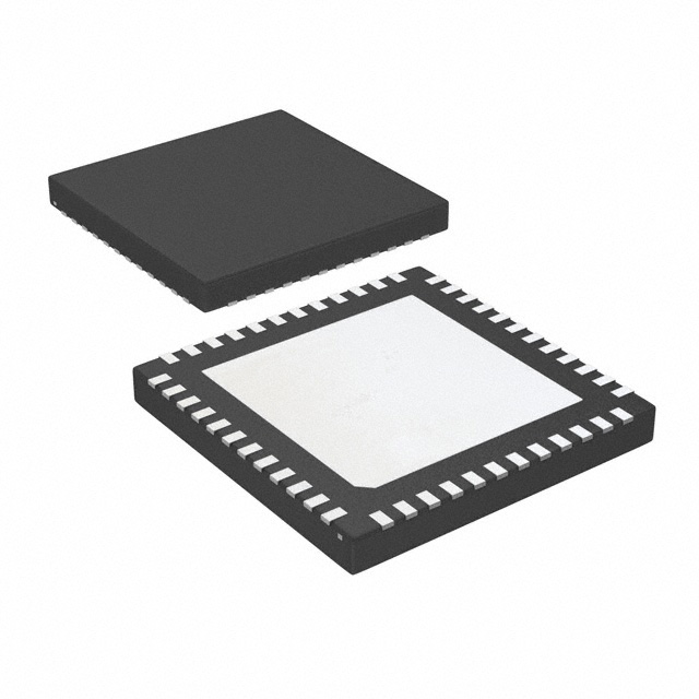
ICGOO电子元器件商城为您提供DS90UB904QSQE/NOPB由Texas Instruments设计生产,在icgoo商城现货销售,并且可以通过原厂、代理商等渠道进行代购。 DS90UB904QSQE/NOPB价格参考¥33.01-¥61.33。Texas InstrumentsDS90UB904QSQE/NOPB封装/规格:接口 - 串行器,解串行器, 900Mbps Deserializer 1 Input 21 Output 48-WQFN (7x7)。您可以下载DS90UB904QSQE/NOPB参考资料、Datasheet数据手册功能说明书,资料中有DS90UB904QSQE/NOPB 详细功能的应用电路图电压和使用方法及教程。
| 参数 | 数值 |
| 产品目录 | 集成电路 (IC)半导体 |
| 描述 | IC SER/DESER 10-43MHZ 18B 48-LLP显示接口集成电路 10-43MHz 18B Color FPD-Link III Dserlzr |
| 产品分类 | |
| 品牌 | Texas Instruments |
| 产品手册 | http://www.ti.com/lit/gpn/ds90ub904q-q1 |
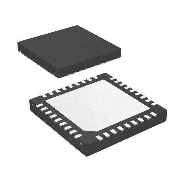
| 产品图片 |
|
| rohs | 符合RoHS无铅 / 符合限制有害物质指令(RoHS)规范要求 |
| 产品系列 | 接口 IC,显示接口集成电路,Texas Instruments DS90UB904QSQE/NOPB- |
| 数据手册 | |
| 产品型号 | DS90UB904QSQE/NOPB |
| 产品培训模块 | http://www.digikey.cn/PTM/IndividualPTM.page?site=cn&lang=zhs&ptm=30144 |
| 产品种类 | 显示接口集成电路 |
| 供应商器件封装 | 48-WQFN(7X7) |
| 其它名称 | *DS90UB904QSQE/NOPB |
| 制造商产品页 | http://www.ti.com/general/docs/suppproductinfo.tsp?distId=10&orderablePartNumber=DS90UB904QSQE/NOPB |
| 功能 | 解串器 |
| 包装 | 剪切带 (CT) |
| 商标 | Texas Instruments |
| 安装类型 | 表面贴装 |
| 安装风格 | SMD/SMT |
| 封装 | Reel |
| 封装/外壳 | 48-WFQFN 裸露焊盘 |
| 封装/箱体 | WQFN-48 |
| 工作温度 | -40°C ~ 105°C |
| 工作温度范围 | - 40 C to + 105 C |
| 工作电源电压 | 1.71 V to 1.89 V |
| 工厂包装数量 | 250 |
| 接口 | I2C |
| 描述/功能 | 18 Bit Color FPD-Link III Deserializer with Bidirectional Control Channel |
| 数据速率 | 900Mbps |
| 最大速度MHz | 43 MHz |
| 标准包装 | 1 |
| 电压-电源 | 1.71 V ~ 1.89 V,3 V ~ 3.6 V |
| 类型 | Display Interface IC |
| 系列 | DS90UB904Q-Q1 |
| 输入数 | 1 |
| 输入类型 | CML |
| 输出数 | 1 |
| 输出类型 | LVCMOS |


- 商务部:美国ITC正式对集成电路等产品启动337调查
- 曝三星4nm工艺存在良率问题 高通将骁龙8 Gen1或转产台积电
- 太阳诱电将投资9.5亿元在常州建新厂生产MLCC 预计2023年完工
- 英特尔发布欧洲新工厂建设计划 深化IDM 2.0 战略
- 台积电先进制程称霸业界 有大客户加持明年业绩稳了
- 达到5530亿美元!SIA预计今年全球半导体销售额将创下新高
- 英特尔拟将自动驾驶子公司Mobileye上市 估值或超500亿美元
- 三星加码芯片和SET,合并消费电子和移动部门,撤换高东真等 CEO
- 三星电子宣布重大人事变动 还合并消费电子和移动部门
- 海关总署:前11个月进口集成电路产品价值2.52万亿元 增长14.8%


PDF Datasheet 数据手册内容提取
DS90UB903Q, DS90UB904Q www.ti.com SNLS332E–JUNE2010–REVISEDAPRIL2013 DS90UB903Q/DS90UB904Q 10 - 43MHz 18 Bit Color FPD-Link III Serializer and Deserializer with Bidirectional Control Channel CheckforSamples:DS90UB903Q,DS90UB904Q FEATURES DESCRIPTION 1 • 10MHzto43MHzInputPCLKSupport The DS90UB903Q/DS90UB904Q chipset offers a 2 FPD-Link III interface with a high-speed forward • 210Mbpsto903MbpsDataThroughput channel and a bidirectional control channel for data • SingleDifferentialPairInterconnect transmission over a single differential pair. The • BidirectionalControlInterfaceChannelwith DS90UB903Q/904Q incorporates differential I2CSupport signalingonboththehigh-speedforwardchanneland bidirectional control channel data paths. The • EmbeddedClockwithDCBalancedCodingto Serializer/ Deserializer pair is targeted for direct SupportAC-CoupledInterconnects connections between graphics host controller and • CapabletoDriveupto10MetersShielded displays modules. This chipset is ideally suited for Twisted-Pair driving video data to displays requiring 18-bit color • I2CCompatibleSerialInterface depth (RGB666 + HS, VS, and DE) along with bidirectional control channel bus. The primary • SingleHardwareDeviceAddressingPin transport converts 21 bit data over a single high- • Upto4GeneralPurposeInput(GPI)/Output speed serial stream, along with a separate low (GPO) latency bidirectional control channel transport that accepts control information from an I2C port. Using • LOCKOutputReportingPinandAT-SPEED TI’s embedded clock technology allows transparent BISTDiagnosisFeaturetoValidateLink full-duplex communication over a single differential Integrity pair, carrying asymmetrical bidirectional control • IntegratedTerminationResistors channel information in both directions. This single • 1.8V-or3.3V-CompatibleParallelBusInterface serial stream simplifies transferring a wide data bus over PCB traces and cable by eliminating the skew • SinglePowerSupplyat1.8V problems between parallel data and clock paths. This • ISO10605ESDandIEC61000-4-2ESD significantly saves system cost by narrowing data Compliant paths that in turn reduce PCB layers, cable width, • AutomotiveGradeProduct:AEC-Q100Grade2 andconnectorsizeandpins. Qualified In addition, the Deserializer inputs provide • TemperatureRange−40°Cto+105°C equalization control to compensate for loss from the media over longer distances. Internal DC balanced • NoReferenceClockRequiredonDeserializer encoding/decoding is used to support AC-Coupled • ProgrammableReceiveEqualization interconnects. • EMI/EMCMitigation The Serializer is offered in a 40-pin lead in WQFN – DESProgrammableSpreadSpectrum and Deserializer is offered in a 48-pin WQFN (SSCG)Outputs packages. – DESReceiverStaggeredOutputs APPLICATIONS • AutomotiveDisplaySystems – CentralInformationDisplays – NavigationDisplays – RearSeatEntertainment – TouchScreenDisplays 1 Pleasebeawarethatanimportantnoticeconcerningavailability,standardwarranty,anduseincriticalapplicationsof TexasInstrumentssemiconductorproductsanddisclaimerstheretoappearsattheendofthisdatasheet. Alltrademarksarethepropertyoftheirrespectiveowners. 2 PRODUCTIONDATAinformationiscurrentasofpublicationdate. Copyright©2010–2013,TexasInstrumentsIncorporated Products conform to specifications per the terms of the Texas Instruments standard warranty. Production processing does not necessarilyincludetestingofallparameters.
DS90UB903Q, DS90UB904Q SNLS332E–JUNE2010–REVISEDAPRIL2013 www.ti.com Typical Application Diagram Parallel FPD-Link III Parallel Data In Data Out 18+3 18+3 Graphics Controller 4 4 Display -- DS90UB903Q DS90UB904Q Module, Video GPO GPI Touch Panel Bidirectional Processor 2 2 Control Channel Bidirectional Bidirectional Control Bus Serializer Deserializer Control Bus Figure1. TypicalApplicationCircuit Block Diagrams RH/GSGP,/VBOS[[5,3D::00E]], 241 Input Latch Encoder Serializer RT RT DOUT+ RIN+ RT RT Deserializer Decoder Output Latch 241RHG/SPG,IV[/3BS:[05,D]:0E], DOUT- RIN- PCLK PCLK PLL CGloecnk CDR Clock LOCK Gen PASS PDB Timing PDB and Timing MODE Control BISTEN and MODE Control re re d d ISSDDC[xAL] I2C Controller OFIF redooccenE redooccneD OFIF I2C Controller ISSDDC[xAL] D E DS90UB903Q - SERIALIZER DS90UB904Q - DESERIALIZER Figure2. BlockDiagram DS90UB903Q DS90UB904Q Serializer Deserializer R[5:0] FPD-Link III R[5:0] G[5:0] G[5:0] B[5:0] B[5:0] Timing VS VS Controller HS HS DE DE Graphics PCLK Controller --- Video PCLK PLL LCD PDB Display Processor MOPDDEB Config. Config. MBGIPOSIDT[3EE:0N] Touch-- -Panel GPO[3:0] PC SSDCAL I2C I2C SSDCAL PC Figure3. ApplicationBlockDiagram 2 SubmitDocumentationFeedback Copyright©2010–2013,TexasInstrumentsIncorporated ProductFolderLinks:DS90UB903Q DS90UB904Q
DS90UB903Q, DS90UB904Q www.ti.com SNLS332E–JUNE2010–REVISEDAPRIL2013 DS90UB903Q Pin Diagram DIN[7] DIN[6] DIN[5] DIN[4] DIN[3] DIN[2] DIN[1] DIN[0] GPO[3] GPO[2] 0 9 8 7 6 5 4 3 2 1 3 2 2 2 2 2 2 2 2 2 VDDIO 31 20 GPO[1] DIN[8] 32 DAP = GND 19 GPO[0] DIN[9] 33 18 VDDCML VDDD 34 17 DOUT+ DS9UB903Q DIN[10] 35 16 DOUT- Serializer 40-Pin WQFN DIN[11] 36 (Top View) 15 VDDT DIN[12] 37 14 VDDPLL DIN[13] 38 13 PDB DIN[14] 39 12 MODE DIN[15] 40 11 RES 1 2 3 4 5 6 7 8 9 10 DIN[16] DIN[17] DIN[18] DIN[19] DIN[20] PCLK SCL SDA ID[x] RES Serializer-DS90UB903Q 40PinWQFN(TopView) SeePackageNumberRTA0040A DS90UB903QSERIALIZERPINDESCRIPTIONS PinName PinNo. I/O,Type Description LVCMOSPARALLELINTERFACE DIN[20:0] 5,4,3,2,1, Inputs, Paralleldatainputs. 40,39,38,37, LVCMOS 36,35,33,32, w/pulldown 30,29,28,27, 26,25,24,23 PCLK 6 Input,LVCMOS PixelClockInputPin.StrobeedgesetbyTRFBcontrolregister. w/pulldown GENERALPURPOSEOUTPUT(GPO) GPO[3:0] 22,21,20,19 Output, General-purposeoutputpinscanbeusedtocontrolandrespondtovarious LVCMOS commands. BIDIRECTIONALCONTROLBUS-I2CCOMPATIBLE Input/Output, Clocklineforthebidirectionalcontrolbuscommunication SCL 7 OpenDrain SCLrequiresanexternalpull-upresistortoV . DDIO Input/Output, Datalineforthebidirectionalcontrolbuscommunication SDA 8 OpenDrain SDArequiresanexternalpull-upresistortoV . DDIO I2CModeselect MODE=L,Mastermode(default);DevicegeneratesanddrivestheSCLclockline. Deviceisconnectedtoslaveperipheralonthebus.(Serializerinitiallystartsupin Input,LVCMOS MODE 12 StandbymodeandisenabledthroughremotewakeupbyDeserializer) w/pulldown MODE=H,Slavemode;DeviceacceptsSCLclockinputandattachedtoanI2C controllermasteronthebus.SlavemodedoesnotgeneratetheSCLclock,butuses theclockgeneratedbytheMasterforthedatatransfers. DeviceIDAddressSelect ID[x] 9 Input,analog ResistortoGroundand10kΩpull-upto1.8Vrail.SeeTable3 CONTROLANDCONFIGURATION Copyright©2010–2013,TexasInstrumentsIncorporated SubmitDocumentationFeedback 3 ProductFolderLinks:DS90UB903Q DS90UB904Q
DS90UB903Q, DS90UB904Q SNLS332E–JUNE2010–REVISEDAPRIL2013 www.ti.com DS90UB903QSERIALIZERPINDESCRIPTIONS(continued) PinName PinNo. I/O,Type Description PowerdownModeInputPin. PDB=H,SerializerisenabledandisON. Input,LVCMOS PDB 13 PDB=L,SerailizerisinPowerDownmode.WhentheSerializerisinPowerDown, w/pulldown thePLLisshutdown,andIDDisminimized.Programmedcontrolregisterdataare NOTretainedandresettodefaultvalues Input,LVCMOS Reserved. RES 10,11 w/pulldown ThispinMUSTbetiedLOW. FPD-LINKIIIINTERFACE Input/Output, Non-invertingdifferentialoutput,bidirectionalcontrolchannelinput.Theinterconnect DOUT+ 17 CML mustbeACCoupledwitha100nFcapacitor. DOUT- 16 Input/Output, Invertingdifferentialoutput,bidirectionalcontrolchannelinput.Theinterconnectmust CML beACCoupledwitha100nFcapacitor. POWERANDGROUND VDDPLL 14 Power,Analog PLLPower,1.8V±5% VDDT 15 Power,Analog TxAnalogPower,1.8V±5% VDDCML 18 Power,Analog CML&BidirectionalChannelDriverPower,1.8V±5% VDDD 34 Power,Digital DigitalPower,1.8V±5% Power,Digital PowerforI/Ostage.Thesingle-endedinputsandSDA,SCLarepoweredfromV . VDDIO 31 DDIO V canbeconnectedtoa1.8V±5%or3.3V±10% DDIO Ground,DAP DAPmustbegrounded.DAPisthelargemetalcontactatthebottomside,locatedat VSS DAP thecenteroftheWQFNpackage.Connectedtothegroundplane(GND)withatleast 16vias. 4 SubmitDocumentationFeedback Copyright©2010–2013,TexasInstrumentsIncorporated ProductFolderLinks:DS90UB903Q DS90UB904Q
DS90UB903Q, DS90UB904Q www.ti.com SNLS332E–JUNE2010–REVISEDAPRIL2013 DS90UB904Q Pin Diagram DDR DB OCK PI[0] PI[1] PI[2] PI[3] DDIO1 OUT[0] OUT[1] OUT[2] OUT[3] V P L G G G G V R R R R 6 5 4 3 2 1 0 9 8 7 6 5 3 3 3 3 3 3 3 2 2 2 2 2 PASS 37 24 ROUT[4] RES/CMLOUTP 38 DAP = GND 23 ROUT[5] RES/CMLOUTN 39 22 ROUT[6] VDDCML 40 21 ROUT[7] RIN+ 41 20 VDDIO2 DS90UB904Q RIN- 42 Deserializer 19 ROUT[8] 48-Pin WQFN RES 43 18 ROUT[9] (Top View) BISTEN 44 17 VDDD VDDPLL 45 16 ROUT[10] RES 46 15 ROUT[11] MODE 47 14 ROUT[12] ID[x] 48 13 ROUT[13] 1 2 3 4 5 6 7 8 9 10 11 12 SDA SCL DDSSCG PCLK OUT[20] OUT[19] VDDIO3 OUT[18] OUT[17] OUT[16] OUT[15] OUT[14] V R R R R R R R Deserializer-DS90UB904Q 48PinWQFN(TopView) SeePackageNumberRHS0048A DS90UB904QDESERIALIZERPINDESCRIPTIONS PinName PinNo. I/O,Type Description LVCMOSPARALLELINTERFACE ROUT[20:0] 5,6,8,9,10, Outputs, Paralleldataoutputs. 11,12,13,14, LVCMOS 15,16,18,19, 21,22,23,24, 25,26,27,28 Output, PixelClockOutputPin. PCLK 4 LVCMOS StrobeedgesetbyRRFBcontrolregister. GENERALPURPOSEINPUT(GPI) General-purposeinputpinscanbeusedtocontrolandrespondtovarious GPI[3:0] 30,31,32,33 Input,LVCMOS commands. BIDIRECTIONALCONTROLBUS-I2CCOMPATIBLE Input/Output, Clocklineforthebidirectionalcontrolbuscommunication SCL 2 OpenDrain SCLrequiresanexternalpull-upresistortoV . DDIO Input/Output, Datalineforbidirectionalcontrolbuscommunication SDA 1 OpenDrain SDArequiresanexternalpull-upresistortoV . DDIO I2CModeselect MODE=L,Mastermode;DevicegeneratesanddrivestheSCLclockline,where Input,LVCMOS requiredsuchasRead.Deviceisconnectedtoslaveperipheralonthebus. MODE 47 w/pullup MODE=H,Slavemode(default);DeviceacceptsSCLclockinputandattachedtoan I2Ccontrollermasteronthebus.SlavemodedoesnotgeneratetheSCLclock,but usestheclockgeneratedbytheMasterforthedatatransfers. DeviceIDAddressSelect ID[x] 48 Input,analog ResistortoGroundand10kΩpull-upto1.8Vrail.SeeTable4. CONTROLANDCONFIGURATION Copyright©2010–2013,TexasInstrumentsIncorporated SubmitDocumentationFeedback 5 ProductFolderLinks:DS90UB903Q DS90UB904Q
DS90UB903Q, DS90UB904Q SNLS332E–JUNE2010–REVISEDAPRIL2013 www.ti.com DS90UB904QDESERIALIZERPINDESCRIPTIONS(continued) PinName PinNo. I/O,Type Description PowerdownModeInputPin. PDB=H,DeserializerisenabledandisON. Input,LVCMOS PDB 35 PDB=L,DeserializerisinPowerDownmode.WhentheDeserializerisinPower w/pulldown Down.ProgrammedcontrolregisterdataareNOTretainedandresettodefault values. LOCKStatusOutputPin. Output, LOCK=H,PLLisLocked,outputsareactive LOCK 34 LVCMOS LOCK=L,PLLisunlocked,ROUTandPCLKoutputstatesarecontrolledby OSS_SELcontrolregister.MaybeusedasLinkStatus. Reserved. Pins38,39:Routetotestpointorleaveopenifunused.SeealsoFPD-LINKIII RES 38,39,43,46 - INTERFACEpindescriptionsection. Pin46:ThispinMUSTbetiedLOW. Pin43:Leavepinopen. BISTMODE BISTEnablePin. Input,LVCMOS BISTEN 44 BISTEN=H,BISTModeisenabled. w/pulldown BISTEN=L,BISTModeisdisabled. PASSOutputPinforBISTmode. Output, PASS=H,ERRORFREETransmission PASS 37 LVCOMS PASS=L,oneormoreerrorsweredetectedinthereceivedpayload. LeaveOpenifunused.Routetotestpoint(pad)recommended. FPD-LINKIIIINTERFACE Input/Output, Non-invertingdifferentialinput,bidirectionalcontrolchanneloutput.Theinterconnect RIN+ 41 CML mustbeACCoupledwitha100nFcapacitor. Input/Output, Invertingdifferentialinput,bidirectionalcontrolchanneloutput.Theinterconnectmust RIN- 42 CML beACCoupledwitha100nFcapacitor. Non-invertingCMLOutput CMLOUTP 38 Output,CML Monitorpointforequalizeddifferentialsignal.Testportisenabledviacontrol registers. InvertingCMLOutput CMLOUTN 39 Output,CML Monitorpointforequalizeddifferentialsignal.Testportisenabledviacontrol registers. POWERANDGROUND SSCGPower,1.8V±5% VDDSSCG 3 Power,Digital PowersupplymustbeconnectedregardlessifSSCGfunctionisinoperation. LVCMOSI/OBufferPower,Thesingle-endedoutputsandcontrolinputarepowered VDDIO1/2/3 29,20,7 Power,Digital fromV .V canbeconnectedtoa1.8V±5%or3.3V±10% DDIO DDIO VDDD 17 Power,Digital DigitalCorePower,1.8V±5% VDDR 36 Power,Analog RxAnalogPower,1.8V±5% VDDCML 40 Power,Analog BidirectionalChannelDriverPower,1.8V±5% VDDPLL 45 Power,Analog PLLPower,1.8V±5% DAPmustbegrounded.DAPisthelargemetalcontactatthebottomside,locatedat VSS DAP Ground,DAP thecenteroftheWQFNpackage.Connectedtothegroundplane(GND)withatleast 16vias. Thesedeviceshavelimitedbuilt-inESDprotection.Theleadsshouldbeshortedtogetherorthedeviceplacedinconductivefoam duringstorageorhandlingtopreventelectrostaticdamagetotheMOSgates. 6 SubmitDocumentationFeedback Copyright©2010–2013,TexasInstrumentsIncorporated ProductFolderLinks:DS90UB903Q DS90UB904Q
DS90UB903Q, DS90UB904Q www.ti.com SNLS332E–JUNE2010–REVISEDAPRIL2013 Absolute Maximum Ratings(1)(2)(3) SupplyVoltage–V (1.8V) −0.3Vto+2.5V DDn SupplyVoltage–V −0.3Vto+4.0V DDIO LVCMOSInputVoltageI/OVoltage −0.3Vto+(VDDIO+0.3V) CMLDriverI/OVoltage(V ) −0.3Vto+(V +0.3V) DD DD CMLReceiverI/OVoltage(V ) −0.3Vto(V +0.3V) DD DD JunctionTemperature +150°C StorageTemperature −65°Cto+150°C MaximumPackagePowerDissipationCapacity 1/θ °C/Wabove+25° JA PackageDerating θ (basedon16thermalvias) 30.7°C/W JA 40LeadWQFN θ (basedon16thermalvias) 6.8°C/W JC θ (basedon16thermalvias) 26.9°C/W JA 48LeadWQFN θ (basedon16thermalvias) 4.4°C/W JC ESDRating(IEC61000-4-2) R =330Ω,C =150pF D S AirDischarge(DOUT+,DOUT-,RIN+,RIN-) ≥±25kV ContactDischarge(DOUT+,DOUT-,RIN+,RIN-) ≥±10kV ESDRating(ISO10605) R =330Ω,C =150/330pF D S ESDRating(ISO10605) R =2KΩ,C =150/330pF D S AirDischarge(DOUT+,DOUT-,RIN+,RIN-) ≥±15kV ContactDischarge(DOUT+,DOUT-,RIN+,RIN-) ≥±10kV ESDRating(HBM) ≥±8kV ESDRating(CDM) ≥±1kV ESDRating(MM) ≥±250V (1) “AbsoluteMaximumRatings”indicatelimitsbeyondwhichdamagetothedevicemayoccur,includinginoperabilityanddegradationof devicereliabilityand/orperformance.Functionaloperationofthedeviceand/ornon-degradationattheAbsoluteMaximumRatingsor otherconditionsbeyondthoseindicatedintheRecommendedOperatingConditionsisnotimplied.TheRecommendedOperating Conditionsindicateconditionsatwhichthedeviceisfunctional;thedeviceshouldnotbeoperatedbeyondsuchconditions. (2) Forsolderingspecifications:seeproductfolderatwww.ti.com (3) IfMilitary/Aerospacespecifieddevicesarerequired,pleasecontacttheTexasInstrumentsSalesOffice/Distributorsforavailabilityand specifications. Recommended Operating Conditions(1) Min Nom Max Units SupplyVoltage(V ) 1.71 1.8 1.89 V DDn LVCMOSSupplyVoltage(V ) 1.71 1.8 1.89 V DDIO OR LVCMOSSupplyVoltage(V ) 3.0 3.3 3.6 V DDIO V (1.8V) 25 mVp-p DDn SupplyNoise V (1.8V) 25 mVp-p DDIO V (3.3V) 50 mVp-p DDIO OperatingFreeAirTemperature(T ) -40 +25 +105 °C A PCLKClockFrequency 10 43 MHz (1) Supplynoisetestingwasdonewithminimumcapacitors(asshownonFigure37andFigure38)onthePCB.AsinusoidalsignalisAC coupledtotheVDDn(1.8V)supplywithamplitude=25mVp-pmeasuredatthedeviceVDDnpins.Biterrorratetestingofinputtothe SerandoutputoftheDeswith10metercableshowsnoerrorwhenthenoisefrequencyontheSerislessthan1MHz.TheDesonthe otherhandshowsnoerrorwhenthenoisefrequencyislessthan750kHz. Copyright©2010–2013,TexasInstrumentsIncorporated SubmitDocumentationFeedback 7 ProductFolderLinks:DS90UB903Q DS90UB904Q
DS90UB903Q, DS90UB904Q SNLS332E–JUNE2010–REVISEDAPRIL2013 www.ti.com Electrical Characteristics(1)(2)(3) Overrecommendedoperatingsupplyandtemperaturerangesunlessotherwisespecified. Symbol Parameter Conditions Min Typ Max Units LVCMOSDCSPECIFICATIONS3.3VI/O(SERINPUTS,DESOUTPUTS,GPI,GPO,CONTROLINPUTSANDOUTPUTS) V HighLevelInput IH V =3.0Vto3.6V 2.0 V V Voltage IN IN V LowLevelInput IL V =3.0Vto3.6V GND 0.8 V Voltage IN I InputCurrent V =0Vor3.6V,V =3.0Vto3.6V -20 ±1 +20 µA IN IN IN V HighLevelOutput OH V =3.0Vto3.6V,I =−4mA 2.4 V V Voltage DDIO OH DDIO V LowLevelOutput OL V =3.0Vto3.6V,I =+4mA GND 0.4 V Voltage DDIO OL I SerializerGPO OS -24 OutputShortCircuit Outputs V =0V mA Current OUT DeserializerLVCMOS -39 Outputs TRI-STATEOutput PDB=0V, I LVCMOSOutputs -20 ±1 +20 µA OZ Current V =0VorV OUT DD LVCMOSDCSPECIFICATIONS1.8VI/O(SERINPUTS,DESOUTPUTS,GPI,GPO,CONTROLINPUTSANDOUTPUTS) V HighLevelInput IH V =1.71Vto1.89V 0.65V V +0.3 Voltage IN IN IN V V LowLevelInput IL V =1.71Vto1.89V GND 0.35V Voltage IN IN I InputCurrent V =0Vor1.89V,V =1.71Vto1.89V -20 ±1 +20 µA IN IN IN V HighLevelOutput V - OH V =1.71Vto1.89V,I =−4mA DDIO V V Voltage DDIO OH 0.45 DDIO V LowLevelOutput V =1.71Vto1.89V DeserializerLVCMOS OL DDIO GND 0.45 V Voltage I =+4mA Outputs OL I SerializerGPO OS -11 OutputShortCircuit Outputs V =0V mA Current OUT DeserializerLVCMOS -20 Outputs I TRI-STATEOutput PDB=0V, OZ LVCMOSOutputs -20 ±1 +20 µA Current V =0VorV OUT DD CMLDRIVERDCSPECIFICATIONS(DOUT+,DOUT-) OutputDifferential |V | R =100Ω(Figure8) 268 340 412 mV OD Voltage T OutputDifferential ΔV R =100Ω 1 50 mV OD VoltageUnbalance L V OutputDifferential V - V - OS R =100Ω(Figure8) DD(MIN) V -V DD(MAX) V OffsetVoltage L V DD OD V OD(MAX) OD(MIN) ΔV OffsetVoltage OS R =100Ω 1 50 mV Unbalance L I OutputShortCircuit OS DOUT+/-=0V -27 mA Current R DifferentialInternal T Termination DifferentialacrossDOUT+andDOUT- 80 100 120 Ω Resistance CMLRECEIVERDCSPECIFICATIONS(RIN+,RIN-) (1) TheElectricalCharacteristicstableslistensuredspecificationsunderthelistedRecommendedOperatingConditionsexceptas otherwisemodifiedorspecifiedbytheElectricalCharacteristicsConditionsand/orNotes.Typicalspecificationsareestimationsonlyand arenotensured. (2) Currentintodevicepinsisdefinedaspositive.Currentoutofadevicepinisdefinedasnegative.Voltagesarereferencedtoground exceptVOD,ΔVOD,VTHandVTLwhicharedifferentialvoltages. (3) Typicalvaluesrepresentmostlikelyparametricnormsat1.8Vor3.3V,T =+25°C,andattheRecommendedOperationConditionsat A thetimeofproductcharacterizationandarenotensured. 8 SubmitDocumentationFeedback Copyright©2010–2013,TexasInstrumentsIncorporated ProductFolderLinks:DS90UB903Q DS90UB904Q
DS90UB903Q, DS90UB904Q www.ti.com SNLS332E–JUNE2010–REVISEDAPRIL2013 Electrical Characteristics(1)(2)(3) (continued) Overrecommendedoperatingsupplyandtemperaturerangesunlessotherwisespecified. Symbol Parameter Conditions Min Typ Max Units DifferentialThreshold V +90 TH HighVoltage (Figure10) mV V DifferentialThreshold TL -90 LowVoltage V DifferentialInput IN RIN+-RIN- 180 mV VoltageRange I InputCurrent V =V or0V,V =1.89V -20 ±1 +20 µA IN IN DD DD R DifferentialInternal T Termination DifferentialacrossRIN+andRIN- 80 100 120 Ω Resistance SER/DESSUPPLYCURRENT*DIGITAL,PLL,ANDANALOGVDD I R =100Ω DDT T Serializer(Tx) WORSTCASEpattern VDDn=1.89V 62 90 VDDnSupplyCurrent (Figure5) PCLK=43MHz mA (includesload current) RT=100Ω DefaultRegisters 55 RANDOMPRBS-7pattern I VDDIO=1.89V DDIOT Serializer(Tx) PCLK=43MHz 2 5 VDDIOSupply RT=100Ω DefaultRegisters WORSTCASEpattern mA Current(includesload (Figure5) VDDIO=3.6V current) PCLK=43MHz 7 15 DefaultRegisters I V =1.89V 370 775 DDTZ DDn Serializer(Tx)Supply PDB=0V;Allother I V =1.89V 55 125 µA DDIOTZ CurrentPower-down LVCMOSInputs=0V DDIO V =3.6V 65 135 DDIO I V =1.89V,C =8pF PCLK=43MHz DDR DDn L Deserializer(Rx) WORSTCASEPattern SSCG[3:0]=ON 60 96 VDDnSupplyCurrent (Figure5) DefaultRegisters (includesload current) VDDn=1.89V,CL=8pF PCLK=43MHz 53 RANDOMPRBS-7Pattern DefaultRegisters mA I V =1.89V,C =8pF DDIOR Deserializer(Rx) WDODRIOSTCASEPLattern PCLK=43MHz 21 32 VDDIOSupply (Figure5) DefaultRegisters Current(includesload current) VDDIO=3.6V,CL=8pF PCLK=43MHz 49 83 WORSTCASEPattern DefaultRegisters I V =1.89V 42 400 DDRZ Deserializer(Rx) DDn PDB=0V;Allother I SupplyCurrent V =1.89V 8 40 µA DDIORZ LVCMOSInputs=0V DDIO Power-down V =3.6V 350 800 DDIO Recommended Serializer Timing for PCLK(1) Overrecommendedoperatingsupplyandtemperaturerangesunlessotherwisespecified. Symbol Parameter Conditions Min Typ Max Units t TransmitClockPeriod 23.3 T 100 ns TCP t TransmitClockInputHigh TCIH 0.4T 0.5T 0.6T ns Time t TransmitClockInputLow 10MHz–43MHz TCIL 0.4T 0.5T 0.6T ns Time t PCLKInputTransitionTime CLKT 0.5 3 ns (Figure11) f Internaloscillatorclock OSC 25 MHz source (1) RecommendedInputTimingRequirementsareinputspecificationsandnottestedinproduction. Copyright©2010–2013,TexasInstrumentsIncorporated SubmitDocumentationFeedback 9 ProductFolderLinks:DS90UB903Q DS90UB904Q
DS90UB903Q, DS90UB904Q SNLS332E–JUNE2010–REVISEDAPRIL2013 www.ti.com Serializer Switching Characteristics Overrecommendedoperatingsupplyandtemperaturerangesunlessotherwisespecified. Symbol Parameter Conditions Min Typ Max Units t CMLLow-to-HighTransition LHT R =100Ω(Figure6) 150 330 ps Time L t CMLHigh-to-LowTransition HLT R =100Ω(Figure6) 150 330 ps Time L t DataInputSetuptoPCLK 2.0 ns DIS SerializerDataInputs(Figure12) t DataInputHoldfromPCLK 2.0 ns DIH t SerializerPLLLockTime R =100Ω(1)(2) 1 2 ms PLD L t R =100Ω,PCLK=10–43MHz SD T 6.386T 6.386T 6.386T SerializerDelay Register0x03hb[0](TRFB=1) ns +5 +12 +19.7 (Figure14) t Serializeroutputintrinsicdeterministic JIND SerializerOutput jitter.Measured(cycle-cycle)with 0.13 UI DeterministicJitter PRBS-7testpattern PCLK=43MHz(3)(4) t Serializeroutputintrinsicrandomjitter JINR SerializerOutputRandom (cycle-cycle).Alternating-1,0pattern. 0.04 UI Jitter PCLK=43MHz(3)(4) t Serializeroutputpeak-to-peakjitter JINT includesdeterministicjitter,random Peak-to-peakSerializer jitter,andjittertransferfromserializer 0.396 UI OutputJitter input.Measured(cycle-cycle)with PRBS-7testpattern. PCLK=43MHz(3)(4) λ SerializerJitterTransfer PCLK=43MHz,DefaultRegisters STXBW Function-3dBBandwidth (Figure20)(3) 1.90 MHz δ SerializerJitterTransfer PCLK=43MHz,DefaultRegisters STX Function(Peaking) (Figure20)(3) 0.944 dB δ SerializerJitterTransfer STXf PCLK=43MHz,DefaultRegisters Function(Peaking (Figure20)(3) 500 kHz Frequency) (1) t andt isthetimerequiredbytheserializeranddeserializertoobtainlockwhenexitingpower-downstatewithanactivePCLK PLD DDLT (2) Specificationisensuredbydesign. (3) Typicalvaluesrepresentmostlikelyparametricnormsat1.8Vor3.3V,T =+25°C,andattheRecommendedOperationConditionsat A thetimeofproductcharacterizationandarenotensured. (4) UI–UnitIntervalisequivalenttooneidealserializeddatabitwidth.TheUIscaleswithPCLKfrequency. Deserializer Switching Characteristics Overrecommendedoperatingsupplyandtemperaturerangesunlessotherwisespecified. Symbol Parameter Conditions Pin/Freq. Min Typ Max Units t ReceiverOutputClockPeriod t =t PCLK 23.3 T 100 ns RCP RCP TCP t DefaultRegisters PDC PCLKDutyCycle PCLK 45 50 55 % SSCG[3:0]=OFF LVCMOSLow-to-HighTransition V :1.71Vto1.89Vor t DDIO 1.3 2.0 2.8 CLH Time 3.0to3.6V, C =8pF(lumpedload) PCLK ns tCHL LVCMOSHigh-to-LowTransition DLefaultRegisters 1.3 2.0 2.8 Time (Figure16)(1) LVCMOSLow-to-HighTransition V :1.71Vto1.89Vor t DDIO 1.6 2.4 3.3 CLH Time 3.0to3.6V, DeserializerROUTn C =8pF(lumpedload) ns tCHL LVCMOSHigh-to-LowTransition DLefaultRegisters DataOutputs 1.6 2.4 3.3 Time (Figure16)(1) t ROUTSetupDatatoPCLK V :1.71Vto1.89Vor 0.38T 0.5T ROS DDIO 3.0Vto3.6V, DeserializerROUTn tROH ROUTHoldDatatoPCLK CL=8pF(lumpedload) DataOutputs 0.38T 0.5T ns DefaultRegisters (1) Specificationisensuredbycharacterizationandisnottestedinproduction. 10 SubmitDocumentationFeedback Copyright©2010–2013,TexasInstrumentsIncorporated ProductFolderLinks:DS90UB903Q DS90UB904Q
DS90UB903Q, DS90UB904Q www.ti.com SNLS332E–JUNE2010–REVISEDAPRIL2013 Deserializer Switching Characteristics (continued) Overrecommendedoperatingsupplyandtemperaturerangesunlessotherwisespecified. Symbol Parameter Conditions Pin/Freq. Min Typ Max Units DefaultRegisters 4.571T 4.571T 4.571T t DeserializerDelay Register0x03hb[0] 10MHz–43MHz ns DD +8 +12 +16 (RRFB=1)(Figure17) t DeserializerDataLockTime (Figure15)(2) 10MHz–43MHz 10 ms DDLT t (Figure19, RJIT ReceiverInputJitterTolerance Figure21)(3)(4) 43MHz 0.53 UI tRCJ PCLK 10MHz 300 550 ReceiverClockJitter SSCG[3:0]=OFF(1)(5) 43MHz 120 250 ps tDPJ PCLK 10MHz 425 600 DeserializerPeriodJitter SSCG[3:0]=OFF(1)(6) 43MHz 320 480 ps tDCCJ DeserializerCycle-to-CycleClock PCLK 10MHz 320 500 Jitter SSCG[3:0]=OFF(1)(7) 43MHz 300 500 ps fdev SpreadSpectrumClocking ±0.5%to DeviationFrequency LVCMOSOutputBus 20MHz–43MHz ±2.0% % SSC[3:0]=ON fmod SpreadSpectrumClocking (Figure22) 20MHz–43MHz 9kHzto kHz ModulationFrequency 66kHz (2) t andt isthetimerequiredbytheserializeranddeserializertoobtainlockwhenexitingpower-downstatewithanactivePCLK PLD DDLT (3) UI–UnitIntervalisequivalenttooneidealserializeddatabitwidth.TheUIscaleswithPCLKfrequency. (4) t max(0.61UI)islimitedbyinstrumentationandactualt ofin-bandjitteratlowfrequency(<2MHz)isgreater1UI. RJIT RJIT (5) t isthemaximumamountofjittermeasuredover30,000samplesbasedonTimeIntervalError(TIE). DCJ (6) t isthemaximumamounttheperiodisallowedtodeviatemeasuredover30,000samples. DPJ (7) t isthemaximumamountofjitterbetweenadjacentclockcyclesmeasuredover30,000samples. DCCJ Copyright©2010–2013,TexasInstrumentsIncorporated SubmitDocumentationFeedback 11 ProductFolderLinks:DS90UB903Q DS90UB904Q
DS90UB903Q, DS90UB904Q SNLS332E–JUNE2010–REVISEDAPRIL2013 www.ti.com Bidirectional Control Bus AC Timing Specifications (SCL, SDA) - I2C Compliant Overrecommendedsupplyandtemperaturerangesunlessotherwisespecified.SeeFigure4. Symbol Parameter Conditions Min Typ Max Units RECOMMENDEDINPUTTIMINGREQUIREMENTS(1) f SCLClockFrequency >0 100 kHz SCL t SCLLowPeriod 4.7 µs LOW t SCLHighPeriod 4.0 µs HIGH Holdtimeforastartorarepeatedstart t 4.0 µs HD:STA condition SetUptimeforastartorarepeated t 4.7 µs SU:STA startcondition tHD:DAT DataHoldTime fSCL=100kHz 0 3.45 µs t DataSetUpTime 250 ns SU:DAT t SetUpTimeforSTOPCondition 4.0 µs SU:STO t SCL&SDARiseTime 1000 ns r t SCL&SDAFallTime 300 ns f C Capacitiveloadforbus 400 pF b SWITCHINGCHARACTERISTICS(2) SerializerMODE=0–R/W 100 Register0x05=0x40'h f SCLClockFrequency kHz SCL DeserializerMODE=0–READ 100 Register0x06b[6:4]=0x00'h SerializerMODE=0–R/W Register0x05=0x40'h t SCLLowPeriod 4.7 µs LOW DeserializerMODE=0–READ Register0x06b[6:4]=0x00'h SerializerMODE=0–R/W Register0x05=0x40'h t SCLHighPeriod 4.0 µs HIGH DeserializerMODE=0–READ Register0x06b[6:4]=0x00'h Holdtimeforastartorarepeatedstart SerializerMODE=0 t 4.0 µs HD:STA condition Register0x05=0x40'h SetUptimeforastartorarepeated SerializerMODE=0 t 4.7 µs SU:STA startcondition Register0x05=0x40'h t DataHoldTime 0 3.45 µs HD:DAT t DataSetUpTime 250 ns SU:DAT t SetUpTimeforSTOPCondition SerializerMODE=0 4.0 µs SU:STO t SCL&SDAFallTime 300 ns f Busfreetimebetweenastopandstart t SerializerMODE=0 4.7 µs BUF condition SerializerMODE=1 1 tTIMEOUT NACKTimeout DeserializerMODE=1 ms 25 Register0x06b[2:0]=111'b (1) RecommendedInputTimingRequirementsareinputspecificationsandnottestedinproduction. (2) Specificationisensuredbydesign. 12 SubmitDocumentationFeedback Copyright©2010–2013,TexasInstrumentsIncorporated ProductFolderLinks:DS90UB903Q DS90UB904Q
DS90UB903Q, DS90UB904Q www.ti.com SNLS332E–JUNE2010–REVISEDAPRIL2013 SDA tBUF tf tLOW tHD;STA tr tr tf SCL tHD;STA tSU;STA tSU;STO tHIGH tHD;DAT tSU;DAT START REPEATED STOP START START Figure4. BidirectionalControlBusTiming Bidirectional Control Bus DC Characteristics (SCL, SDA) - I2C Compliant Overrecommendedsupplyandtemperaturerangesunlessotherwisespecified. Symbol Parameter Conditions Min Typ Max Units V 0.7x IH InputHighLevel SDAandSCL V V V DDIO DDIO V 0.3x IL InputLowLevelVoltage SDAandSCL GND V V DDIO V InputHysteresis SDAandSCL >50 mV HY I TRI-STATEOutputCurrent PDB=0V,V =0VorV -20 ±1 +20 µA OZ OUT DD I InputCurrent SDAorSCL,Vin=V orGND -20 ±1 +20 µA IN DDIO C InputPinCapacitance <5 pF IN V SCLandSDA,V =3.0V OL DDIO 0.36 V I =1.5mA OL LowLevelOutputVoltage SCLandSDA,V =1.71V DDIO 0.36 V I =1mA OL AC Timing Diagrams and Test Circuits Device Pin Name Signal Pattern T PCLK (RFB = H) DIN/ROUT Figure5. “WorstCase”TestPattern 80% 80% Vdiff Vdiff = 0V 20% 20% tLHT tHLT Vdiff = (DOUT+) - (DOUT-) Figure6. SerializerCMLOutputLoadandTransitionTimes Copyright©2010–2013,TexasInstrumentsIncorporated SubmitDocumentationFeedback 13 ProductFolderLinks:DS90UB903Q DS90UB904Q
DS90UB903Q, DS90UB904Q SNLS332E–JUNE2010–REVISEDAPRIL2013 www.ti.com DOUT+ 100 nF 50: SCOPE ZDiff = 100: 100: BW 8 4.0 GHz 50: DOUT- 100 nF Figure7. SerializerCMLOutputLoadandTransitionTimes L A IR ES DOUT+ 21 -O DIN T-L RL E LLA DOUT- R A P PCLK Figure8. SerializerVODDCDiagram Single Ended DOUT- VOD VOD+ VOD- DOUT+ | VOS 0V Differential V OD+ (DOUT+)-(DOUT-) 0V V OD- Figure9. SerializerVODDCDiagram RIN+ RIN+ VTH VCM VID VIN VTL VID VIN RIN- RIN- GND Figure10. DifferentialVTH/VTLDefinitionDiagram 80% 80% VDD PCLK 20% 20% 0V tCLKT tCLKT Figure11. SerializerInputClockTransitionTimes 14 SubmitDocumentationFeedback Copyright©2010–2013,TexasInstrumentsIncorporated ProductFolderLinks:DS90UB903Q DS90UB904Q
DS90UB903Q, DS90UB904Q www.ti.com SNLS332E–JUNE2010–REVISEDAPRIL2013 tTCP PCLK VDDIO/2 VDDIO/2 VDDIO/2 tDIS tDIH VDDIO DINn VDDIO/2 Setup Hold VDDIO/2 0V Figure12. SerializerSetup/HoldTimes PDB VDDIO/2 PCLK tPLD DOUT± TRI-STATE Output Active TRI-STATE Figure13. SerializerDataLockTime | | | | DIN SYMBOL N SYMBOL N+1 SYMBOL N+2 SYMBOL N+3 | | | | tSD VDDIO/2 PCLK | | | | SYMBOL N-4 SYMBOL N-3 SYMBOL N-2 SYMBOL N-1 SYMBOL N | | | | | DOUT+- 0V | | | | | Figure14. SerializerDelay PDB VDDIO/2 tDDLT | RIN± | LOCK TRI-STATE VDDIO/2 | Figure15. DeserializerDataLockTime 80% 80% Deserializer 20% 20% 8 pF lumped tCLH tCHL Figure16. DeserializerLVCMOSOutputLoadandTransitionTimes Copyright©2010–2013,TexasInstrumentsIncorporated SubmitDocumentationFeedback 15 ProductFolderLinks:DS90UB903Q DS90UB904Q
DS90UB903Q, DS90UB904Q SNLS332E–JUNE2010–REVISEDAPRIL2013 www.ti.com SYMBOL N SYMBOL N + 1 SYMBOL N + 2 SYMBOL N + 3 SYMBOL N + 3 | | | | | RIN± 0V | | | | | tDD PCLK VDDIO/2 | | | | | | | | | | ROUTn SYMBOL N - 3 SYMBOL N - 2 SYMBOL N - 1 SYMBOL N SYMBOL N+1 | | | | | Figure17. DeserializerDelay tRCP VDDIO PCLK 1/2 VDDIO 1/2 VDDIO 0V VDDIO ROUT[n], VS, HS 1/2 VDDIO 1/2 VDDIO 0V tROS tROH Figure18. DeserializerOutputSetup/HoldTimes Ideal Data Bit Sampling Ideal Data Beginning Window Bit End VTH 0V RxIN_TOL RxIN_TOL Left Right VTL Ideal Center Position (tBIT/2) tBIT (1 UI) tRJIT = RxIN_TOL (Left + Right) Sampling Window = 1 UI - tRJIT Figure19. ReceiverInputJitterTolerance 2 0 -2 B) R (d -4 E F -6 S N A -8 R R T -10 E T -12 T JI -14 -16 -18 1.0E+04 1.0E+05 1.0E+06 1.0E+07 MODULATION FREQUENCY (Hz) Figure20. TypicalSerializerJitterTransferFunctionCurveat43MHz 16 SubmitDocumentationFeedback Copyright©2010–2013,TexasInstrumentsIncorporated ProductFolderLinks:DS90UB903Q DS90UB904Q
DS90UB903Q, DS90UB904Q www.ti.com SNLS332E–JUNE2010–REVISEDAPRIL2013 0.62 0.61 UI) 0.60 E ( 0.59 D TU 0.58 LI P 0.57 M R A 0.56 E TT 0.55 JI 0.54 0.53 0.52 1.0E+04 1.0E+05 1.0E+06 1.0E+07 JITTER FREQUENCY (Hz) Figure21. TypicalDeserializerInputJitterToleranceCurveat43MHz Frequency FPCLK+ fdev (max) fdev FPCLK FPCLK- fdev (min) Time 1 / fmod Figure22. SpreadSpectrumClockOutputProfile Copyright©2010–2013,TexasInstrumentsIncorporated SubmitDocumentationFeedback 17 ProductFolderLinks:DS90UB903Q DS90UB904Q
DS90UB903Q, DS90UB904Q SNLS332E–JUNE2010–REVISEDAPRIL2013 www.ti.com Table1. DS90UB903QControlRegisters Addr Name Bits Field R/W Default Description (Hex) 7-bitaddressofSerializer;0x58'h 7:1 DEVICEID (1011_000X'b)default 0 I2CDeviceID RW 0xB0'h 0:DeviceIDisfromID[x] 0 SERIDSEL 1:RegisterI2CDeviceIDoverridesID[x] 7:3 RESERVED 0x00'h Reserved Standbymodecontrol.Retainscontrolregisterdata. SupportedonlywhenMODE=0 2 STANDBY RW 0 0:Enabled.Low-currentStandbymodewithwake-up capability.Suspendsallclocksandfunctions. 1 Reset 1:Disabled.Standbyandwake-updisabled DIGITAL 0 1:Resetsthedevicetodefaultregistervalues.Doesnot 1 RESET0 RW selfclear affectdeviceI2CBusorDeviceID 0 1:DigitalReset,retainsallregistervalues 0 DIGITALRESET1 RW selfclear 2 Reserved 7:0 RESERVED 0x20'h Reserved Reserved 7:6 RESERVED 11'b Reserved AutoV detect DDIO AllowsmanualsettingofVDDIObyregister. VDDIOControl 5 VDDIOCONTOL RW 1 0:Disable 1:Enable(autodetectmode) VDDIOvoltageset OnlyusedwhenVDDIOCONTROL=0 VDDIOMode 4 VDDIOMODE RW 1 0:1.8V 1:3.3V I2CPass-Through 3 I2CPASS- RW 1 I02:CDPisaasbsle-Tdhrough 3 THROUGH 1:Enabled RESERVED 2 RESERVED 0 Reserved Switchovertointernal25MHzOscillatorclockinthe absenceofPCLK PCLK_AUTO 1 PCLK_AUTO RW 1 0:Disable 1:Enable PixelClockEdgeSelect: 0:ParallelInterfaceDataisstrobedontheFallingClock TRFB 0 TRFB RW 1 Edge. 1:ParallelInterfaceDataisstrobedontheRisingClock Edge. 4 RESERVED 7:0 RESERVED 0x80'h Reserved I2CSCLfrequencyisdeterminedbythefollowing: 5 I2CBusRate 7:0 I2CBUSRATE RW 0x40'h fSCL=6.25MHz/Registervalue(indecimal) 0x40'h=~100kHzSCL(default) Note:Registervalues<0x32'hareNOTsupported. RW 0xC0'h DeserializerDeviceID=0x60'h 7:1 DESDEVID 6 DESID (1100_000X'b)default 0 RESERVED Reserved 7:1 SLAVEDEVID RW 0x00'h SlaveDeviceID.SetsremoteslaveI2Caddress. 7 SlaveID 0 RESERVED Reserved 8 Reserved 7:0 RESERVED 0x00'h Reserved 9 Reserved 7:0 RESERVED 0x01'h Reserved A Reserved 7:0 RESERVED 0x00'h Reserved B Reserved 7:0 RESERVED 0x00'h Reserved 18 SubmitDocumentationFeedback Copyright©2010–2013,TexasInstrumentsIncorporated ProductFolderLinks:DS90UB903Q DS90UB904Q
DS90UB903Q, DS90UB904Q www.ti.com SNLS332E–JUNE2010–REVISEDAPRIL2013 Table1. DS90UB903QControlRegisters(continued) Addr Name Bits Field R/W Default Description (Hex) Reserved 7:3 RESERVED 0x00'h Reserved 1:ValidPCLKdetected PCLKDetect 2 PCLKDETECT R 0 0:ValidPCLKnotdetected C Reserved 3 RESERVED 0 Reserved CableLinkDetect 0:Cablelinknotdetected 0 LINKDETECT R 0 Status 1:Cablelinkdetected D Reserved 7:0 RESERVED 0x11'h Reserved E Reserved 7:0 RESERVED 0x01'h Reserved F Reserved 7:0 RESERVED 0x03'h Reserved 10 Reserved 7:0 RESERVED 0x03'h Reserved 11 Reserved 7:0 RESERVED 0x03'h Reserved 12 Reserved 7:0 RESERVED 0x03'h Reserved GPCR[7] 0:LOW GPCR[6] 1:HIGH GPCR[5] GeneralPurpose GPCR[4] 13 7:0 RW 0x00'h ControlReg GPCR[3] GPCR[2] GPCR[1] GPCR[0] Table2. DS90UB904QControlRegisters Addr Name Bits Field R/W Default Description (Hex) RW 0xC0'h 7-bitaddressofDeserializer;0x60h 7:1 DEVICEID (1100_000X)default 0 I2CDeviceID 0:DeviceIDisfromID[x] 0 DESIDSEL 1:RegisterI2CDeviceIDoverridesID[x] 7:3 RESERVED 0x00'h Reserved RemoteWake-upSelect 1:Enable Generateremotewakeupsignalautomaticallywake-up 2 REM_WAKEUP RW 0 theSerializerinStandbymode 1 Reset 0:Disable PutstheSerializerinStandbymode 0 1:Resetsthedevicetodefaultregistervalues.Doesnot 1 DIGITALRESET0 RW selfclear affectdeviceI2CBusorDeviceID 0 1:DigitalReset,retainsallregistervalues 0 DIGITALRESET1 RW selfclear Copyright©2010–2013,TexasInstrumentsIncorporated SubmitDocumentationFeedback 19 ProductFolderLinks:DS90UB903Q DS90UB904Q
DS90UB903Q, DS90UB904Q SNLS332E–JUNE2010–REVISEDAPRIL2013 www.ti.com Table2. DS90UB904QControlRegisters(continued) Addr Name Bits Field R/W Default Description (Hex) RESERVED 7:6 RESERVED 00'b Reserved 1:OutputPCLKorInternal25MHzOscillatorclock AutoClock 5 AUTO_CLOCK RW 0 0:OnlyPCLKwhenvalidPCLKpresent OutputSleepStateSelect OSSSelect 4 OSS_SEL RW 0 0:Outputs=TRI-STATE,whenLOCK=L 1:Outputs=LOW,whenLOCK=L SSCGSelect 0000:NormalOperation,SSCGOFF(default) 0001:fmod(kHz)PCLK/2168,fdev±0.50% 0010:fmod(kHz)PCLK/2168,fdev±1.00% 2 0011:fmod(kHz)PCLK/2168,fdev±1.50% 0100:fmod(kHz)PCLK/2168,fdev±2.00% 0101:fmod(kHz)PCLK/1300,fdev±0.50% 0110:fmod(kHz)PCLK/1300,fdev±1.00% SSCG 3:0 SSCG 0000'b 0111:fmod(kHz)PCLK/1300,fdev±1.50% 1000:fmod(kHz)PCLK/1300,fdev±2.00% 1001:fmod(kHz)PCLK/868,fdev±0.50% 1010:fmod(kHz)PCLK/868,fdev±1.00% 1011:fmod(kHz)PCLK/868,fdev±1.50% 1100:fmod(kHz)PCLK/868,fdev±2.00% 1101:fmod(kHz)PCLK/650,fdev±0.50% 1110:fmod(kHz)PCLK/650,fdev±1.00% 1111:fmod(kHz)PCLK/650,fdev±1.50% RESERVED 7:6 RESERVED 11'b Reserved Autovoltagecontrol VDDIOControl 5 VDDIOCONTROL RW 1 0:Disable 1:Enable(autodetectmode) VDDIOvoltageset OnlyusedwhenVDDIOCONTROL=0 VDDIOMode 4 VDDIOMODE RW 0 0:1.8V 1:3.3V 3 I2CPass-Through 3 I2CPASS- RW 1 I02:CDPisaasbsle-TdhroughMode THROUGH 1:Enabled 0:Disable AutoACK 2 AUTOACK RW 0 1:Enable RESERVED 1 RESERVED 0 Reserved PixelClockEdgeSelect 0:ParallelInterfaceDataisstrobedontheFallingClock RRFB 0 RRFB RW 1 Edge 1:ParallelInterfaceDataisstrobedontheRisingClock Edge. EQGain 00'h=~0.0dB 01'h=~4.5dB 03'h=~6.5dB 4 EQControl 7:0 EQ RW 0x00'h 07'h=~7.5dB 0F'h=~8.0dB 1F'h=~11.0dB 3F'h=~12.5dB FF'h=~14.0dB 5 RESERVED 7:0 RESERVED 0x00'h Reserved 20 SubmitDocumentationFeedback Copyright©2010–2013,TexasInstrumentsIncorporated ProductFolderLinks:DS90UB903Q DS90UB904Q
DS90UB903Q, DS90UB904Q www.ti.com SNLS332E–JUNE2010–REVISEDAPRIL2013 Table2. DS90UB904QControlRegisters(continued) Addr Name Bits Field R/W Default Description (Hex) RESERVED 7 RESERVED 0 Reserved PrescalestheSCLclocklinewhenreadingdatabyte fromaslavedevice(MODE=0) 000:~100kHzSCL(default) 001:~125kHzSCL SCLPrescale 6:4 SCL_PRESCALE RW 000'b 101:~11kHzSCL 110:~33kHzSCL 111:~50kHzSCL OthervaluesareNOTsupported. RemoteNACKTimerEnable Inslavemode(MODE=1)ifbitissettheI2Ccorewill 6 RemoteNACK 3 REM_NACK_TIME RW 1 automaticallytimeoutwhennoacknowledgecondition R wasdetected. 1:Enable 0:Disable RemoteNACKTimeout. 000:2.0ms 001:5.2ms 010:8.6ms RemoteNACK 2:0 NACK_TIMEOUT RW 111'b 011:11.8ms 100:14.4ms 101:18.4ms 110:21.6ms 111:25.0ms RW 0xB0'h SerializerDeviceID=0x58'h 7:1 SERDEVID 7 SERID (1011_000X'b)default 0 RESERVED Reserved 7:1 ID[0]INDEX RW 0x00'h TargetslaveDeviceIDslv_id0[7:1] 8 ID[0]Index 0 RESERVED Reserved 7:1 ID[1]INDEX TargetslaveDeviceIDslv_id1[7:1] 9 ID[1]Index RW 0x00'h 0 RESERVED Reserved 7:1 ID[2]INDEX TargetslaveDeviceIDslv_id2[7:1] A ID[2]Index RW 0x00'h 0 RESERVED Reserved 7:1 ID[3]INDEX TargetslaveDeviceIDslv_id3[7:1] B ID[3]Index RW 0x00'h 0 RESERVED Reserved 7:1 ID[4]INDEX TargetslaveDeviceIDslv_id4[7:1] C ID[4]Index RW 0x00'h 0 RESERVED Reserved 7:1 ID[5]INDEX TargetslaveDeviceIDslv_id5[7:1] D ID[5]Index RW 0x00'h 0 RESERVED Reserved 7:1 ID[6]INDEX TargetslaveDeviceIDslv_id6[7:1] E ID[6]Index RW 0x00'h 0 RESERVED Reserved 7:1 ID[7]INDEX TargetslaveDeviceIDslv_id7[7:1] F ID[7]Index RW 0x00'h 0 RESERVED Reserved 7:1 ID[0]MATCH AliastomatchDeviceIDslv_id0[7:1] 10 ID[0]Match RW 0x00'h 0 RESERVED Reserved 7:1 ID[1]MATCH AliastomatchDeviceIDslv_id1[7:1] 11 ID[1]Match RW 0x00'h 0 RESERVED Reserved 7:1 ID[2]MATCH AliastomatchDeviceIDslv_id2[7:1] 12 ID[2]Match RW 0x00'h 0 RESERVED Reserved 7:1 ID[3]MATCH AliastomatchDeviceIDslv_id3[7:1] 13 ID[3]Match RW 0x00'h 0 RESERVED Reserved 7:1 ID[4]MATCH AliastomatchDeviceIDslv_id4[7:1] 14 ID[4]Match RW 0x00'h 0 RESERVED Reserved Copyright©2010–2013,TexasInstrumentsIncorporated SubmitDocumentationFeedback 21 ProductFolderLinks:DS90UB903Q DS90UB904Q
DS90UB903Q, DS90UB904Q SNLS332E–JUNE2010–REVISEDAPRIL2013 www.ti.com Table2. DS90UB904QControlRegisters(continued) Addr Name Bits Field R/W Default Description (Hex) 7:1 ID[5]MATCH AliastomatchDeviceIDslv_id5[7:1] 15 ID[5]Match RW 0x00'h 0 RESERVED Reserved 7:1 ID[6]MATCH AliastomatchDeviceIDslv_id6[7:1] 16 ID[6]Match RW 0x00'h 0 RESERVED Reserved 7:1 ID[7]MATCH AliastomatchDeviceIDslv_id[7:1] 17 ID[7]Match RW 0x00'h 0 RESERVED Reserved 18 RESERVED 7:0 RESERVED 0x00'h Reserved 19 RESERVED 7:0 RESERVED 0x01'h Reserved 1A RESERVED 7:0 RESERVED 0x00'h Reserved 1B RESERVED 7:0 RESERVED 0x00'h Reserved RESERVED 7:3 RESERVED 0x00'h Reserved RESERVED 2 RESERVED 0 Reserved 1C SignalDetect 1 R 0 0:Activesignalnotdetected Status 1:Activesignaldetected 0:CDR/PLLUnlocked LOCKPinStatus 0 R 0 1:CDR/PLLLocked 1D Reserved 7:0 RESERVED 0x17'h Reserved 1E Reserved 7:0 RESERVED 0x07'h Reserved 1F Reserved 7:0 RESERVED 0x01'h Reserved 20 Reserved 7:0 RESERVED 0x01'h Reserved 21 Reserved 7:0 RESERVED 0x01'h Reserved 22 Reserved 7:0 RESERVED 0x01'h Reserved GPCR[7] 0:LOW GPCR[6] 1:HIGH GPCR[5] GeneralPurpose GPCR[4] 23 7:0 RW 0x00'h ControlReg GPCR[3] GPCR[2] GPCR[1] GPCR[0] BISTEnable 24 BIST 0 BIST_EN RW 0 0:Normaloperation 1:BistEnable 25 BIST_ERR 7:0 BIST_ERR R 0x00'h BistErrorCounter 11:Enableremotewakeupmode REM_WAKEUP_ 26 RemEontaebWleake 7:6 EN RW 00'b 0O0th:eNrovrmaluaelsopaereraNtioOnTmsoudpeported 5:0 RESERVED RW 0 Reserved 7:6 BCC RW 00'b 11:Normaloperationmode 27 BCC 5:0 RESERVED 0 Reserved 7:5 RESERVED 0 Reserved CMLOUTP/N 1:Disabled(Default) 3F CMLOUTConfig 4 RW 1 Enable 0:Enabled 3:0 RESERVED 0 Reserved 22 SubmitDocumentationFeedback Copyright©2010–2013,TexasInstrumentsIncorporated ProductFolderLinks:DS90UB903Q DS90UB904Q
DS90UB903Q, DS90UB904Q www.ti.com SNLS332E–JUNE2010–REVISEDAPRIL2013 FUNCTIONAL DESCRIPTION The DS90UB903Q/904Q FPD-Link III chipset is intended for video display applications. The Serializer/ Deserializer chipset operates from a 10 MHz to 43 MHz pixel clock frequency. The DS90UB903Q transforms a 21-bit wide parallel LVCMOS data bus along with a bidirectional control bus into a single high-speed differential pair. The high-speed serial bit stream contains an embedded clock and DC-balance information which enhances signal quality to support AC coupling. The DS90UB904Q receives the single serial data stream and converts it backintoa21-bitwideparalleldatabustogetherwiththebidirectionalcontrolchanneldatabus. The control channel function of the DS90UB903Q/904Q provides bidirectional communication between the host processor and display. The integrated control channel transfers data simultaneously over the same differential pair used for video data interface. This interface offers advantages over other chipsets by eliminating the need for additional wires for programming and control. The control supports I2C port. The bidirectional control channel offersasymmetricalcommunicationandisnotdependentonvideoblankingintervals. DISPLAY APPLICATION The DS90UB903Q/904Q chipset is intended for interface between a host (graphics processor) and a Display. It supports a 21 bit parallel video bus for 18-bit color depth (RGB666) display format. In a RGB666 configuration, 18 color bits (R[5:0], G[5:0], B[5:0]), Pixel Clock (PCLK) and three control bits (VS, HS and DE) are supported acrosstheseriallink. TheDS90UB903QSerializeracceptsa21-bitparalleldatabusalongwithabidirectionalcontrolbus.Theparallel data and bidirectional control channel information is converted into a single differential link. The integrated bidirectional control channel bus supports I2C compatible operation for controlling auxiliary data transport to and from host processor and display module. The DS90UB904Q Deserializer extracts the clock/control information fromtheincomingdatastreamandreconstructsthe21-bitdatawithcontrolchanneldata. DS90UB903Q DS90UB904Q Serializer Deserializer R[5:0] FPD-Link III R[5:0] G[5:0] G[5:0] B[5:0] B[5:0] Graphics VS VS Timing LCD Display Controller HS HS Controller -- --- DE DE Touch Panel Video PCLK PCLK Processor PC SSDCAL I2C I2C SSDCAL PC Figure23. TypicalDisplaySystemDiagram SERIAL FRAME FORMAT TheDS90UB903Q/904Qchipsetwilltransmitandreceiveapixelofdatainthefollowingformat: Bit 0 to Bit 20 I2C 1K 0K L L C C Figure24. SerialBitstreamfor28-bitSymbol The High Speed Forward Channel is a 28-bit symbol composed of 21 bits of data containing video data & control information transmitted from Serializer to Deserializer. CLK1 and CLK0 represent the embedded clock in the serial stream. CLK1 is always HIGH and CLK0 is always LOW. This data payload is optimized for signal transmissionoveranACcoupledlink.Dataisrandomized,balancedandscrambled. The bidirectional control channel data is transferred along with the high-speed forward data over the same serial link. This architecture provides a full duplex low speed forward channel across the serial link together with a high speedforwardchannelwithoutthedependenceofthevideoblankingphase. Copyright©2010–2013,TexasInstrumentsIncorporated SubmitDocumentationFeedback 23 ProductFolderLinks:DS90UB903Q DS90UB904Q
DS90UB903Q, DS90UB904Q SNLS332E–JUNE2010–REVISEDAPRIL2013 www.ti.com DESCRIPTION OF BIDIRECTIONAL CONTROL BUS AND I2C MODES The I2C compatible interface allows programming of the DS90UB903Q, DS90UB904Q, or an external remote device (such as a display) through the bidirectional control channel. Register programming transactions to/from the DS90UB903Q/904Q chipset are employed through the clock (SCL) and data (SDA) lines. These two signals have open-drain I/Os and both lines must be pulled-up to VDDIO by external resistor. Figure 4 shows the timing relationships of the clock (SCL) and data (SDA) signals. Pull-up resistors or current sources are required on the SCL and SDA busses to pull them high when they are not being driven low. A logic zero is transmitted by driving the output low. A logic high is transmitted by releasing the output and allowing it to be pulled-up externally. The appropriate pull-up resistor values will depend upon the total bus capacitance and operating speed. The DS90UB903Q/904QI2Cbusdataratesupportsupto100kbpsaccordingtoI2Cspecification. To start any data transfer, the DS90UB903Q/904Q must be configured in the proper I2C mode. Each device can function as an I2C slave proxy or master proxy depending on the mode determined by MODE pin. The Ser/Des interface acts as a virtual bridge between Master Controller Unit (MCU) and the remote device. When the MODE pin is set to High, the device is treated as a slave proxy; acts as a slave on behalf of the remote slave. When addressing a remote peripheral or Serializer/Deserializer (not wired directly to the MCU), the slave proxy will forward any byte transactions sent by the Master controller to the target device. When MODE pin is set to Low, the device will function as a master proxy device; acts as a master on behalf of the I2C master controller. Note that the devices must have complementary settings for the MODE configuration. For example, if the Serializer MODEpinissettoHighthentheDeserializerMODEpinmustbesettoLowandvice-versa. Bus Activity: Start Slave Register Stop Master Address Address Data SDA Line S 7-bit Address 0 P Bus Activity: A A A Slave C C C K K K Figure25. WriteByte N BuMs Aasctteivrity: Start Slave Register Start Slave CA Stop Address Address Address K SDA Line S 7-bit Address 0 S 7-bit Address 1 P Bus Activity: A A A Data Slave C C C K K K Figure26. ReadByte SDA MSB LSB ACK MSB LSB N/ACK R/W 7-bit Slave Address Direction Data Byte Bit Acknowledge *Acknowledge from the Device or Not-ACK SCL 1 2 6 7 8 9 1 2 8 9 Repeated for the Lower Data Byte START STOP and Additional Data Transfers Figure27. BasicOperation 24 SubmitDocumentationFeedback Copyright©2010–2013,TexasInstrumentsIncorporated ProductFolderLinks:DS90UB903Q DS90UB904Q
DS90UB903Q, DS90UB904Q www.ti.com SNLS332E–JUNE2010–REVISEDAPRIL2013 SDA SCL S P START condition, or STOP condition START repeat condition Figure28. STARTandSTOPConditions Copyright©2010–2013,TexasInstrumentsIncorporated SubmitDocumentationFeedback 25 ProductFolderLinks:DS90UB903Q DS90UB904Q
DS90UB903Q, DS90UB904Q SNLS332E–JUNE2010–REVISEDAPRIL2013 www.ti.com SLAVE CLOCK STRETCHING In order to communicate and synchronize with remote devices on the I2C bus through the bidirectional control channel, slave clock stretching must be supported by the I2C master controller/MCU. The chipset utilizes bus clock stretching (holding the SCL line low) during data transmission; where the I2C slave pulls the SCL line low prior to the 9th clock of every I2C data transfer (before the ACK signal). The slave device will not control the clockandonlystretchesituntiltheremoteperipheralhasresponded. Any remote access involves the clock stretching period following the transmitted byte, prior to completion of the acknowledge bit. Since each byte transferred to the I2C slave must be acknowledged separately, the clock stretching will be done for each byte sent by the host controller. For remote accesses, the “Response Delay” shownisontheorderof12µs(typical).SeeApplicationNoteAN-2173(SNLA131)formoredetails. ID[X] ADDRESS DECODER The ID[x] pin is used to decode and set the physical slave address of the Serializer/Deserializer (I2C only) to allow up to six devices on the bus using only a single pin. The pin sets one of six possible addresses for each Serializer/Deserializer device. The pin must be pulled to VDD (1.8V, NOT VDDIO)) with a 10 kΩ resistor and a pull down resistor (RID) of the recommended value to set the physical device address. The recommended maximumresistortoleranceis0.1%worstcase(0.2%totaltolerance). 1.8V VDDIO 10k ID[x] RPU RPU RID SER HOST or SCL SCL DES SDA SDA To other Devices Figure29. BidirectionalControlBusConnection Table3. ID[x]ResistorValue– DS90UB903Q ID[x]ResistorValue-DS90UB903QSer ResistorRIDΩ(±0.1%) Address7'b(1) Address8'b0appended(WRITE) 0,GND 7b'1011000(h'58) 8b'10110000(h'B0) 2.0k 7b'1011001(h'59) 8b'10110010(h'B2) 4.7k 7b'1011010(h'5A) 8b'10110100(h'B4) 8.2k 7b'1011011(h'5B) 8b'10110110(h'B6) 12.1k 7b'1011100(h'5C) 8b'10111000(h'B8) 39.0k 7b'1011110(h'5E) 8b'10111100(h'BC) (1) Specificationisensuredbydesign. 26 SubmitDocumentationFeedback Copyright©2010–2013,TexasInstrumentsIncorporated ProductFolderLinks:DS90UB903Q DS90UB904Q
DS90UB903Q, DS90UB904Q www.ti.com SNLS332E–JUNE2010–REVISEDAPRIL2013 Table4. ID[x]ResistorValue– DS90UB904Q ID[x]ResistorValue-DS90UB904QDes ResistorRIDΩ(±0.1%) Address7'b(1) Address8'b0appended(WRITE) 0,GND 7b'1100000(h'60) 8b'11000000(h'C0) 2.0k 7b'1100001(h'61) 8b'11000010(h'C2) 4.7k 7b'1100010(h'62) 8b'11000100(h'C4) 8.2k 7b'1100011(h'63) 8b'11010110(h'C6) 12.1k 7b'1100100(h'64) 8b'11011000(h'C8) 39.0k 7b'1100110(h'66) 8b'11001100(h'CC) (1) Specificationisensuredbydesign. CAMERA MODE OPERATION In Camera mode, I2C transactions originate from the Deserializer from the Master controller (Figure 30). The I2C slave core in the Deserializer will detect if a transaction is intended for the Serializer or a slave at the Serializer. Commands are sent over the bidirectional control channel to initiate the transactions. The Serializer will receive the command and generate an I2C transaction on its local I2C bus. At the same time, the Serializer will capture the response on the I2C bus and return the response as a command on the forward channel link. The DeserializerparsestheresponseandpassestheappropriateresponsetotheDeserializerI2Cbus. To configure the devices for camera mode operation, set the Serializer MODE pin to Low and the Deserializer MODE pin to High. Before initiating any I2C commands, the Deserializer needs to be programmed with the target slave device addresses and Serializer device address. SER_DEV_ID Register 0x07h sets the Serializer device address and SLAVE_x_MATCH/SLAVE_x_INDEX registers 0x08h~0x17h set the remote target slave addresses. The slave address match registers must also be set. In slave mode the address register is compared with the address byte sent by the I2C master. If the addresses are equal to any of registers values, the I2C slave will acknowledgethetransactiontotheI2Cmasterallowingreadsorwritestotargetdevice. DS90UB904Q DS90UB903Q Serializer Deserializer Host -- FPGA CMOS -- Image Video Sensor DIN[20:0] ROUT[20:0] Processor PCLK PCLK µC SDA I2C I2C SDA SCL SCL Figure30. TypicalCameraSystemDiagram DISPLAY MODE OPERATION In Display mode, I2C transactions originate from the controller attached to the Serializer. The I2C slave core in theSerializerwilldetectifatransactiontargets(local)registerswithintheSerialierorthe(remote)registerswithin the Deserializer or a remote slave connected to the I2C master interface of the Deserializer. Commands are sent overtheforwardchannellinktoinitiatethetransactions.TheDeserializerwillreceivethecommandandgenerate an I2C transaction on its local I2C bus. At the same time, the Deserializer will capture the response on the I2C bus and return the response as a command on the bidirectional control channel. The Serializer parses the responseandpassestheappropriateresponsetotheSerializerI2Cbus. The physical device ID of the I2C slave in the Serializer is determined by the analog voltage on the ID[x] input. It can be reprogrammed by using the SER_DEV_ID register and setting the bit . The device ID of the logical I2C slave in the Deserializer is determined by programming the DES ID in the Serializer. The state of the ID[x] input on the Deserializer is used to set the device ID. The I2C transactions between Ser/Des will be bridged between thehosttotheremoteslave. Copyright©2010–2013,TexasInstrumentsIncorporated SubmitDocumentationFeedback 27 ProductFolderLinks:DS90UB903Q DS90UB904Q
DS90UB903Q, DS90UB904Q SNLS332E–JUNE2010–REVISEDAPRIL2013 www.ti.com To configure the devices for display mode operation, set the Serializer MODE pin to High and the Deserializer MODE pin to Low. Before initiating any I2C commands, the Serializer needs to be programmed with the target slave device address and Serializer device address. DES_DEV_ID Register 0x06h sets the Deserializer device address and SLAVE_DEV_ID register 0x7h sets the remote target slave address. If the I2C slave address matches any of registers values, the I2C slave will acknowledge the transaction allowing read or write to target device.Note:InDisplaymodeoperation,registers0x08h~0x17honDeserializermustberesetto0x00. PROGRAMMABLE CONTROLLER An integrated I2C slave controller is embedded in each of the DS90UB903Q Serializer and DS90UB904Q Deserializer. It must be used to access and program the extra features embedded within the configuration registers.RefertoTable1andTable2fordetailsofcontrolregisters. I2C PASS THROUGH I2C pass-through provides an alternative means to independently address slave devices. The mode enables or disables I2C bidirectional control channel communication to the remote I2C bus. This option is used to determine whether or not an I2C instruction is to be transferred over to the remote I2C device. When enabled, the I2C bus traffic will continue to pass through and will be received by I2C devices downstream. If disabled, I2C commands will be excluded to the remote I2C device. The pass through function also provides access and communication to onlyspecificdevicesontheremotebus.ThefeatureiseffectiveforbothCameramodeandDisplaymode. SYNCHRONIZINGMULTIPLELINKS For applications requiring synchronization across multiple links, it is recommended to utilize the General Purpose Input/Output (GPI/GPO) pins to transmit control signals to synchronize slave peripherals together. To synchronize the peripherals properly, the system controller needs to provide a sync signal output. Note this form of synchronization timing relationship has a non-deterministic latency. After the control data is reconstructed from thebirectionalcontrolchannel,therewillbeatimevariationoftheGPI/GPOsignalsarrivingatthedifferenttarget devices (between the parallel links). The maximum latency delta (t1) of the GPI/GPO data transmitted across multiplelinksis25us. Note:Theusermustverifythatthetimingvariationsbetweenthedifferentlinksarewithintheirsystemandtiming specifications. Themaximumtime(t1)betweentherisingedgeofGPI/GPO(i.e.syncsignal)arrivingatSERAandSERBis25 us. DES A GPI[n] Input DES B GPI[n] Input SER A GPO[n] Output | SER B GPO[n] Output | t1 Figure31. GPI/GPODeltaLatency GENERALPURPOSEI/O(GPI/GPO) The DS90UB903Q/904Q has up to 4 GPO and 4 GPI on the Serializer and Deserializer respectively. The GPI/GPO maximum switching rate is up to 66 kHz for communication between Deserializer GPI to Serializer GPO. 28 SubmitDocumentationFeedback Copyright©2010–2013,TexasInstrumentsIncorporated ProductFolderLinks:DS90UB903Q DS90UB904Q
DS90UB903Q, DS90UB904Q www.ti.com SNLS332E–JUNE2010–REVISEDAPRIL2013 AT-SPEEDBIST(BISTEN,PASS) An optional AT SPEED Built in Self Test (BIST) feature supports at speed testing of the high-speed serial and the bidirectional control channel link. Control pins at the Deserializer are used to enable the BIST test mode and allow the system to initiate the test and set the duration. A HIGH on PASS pin indicates that all payloads received during the test were error free during the BIST duration test. A LOW on this pin at the conclusion of the testindicatesthatoneormorepayloadsweredetectedwitherrors. The BIST duration is defined by the width of BISTEN. BIST starts when Deserializer LOCK goes HIGH and BISTEN is set HIGH. BIST ends when BISTEN goes LOW. Any errors detected after the BIST Duration are not includedinPASSlogic. Note:AT-SPEEDBISTisonlyavailableintheCameramodeandnottheDisplaymode ThefollowingdiagramshowshowtoperformsystemATSPEEDBIST: Serializer MODE = 0 and Deserializer MODE = 1 Apply power for Serializer and Deserializer Normal Step 1: Enable AT SPEED BIST by placing the Deserializer in BIST by mode setting BISTEN = H BIST Wait Step 4: Place System in Step 2: Deserializer will setup Serializer and enable BIST Normal Operating Mode mode through Bidirectional control channel BISTEN = L communication and then reacquire forward channel clock BIST Start Step 3: Stop AT SPEED BIST by turning off BIST mode with BISTEN = L at the Deserializer. BIST Stop Figure32. AT-SPEEDBISTSystemFlowDiagram Step1:PlacetheDeserializerinBISTMode. Serializer and Deserializer power supply must be supplied. Enable the AT SPEED BIST mode on the DeserializerbysettingtheBISTENpinHigh.The904GPI[1:0]pinsareusedtoselectthePCLKfrequencyofthe on-chiposcillatorfortheBISTtestonhighspeeddatapath. Table5.BISTOscillatorFrequencySelect DesGPI[1:0] OscillatorSource min(MHz) typ(MHz) max(MHz) 00 ExternalPCLK 10 43 01 Internal 50 10 Internal 25 11 Internal 12.5 Copyright©2010–2013,TexasInstrumentsIncorporated SubmitDocumentationFeedback 29 ProductFolderLinks:DS90UB903Q DS90UB904Q
DS90UB903Q, DS90UB904Q SNLS332E–JUNE2010–REVISEDAPRIL2013 www.ti.com The Deserializer GPI[1:0] set to 00 will bypass the on-chip oscillator and an external oscillator to Serializer PCLK input is required. This allows the user to operate BIST under different frequencies other than the predefined ranges. Step2:EnableATSPEEDBISTbyplacingtheSerializerintoBISTmode. Deserializer will communicate through the bidirectional control channel to configure Serializer into BIST mode. OncetheBISTmodeisset,theSerializerwillinitiateBISTtransmissiontotheDeserializer. Wait 10 ms for Deserializer to acquire lock and then monitor the LOCK pin transition from LOW to HIGH. At this point, AT SPEED BIST is operational and the BIST process has begun. The Serializer will start transfer of an internally generated PRBS data pattern through the high speed serial link. This pattern traverses across the interconnecting link to the Deserializer. Check the status of the PASS pin; a HIGH indicates a pass, a LOW indicates a fail. A fail will stay LOW for ½ a clock cycle. If two or more bits in the serial frame fail, the PASS pin will toggle ½ clock cycle HIGH and ½ clock cycle low. The user can use the PASS pin to count the number of fails on the high speed link. In addition, there is a defined SER and DES register that will keep track of the accumulated error count. The Serializer 903 GPO[0] pin will be assigned as a PASS flag error indicator for the bidirectionalcontrolchannellink. Recovered Pixel Clock BISTEN el Pix art Case 1: No bit errors St Recovered Pixel Data PASS ‡%P,6re7v·i(cid:3)o6uWDsWH ‡%,67·(cid:3)6WDWH Case 2: Bit error(s) Recovered B B B B Pixel Data PASS ‡%P,6re7v·i(cid:3)o6uWDsWH ‡%,67·(cid:3)6WDWH E E E E Case 3: Bit error(s) AFTER BIST Duration Recovered B Pixel Data PASS ‡%P,6re7v·i(cid:3)o6uWDsWH ‡%,67·(cid:3)6WDWH B = Bad Pixel BIST Duration BIST Status PE = Payload Error (when BISTEN=H) (when BISTEN=L) Figure33. BISTTimingDiagram Step3:StopatSPEEDBISTbyturningoffBISTmodeintheDeserializertodeterminePass/Fail. To end BIST, the system must pull BISTEN pin of the Deserializer LOW. The BIST duration is fully defined by the BISTEN width and Deserializer LOCK is HIGH; thus the Bit Error Rate is determined by how long the system holdsBISTENHIGH. 30 SubmitDocumentationFeedback Copyright©2010–2013,TexasInstrumentsIncorporated ProductFolderLinks:DS90UB903Q DS90UB904Q
DS90UB903Q, DS90UB904Q www.ti.com SNLS332E–JUNE2010–REVISEDAPRIL2013 BIST Duration (s) f (MHz) = BIST Duration (s) x pixel x Total Pixels Transmitted = Total Bits Transmitted 1 Pixel period (ns) x Total Bits Pixel Bit (Pixel) Error Rate = [Total Bits Transmitted] -1 (for passing BIST) = [Total Bits Transmitted x Bits/Pixel] -1 Figure34. BISTBERCalculation Step4:PlacesysteminNormalOperatingModebydisablingBISTattheSerializer. Once Step 3 is complete, AT SPEED BIST is over and the Deserializer is out of BIST mode. To fully return to Normalmode,applyNormalinputdataintotheSerializer. Any PASS result will remain unless it is changed by a new BIST session or cleared by asserting and releasing PDB.ThedefaultstateofPASSafteraPDBtoggleisHIGH. ItisimportanttonotethatATSPEEDBISTwillonlydetermineifthereisanissueonthelinkthatisnotrelatedto theclockanddatarecoveryofthelink(whosestatusisflaggedwithLOCKpin). LVCMOSVDDIOOPTION 1.8V or 3.3V SER Inputs and DES Outputs are user seletable to provide compatibility with 1.8V and 3.3V system interfaces. REMOTEWAKEUP(CameraMode) After initial power up, the Serializer is in a low-power Standby mode. The Deserializer (controlled by ECU/MCU) 'Remote Wake-up' register allows the Deserializer side to generate a signal across the link to remotely wake-up the Serializer. Once the Serializer detects the wake-up signal Serializer switches from Standby mode to active mode. In active mode, the Serializer locks onto PCLK input (if present), otherwise the on-chip oscillator is used as the input clock source. Note the MCU controller should monitor the Deserializer LOCK pin and confirm LOCK =HbeforeperforminganyI2Ccommunicationacrossthelink. ForRemoteWake-uptofunctionproperly: • ThechipsetneedstobeconfiguredinCameramode:SerializerMODE=0andDeserializerMODE=1 • Serializerexpectsremotewake-upbydefaultatpoweron. • Configure the control channel driver of the Deserializer to be in remote wake-up mode by setting Deserializer Register0x26h=0xC0h • Performremotewake-uponSerializerbysettingDeserializerRegister0x01b[2]=1 • Return the control channel driver of the Deserializer to the normal operation mode by setting Deserializer Register0x26h=0x00h • ConfigurethecontrolchanneldriveroftheDeserializertobeinnormaloperationmodebysettingDeserializer Register0x27h=0xC0h. Serializer can also be put into standby mode by programming the Deserializer remote wake-up control register 0x01b[2]REM_WAKEUPto0. POWERDOWN The SER has a PDB input pin to ENABLE or Powerdown the device. The modes can be controlled by the host and is used to disable the Link to save power when the remote device is not operational. An auto mode is also available. In this mode, the PDB pin is tied High and the SER switches over to an internal oscillator when the PCLK stops or not present. When a PCLK starts again, the SER will then lock to the valid input PCLK and transmitsthedatatotheDES.Inpowerdownmode,thehigh-speeddriveroutputsarestatic(High). The DES has a PDB input pin to ENABLE or Powerdown the device. This pin can be controlled by the system and is used to disable the DES to save power. An auto mode is also available. In this mode, the PDB pin is tied High and the DES will enter powerdown when the serial stream stops. When the serial stream starts up again, the DES will lock to the input stream and assert the LOCK pin and output valid data. In powerdown mode, the DataandPCLKoutputsaresetbytheOSS_SELcontrolregister. Copyright©2010–2013,TexasInstrumentsIncorporated SubmitDocumentationFeedback 31 ProductFolderLinks:DS90UB903Q DS90UB904Q
DS90UB903Q, DS90UB904Q SNLS332E–JUNE2010–REVISEDAPRIL2013 www.ti.com POWERUPREQUIREMENTSANDPDBPIN It is required to delay and release the PDB input signal after VDD (VDDn and VDDIO) power supplies have settled to the recommended operating voltages. A external RC network can be connected to the PDB pin to ensurePDBarrivesafteralltheVDDhavestabilized. SIGNALQUALITYENHANCERS Des-ReceiverInputEqualization(EQ) The receiver inputs provided input equalization filter in order to compensate for loss from the media. The level of equalization is controlled via register setting. Note this function can be observed at the CMLOUTP/N test port enabledviathecontrolregisters. EMIREDUCTION Des-ReceiverStaggeredOutput The Receiver staggered outputs allows for outputs to switch in a random distribution of transitions within a defined window. Outputs transitions are distributed randomly. This minimizes the number of outputs switching simultaneously and helps to reduce supply noise. In addition it spreads the noise spectrum out reducing overall EMI. DesSpreadSpectrumClocking The DS90UB904Q parallel data and clock outputs have programmable SSCG ranges from 9 kHz–66 kHz and ±0.5%–±2%from20MHzto43MHz.Themodulationrateandmodulationfrequencyvariationofoutputspreadis controlledthroughtheSSCcontrolregisters. PIXELCLOCKEDGESELECT(TRFB/RRFB) The TRFB/RRFB selects which edge of the Pixel Clock is used. For the SER, this register determines the edge thatthedataislatchedon.IfTRFBregisteris1,dataislatchedontheRisingedgeofthePCLK.IfTRFBregister is 0, data is latched on the Falling edge of the PCLK. For the DES, this register determines the edge that the data is strobed on. If RRFB register is 1, data is strobed on the Rising edge of the PCLK. If RRFB register is 0, dataisstrobedontheFallingedgeofthePCLK. PCLK DIN/ ROUT TRFB/RRFB: 0 TRFB/RRFB: 1 Figure35. ProgrammablePCLKStrobeSelect 32 SubmitDocumentationFeedback Copyright©2010–2013,TexasInstrumentsIncorporated ProductFolderLinks:DS90UB903Q DS90UB904Q
DS90UB903Q, DS90UB904Q www.ti.com SNLS332E–JUNE2010–REVISEDAPRIL2013 APPLICATIONS INFORMATION AC COUPLING The SER/DES supports only AC-coupled interconnects through an integrated DC balanced decoding scheme. External AC coupling capacitors must be placed in series in the FPD-Link III signal path as illustrated in Figure36. DOUT+ RIN+ D R DOUT- RIN- Figure36. AC-CoupledConnection For high-speed FPD-Link III transmissions, the smallest available package should be used for the AC coupling capacitor. This will help minimize degradation of signal quality due to package parasitics. The I/O’s require a 100 nFACcouplingcapacitorstotheline. TYPICAL APPLICATION CONNECTION Figure37showsatypicalconnectionoftheDS90UB903QSerializer. DS90UB903Q (SER) VDDIO 1.8V VDDIO VDDT C12 C8 FB1 C3 C4 FB2 C9 C13 DIN0 VDDPLL DIN1 DIN2 C10 C5 FB3 DIN3 DIN4 VDDCML DIN5 C11 C6 FB4 DIN6 DIN7 VDDD DIN8 C7 FB5 DIN9 LVCMOS DIN10 Parallel DIN11 Bus DIN12 DIN13 C1 DOUT+ Serial DIN14 FPD-Link III DIN15 DOUT- Interface DIN16 C2 DIN17 DIN18 1.8V DIN19 DIN20 PCLK 10 k: LVCMOS ID[X] Control MODE Interface PDB RID GPO[0] GPO Control GPO[1] NOTE: Interface GPO[2] C1 - C2 = 0.1 PF (50 WV) GPO[3] C3 - C9 = 0.1 PF VDDIO C10 - C13 = 4.7 PF C14 - C15 = >100 pF RPU = 1 k: to 4.7 k: RPU RPU RID (see ID[x] Resistor Value Table) FB1 - FB7: Impedance = 1 k: (@ 100 MHz) I2C SCL low DC resistance (<1:) Bus FB6 RES Interface SDA DAP (GND) The "Optional" components shown are FB7 provisions to provide higher system noise C14 C15 immunity and will therefore result in higher Optional performance. Optional Figure37. DS90UB903QTypicalConnectionDiagram—PinControl Copyright©2010–2013,TexasInstrumentsIncorporated SubmitDocumentationFeedback 33 ProductFolderLinks:DS90UB903Q DS90UB904Q
DS90UB903Q, DS90UB904Q SNLS332E–JUNE2010–REVISEDAPRIL2013 www.ti.com Figure38showsatypicalconnectionoftheDS90UB904QDeserializer. DS90UB904Q (DES) 1.8V VDDIO VDDD VDDIO1 C13 C11 FB1 C3 C8 FB6 C12 C14 VDDR VDDIO2 FB2 C4 C9 VDDSSCG VDDIO3 FB3 C5 C10 ROUT0 VDDPLL ROUT1 FB4 C15 C6 ROUT2 ROUT3 ROUT4 VDDCML ROUT5 FB5 C16 C7 ROUT6 ROUT7 C1 ROUT8 FPD-LSinekr iIaIIl RIN+ RROOUUTT190 LVCMOS Interface RIN- ROUT11 Parallel C2 ROUT12 Bus ROUT13 ROUT14 TP_A RES_PIN38 ROUT15 TP_B RES_PIN39 ROUT16 ROUT17 ROUT18 ROUT19 LVCMOS MODE ROUT20 Control Interface PDB PCLK VDDIO GPI[0] GPI GPI[1] Control GPI[2] RPU RPU Interface GPI[3] I2C SCL Bus FB7 LOCK Interface SDA PASS FB8 1.8V C17 C18 Optional NOTE: Optional 10 k: C1 - C2 = 0.1 PF (50 WV) C3 - C12 = 0.1 PF ID[X] C13 - C16 = 4.7 PF RES_PIN46 RID C17 - C18 = >100 pF DAP (GND) RPU = 1 k: to 4.7 k: RID (see ID[x] Resistor Value Table) FB1 - FB8: Impedance = 1 k: (@ 100 MHz) low DC resistance (<1:) The "Optional" components shown are provisions to provide higher system noise immunity and will therefore result in higher performance. Figure38. DS90UB904QTypicalConnectionDiagram—PinControl TRANSMISSION MEDIA The Ser/Des chipset is intended to be used over a wide variety of balanced cables depending on distance and signal quality requirements. The Ser/Des employ internal termination providing a clean signaling environment. The interconnect for FPD-Link III interface should present a differential impedance of 100 Ohms. Use of cables and connectors that have matched differential impedance will minimize impedance discontinuities. Shielded or un-shielded cables may be used depending upon the noise environment and application requirements. The chipset's optimum cable drive performance is achieved at 43 MHz at 10 meters length. The maximum signaling 34 SubmitDocumentationFeedback Copyright©2010–2013,TexasInstrumentsIncorporated ProductFolderLinks:DS90UB903Q DS90UB904Q
DS90UB903Q, DS90UB904Q www.ti.com SNLS332E–JUNE2010–REVISEDAPRIL2013 rateincreasesasthecablelengthdecreases.Therefore,thechipsetsupports50MHzatshorterdistances.Other cable parameters that may limit the cable's performance boundaries are: cable attenuation, near-end crosstalk and pair-to-pair skew. The maximum length of cable that can be used is dependant on the quality of the cable (gauge, impedance), connector, board (discontinuities, power plane), the electrical environment (e.g. power stability,groundnoise,inputclockjitter,PCLKfrequency,etc.)andtheapplicationenvironment. The resulting signal quality at the receiving end of the transmission media may be assessed by monitoring the differential eye opening of the CMLOUT P/N output. A differential probe should be used to measure across the terminationresistorattheCMLOUTP/Npins. Forobtainingoptimalperformance,werecommend: • UseShieldedTwistedPair(STP)cable • 100Ω differentialimpedanceand24AWG(orlowerAWG)cable • Lowskew,impedancematched • Groundand/orterminateunusedconductors Figure 39 shows the Typical Performance Characteristics demonstrating various lengths and data rates using RosenbergerHSDandLeoniDACAR538Cable. 70 1960 60 1680 s) p Hz) Mb EQUENCY (M 345000 81141402000 ERIAL RATE ( R DS90UB903Q/904Q S PCLK F 20 560 X RAW 10 280 MA 0 0 0 5 10 15 20 25 CABLE LENGTH (m) *Note:Equalizationisenabledforcablelengthsgreaterthan7meters Figure39. RosenbergerHSD& LeoniDACAR538CablePerformance PCB LAYOUT AND POWER SYSTEM CONSIDERATIONS Circuit board layout and stack-up for the Ser/Des devices should be designed to provide low-noise power feed to the device. Good layout practice will also separate high frequency or high-level inputs and outputs to minimize unwantedstraynoisepickup,feedbackandinterference.Powersystemperformancemaybegreatlyimprovedby using thin dielectrics (2 to 4 mils) for power / ground sandwiches. This arrangement provides plane capacitance for the PCB power system with low-inductance parasitics, which has proven especially effective at high frequencies, and makes the value and placement of external bypass capacitors less critical. External bypass capacitors should include both RF ceramic and tantalum electrolytic types. RF capacitors may use values in the range of 0.01 uF to 0.1 uF. Tantalum capacitors may be in the 2.2 uF to 10 uF range. Voltage rating of the tantalumcapacitorsshouldbeatleast5Xthepowersupplyvoltagebeingused. Surface mount capacitors are recommended due to their smaller parasitics. When using multiple capacitors per supply pin, locate the smaller value closer to the pin. A large bulk capacitor is recommend at the point of power entry. This is typically in the 50uF to 100uF range and will smooth low frequency switching noise. It is recommended to connect power and ground pins directly to the power and ground planes with bypass capacitors connected to the plane with via on both ends of the capacitor. Connecting power or ground pins to an external bypasscapacitorwillincreasetheinductanceofthepath. A small body size X7R chip capacitor, such as 0603, is recommended for external bypass. Its small body size reduces the parasitic inductance of the capacitor. The user must pay attention to the resonance frequency of these external bypass capacitors, usually in the range of 20-30 MHz. To provide effective bypassing, multiple capacitors are often used to achieve low impedance between the supply rails over the frequency of interest. At high frequency, it is also a common practice to use two vias from power and ground pins to the planes, reducing theimpedanceathighfrequency. Copyright©2010–2013,TexasInstrumentsIncorporated SubmitDocumentationFeedback 35 ProductFolderLinks:DS90UB903Q DS90UB904Q
DS90UB903Q, DS90UB904Q SNLS332E–JUNE2010–REVISEDAPRIL2013 www.ti.com Some devices provide separate power for different portions of the circuit. This is done to isolate switching noise effects between different sections of the circuit. Separate planes on the PCB are typically not required. Pin Description tables typically provide guidance on which circuit blocks are connected to which power pin pairs. In somecases,anexternalfiltermanybeusedtoprovidecleanpowertosensitivecircuitssuchasPLLs. Use at least a four layer board with a power and ground plane. Locate LVCMOS signals away from the differential lines to prevent coupling from the LVCMOS lines to the differential lines. Closely-coupled differential lines of 100 Ohms are typically recommended for differential interconnect. The closely coupled lines help to ensurethatcouplednoisewillappearascommon-modeandthusisrejectedbythereceivers.Thetightlycoupled lineswillalsoradiateless. Information on the WQFN style package is provided in Application Note: AN-1187 “Leadless Leadframe Package (LLP)ApplicationReport”(literaturenumberSNOA401). INTERCONNECT GUIDELINES SeeAN-1108(SNLA008)andAN-905(SNLA035)forfulldetails. • Use100Ω coupleddifferentialpairs • UsetheS/2S/3Sruleinspacings – S=spacebetweenthepair – 2S=spacebetweenpairs – 3S=spacetoLVCMOSsignal • MinimizethenumberofVias • Usedifferentialconnectorswhenoperatingabove500Mbpslinespeed • Maintainbalanceofthetraces • Minimizeskewwithinthepair Additional general guidance can be found in the LVDS Owner’s Manual - available in PDF format from the Texas Instrumentswebsiteat:www.ti.com/lvds 36 SubmitDocumentationFeedback Copyright©2010–2013,TexasInstrumentsIncorporated ProductFolderLinks:DS90UB903Q DS90UB904Q
DS90UB903Q, DS90UB904Q www.ti.com SNLS332E–JUNE2010–REVISEDAPRIL2013 Revision History 04/16/2012 • AddedCMLOUTP/NinDS90UB904QDeserializerPinDescriptions • AddedESDCDMandESDMMvalues • Added3.3VI/OVOHconditions:IOH=-4mA • Corrected3.3VI/OVOLconditions:IOL=+4mA • ChangedNSIDDS90UB903/904QSQXtoqty2500 • Added“OnlyusedwhenVDDIOCONTROL=0”noteforUB904Register0x03bit[4]description • AddedRegister0x27BCCinUB904Registertable • AddedRegister0x3FCMLOutputinUB904Registertable • UpdatedSLAVECLOCKSTRETCHINGinFunctionalDescriptionsection • UpdatedREMOTEWAKEUP(CameraMode)procedureinFunctionalDescriptionsection • UpdatedDes-ReceiverInputEqualization(EQ)inFunctionalDescriptionsection • UpdatedTRANSMISSIONMEDIAinApplicationsInformationsection Copyright©2010–2013,TexasInstrumentsIncorporated SubmitDocumentationFeedback 37 ProductFolderLinks:DS90UB903Q DS90UB904Q
DS90UB903Q, DS90UB904Q SNLS332E–JUNE2010–REVISEDAPRIL2013 www.ti.com REVISION HISTORY ChangesfromRevisionD(April2013)toRevisionE Page • ChangedlayoutofNationalDataSheettoTIformat.......................................................................................................... 37 38 SubmitDocumentationFeedback Copyright©2010–2013,TexasInstrumentsIncorporated ProductFolderLinks:DS90UB903Q DS90UB904Q
PACKAGE OPTION ADDENDUM www.ti.com 12-Jun-2014 PACKAGING INFORMATION Orderable Device Status Package Type Package Pins Package Eco Plan Lead/Ball Finish MSL Peak Temp Op Temp (°C) Device Marking Samples (1) Drawing Qty (2) (6) (3) (4/5) DS90UB903QSQ/NOPB ACTIVE WQFN RTA 40 1000 Green (RoHS CU SN Level-3-260C-168 HR -40 to 105 UB903QSQ & no Sb/Br) DS90UB903QSQE/NOPB ACTIVE WQFN RTA 40 250 Green (RoHS CU SN Level-3-260C-168 HR -40 to 105 UB903QSQ & no Sb/Br) DS90UB903QSQX/NOPB ACTIVE WQFN RTA 40 2500 Green (RoHS CU SN Level-3-260C-168 HR -40 to 105 UB903QSQ & no Sb/Br) DS90UB904QSQ/NOPB ACTIVE WQFN RHS 48 1000 Green (RoHS CU SN Level-3-260C-168 HR -40 to 105 UB904QSQ & no Sb/Br) DS90UB904QSQE/NOPB ACTIVE WQFN RHS 48 250 Green (RoHS CU SN Level-3-260C-168 HR -40 to 105 UB904QSQ & no Sb/Br) DS90UB904QSQX/NOPB ACTIVE WQFN RHS 48 2500 Green (RoHS CU SN Level-3-260C-168 HR -40 to 105 UB904QSQ & no Sb/Br) (1) The marketing status values are defined as follows: ACTIVE: Product device recommended for new designs. LIFEBUY: TI has announced that the device will be discontinued, and a lifetime-buy period is in effect. NRND: Not recommended for new designs. Device is in production to support existing customers, but TI does not recommend using this part in a new design. PREVIEW: Device has been announced but is not in production. Samples may or may not be available. OBSOLETE: TI has discontinued the production of the device. (2) Eco Plan - The planned eco-friendly classification: Pb-Free (RoHS), Pb-Free (RoHS Exempt), or Green (RoHS & no Sb/Br) - please check http://www.ti.com/productcontent for the latest availability information and additional product content details. TBD: The Pb-Free/Green conversion plan has not been defined. Pb-Free (RoHS): TI's terms "Lead-Free" or "Pb-Free" mean semiconductor products that are compatible with the current RoHS requirements for all 6 substances, including the requirement that lead not exceed 0.1% by weight in homogeneous materials. Where designed to be soldered at high temperatures, TI Pb-Free products are suitable for use in specified lead-free processes. Pb-Free (RoHS Exempt): This component has a RoHS exemption for either 1) lead-based flip-chip solder bumps used between the die and package, or 2) lead-based die adhesive used between the die and leadframe. The component is otherwise considered Pb-Free (RoHS compatible) as defined above. Green (RoHS & no Sb/Br): TI defines "Green" to mean Pb-Free (RoHS compatible), and free of Bromine (Br) and Antimony (Sb) based flame retardants (Br or Sb do not exceed 0.1% by weight in homogeneous material) (3) MSL, Peak Temp. - The Moisture Sensitivity Level rating according to the JEDEC industry standard classifications, and peak solder temperature. (4) There may be additional marking, which relates to the logo, the lot trace code information, or the environmental category on the device. (5) Multiple Device Markings will be inside parentheses. Only one Device Marking contained in parentheses and separated by a "~" will appear on a device. If a line is indented then it is a continuation of the previous line and the two combined represent the entire Device Marking for that device. Addendum-Page 1
PACKAGE OPTION ADDENDUM www.ti.com 12-Jun-2014 (6) Lead/Ball Finish - Orderable Devices may have multiple material finish options. Finish options are separated by a vertical ruled line. Lead/Ball Finish values may wrap to two lines if the finish value exceeds the maximum column width. Important Information and Disclaimer:The information provided on this page represents TI's knowledge and belief as of the date that it is provided. TI bases its knowledge and belief on information provided by third parties, and makes no representation or warranty as to the accuracy of such information. Efforts are underway to better integrate information from third parties. TI has taken and continues to take reasonable steps to provide representative and accurate information but may not have conducted destructive testing or chemical analysis on incoming materials and chemicals. TI and TI suppliers consider certain information to be proprietary, and thus CAS numbers and other limited information may not be available for release. In no event shall TI's liability arising out of such information exceed the total purchase price of the TI part(s) at issue in this document sold by TI to Customer on an annual basis. Addendum-Page 2
PACKAGE MATERIALS INFORMATION www.ti.com 20-Sep-2016 TAPE AND REEL INFORMATION *Alldimensionsarenominal Device Package Package Pins SPQ Reel Reel A0 B0 K0 P1 W Pin1 Type Drawing Diameter Width (mm) (mm) (mm) (mm) (mm) Quadrant (mm) W1(mm) DS90UB903QSQ/NOPB WQFN RTA 40 1000 330.0 16.4 6.3 6.3 1.5 12.0 16.0 Q1 DS90UB903QSQE/NOPB WQFN RTA 40 250 178.0 16.4 6.3 6.3 1.5 12.0 16.0 Q1 DS90UB903QSQX/NOPB WQFN RTA 40 2500 330.0 16.4 6.3 6.3 1.5 12.0 16.0 Q1 DS90UB904QSQ/NOPB WQFN RHS 48 1000 330.0 16.4 7.3 7.3 1.3 12.0 16.0 Q1 DS90UB904QSQE/NOPB WQFN RHS 48 250 178.0 16.4 7.3 7.3 1.3 12.0 16.0 Q1 DS90UB904QSQX/NOPB WQFN RHS 48 2500 330.0 16.4 7.3 7.3 1.3 12.0 16.0 Q1 PackMaterials-Page1
PACKAGE MATERIALS INFORMATION www.ti.com 20-Sep-2016 *Alldimensionsarenominal Device PackageType PackageDrawing Pins SPQ Length(mm) Width(mm) Height(mm) DS90UB903QSQ/NOPB WQFN RTA 40 1000 367.0 367.0 38.0 DS90UB903QSQE/NOPB WQFN RTA 40 250 210.0 185.0 35.0 DS90UB903QSQX/NOPB WQFN RTA 40 2500 367.0 367.0 38.0 DS90UB904QSQ/NOPB WQFN RHS 48 1000 367.0 367.0 38.0 DS90UB904QSQE/NOPB WQFN RHS 48 250 210.0 185.0 35.0 DS90UB904QSQX/NOPB WQFN RHS 48 2500 367.0 367.0 38.0 PackMaterials-Page2
PACKAGE OUTLINE RHS0048A WQFN - 0.8 mm max height SCALE 1.800 PLASTIC QUAD FLATPACK - NO LEAD A 7.15 B 6.85 PIN 1 INDEX AREA 0.5 0.3 7.15 6.85 0.30 0.18 DETAIL OPTIONAL TERMINAL TYPICAL 0.8 0.7 C DIM A SEATING PLANE OPT 1 OPT 2 0.05 0.08 C (0.1) (0.2) 0.00 2X 5.5 (0.2) 5.1 0.1 (A) TYP 44X 0.5 13 24 12 25 EXPOSED THERMAL PAD 2X 49 SYMM 5.5 SEE TERMINAL DETAIL 1 36 0.30 48X 48 37 0.18 PIN 1 ID SYMM 0.5 0.1 C A B (OPTIONAL) 48X 0.3 0.05 4214990/B 04/2018 NOTES: 1. All linear dimensions are in millimeters. Any dimensions in parenthesis are for reference only. Dimensioning and tolerancing per ASME Y14.5M. 2. This drawing is subject to change without notice. 3. The package thermal pad must be soldered to the printed circuit board for thermal and mechanical performance. www.ti.com
EXAMPLE BOARD LAYOUT RHS0048A WQFN - 0.8 mm max height PLASTIC QUAD FLATPACK - NO LEAD ( 5.1) SYMM 48 37 48X (0.6) 1 36 48X (0.25) (1.05) TYP 44X (0.5) (1.25) TYP 49 SYMM (6.8) (R0.05) TYP ( 0.2) TYP VIA 12 25 13 24 (1.25) (1.05) TYP TYP (6.8) LAND PATTERN EXAMPLE EXPOSED METAL SHOWN SCALE:12X 0.07 MAX 0.07 MIN ALL AROUND ALL AROUND SOLDER MASK METAL EDGE OPENING EXPOSED METAL SOLDER MASK EXPOSED METAL UNDER OPENING METAL SOLDER MASK NON SOLDER MASK SOLDER MASK DEFINED DEFINED (PREFERRED) SOLDER MASK DETAILS 4214990/B 04/2018 NOTES: (continued) 4. This package is designed to be soldered to a thermal pad on the board. For more information, see Texas Instruments literature number SLUA271 (www.ti.com/lit/slua271). 5. Vias are optional depending on application, refer to device data sheet. If any vias are implemented, refer to their locations shown on this view. It is recommended that vias under paste be filled, plugged or tented. www.ti.com
EXAMPLE STENCIL DESIGN RHS0048A WQFN - 0.8 mm max height PLASTIC QUAD FLATPACK - NO LEAD (0.625) TYP (1.25) TYP 48 37 48X (0.6) 1 49 36 48X (0.25) 44X (0.5) (1.25) TYP (0.625) TYP SYMM (6.8) (R0.05) TYP METAL TYP 12 25 13 24 16X SYMM ( 1.05) (6.8) SOLDER PASTE EXAMPLE BASED ON 0.125 mm THICK STENCIL EXPOSED PAD 49 68% PRINTED SOLDER COVERAGE BY AREA UNDER PACKAGE SCALE:15X 4214990/B 04/2018 NOTES: (continued) 6. Laser cutting apertures with trapezoidal walls and rounded corners may offer better paste release. IPC-7525 may have alternate design recommendations. www.ti.com
None
IMPORTANTNOTICEANDDISCLAIMER TIPROVIDESTECHNICALANDRELIABILITYDATA(INCLUDINGDATASHEETS),DESIGNRESOURCES(INCLUDINGREFERENCE DESIGNS),APPLICATIONOROTHERDESIGNADVICE,WEBTOOLS,SAFETYINFORMATION,ANDOTHERRESOURCES“ASIS” ANDWITHALLFAULTS,ANDDISCLAIMSALLWARRANTIES,EXPRESSANDIMPLIED,INCLUDINGWITHOUTLIMITATIONANY IMPLIEDWARRANTIESOFMERCHANTABILITY,FITNESSFORAPARTICULARPURPOSEORNON-INFRINGEMENTOFTHIRD PARTYINTELLECTUALPROPERTYRIGHTS. TheseresourcesareintendedforskilleddevelopersdesigningwithTIproducts.Youaresolelyresponsiblefor(1)selectingtheappropriate TIproductsforyourapplication,(2)designing,validatingandtestingyourapplication,and(3)ensuringyourapplicationmeetsapplicable standards,andanyothersafety,security,orotherrequirements.Theseresourcesaresubjecttochangewithoutnotice.TIgrantsyou permissiontousetheseresourcesonlyfordevelopmentofanapplicationthatusestheTIproductsdescribedintheresource.Other reproductionanddisplayoftheseresourcesisprohibited.NolicenseisgrantedtoanyotherTIintellectualpropertyrightortoanythird partyintellectualpropertyright.TIdisclaimsresponsibilityfor,andyouwillfullyindemnifyTIanditsrepresentativesagainst,anyclaims, damages,costs,losses,andliabilitiesarisingoutofyouruseoftheseresources. TI’sproductsareprovidedsubjecttoTI’sTermsofSale(www.ti.com/legal/termsofsale.html)orotherapplicabletermsavailableeitheron ti.comorprovidedinconjunctionwithsuchTIproducts.TI’sprovisionoftheseresourcesdoesnotexpandorotherwisealterTI’sapplicable warrantiesorwarrantydisclaimersforTIproducts. MailingAddress:TexasInstruments,PostOfficeBox655303,Dallas,Texas75265 Copyright©2019,TexasInstrumentsIncorporated