ICGOO在线商城 > 集成电路(IC) > PMIC - 电池管理 > DS2777G+

 Datasheet下载
- 型号: DS2777G+
- 制造商: Maxim
- 库位|库存: xxxx|xxxx
- 要求:
| 数量阶梯 | 香港交货 | 国内含税 |
| +xxxx | $xxxx | ¥xxxx |
查看当月历史价格
查看今年历史价格
DS2777G+产品简介:
ICGOO电子元器件商城为您提供DS2777G+由Maxim设计生产,在icgoo商城现货销售,并且可以通过原厂、代理商等渠道进行代购。 DS2777G+价格参考。MaximDS2777G+封装/规格:PMIC - 电池管理, Battery Multi-Function Controller IC Lithium-Ion/Polymer 14-TDFN-EP (3x5)。您可以下载DS2777G+参考资料、Datasheet数据手册功能说明书,资料中有DS2777G+ 详细功能的应用电路图电压和使用方法及教程。
Maxim Integrated的DS2777G+是一款高性能的电源管理集成电路(PMIC),特别适用于电池管理应用。它集成了多种功能,以确保电池的安全、高效运行和延长使用寿命。以下是DS2777G+的主要应用场景:

1. 便携式电子设备:
   DS2777G+广泛应用于智能手机、平板电脑、笔记本电脑等便携式电子设备中。这些设备对电池续航时间和充电速度有较高要求,而DS2777G+能够提供精确的电池电量监测、快速充电管理和过充保护,确保设备在各种使用条件下都能稳定工作。

2. 医疗设备:
   在医疗领域,如便携式心电图仪、血糖仪、可穿戴健康监测设备等,电池管理至关重要。DS2777G+可以提供高精度的电池电量监测和低功耗管理,确保医疗设备在关键时刻不会因电池问题而失效,同时延长设备的使用寿命。

3. 工业设备:
   对于工业手持终端、无线传感器网络节点等设备,DS2777G+提供了可靠的电池管理和电源转换功能。它可以有效应对复杂的工业环境,确保设备在高温、低温、高湿度等恶劣条件下仍能正常工作。

4. 智能家居设备:
   智能家居中的烟雾报警器、智能门锁、摄像头等设备通常依赖电池供电。DS2777G+可以提供高效的电源管理和低功耗模式,确保这些设备长时间稳定运行,并且在电池电量不足时及时发出警报。

5. 电动工具:
   电动工具如无绳电钻、割草机等需要大电流输出和快速充电能力。DS2777G+具备强大的电流控制和充电管理功能,能够在保证安全的前提下,实现快速充电和高效放电,提高工具的工作效率。

总之,DS2777G+凭借其集成的多种电池管理功能,在多个领域展现出卓越的性能,为各类设备提供了可靠、高效的电源管理解决方案。
| 参数 | 数值 |
| 产品目录 | 集成电路 (IC)半导体 |
| 描述 | IC FUEL GAUGE LI+ 2CELL 14-TDFN电池管理 2-Cell Stand-Alone Li+ Fuel-Gauge |
| 产品分类 | |
| 品牌 | Maxim Integrated |
| 产品手册 | |
| 产品图片 |
|
| rohs | 符合RoHS无铅 / 符合限制有害物质指令(RoHS)规范要求 |
| 产品系列 | 电源管理 IC,电池管理,Maxim Integrated DS2777G+- |
| 数据手册 | |
| 产品型号 | DS2777G+ |
| 产品培训模块 | http://www.digikey.cn/PTM/IndividualPTM.page?site=cn&lang=zhs&ptm=25703http://www.digikey.cn/PTM/IndividualPTM.page?site=cn&lang=zhs&ptm=25705 |
| 产品目录页面 | |
| 产品种类 | 电池管理 |
| 产品类型 | Fuel Gauges |
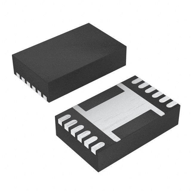
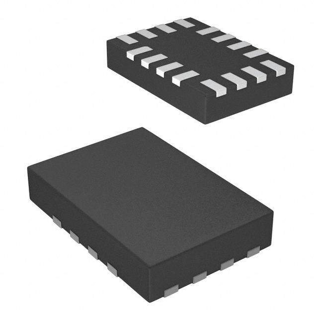
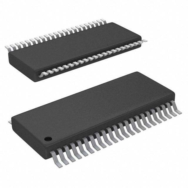
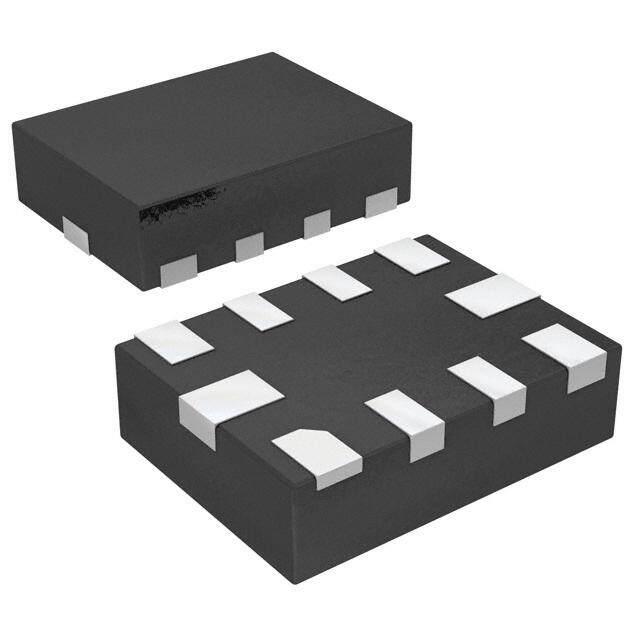
| 供应商器件封装 | 14-TDFN-EP(3x5) |
| 功能 | 燃料,电量检测计/监控器 |
| 包装 | 管件 |
| 商标 | Maxim Integrated |
| 安装类型 | 表面贴装 |
| 安装风格 | SMD/SMT |
| 封装 | Bulk |
| 封装/外壳 | 14-WFDFN 裸露焊盘 |
| 封装/箱体 | DFN-14 |
| 工作温度 | -20°C ~ 70°C |
| 工作电源电压 | 4 V to 9.2 V |
| 工作电源电流 | 80 uA |
| 最大工作温度 | + 70 C |
| 最小工作温度 | - 20 C |
| 标准包装 | 1 |
| 温度监测 | No Temperature Monitoring |
| 电压-电源 | 4 V ~ 9.2 V |
| 电池化学 | 锂离子,锂聚合物 |
| 电池类型 | Li-Ion, Li-Poly |
| 电荷安全定时器 | No Charge Safety Timers |
| 系列 | DS2777G |
| 输出电压 | 4.7 V |
| 零件号别名 | 90-2777G+000 |


PDF Datasheet 数据手册内容提取
19-4688; Rev 4; 6/11 2-Cell, Stand-Alone, Li+ Fuel-Gauge IC with Protector and Optional SHA-1 Authentication General Description Features D The DS2775–DS2778 report available capacity for ♦ High-Side nFET Drivers and Protection Circuitry S rechargeable lithium-ion (Li+) and Li+ polymer (Li-Poly) 2 batteries in mAh and as a percentage of full. Safe oper- ♦ Precision Voltage, Temperature, and Current 7 ation is ensured by the integrated Li+ protector. The Measurement System 7 DS2776/DS2778 support SHA-1-based challenge- ♦ Cell-Capacity Estimation from Coulomb Count, response authentication in addition to all other DS2775/ 5 Discharge Rate, Temperature, and Cell DS2777 features. / Characteristics D Precision measurements of voltage, temperature, and ♦ Estimates Cell Aging Between Learn Cycles S current, along with a cell characteristics table and application parameters, are used for capacity estima- ♦ Uses Low-Cost Sense Resistor 2 tion calculations. The capacity registers report a con- 7 ♦ Allows Calibration of Gain and Temperature servative estimate of the amount of charge that can be 7 removed given the current temperature, discharge rate, Coefficient 6 stored charge, and application parameters. ♦ Programmable Thresholds for Overvoltage and / The DS2775–DS2778 operate from +4.0V to +9.2V for Overcurrent D direct integration into battery packs with two Li+ or Li- ♦ Pack Authentication Using SHA-1 Algorithm S Poly cells. 2 (DS2776/DS2778) In addition to nonvolatile storage for cell compensation 7 and application parameters, the DS2775–DS2778 offer ♦ 32-Byte Parameter EEPROM 7 16 bytes of EEPROM for use by the host system and/or ♦ 16-Byte User EEPROM 7 pack manufacturer to store battery lot and date tracking information. The EEPROM can also be used for non- ♦ Maxim 1-Wire Interface with 64-Bit Unique ID / D volatile storage of system and/or battery usage statis- (DS2775/DS2776) S tics. A Maxim 1-Wire® (DS2775/DS2776) or 2-wire ♦ 2-Wire Interface with 64-Bit Unique ID (DS2777/DS2778) interface provides serial communica- 2 (DS2777/DS2778) tion to access measurement and capacity data regis- 7 ters, control registers, and user memory. The ♦ 3mm x 5mm, 14-Pin TDFN Lead-Free Package 7 DS2776/DS2778 use the SHA-1 hash algorithm in a 8 challenge-response pack authentication protocol for Ordering Information battery-pack verification. PART PIN-PACKAGE TOP MARK Applications DS2775G+ 14 TDFN-EP* D2775 Low-Cost Notebooks DS2775G+T&R 14 TDFN-EP* D2775 UMPCs DS2776G+ 14 TDFN-EP* D2776 DSLR Cameras DS776G+T&R 14 TDFN-EP* D2776 DS2777G+ 14 TDFN-EP* D2777 Video Cameras DS2777G+T&R 14 TDFN-EP* D2777 Commercial and Military Radios DS2778G+ 14 TDFN-EP* D2778 Portable Medical Equipment DS2778G+T&R 14 TDFN-EP* D2778 Note:All devices are specified over the -20°C to +70°C oper- ating temperature range. +Denotes a lead(Pb)-free/RoHS-compliant package. Selector Guide appears at end of data sheet. T&R = Tape and reel. *EP = Exposed pad. 1-Wire is a registered trademark of Maxim Integrated Products, Inc. ________________________________________________________________Maxim Integrated Products 1 For pricing, delivery, and ordering information,please contact Maxim Directat 1-888-629-4642, or visit Maxim’s website at www.maxim-ic.com.
2-Cell, Stand-Alone, Li+ Fuel-Gauge IC with Protector and Optional SHA-1 Authentication 8 ABSOLUTE MAXIMUM RATINGS 7 Voltage Range on PLS, CP, CC, DC Pins Continuous Sink Current, PIO, DQ......................................20mA 7 Relative to VSS.....................................................-0.3V to +18V Continuous Sink Current, CC, DC.......................................10mA 2 Voltage Range on VDD, VIN1, VIN2, SRC Pins Operating Temperature Range...........................-20°C to +70°C S Relative to VSS....................................................-0.3V to +9.2V Storage Temperature Range.............................-55°C to +125°C Voltage Range on All Other Pins Relative to VSS..-0.3V to +6.0V Lead Temperature (soldering, 10s).................................+300°C D Soldering Temperature (reflow).......................................+260°C / 7 Stresses beyond those listed under “Absolute Maximum Ratings” may cause permanent damage to the device. These are stress ratings only, and functional operation of the device at these or any other conditions beyond those indicated in the operational sections of the specifications is not implied. Exposure to 7 absolute maximum rating conditions for extended periods may affect device reliability. 7 2 ELECTRICAL CHARACTERISTICS S D (VDD= +4.0V to +9.2V, TA= -20°C to +70°C, unless otherwise noted. Typical values are at TA= +25°C.) / PARAMETER SYMBOL CONDITIONS MIN TYP MAX UNITS 6 7 IDD0 Sleep mode, TA(cid:1) +50°C 3 5 7 Supply Current Sleep mode, TA> +50°C 10 μA 2 IDD1 Active mode 80 135 S IDD2 Active mode during SHA-1 computation 120 300 D Temperature Accuracy TERR -3 +3 °C / 2.0V (cid:1) VIN1(cid:1) 4.6V, 2.0V (cid:1) (VIN2 - VIN1)(cid:1) -35 +35 5 4.6V, 0°C (cid:1) TA(cid:1) +50°C 7 Voltage Accuracy 2.0V (cid:1) VIN1(cid:1) 4.6V, 2.0V (cid:1) (VIN2 – VIN1)(cid:1) mV 7 -22 22 4.6V, TA = +25°C 2 2.0V (cid:1) VIN1(cid:1) 4.6V, 2.0V (cid:1) (VIN2 - VIN1)(cid:1) 4.6V -50 +50 S Input Resistance (VIN1, VIN2) 15 M(cid:2) D Current Resolution ILSB 1.56 μV Current Full Scale IFS -51.2 +51.2 mV Current Gain Error IGERR -1 +1 % FS Current Offset IOERR 0°C (cid:1) TA(cid:1) +70°C (Note 1) -9.375 9.375 μVh Accumulated Current Offset qOERR 0°C (cid:1) TA(cid:1) +70°C (Note 1) -255 0 μVh/Day 0°C (cid:1) TA(cid:1) +50°C -2 +2 Time-Base Error tERR % -3 +3 CP Output Voltage (VCP - VSRC) VGS IOUT = 0.9μA 4.4 4.7 5 V CP Startup Time tSCP CE = 0, DE = 0, CCP = 0.1μF, active mode 200 ms Output High: CC, DC VOHCP IOH = 100μA (Note 2) VCP - 0.4 V Output Low: CC VOLCC IOL = 100μA VSRC + 0.1 V Output Low: DC VOLDC IOL = 100μA VSRC + 0.1 V DQ, PIO Voltage Range -0.3 +5.5 V DQ, PIO, SDA, SCL Input VIH 1.5 V Logic-High DQ, PIO, SDA, SCL Input VIL 0.6 V Logic-Low OVD Input Logic-High VIH VBAT - 0.2 V OVD Input Logic-Low VIL VSS + 0.2 V 2 _______________________________________________________________________________________
2-Cell, Stand-Alone, Li+ Fuel-Gauge IC with Protector and Optional SHA-1 Authentication ELECTRICAL CHARACTERISTICS (continued) D (VDD= +4.0V to +9.2V, TA= -20°C to +70°C, unless otherwise noted. Typical values are at TA= +25°C.) S 2 PARAMETER SYMBOL CONDITIONS MIN TYP MAX UNITS 7 DQ, PIO, SDA Output Logic-Low VOL IOL = 4mA 0.4 V 7 DQ, PIO Pullup Current IPU Sleep mode, VPIN = (VDD - 0.4V) 30 100 200 nA 5 DQ, PIO, SDA, SCL Pulldown Current IPD Active mode, VPIN = 0.4V 30 100 200 nA /D DQ Input Capacitance CDQ 50 pF S DQ Sleep Timeout tSLEEP DQ < VIL 2 9 s 2 PIO, DQ Wake Debounce tWDB Sleep mode 100 ms 7 7 6 SHA-1 COMPUTATION TIMING (DS2776/DS2778 ONLY) / (VDD= +4.0V to +9.2V, TA= 0°C to +70°C, unless otherwise noted. Typical values are at TA= +25°C.) D S PARAMETER SYMBOL CONDITIONS MIN TYP MAX UNITS 2 Computation Time tCOMP 30 ms 7 7 ELECTRICAL CHARACTERISTICS: PROTECTION CIRCUIT 7 / (VDD= +4.0V to +9.2V, TA= 0°C to +50°C, unless otherwise noted. Typical values are at TA= +25°C.) D PARAMETER SYMBOL CONDITIONS MIN TYP MAX UNITS S VOV = 1110111b 4.438 4.473 4.508 2 Overvoltage Detect VOV VOV = 1100011b 4.242 4.277 4.312 V 7 Charge-Enable Voltage VCE Relative to VOV -100 mV 7 8 Programmable in Control register 0x60h, Undervoltage Detect VUV 2.415 2.450 2.485 V UV[1:0] = 10 OC = 11b -60 -75 -90 Overcurrent Detect: Charge VCOC mV OC = 00b -12.5 -25 -38 OC = 11b 80 100 120 Overcurrent Detect: Discharge VDOC mV OC = 00b 25 38 50 SC =1b 240 300 360 Short-Circuit Current Detect VSC mV SC = 0b 120 150 180 Overvoltage Delay tOVD (Note 3) 600 1400 ms Undervoltage Delay tUVD (Note 3) 600 1400 ms Overcurrent Delay tOCD 8 10 12 ms Short-Circuit Delay tSCD 80 120 160 μs Charger-Detect Hysteresis VCD VUV condition 50 mV Test Threshold VTP COC, DOC condition 0.4 1.0 1.2 V DOC condition 20 40 80 Test Current ITST μA COC condition -45 -60 -95 PLS Pulldown Current IPPD Sleep mode 200 400 630 μA VUV condition, max: VPLS = 15V, VDD = 1.4V; Recovery Current IRC 3.3 8 13 mA min: VPLS = 4.2V, VDD = 2V _______________________________________________________________________________________ 3
2-Cell, Stand-Alone, Li+ Fuel-Gauge IC with Protector and Optional SHA-1 Authentication 8 EEPROM RELIABILITY SPECIFICATION 7 (VDD= +4.0V to +9.2V, TA= -20°C to +70°C, unless otherwise noted.) 7 2 PARAMETER SYMBOL CONDITIONS MIN TYP MAX UNITS S EEPROM Copy Time tEEC 10 ms D EEPROM Copy Endurance NEEC TA = +50°C 50,000 Cycles / 7 7 ELECTRICAL CHARACTERISTICS: 1-Wire INTERFACE, STANDARD (DS2775/DS2776 ONLY) 7 (VDD= +4.0V to +9.2V, TA= -20°C to +70°C.) 2 S PARAMETER SYMBOL CONDITIONS MIN TYP MAX UNITS D Time Slot tSLOT 60 120 μs / Recovery Time tREC 1 μs 6 7 Write-Zero Low Time tLOW0 60 120 μs 7 Write-One Low Time tLOW1 1 15 μs 2 Read Data Valid tRDV 15 μs S Reset Time High tRSTH 480 μs D Reset Time Low tRSTL 480 960 μs / Presence-Detect High tPDH 15 60 μs 5 Presence-Detect Low tPDL 60 240 μs 7 7 2 ELECTRICAL CHARACTERISTICS: 1-Wire INTERFACE, OVERDRIVE (DS2775/DS2776 ONLY) S D (VDD= +4.0V to +9.2V, TA= -20°C to +70°C.) PARAMETER SYMBOL CONDITIONS MIN TYP MAX UNITS Time Slot tSLOT 6 16 μs Recovery Time tREC 1 μs Write-Zero Low Time tLOW0 6 16 μs Write-One Low Time tLOW1 1 2 μs Read Data Valid tRDV 2 μs Reset Time High tRSTH 48 μs Reset Time Low tRSTL 48 80 μs Presence-Detect High tPDH 2 6 μs Presence-Detect Low tPDL 8 24 μs 4 _______________________________________________________________________________________
2-Cell, Stand-Alone, Li+ Fuel-Gauge IC with Protector and Optional SHA-1 Authentication ELECTRICAL CHARACTERISTICS: 2-WIRE INTERFACE (DS2777/DS2778 ONLY) D (VDD= +4.0V to +9.2V, TA= -20°C to +70°C.) S 2 PARAMETER SYMBOL CONDITIONS MIN TYP MAX UNITS 7 SCL Clock Frequency fSCL (Note 4) 0 400 kHz 7 Bus-Free Time Between a STOP tBUF 1.3 μs 5 and START Condition / Hold Time (Repeated) START D tHD:STA (Note 5) 0.6 μs Condition S Low Period of SCL Clock tLOW 1.3 μs 2 High Period of SCL Clock tHIGH 0.6 μs 7 Setup Time for a Repeated 7 tSU:STA 0.6 μs START Condition 6 Data Hold Time tHD:DAT (Notes 6, 7) 0 0.9 μs /D Data Setup Time tSU:DAT (Note 6) 100 ns S Rise Time of Both SDA and SCL 20 + tR 300 ns 2 Signals 0.1CB 7 Fall Time of Both SDA and SCL 20 + tF 300 ns 7 Signals 0.1CB 7 Setup Time for STOP Condition tSU:STO 0.6 μs / D Spike Pulse Widths Suppressed by Input Filter tSP (Note 8) 0 50 ns S 2 Capacitive Load for Each Bus Line CB (Note 9) 400 pF 7 7 SCL, SDA Input Capacitance CBIN 60 pF 8 Note 1: Accumulation bias and offset bias registers set to 00h. NBEN bit set to 0. Note 2: Measurement made with VSRC= +8V, VGSdriven with external +4.5V supply. Note 3: Overvoltage (OV) and undervoltage (UV) delays (tOVD, tUVD) are reduced to zero seconds if the OV or UV condition is detected within 100ms of entering active mode. Note 4: Timing must be fast enough to prevent the DS2777/DS2778 from entering sleep mode due to bus low for period > tSLEEP. Note 5: fSCLmust meet the minimum clock low time plus the rise/fall times. Note 6: The maximum tHD:DATneed only be met if the device does not stretch the low period (tLOW) of the SCL signal. Note 7: This device internally provides a hold time of at least 75ns for the SDA signal (referred to the VIHMINof the SCL signal) to bridge the undefined region of the falling edge of SCL. Note 8: Filters on SDA and SCL suppress noise spikes at the input buffers and delay the sampling instant. Note 9: CBis total capacitance of one bus line in pF. _______________________________________________________________________________________ 5
2-Cell, Stand-Alone, Li+ Fuel-Gauge IC with Protector and Optional SHA-1 Authentication 8 Typical Operating Characteristics 7 (TA = +25°C, unless otherwise noted.) 7 2 DISCHARGE-OVERCURRENT CC FET GATE TURN-OFF DURING S PROTECTION DELAY CHARGE-OVERCURRENT EVENT DS2775/6/7/8 toc01 DS2775/6/7/8 toc02 D 2V/div 2V/div CC FET GATE / DC FET 7 0V GATE 0V 7 2V/div 2V/div CSOCU FRECTE 7 DC FET 0V 0V SOURCE 2 1V/div 1V/div S D 0V VGS 0V VGS CC FET / 20mV/d0iVv VSSENNSS E2 5RmEΩSISTOR 0V VSSENNSS E2 5RmEΩSISTOR 6 WITH DISCHARGE- 20mV/div WITH CHARGE- 7 OVERCURRENT OVERCURRENT 0 2 4 6 8 10 12 14 16 18 20 THRESHOLD = 38mV 0 5 10 15 20 25 30 35 40 45 50 THRESHOLD = 25mV 7 TIME (ms) TIME (μs) 2 SHORT-CIRCUIT PROTECTION S DC FET GATE TURN-OFF DURING DELAY SHORT-CIRCUIT EVENT D DS2775/6/7/8 toc04 DS2775/6/7/8 toc03 5/ 2V/div 2V/div DC FET 7 0V DGCAT FEET 0V GATE 7 2V/div 2V/div DC FET 2 DC FET 0V 0V SOURCE SOURCE S 1V/div 1V/div D 0V VGS DC FET 0V VGS DC FET 50mV/div VSSENNSS E2 5RmEΩSISTOR 100mV/div SVSENNSS E2 5RmEΩSISTOR 0V WITH SHORT-CIRCUIT 0V WITH SHORT-CIRCUIT THRESHOLD = 150mV THRESHOLD = 150mV 0 20 40 60 80 100 120 140 160 180 200 0 2 4 6 8 10 12 14 16 18 20 TIME (μs) TIME (μs) VOLTAGE MEASUREMENT CHARGE-PUMP STARTUP EXITING SLEEP ACCURACY MODE (VDD = 8V NO LOAD ON PK+) 11124680 -20°C DS2775/6/7/8 toc05 678 12.6V DS2775/6/7/8 toc06 CCURACY (mV) 11802 +70°C +25°C VOLTAGE (V) 345 A 2.75V 6 2 4 2 0 0 -2 0 1 2 3 4 0 10 20 30 40 50 60 70 80 90 100 VINX (V) TIME (ms) 6 _______________________________________________________________________________________
2-Cell, Stand-Alone, Li+ Fuel-Gauge IC with Protector and Optional SHA-1 Authentication Typical Operating Characteristics (continued) D (TA = +25°C, unless otherwise noted.) S 2 CURRENT MEASUREMENT CURRENT MEASUREMENT OFFSET ACCURACY IRC vs. VDD vs. TEMPERATURE 7 17255 -20°C DS2775/6/7/8 toc07 567 1kΩ RESISTOR FROM PLS TO PK+ DS2775/6/7/8 toc08 012 DS2775/6/7/8 toc09 75/D μCCURACY (V) -2255 +25°C I (mA)RC 34 μSB (1.5625V) --21 S27 A +70°C L 7 2 -3 -75 6 1 -4 / D -125 0 -5 -0.052 -0.032 -0.012 0.008 0.028 0.048 0 1 2 3 4 5 6 -20 0 20 40 60 S VSNS (mV) VDD (V) TEMPERATURE (°C) 2 7 7 7 / D S 2 7 7 8 _______________________________________________________________________________________ 7
2-Cell, Stand-Alone, Li+ Fuel-Gauge IC with Protector and Optional SHA-1 Authentication 8 Pin Configuration 7 7 TOP VIEW 2 S CC 1 + 14 CP D VDD 2 13 SRC / DC 3 DS2775 12 SCL/OVD 7 VIN2 4 DS2776 11 SDA/DQ 7 VIN1 5 DS2777 10 PLS DS2778 7 VB 6 9 PIO EP 2 VSS 7 8 SNS S TDFN D (3mm × 5mm) / 6 7 7 Pin Description 2 S PIN NAME FUNCTION D 1 CC Charge Control. Charge FET control output. / 5 2 VDD Chip-Supply Input. Bypass with 0.1μF to VSS. 7 3 DC Discharge Control. Discharge FET control output. 7 2 Battery Voltage Sense Input 2. Connect to highest voltage potential positive cell terminal through 4 VIN2 decoupling network. S D Battery Voltage Sense Input 1. Connect to lowest voltage potential positive cell terminal through 5 VIN1 decoupling network. 6 VB Regulated Operating Voltage. Bypass with 0.1μF to VSS. 7 VSS Device Ground. Chip ground and battery-side sense resistor input. 8 SNS Sense Resistor Connection. Pack-side sense resistor sense input. 9 PIO Programmable I/O. Can be configured as wake input. Pack Plus Terminal Sense Input. Used to detect the removal of short-circuit, discharge overcurrent, and 10 PLS charge overcurrent conditions. Data Input/Output. Serial data I/O, includes weak pulldown to detect system disconnect and can be 11 SDA/DQ configured as wake input for 1-Wire devices. Serial Clock Input/Overdrive Select. Communication clock for 2-wire devices/overdrive select pin for 12 SCL/OVD 1-Wire devices. 13 SRC Protection MOSFET Source Connection. Used as a reference for the charge pump. 14 CP Charge Pump Output. Generates gate drive voltage for protection FETs. Bypass with 0.47μF to SRC. — EP Exposed Pad. Connect to ground or leave unconnected. 8 _______________________________________________________________________________________
2-Cell, Stand-Alone, Li+ Fuel-Gauge IC with Protector and Optional SHA-1 Authentication Block Diagram D S 2 7 7 VOLTAGE 10-BIT + SIGN VIN2 5 POCWOENRT-RMOOLDE TEMPERATURE ADC/MUX VIN1 /D Li+ S PLS PROTECTOR 2 15-BIT + SIGN SNS CURRENT 7 ADC 7 6 FuelPack™ PRECISION ANALOG ALGORITHM OSCILLATOR VREF VSS /D CC S FET DRIVERS DC 2 7 CONTROL AND CP STATUS REGISTERS 7 PIN PIO LOGIC DRIVERS SDA/DQ 7 CHARGE VDD PUMP 32-BYTE AND SCL/OVD / PARAMETER POWER D EEPROM SWITCH PIO COMMUNICATION CONTROL S INTERFACE VOLTAGE 16-BYTE USER 2 REGULATOR EEPROM 7 VB 7 DS2775–DS2778 8 VB INTERNAL FuelPack is a trademark of Maxim Integrated Products, Inc. _______________________________________________________________________________________ 9
2-Cell, Stand-Alone, Li+ Fuel-Gauge IC with Protector and Optional SHA-1 Authentication 8 DS2775/DS2776 Typical Application Circuit 7 7 2 S PK+ D / 7 1kΩ 1kΩ 470Ω 1kΩ 150Ω 1kΩ 7 7 CC SRC DC 2 150Ω PLS VDD S DATA DQ VIN2 1kΩ DS2775 VIN1 D PIO DS2776 CP 6/ 5.1V 0.1μF VB SNS VSS OVD 0.47μF 0.1μF 7 SRC 7 RSNS PK- 2 S D / 5 7 DS2777/DS2778 Typical Application Circuit 7 2 S D PK+ 1kΩ 1kΩ 470Ω 1kΩ 150Ω 1kΩ CC SRC DC 150Ω PLS VDD SDA SDA VIN2 1kΩ SCL SCL DS2777 VIN1 150Ω PIO DS2778 CP VB 0.47μF 5.1V 5.1V 0.1μF SNS VSS 0.1μF SRC RSNS PK- 10 ______________________________________________________________________________________
2-Cell, Stand-Alone, Li+ Fuel-Gauge IC with Protector and Optional SHA-1 Authentication Detailed Description serve power by disabling measurement and capacity D estimation functions, but preserve register contents. The DS2775–DS2778 function as an accurate fuel S Gate drive to the protection FETs is disabled in sleep; gauge, Li+ protector, and SHA-1-based authentication the SHA-1 authentication feature is not operational. 2 token (SHA-1-based authentication available only on 7 the DS2776/DS2778). The fuel gauge provides accu- The IC enters sleep mode under two different condi- rate estimates of remaining capacity and reports timely tions: bus low and undervoltage. An enable bit makes 7 voltage, temperature, and current measurement data. entry into sleep optional for each condition. Sleep mode 5 Capacity estimates are calculated from a piecewise lin- is not entered if a charger is connected (VPLS > VDD + / D ear model of the battery performance over load and VCD) or if a charge current of 1.6mV/RSNS measured temperature along with system parameters for charge from SNS to VSS. The DS2775–DS2778 exit sleep mode S and end-of-discharge conditions. The algorithm para- upon charger connection or a low-to-high transition on 2 meters are user programmable and can be modified any communication line. The bus-low condition, where 7 within the pack. Critical capacity and aging data are all communication lines are low for tSLEEP, indicates periodically saved to EEPROM in case of short-circuit pack removal or system shutdown in which the bus 7 or deep-depletion events. pullup voltage, VPULLUP, is not present. The power 6 mode (PMOD) bit must be set to enter sleep when a / The Li+ protection function ensures safe, high-perfor- D bus-low condition occurs. After the DS2775–DS2778 mance operation. nFET protection switches are driven enter sleep due to a bus-low condition, it is assumed S with a charge pump that maintains gate drive as the cell voltage decreases. The high-side topology pre- that no charge or discharge current flows and that 2 coulomb counting is unnecessary. serves the ground path for serial communication while 7 eliminating the parasitic charge path formed when the The second condition to enter sleep is an undervoltage 7 fuel-gauge IC is located inside the protection FETs in a condition, which reduces battery drain due to the 7 low-side configuration. The thresholds for overvoltage, DS2775–DS2778 supply current and prevents overdis- / undervoltage, overcurrent, and short-circuit current are charging the cell. The DS2775–DS2778 transition to D user programmable for customization to each cell and sleep mode if the VIN1 or VIN2 voltage is less than VUV S application. and the undervoltage enable (UVEN) bit is set. The communication bus must be in a static state, that is, 2 The 32-bit-wide SHA-1 engine with 64-bit secret and with DQ (SDA and SCL for 2-wire) either high or low for 7 64-bit challenge words resists brute force and other tSLEEP. The DS2775–DS2778 transition from sleep 7 attacks with financial-level HMAC security. The chal- mode to active mode when DQ (SDA and SCL for lenge of managing secrets in the supply chain is 8 2-wire) changes logic state. See Figures 1 and 2 for addressed with the compute next secret feature. The more information on sleep-mode state. unique serial number or ROM ID can be used to assign a unique secret to each battery. The DS2775–DS2778 have a “power switch” capability for waking the device and enabling the protection FETs Power Modes when the host system is powered down. A simple dry The DS2775–DS2778 have two power modes: active contact switch on the PIO pin or DQ pin can be used to and sleep. On initial power-up, the DS2775–DS2778 wake up the battery pack. The power-switch function is default to active mode. In active mode, the DS2775– enabled using the PSPIO and PSDQ configuration bits DS2778 are fully functional with measurements and in the Control register. capacity estimation registers continuously updated. When PSPIO or PSDQ are set and sleep mode is The protector circuit monitors battery pack, cell volt- entered through the PMOD condition*, the PIO and DQ ages, and battery current for safe conditions. The pro- pins pull high, respectively. Sleep mode is exited upon tection FET gate drivers are enabled when conditions the detection of a low-going transition on PIO or DQ. are deemed safe. Also, the SHA-1 authentication func- PIO has a 100ms debounce period to filter out glitches tion is available in active mode. When an SHA-1 com- that can be caused when a sleeping battery is inserted putation is performed, the supply current increases to into a system. IDD2for tSHA. In sleep mode, the DS2775–DS2778 con- *The “power switch” feature is disabled if sleep mode is entered because of a UV condition. ______________________________________________________________________________________ 11
2-Cell, Stand-Alone, Li+ Fuel-Gauge IC with Protector and Optional SHA-1 Authentication 8 7 7 ACTIVE SLEEP RISING EDGE ON SDA OR SCL 2 ACTIVE RISING EDGE ON DQ SLEEP PMOD = 0 PSPIO = 0 PMOD = 0 PSPIO = 0 UVEN = 0 PSDQ = X S UVEN = 0 PSDQ = 0 CHARGER DETECT D CHARGER DETECT 7/ VIN1 OR VIN2 < VUV PULL DQ LOW 7 ACTIVE SLEEP RISING EDGE ON SDA OR SCL 7 ACTIVE VIN1 OR VIN2 < VUV SLEEP PMOD = 0 PSPIO = 0 PMOD = 0 PSPIO = 0 UVEN = 1 PSDQ = X 2 UVEN = 1 PSDQ = 1 CHARGER DETECT S CHARGER DETECT D PULL PIO LOW / PULL PIO LOW 6 ACTIVE SLEEP RISING EDGE ON SDA OR SCL 7 ACTIVE PULL DQ LOW FOR tSLEEP SLEEP PMOD = 1 PSPIO = 1 7 PMOD = 1 PSPIO = 1 UVEN = 0 PSDQ = X UVEN = 0 PSDQ = 0 CHARGER DETECT 2 RISING EDGE ON DQ PULL SDA AND SCL LOW S CHARGER DETECT FOR tSLEEP D / 5 PULL PIO LOW VIN1 OR VIN2 < VUV 7 PULL DQ LOW FOR tSLEEP PULL PIO LOW 7 2 ACTIVE VIN1 OR VIN2 < VUV SLEEP ACTIVE RISING EDGE ON SDA OR SCL SLEEP PMOD = 1 PSPIO = 1 PMOD = 1 PSPIO = 1 S UVEN = 1 PSDQ = 1 UVEN = 1 PSDQ = X D PULL DQ LOW CHARGER DETECT CHARGER DETECT PULL SDA AND SCL LOW FOR tSLEEP Figure 1. Sleep-Mode State Diagram for DS2775/DS2776 Figure 2. Sleep-Mode State Diagram for DS2777/DS2778 Li+ Protection Circuitry Overvoltage (OV) If either of the voltages on (VIN2 - VIN1) or (VIN1 - VSS) During active mode, the DS2775–DS2778 constantly exceeds the overvoltage threshold, VOV, for a period monitor SNS, VIN1, VIN2, and PLS to protect the battery longer than overvoltage delay, tOVD, the CC pin is dri- from overvoltage (overcharge), undervoltage (overdis- ven low to shut off the external charge FET. The DC out- charge), and excessive charge and discharge currents put remains high during overvoltage to allow (overcurrent, short circuit). Table 1 summarizes the discharging. When (VIN2 - VIN1) and (VIN1 - VSS) falls conditions that activate the protection circuit, the below the charge-enable threshold, VCE, the response of the DS2775–DS2778, and the thresholds DS2775–DS2778 turn the charge FET on by driving CC that release the DS2775–DS2778 from a protection high. The DS2775–DS2778 drive CC high before state. Figure 3 shows Li+ protection circuitry example [(VIN2 - VIN1) and (VIN1 - VSS)] < VCE if a discharge waveforms. condition persists with VSNS ≥ 1.2mV and [(VIN2 - VIN1) and (VIN1- VSS)] < VOV. 12 ______________________________________________________________________________________
2-Cell, Stand-Alone, Li+ Fuel-Gauge IC with Protector and Optional SHA-1 Authentication Table 1. Li+ Protection Conditions and DS2775/DS2776 Responses D ACTIVATION S CONDITION RELEASE THRESHOLD THRESHOLD DELAY RESPONSE 2 7 Both VCELL < VCE or 7 Overvoltage (OV) (Note 1) VCELL > VOV tOVD CC Off (VSNS(cid:1) 1.2mV and both VCELL < VOV) (Note 1) 5 / VPLS > VIN2 (charger connected) D CC Off, DC Off, Undervoltage (UV) (Note 1) VCELL < VUV tUVD or (both VCELL > VUV and S Sleep Mode (Note 2) UVEN = 0) (Note 3) 2 VPLS < VDD – VTP 7 Overcurrent, Charge (COC) VSNS < VCOC tOCD CC Off, DC Off (charger removed) (Note 4) 7 Overcurrent, Discharge VPLS > VDD – VTP 6 VSNS > VDOC tOCD DC Off (DOC) (load removed) (Note 5) / D Short Circuit (SC) VSNS > VSC tSCD DC Off VPLS > VDD – VTP (Note 5) S Note 1:VCELLis defined as (VIN1- VSS) or (VIN2- VIN1). 2 Note 2:Sleep mode is only entered if UVEN = 1. Note 3:If VCELL< VUVwhen a charger connection is detected, release is delayed until VCELL≥VUV. The recovery charge path pro- 7 vides an internal current limit (IRC) to safely charge the battery. 7 Note 4:With test current IPPDflowing from PLS to VSS(pulldown on PLS) enabled. 7 Note 5:With test current ITSTflowing from VDDto PLS (pullup on PLS). / D S 2 VOV VCE 7 VIN 7 VUV 8 DISCHARGE VSC VDOC VSNS 0 -VCOC CHARGE VOHCC VCP CC tOVD tOVD tOCD tUVD VDD VCP DC tSCO tOCD tUVD VPLS ACTIVE POWER MODE SLEEP* *IF UVEN = 1. Figure 3. Li+ Protection Circuitry Example Waveforms ______________________________________________________________________________________ 13
2-Cell, Stand-Alone, Li+ Fuel-Gauge IC with Protector and Optional SHA-1 Authentication 8 Undervoltage (UV) The DS2775–DS2778 provide a test current of value 7 If the average of the voltages on (VIN2 - VIN1) or ITSTfrom VDD to PLS, pulling PLS up, in order to detect 7 (VIN1 - VSS) drops below the undervoltage threshold, the removal of the offending low-impedance load. 2 VUV, for a period longer than undervoltage delay, tUVD, Short Circuit (SC) the DS2775–DS2778 shut off the charge and discharge S FETs. If UVEN is set, the DS2775–DS2778 also enter If VSNS exceeds short-circuit threshold, VSC, for a D sleep mode. When a charger is detected and VPLS > period longer than short-circuit delay, tSCD, the DS2775–DS2778 shut off the external discharge FET. / VIN2, the DS2775–DS2778 provide a current-limited 7 recovery charge path (IRC) from PLS to VDD to gently The discharge current path is not reestablished until 7 charge severely depleted cells. The recovery charge the voltage on PLS rises above (VDD - VTP). The 7 path is enabled when 0 ≤ [(VIN2 - VIN1) and (VIN1 - DS2775–DS2778 provide a test current of value ITST 2 VSS)] < VCE. The FETs remain off until (VIN2- VIN1) and from VDDto PLS, pulling PLS up, in order to detect the removal of the short circuit. (VIN1- VSS) exceed VUV. S All the protection conditions described are logic D Overcurrent, Charge Direction (COC) ANDed to affect the CC and DC outputs. Charge current develops a negative voltage on VSNS / CC = (overvoltage) AND(undervoltage) AND 6 with respect to VSS. If VSNS is less than the charge (overcurrent, charge direction) AND(Protection register 7 overcurrent threshold, VCOC, for a period longer than bit CE = 0) 7 overcurrent delay, tOCD, the DS2775–DS2778 shut off both external FETs. The charge current path is not re- DC = (undervoltage) AND(overcurrent, either direction) 2 established until the voltage on the PLS pin drops AND(short circuit) AND(Protection register bit S below (VDD - VTP). The DS2775–DS2778 provide a test DE = 0) D current of value IPPD from PLS to VSS, pulling PLS Voltage Measurements down, in order to detect the removal of the offending / 5 charge current source. Cell voltages are measured every 440ms. The lowest 7 potential cell, VIN1, is measured with respect to VSS. Overcurrent, Discharge Direction (DOC) 7 The highest potential cell, VIN2, is measured with 2 Dwiisthc hraersgpee ccut rtroe nVt SdSe.v Iefl oVpSsN aS peoxscietiveed sv otlhtaeg de isocnh VaSrgNeS rreasnpgeec ot f to-5 VV INto1 .+ B4.a9t9te5r1yV v aonltadg ae sre asroelu mtioena souf r4e.d8 8w2i8thm Va S overcurrent threshold, VDOC, for a period longer than and placed in the Result register in two’s complement D tOCD, the DS2775–DS2778 shut off the external dis- form. Voltages above the maximum register value are charge FET. The discharge current path is not reestab- reported as 7FE0h. lished until the voltage on PLS rises above (VDD - VTP). MSB - ADDRESS 0Ch, VIN1 - VSS LSB - ADDRESS 0Dh, VIN1 - VSS MSB - ADDRESS 1Ch, VIN2 - VIN1 LSB - ADDRESS 1Dh, VIN2 - VIN1 S 29 28 27 26 25 24 23 22 21 20 X X X X X MSb LSb MSb LSb “S”: SIGN BIT(S), “X”: RESERVED UNITS: 4.883mV Figure 4. Voltage Register Format 14 ______________________________________________________________________________________
2-Cell, Stand-Alone, Li+ Fuel-Gauge IC with Protector and Optional SHA-1 Authentication Temperature Measurement 1.5625µV. The input linearly converts peak signal ampli- D tudes up to 102.4mV as long as the continuous signal The DS2775–DS2778 use an integrated temperature S level (average over the conversion cycle period) does sensor to measure battery temperature with a resolution not exceed ±51.2mV. The ADC samples the input differ- 2 of 0.125°C. Temperature measurements are updated entially at 18.6kHz and updates the Current register at 7 every 440ms and placed in the Temperature register in the completion of each conversion cycle (3.52s). Charge 7 two’s complement form. currents above the maximum register value are reported 5 Current Measurement as 7FFFh. Discharge currents below the minimum regis- / ter value are reported as 8000h. D In active mode, the DS2775–DS2778 continuously mea- sure the current flow into and out of the battery by mea- The Average Current register reports an average cur- S suring the voltage drop across a low-value current-sense rent level over the preceding 28.16s. The register value 2 resistor, RSNS. The voltage-sense range between SNS is updated every 28.16s in two’s complement form and 7 and VSS is ±51.2mV with a least significant bit (LSb) of represents an average of the eight preceding Current register values. 7 6 / D MSB—ADDRESS 0Ah LSB—ADDRESS 0Bh S S 29 28 27 26 25 24 23 22 21 20 X X X X X 2 MSb LSb MSb LSb 7 “S”: SIGN BIT(S), “X”: RESERVED UNITS: 0.125°C 7 Figure 5. Temperature Register Format 7 / D S MSB—ADDRESS 0Eh LSB—ADDRESS 0Fh S 214 213 212 211 210 29 28 27 26 25 24 23 22 21 20 2 7 MSb LSb MSb LSb 7 “S”: SIGN BIT(S) UNITS: 1.5625μV/RSNS 8 Figure 6. Current Register Format MSB—ADDRESS 08h LSB—ADDRESS 09h S 214 213 212 211 210 29 28 27 26 25 24 23 22 21 20 MSb LSb MSb LSb “S”: SIGN BIT(S) UNITS: 1.5625μV/RSNS Figure 7. Average Current Register Format ______________________________________________________________________________________ 15
2-Cell, Stand-Alone, Li+ Fuel-Gauge IC with Protector and Optional SHA-1 Authentication 8 Current Offset Correction Current Blanking 7 Every 1024th conversion, the ADC measures its input The current blanking feature modifies current measure- 7 offset to facilitate offset correction. Offset correction ment result prior to being accumulated in the ACR. 2 occurs approximately once per hour. The resulting cor- Current blanking occurs conditionally when a current S rection factor is applied to the subsequent 1023 mea- measurement (raw current and COBR) falls in one of surements. During the offset correction conversion, the two defined ranges. The first range prevents charge D ADC does not measure the sense resistor signal. A currents less than 100µV from being accumulated. The / maximum error of 1/1024 in the Accumulated Current second range prevents discharge currents less than 7 register (ACR) is possible; however, to reduce the error, 25µV in magnitude from being accumulated. Charge 7 the current measurement made just prior to the offset current blanking is always performed; however, dis- 7 conversion is retained in the Current register and is charge current blanking must be enabled by setting the 2 substituted for the dropped current measurement in the NBEN bit in the Control register. See the Control S current accumulation process. Therefore the accumu- Register Formatdescription for additional information. lated current error due to offset correction is typically D Current Measurement Gain much less than 1/1024. / 6 Current Offset Bias The DS2775–DS2778’s current measurement gain can be adjusted through the RSGAIN register, which is facto- 7 The current offset bias value (COB) allows a program- ry calibrated to meet the data sheet specified accuracy. 7 mable offset value to be added to raw current measure- RSGAIN is user accessible and can be reprogrammed 2 ments. The result of the raw current measurement plus after module or pack manufacture to improve the current S COB is displayed as the current measurement result in measurement accuracy. Adjusting RSGAIN can correct D the Current register and is used for current accumula- for variation in an external sense resistor’s nominal value tion. COB can be used to correct for a static offset error and allows the use of low-cost, nonprecision current- / 5 or can be used to intentionally skew the current results sense resistors. RSGAIN is an 11-bit value stored in 2 7 and therefore the current accumulation. Read and write bytes of the parameter EEPROM memory block. The access is allowed to COB. Whenever the COB is writ- RSGAIN value adjusts the gain from 0 to 1.999 in steps 7 ten, the new value is applied to all subsequent current of 0.001 (precisely 2–10). The user must use caution 2 measurements. COB can be programmed in 1.56µV when programming RSGAIN to ensure accurate current S steps to any value between -199.7µV and +198.1µV. measurement. When shipped from the factory, the gain D The COBR value is stored as a two’s complement value calibration value is stored in two separate locations in the in volatile memory and must be initialized through the parameter EEPROM block, RSGAIN, which is reprogram- interface on power-up. The factory default value is 00h. mable and FRSGAIN, which is read-only. RSGAIN deter- mines the gain used in the current measurement. The ADDRESS 7Bh S 26 25 24 23 22 21 20 MSb LSb “S”: SIGN BIT(S) UNITS: 1.56μV/RSNS Figure 8. Current Offset Bias Register Format MSB—ADDRESS 78h LSB—ADDRESS 79h X SC0 OC1 OC0 X 20 2-1 2-2 2-3 2-4 2-5 2-6 2-7 2-8 2-9 2-10 MSb LSb MSb LSb “X”: RESERVED UNITS: 2–10 Figure 9. RSGAIN Register 16 ______________________________________________________________________________________
2-Cell, Stand-Alone, Li+ Fuel-Gauge IC with Protector and Optional SHA-1 Authentication FRSGAIN value is provided to preserve the factory cali- with the results displayed in the Accumulated Current D bration value only and is not used to calibrate the current register (ACR). The accuracy of the ACR is dependent S measurement. The 16-bit FRSGAIN value is readable on both the current measurement and the conversion from addresses B0h and B1h. time base. The ACR has a range of 0 to +409.6mVh 2 with an LSb of 6.25µVh. Additional registers hold frac- 7 Sense-Resistor Temperature tional results of each accumulation to avoid truncation 7 Compensation errors. The fractional result bits are not user accessible. 5 Accumulation of charge current above the maximum The DS2775–DS2778 can temperature compensate the / register value is reported at the maximum value; con- D current-sense resistor to correct for variation in a sense versely, accumulation of discharge current below the resistor’s value over temperature. The DS2775–DS2778 S minimum register value is reported at the minimum are factory programmed with the sense-resistor temper- 2 value. ature coefficient, RSTC, set to zero, which turns off the 7 temperature compensation function. RSTC is user Charge currents (positive Current register values) less accessible and can be reprogrammed after module or than 100µV are not accumulated in order to mask the 7 pack manufacture to improve the current accuracy effect of accumulating small positive offset errors over 6 when using a high-temperature coefficient current- long periods. This effect limits the minimum charge cur- / D sense resistor. RSTC is an 8-bit value stored in the rent, for coulomb counting purposes, to 5mA for RSNS parameter EEPROM memory block. The RSTC value = 0.020Ωand 20mA for RSNS= 0.005Ω(see Table 2 for S sets the temperature coefficient from 0 to +7782ppm/°C more details). 2 in steps of 30.5ppm/°C. The user must program RSTC Read and write access is allowed to the ACR. The 7 cautiously to ensure accurate current measurement. ACR must be written most significant byte (MSB) first, 7 Temperature compensation adjustments are made when then LSB. Whenever the ACR is written, the fractional 7 the Temperature register crosses 0.5°C boundaries. The accumulation result bits are cleared. The write must / temperature compensation is most effective with the be completed in 3.5s. A write to the ACR forces the D resistor placed as close as possible to the VSS terminal ADC to perform an offset correction conversion and S to optimize thermal coupling of the resistor to the on-chip update the internal offset correction factor. The cur- temperature sensor. If the current shunt is constructed rent measurement and accumulation begin with the 2 with a copper PCB trace, run the trace under the second conversion following a write to the ACR. To 7 DS2775–DS2778 package whenever possible. preserve the ACR value in case of power loss, the 7 ACR value is backed up to EEPROM. The ACR value Current Accumulation 8 is recovered from EEPROM on power-up. See the Current measurements are internally summed, or accu- Memory Mapfor specific address location and back- mulated, at the completion of each conversion period up frequency. MSB—ADDRESS 10h LSB—ADDRESS 11h 215 214 213 212 211 210 29 28 27 26 25 24 23 22 21 20 MSb LSb MSb LSb UNITS: 6.25μV/RSNS Figure 10. Accumulated Current Register Format Table 2. Resolution and Range vs. Sense Resistor RSNS TYPE OF RESOLUTION/RANGE VSS - VSNS 20m(cid:1) 15m(cid:1) 10m(cid:1) 5m(cid:1) Current Resolution 1.5625μV 78.13μA 104.2μA 156.3μA 312.5μA Current Range ±51.2mV ±2.56A ±3.41A ±5.12A ±10.2A ACR Resolution 6.25μVh 312.5μAh 416.7μAh 625μAh 1.250mAh ACR Range ±409.6mVh ±20.48Ah ±27.30Ah ±40.96Ah ±81.92Ah ______________________________________________________________________________________ 17
2-Cell, Stand-Alone, Li+ Fuel-Gauge IC with Protector and Optional SHA-1 Authentication 8 Accumulation Bias Modeling Cell Characteristics 7 In some designs a systematic error or an application To achieve reasonable accuracy in estimating remain- 7 preference requires the application of an arbitrary bias ing capacity, the cell performance characteristics over 2 to the current accumulation process. The Current temperature, load current, and charge-termination point S Accumulation Bias register (CAB) allows a user-pro- must be considered. Since the behavior of Li+ cells is grammed constant positive or negative polarity bias to nonlinear, these characteristics must be included in the D be included in the current accumulation process. The capacity estimation to achieve an acceptable level of / value in CAB can be used to estimate battery currents accuracy in the capacity estimation. The FuelPack 7 that do not flow through the sense resistor, estimate method used in the DS2775–DS2778 is described in 7 battery self-discharge, or estimate current levels below general in Application Note 131: Lithium-Ion Cell Fuel 7 the current measurement resolution. The user-pro- Gauging with Maxim Battery Monitor ICs. To facilitate 2 grammed two’s complement value, with bit weighting efficient implementation in hardware, a modified version S the same as the current register, is added to the ACR of the method outlined in Application Note 131 is used once per current conversion cycle. CAB is loaded on to store cell characteristics in the DS2775–DS2778. Full D power-up from EEPROM memory. and empty points are retrieved in a lookup process that / 6 Cycle Counter retraces a piecewise linear model consisting of three model curves named full, active empty, and standby 7 The cycle counter is an absolute count of the cumula- empty. Each model curve is constructed with five line 7 tive discharge cycles. This register is intended to act as segments, numbered 1 through 5. Above +40°C, the 2 a “cell odometer.” The LSb is two cycles, which allows segment 5 model curves extend infinitely with zero S a maximum count of 510 discharge cycles. The register slope, approximating the nearly flat change in capacity D does not loop. Once the maximum value is reached, of Li+ cells at temperatures above +40°C. Segment 4 of the register is clamped. This register is read and write each model curves originates at +40°C on its upper end / 5 accessible while the parameter EEPROM memory block and extends downward in temperature to the junction 7 (block 1) is unlocked. The Cycle Count register with segment 3. Segment 3 joins with segment 2, which becomes read-only once the EEPROM block is locked. in turn joins with segment 1. Segment 1 of each model 7 curve extends from the junction with segment 2 to infi- 2 Capacity Estimation Algorithm nitely colder temperatures. The three junctions or break- S Remaining capacity estimation uses real-time mea- points that join the segments (labeled TBP12, TBP23, D sured values and stored parameters describing the cell and TBP34 in Figure 14) are programmable in 1°C characteristics and application operating limits. Figure increments from -128°C to +40°C. The slope or deriva- 13 describes the algorithm inputs and outputs. tive for segments 1, 2, 3, and 4 are also programmable over a range of 0 to 15,555ppm in steps of 61ppm. ADDRESS 61h S 26 25 24 23 22 21 20 MSb LSb “S”: SIGN BIT(S) UNITS: 6.25μV/RSNS Figure 11. Current Accumulation Bias Register Format ADDRESS 1Eh 27 26 25 24 23 22 21 20 MSb LSb UNITS: 2 cycles Figure 12. Cycle Counter Register Format 18 ______________________________________________________________________________________
2-Cell, Stand-Alone, Li+ Fuel-Gauge IC with Protector and Optional SHA-1 Authentication D S VOLTAGE (R) FULL FULL(T) (R) 2 TEMPERATURE (R) ACTIVE EMPTY AE(T) (R) 7 CAPACITY LOOKUP 7 CURRENT (R) STANDBY EMPTY SE(T) (R) AVAILABLE CAPACITY CALCULATION 5 / ACCUMULATED ACR HOUSEKEEPING REMAINING ACTIVE-ABSOLUTE D CURRENT (ACR) (RW) CAPACITY (RAAC) mAh (R) AGE ESTIMATOR S REMAINING STANDBY-ABSOLUTE CAPACITY (RSAC) mAh (R) 2 AVERAGE CURRENT (R) LEARN FUNCTION REMAINING ACTIVE-RELATIVE 7 CAPACITY (RARC) % (R) 7 CELL MODEL PARAMETERS REMAINING STANDBY-RELATIVE 6 CAPACITY (RSRC) % (R) (EEPROM) / D USER MEMORY (EEPROM) S AGING CAPACITY (AC) (2 BYTES EE) 16 BYTES 2 7 AGE SCALAR (AS) 7 (1 BYTE EE) CYCLE COUNTER (EEPROM) 7 / SENSE-RESISTOR PRIME (RSNSP) D (1 BYTE EE) S CHARGE VOLTAGE (VCHG) 2 (1 BYTE EE) 7 7 MINIMUM CHARGE CURRENT (IMIN) (1 BYTE EE) 8 ACTIVE-EMPTY VOLTAGE (VAE) (1 BYTE EE) ACTIVE-EMPTY CURRENT (IAE) (1 BYTE EE) Figure 13. Top-Level Algorithm Diagram Full Active Empty The full curve defines how the full point of a given cell The active-empty curve defines the variation of the depends on temperature for a given charge termina- active-empty point over temperature. The active-empty tion. The application’s charge termination method point is defined as the minimum voltage required for should be used to determine the table values. The system operation at a discharge rate based on a high- DS2775–DS2778 reconstruct the full line from cell char- level load current (one that is sustained during a high- acteristic table values to determine the full capacity of power operating mode). This load current is the battery at each temperature. Reconstruction occurs programmed as the active-empty current (IAE), and in one-degree temperature increments. should be a 3.5s average value to correspond to values ______________________________________________________________________________________ 19
2-Cell, Stand-Alone, Li+ Fuel-Gauge IC with Protector and Optional SHA-1 Authentication 8 7 7 2 SEGMENT 1 SEGMENT 2 SEGMENT 3 SEGMENT 4 SEGMENT 5 100% S D / 7 7 FULL 7 DERIVATIVE (ppm/°C) 2 CCEELLLL S CHCARHAACRTAECRTIEZRAITZIAOTNIO DNATA D ACTIVE 6/ EMPTY STANDBY EMPTY 7 7 2 S D / 5 7 7 2 TBP12 TBP23 TBP34 +40°C S D Figure 14. Cell Model Example Diagram read from the Current register. The specified minimum thus the standby voltage is set by the minimum DRAM voltage, or active-empty voltage (VAE), should be a voltage-supply requirements. In other applications, 110ms average value to correspond to the values read standby empty can represent the point that the battery from the voltage register. The VAE value represents the can no longer support a subset of the full application average of the two cell’s voltages, VIN1 and VIN2. The operation, such as games or organizer functions. The DS2775–DS2778 reconstruct the active-empty line from standby-load current and voltage are used for deter- the cell characteristic table to determine the active- mining the cell characteristics but are not programmed empty capacity of the battery at each temperature. into the DS2775–DS2778. The DS2775–DS2778 recon- Reconstruction occurs in one-degree temperature struct the standby-empty line from the cell characteris- increments. tic table to determine the standby-empty capacity of the battery at each temperature. Reconstruction occurs Standby Empty in one-degree temperature increments. The standby-empty curve defines the variation of the standby-empty point over temperature. The standby- Cell Model Construction empty point is defined as the minimum voltage required The model is constructed with all points normalized to for standby operation at a discharge rate dictated by the fully charged state at +40°C. All values are stored in the application standby current. In typical handheld the cell parameter EEPROM block. The +40°C full value applications, standby empty represents the point that is stored in µVh with an LSb of 6.25µVh. The +40°C the battery can no longer support DRAM refresh and active-empty value is stored as a percentage of +40°C 20 ______________________________________________________________________________________
2-Cell, Stand-Alone, Li+ Fuel-Gauge IC with Protector and Optional SHA-1 Authentication full with a resolution of 2-10. Standby empty at +40°C is, Application Parameters D by definition, zero and therefore no storage is required. In addition to cell model characteristics, several appli- S The slopes (derivatives) of the four segments for each model curve are stored in the cell parameter EEPROM cation parameters are needed to detect the full and 2 empty points, as well as calculate results in mAh units. block as ppm/°C. The breakpoint temperatures of each 7 segment are stored there also (refer to Application Note Sense Resistor Prime (RSNSP) 7 3584: Storing Battery Fuel Gauge Parameters in RSNSP stores the value of the sense resistor for use in 5 DS2780 for more details on how values are stored). An computing the absolute capacity results. The value is / example of data stored in this manner is shown in stored as a 1-byte conductance value with units of D Table3. mhos (1/Ω). RSNSP supports resistor values of 1Ω to S 3.922mΩ. RSNSP is located in the parameter EEPROM 2 block. 7 RSNSP = 1/RSNS(units of mhos; 1/Ω) 7 CELL MODEL FULL(T) Charge Voltage (VCHG) 6 PARAMETERS (EEPROM) FLUONOCKTUIOPN AE(T) VdeCtHecGt as tfourlleys c thhaerg cehda srgtaete v. oTlhtaeg veo lttahgrees ihso sldto ruesde ads tao /D SE(T) 1-byte value with units of 19.5mV and can range from 0 S TEMPERATURE to 4.978V. VCHG should be set marginally less than the 2 average cell voltage at the end of the charge cycle to 7 Figure 15. Lookup Function Diagram ensure reliable charge termination detection. VCHG is 7 located in the parameter EEPROM block. 7 / D Table 3. Example Cell Characterization Table (Normalized to +40°C) S Manufacturer’s Rated Cell Capacity: 1000mAh 2 Charge Voltage: 4.2V Termination Current: 50mA 7 Active Empty (V): 3.0V Standby Empty (I): 300mA 7 Sense Resistor: 0.020(cid:1) 8 SEGMENT BREAKPOINTS TBP12 = -12°C TBP23 = 0°C TBP34 = 18°C +40°C NOMINAL SEGMENT 1 SEGMENT 2 SEGMENT 3 SEGMENT 4 CALCULATED VALUE (mAh) (ppm/°C) (ppm/°C) (ppm/°C) (ppm/°C) Full 1051 3601 3113 1163 854 Active Empty 2380 1099 671 305 Standby Empty 1404 427 244 183 ______________________________________________________________________________________ 21
2-Cell, Stand-Alone, Li+ Fuel-Gauge IC with Protector and Optional SHA-1 Authentication 8 Minimum Charge Current (IMIN) time of pack manufacture to allow the learning of a larg- 7 IMIN stores the charge-current threshold used to detect er capacity on batteries that have an initial capacity 7 a fully charged state. It is stored as a 1-byte value with greater than the rated cell capacity programmed in the 2 units of 50µV (IMIN x RSNS) and can range from 0 to cell characteristic table. The AS is modified by aging 12.75mV. Assuming RSNS = 20mΩ, IMIN can be pro- estimation introduced under aging capacity and by the S grammed from 0 to 637.5mA in 2.5mA steps. IMIN learn function. D should be set marginally greater than the charge cur- Batteries are typically considered worn out when the full rent at the end of the charge cycle to ensure reliable / capacity reaches 80% of the rated capacity; therefore, 7 charge termination detection. IMIN is located in the the AS value is not required to range to 0%. It is 7 parameter EEPROM block. clamped to 50% (64 decimal or 40h). If a value of 50% 7 is read from the AS, the host should prompt the user to Active-Empty Voltage (VAE) 2 initiate a learning cycle. VAE stores the voltage threshold used to detect the S active-empty point. The value is stored in 1 byte with The host system has read and write access to the AS; D units of 19.5mV and can range from 0 to 4.978V. VAE is however, caution should be exercised when writing it to stored as an average of the cell’s voltages. VAE is locat- ensure that the cumulative aging estimate is not over- / 6 ed in the parameter EEPROM block. See the Modeling written with an incorrect value. The AS is automatically 7 Cell Characteristics section for more information. saved to EEPROM. The EEPROM value is recalled on power-up. 7 Active-Empty Current (IAE) 2 IAE stores the discharge-current threshold used to Capacity Estimation Operation S detect the active-empty point. The unsigned value rep- Cycle-Count-Based Aging Estimation resents the magnitude of the discharge current and is D As previously discussed, the AS register value is stored in 1 byte with units of 200µV and can range from 5/ 0 to 51.2mV. Assuming RSNS = 20mΩ, IAE can be pro- adjusted occasionally based on cumulative discharge. As the ACR register decrements during each discharge grammed from 0 to 2550mA in 10mA steps. IAE is locat- 7 cycle, an internal counter is incremented until equal to ed in the parameter EEPROM block. See the Modeling 7 32 times the AC. The AS is then decremented by one, Cell Characteristicssection for more information. 2 resulting in a decrease of the scaled full battery capaci- S Aging Capacity (AC) ty by 0.78% (approximately 2.4% per 100 cycles). The AC stores the rated cell capacity, which is used to esti- internal counter is reset in the event of a learn cycle. D mate the decrease in battery capacity that occurs dur- See the Aging Capacity (AC)section for recommenda- ing normal use. The value is stored in 2 bytes in the tions on customizing the age estimation rate. same units as the ACR (6.25µVh). When set to the man- Learn Function ufacturer’s rated cell capacity, the aging estimation rate Because Li+ cells exhibit charge efficiencies near unity, is approximately 2.4% per 100 cycles of equivalent full the charge delivered to a Li+ cell from a known empty capacity discharges. Partial discharge cycles are point to a known full point is a dependable measure of added to form equivalent full capacity discharges. The the cell’s capacity. A continuous charge from empty to default aging estimation results in 88% capacity after full results in a learn cycle. First, the active-empty point 500 equivalent cycles. The aging estimation rate can must be detected. The learn flag (LEARNF) is set at this be adjusted by setting the AC to a value other than the point. Then, once charging starts, the charge must con- cell manufacturer’s rating. Setting AC to a lower value tinue uninterrupted until the battery is charged to full. accelerates the aging estimation rate. Setting AC to a Upon detecting full, the LEARNF is cleared, the charge- higher value retards the aging estimation rate. The AC to-full (CHGTF) flag is set, and the AS is adjusted is located in the parameter EEPROM block. according to the learned capacity of the cell. Age Scalar (AS) Full capacity estimation based on the learn function is AS adjusts the cell capacity estimation results down- more accurate than the cycle-count-based estimation ward to compensate for aging. The AS is a 1-byte value introduced under aging capacity. The learn function that has a range of 49.2% to 100%. The LSb is weight- reflects the current performance of the cell. Cycle- ed at 0.78% (precisely 2-7). A value of 100% (128 deci- count-based estimation is an approximation derived mal or 80h) represents an unaged battery. A value of from the manufacturer’s recommendation for a typical 95% is recommended as the starting AS value at the cell. Therefore, the internal counter used for cycle- 22 ______________________________________________________________________________________
2-Cell, Stand-Alone, Li+ Fuel-Gauge IC with Protector and Optional SHA-1 Authentication count-based estimation is reset after a learn cycle. The level with the discharge rate ensures that the active- D cycle-count-based estimation is used only in the empty point is not detected at loads much lighter than S absence of a learn cycle. those used to construct the model. Also, the active- empty point must not be detected when a deep dis- 2 ACR Housekeeping charge at a very light load is followed by a load greater 7 The ACR value is adjusted occasionally to maintain the than IAE. Either case would cause a learn cycle on the 7 coulomb count within the model curve boundaries. When following charge to include part of the standby capacity 5 the battery is charged to full (CHGTF set), the ACR is set in the measurement of the active capacity. Active- equal to the age-scaled full lookup value at the present / empty point detection sets the learn flag (LEARNF) bit D temperature. If a learn cycle is in progress, correction of in the Status register. S the ACR value occurs after the AS is updated. When an Note: Do not confuse the active-empty point with the empty condition is detected (LEARNF and/or AEF set), 2 active-empty flag. The active-empty flag is set only the ACR adjustment is conditional: 7 when the VAE threshold is passed. • If the AEF is set and the LEARNF is not set, the 7 Result Registers active-empty point was not detected. The battery is 6 likely below the active-empty capacity of the model. The DS2775–DS2778 process measurement and cell / The ACR is set to the active-empty model value at D characteristics on a 3.5s interval and yield seven result present temperature only if it is greater than the registers. The result registers are sufficient for direct S active-empty model value at present temperature. display to the user in most applications. The host sys- 2 • If the AEF is set, the LEARNF is not set, and the ACR tem can produce customized values for system use or 7 is below the active-empty model value at present user display by combining measurement, result, and 7 temperature, the ACR is not updated. user EEPROM values. 7 • If the LEARNF is set, the battery is at the active- FULL(T) / empty point and the ACR is set to the active-empty The full capacity of the battery at the present tempera- D model value. ture is reported normalized to the +40°C full value. This S 15-bit value reflects the cell model full value at the Full Detect 2 given temperature. The FULL(T) register reports values Full detection occurs when the average of VIN1 and 7 between 100% and 50% with a resolution of 61ppm VIN2 voltage registers remain continuously above the (precisely 2-14). Though the register format permits val- 7 charge voltage (VCHG) threshold for the duration of two ues greater than 100%, the register value is clamped to 8 average current (IAVG) readings, and both IAVG read- a maximum value of 100%. ings are below terminating current (IMIN). The two con- secutive IAVG readings must also be positive and Active Empty, AE(T) nonzero (>16 LSB). This ensures that removing the bat- The active-empty capacity of the battery at the present tery from the charger does not result in a false detec- temperature is reported normalized to the +40°C full tion of full. Full detect sets the charge to full (CHGTF) value. This 13-bit value reflects the cell model active- bit in the Status register. empty value at the given temperature. The AE(T) regis- ter reports values between 0% and 49.8% with a Active-Empty Point Detect resolution of 61ppm (precisely 2-14). Active-empty point detection occurs when the average of VIN1and VIN2voltage registers drops below the VAE Standby Empty, SE(T) threshold and the two previous current readings are The standby-empty capacity of the battery at the pre- above IAE. This captures the event of the battery reach- sent temperature is reported normalized to the +40°C ing the active-empty point. Note that the two previous full value. This 13-bit value reflects the cell model current readings must be negative and greater in mag- standby-empty value at the current temperature. The nitude than IAE (i.e., a larger discharge current than SE(T) register reports values between 0% and 49.8% specified by the IAE threshold). Qualifying the voltage with a resolution of 61ppm (precisely 2-14). ______________________________________________________________________________________ 23
2-Cell, Stand-Alone, Li+ Fuel-Gauge IC with Protector and Optional SHA-1 Authentication 8 7 MSB—ADDRESS 02h LSB—ADDRESS 03h 7 215 214 213 212 211 210 29 28 27 26 25 24 23 22 21 20 2 MSb LSb MSb LSb S UNITS: 1.6mAh D Figure 16. Remaining Active Absolute Capacity (RAAC) [mAh] / 7 The RAAC register reports the capacity available under the current temperature conditions to the the active-empty 7 point in absolute units of milliamps/hour (mAh). RAAC is 16 bits. 7 2 S MSB—ADDRESS 04h LSB—ADDRESS 05h D 215 214 213 212 211 210 29 28 27 26 25 24 23 22 21 20 MSb LSb MSb LSb / 6 UNITS: 1.6mAh 7 7 Figure 17. Remaining Standby Absolute Capacity (RSAC) [mAh] 2 The RSAC register reports the remaining battery capacity available under the current temperature conditions to the S standby-empty point capacity in absolute units of milliamps/hour (mAh). RSAC is 16 bits. D / 5 MSB–ADDRESS 06h 7 215 214 213 212 211 210 29 28 7 MSb LSb 2 UNITS: 1% S Figure 18. Remaining Active Relative Capacity (RARC) [%] D The RARC register reports the remaining battery capacity available under the current temperature conditions to the active-empty point in relative units of percent (%). RARC is 8 bits. MSB–ADDRESS 07h 215 214 213 212 211 210 29 28 MSb LSb UNITS: 1% Figure 19. Remaining Standby Relative Capacity (RSRC) [%] The RSRC register reports the remaining battery capacity available under the current temperature conditions to the standby-empty point capacity in relative units of percent (%). RSRC is 8 bits. Calculation of Results RAAC [mAh] = (ACR[mVh] - AE(T) xFULL40[mVh]) xRSNSP [mhos]* RSAC [mAh] = (ACR[mVh] - SE(T) xFULL40[mVh]) xRSNSP [mhos]* RARC [%] = 100% x(ACR[mVh] - AE(T) xFULL40[mVh])/{(AS xFULL(T) - AE(T)) xFULL40[mVh]} RSRC [%] = 100% x(ACR[mVh] - SE(T) x FULL40[mVh])/{(AS xFULL(T) - SE(T)) xFULL40[mVh]} *RSNSP = 1/RSNS 24 ______________________________________________________________________________________
2-Cell, Stand-Alone, Li+ Fuel-Gauge IC with Protector and Optional SHA-1 Authentication Protection, Status, and Control Registers D S Protection Register Format The Protection register reports events detected by the Li+ safety circuit on bits [3:2]. Bits 0 and 1 are used to disable 2 the charge and discharge FET gate drivers. Bits [3:2] are set by internal hardware only. Bits 2 and 3 are cleared by 7 hardware only. Bits 0 and 1 are set on power-up and a transition from sleep to active modes. While in active mode, 7 these bits can be cleared to disable the FET gate drive of either or both FETs. Setting these bits only turns on the 5 FETs if there are no protection faults. / D Protection Register (00h) S BIT 7 BIT 6 BIT 5 BIT 4 BIT 3 BIT 2 BIT 1 BIT 0 2 X X X X CC DC CE DE 7 7 6 Bits 7 to 4: Reserved. / Bit 3: Charge Control Flag (CC). CC indicates the logic state of the CC pin driver. The CC flag is set to indicate CC D high and is cleared to indicate CC low. The CC flag is read-only. S Bit 2: Discharge Control Flag (DC). DC indicates the logic state of the DC pin driver. DC flag is set to indicate DC 2 high and is cleared to indicate DC low. DC flag is read-only. 7 Bit 1: Charge-Enable Bit (CE). CE must be set to allow the CC pin to drive the charge FET to the on state. CE acts 7 as an enable input to the safety circuit. If all safety conditions are met and CE is set, the CC pin drives to VCP. If CE 7 is cleared, the CC pin is driven low to disable the charge FET. The power-up default state of CE is 1. / Bit 0: Discharge-Enable Bit (DE). DE must be set to allow the DC pin to drive the discharge FET to the on state. DE D acts as an enable input to the safety circuit. If all safety conditions are met and DE is set, the DC pin drives to VCP. If S DE is cleared, the DC pin is driven low to disable the discharge FET. The power-up default state of DE is 1. 2 7 7 8 ______________________________________________________________________________________ 25
2-Cell, Stand-Alone, Li+ Fuel-Gauge IC with Protector and Optional SHA-1 Authentication 8 Status Register Format 7 The Status register contains bits that report the device status. All bits are set internally. The CHGTF, AEF, SEF, and 7 LEARNF bits are read-only. 2 Status Register (01h) S D BIT 7 BIT 6 BIT 5 BIT 4 BIT 3 BIT 2 BIT 1 BIT 0 / CHGTF AEF SEF LEARNF X X X X 7 7 7 Bit 7: Charge-Termination Flag (CHGTF). CHGTF is set to indicate that the average of the voltages on VIN1 and 2 VIN2 and the Average Current register values have persisted above the VCHG and below the IMIN thresholds suffi- ciently long enough to detect a fully charged condition. CHGTF is cleared when RARC is less than 90%. CHGTF is S read-only. D Bit 6: Active-Empty Flag (AEF). AEF is set to indicate that the battery is at or below the active-empty point. AEF is / 6 set when the average of the voltages on VIN1and VIN2is less than the VAE threshold. AEF is cleared when RARC is greater than 5%. AEF is read-only. 7 7 Bit 5: Standby-Empty Flag (SEF). SEF is set to indicate RSRC is less than 10%. SEF is cleared when RSRC is greater than 15%. SEF is read-only. 2 S Bit 4: Learn Flag (LEARNF). LEARNF indicates that the current-charge cycle can be used to learn the battery capacity. LEARNF is set when the active-empty point is detected. This occurs when the average of the voltages on D VIN1 and VIN2 drops below the VAE threshold and the two previous current register values were negative and / greater in magnitude than the IAE threshold. See the Active-Empty Point Detect section for additional information. 5 LEARNF is cleared when any of the following occur: 7 1) Learn cycle completes (CHGTF set). 7 2 2) Current register value becomes negative indicating discharge current flow. S 3) ACR = 0. D 4) ACR value is written or recalled from EEPROM. 5) Sleep mode is entered. LEARNF is read-only. Bit 3 to 0:Reserved. 26 ______________________________________________________________________________________
2-Cell, Stand-Alone, Li+ Fuel-Gauge IC with Protector and Optional SHA-1 Authentication Control Register Format D All Control register bits are read and write accessible. The Control register is recalled from parameter EEPROM S memory at power-up. Register bit values can be modified in shadow RAM after power-up. Power-up default values 2 are saved by using the Copy Data command. 7 Control Register (60h) 7 5 BIT 7 BIT 6 BIT 5 BIT 4 BIT 3 BIT 2 BIT 1 BIT 0 / NBEN UVEN PMOD RNAOP VUV1 VUV0 PSPIO PSDQ D S 2 Bit 7: Negative Blanking Enable (NBEN). A value of 1 enables blanking of negative current values up to 25µV. A 7 value of 0 disables blanking of negative currents. The power-up default of NBEN = 0. 7 Bit 6: Undervoltage Enable (UVEN). A value of 1 allows the DS2775–DS2778 to enter sleep mode when the aver- 6 age of the voltages on VIN1 and VIN2 is less than VUV and DQ is stable at either logic level for tSLEEP. A value of 0 disables transitions to sleep mode during an undervoltage condition. / D Bit 5: Power-Mode Enable (PMOD). A value of 1 allows the DS2775–DS2778 to enter sleep mode when DQ is low S for tSLEEP. A value of 0 disables DQ-related transitions to sleep mode. 2 Bit 4: Read Net Address Op Code (RNAOP). A value of 0 selects 33h as the op code value for the Read Net 7 Address command. A value of 1 selects 39h as the op code value for the Read Net Address command. 7 Bit 3 and 2: Undervoltage Threshold (VUV[1:0]). Sets the voltage at which the part detects an undervoltage condi- 7 tion according to Table 4. / Bit 1: Power-Switch PIO Enable (PSPIO). A value of 1 enables the PIO pin as a power-switch input. A value of 0 D disables the power-switch input function on PIO pin. This control is independent of the PSDQ state. S Bit 0: Power-Switch DQ Enable (PSDQ). A value of 1 enables the DQ pin as a power-switch input. A value of 0 dis- 2 ables the power-switch input function on DQ pin. This control is independent of the PSPIO state. This bit has no 7 effect in the DS2777/DS2778. 7 8 Table 4. Undervoltage Threshold VUV[1:0] BIT FIELD VUV (V) 0 0 2.00 0 1 2.30 1 0 2.45 1 1 2.60 ______________________________________________________________________________________ 27
2-Cell, Stand-Alone, Li+ Fuel-Gauge IC with Protector and Optional SHA-1 Authentication 8 Overvoltage Threshold Register Format 7 The 8-bit Overvoltage Threshold register (VOV) sets the overvoltage threshold for the protection circuitry. An over- 7 voltage condition is detected if either of the voltages on VIN1or VIN2exceeds the OV threshold for tOVD. The LSB of 2 the VOV register is 2 x 5V/1024 = 31.25mV. The VOVset point can be calculated by the following formula. S VOV= (678 + 2 x Overvoltage_Threshold_Register_Value) x 5V/1024 D Example: / Overvoltage Threshold register = 1110110b = 118D 7 7 VOV= (678 + 2 x 118) x 5V/1024 = 4.46289V 7 Overvoltage Threshold Register (7Fh) 2 S BIT 7 BIT 6 BIT 5 BIT 4 BIT 3 BIT 2 BIT 1 BIT 0 D X VOV6 VOV5 VOV4 VOV3 VOV2 VOV1 VOV0 / 6 Table 5. VOV Register Programmability 7 7 VOV[6:0] BIT FIELD VOV (V) VOV[6:0] BIT FIELD VOV (V) 2 0 0 0 0 0 0 0 3.311 1 1 1 0 0 0 0 4.404 S 0 0 0 0 0 0 1 3.320 1 1 1 0 0 0 1 4.414 D 0 0 0 0 0 1 0 3.330 1 1 1 0 0 1 0 4.424 / 0 0 0 0 0 1 1 3.340 1 1 1 0 0 1 1 4.434 5 0 0 0 0 1 0 0 3.350 1 1 1 0 1 0 0 4.443 7 0 0 0 0 1 0 1 3.359 1 1 1 0 1 0 1 4.453 7 2 0 0 0 0 1 1 0 3.369 1 1 1 0 1 1 0 4.463 S 0 0 0 0 1 1 1 3.379 1 1 1 0 1 1 1 4.473 D 0 0 0 1 0 0 0 3.389 1 1 1 1 0 0 0 4.482 0 0 0 1 0 0 1 3.398 1 1 1 1 0 0 1 4.492 0 0 0 1 0 1 0 3.408 1 1 1 1 0 1 0 4.502 0 0 0 1 0 1 1 3.418 1 1 1 1 0 1 1 4.512 0 0 0 1 1 0 0 3.428 1 1 1 1 1 0 0 4.521 0 0 0 1 1 0 1 3.438 1 1 1 1 1 0 1 4.531 0 0 0 1 1 1 0 3.447 1 1 1 1 1 1 0 4.541 0 0 0 1 1 1 1 3.457 1 1 1 1 1 1 1 4.551 ... ... 28 ______________________________________________________________________________________
2-Cell, Stand-Alone, Li+ Fuel-Gauge IC with Protector and Optional SHA-1 Authentication Overcurrent Thresholds D The overcurrent thresholds are set in the upper nibble of the RSGAIN register. The OC1 and OC0 bits set the over- S current thresholds for the charge and discharge thresholds. The short-circuit threshold is set by the SC0 bit (see 2 Tables 6 and 7, respectively, for overcurrent and short-circuit threshold values). The DS2775–DS2778 have a built-in 7 fixed delay of tOCD for overcurrent events and tSCD for short-circuit events. This means that the current ADC must 7 read a value greater than the overcurrent threshold for longer than tOCD and greater than the short-circuit threshold for longer than tSCDbefore turning off the FET. Overcurrent and short-circuit events less than their respective delays 5 are ignored. / D S ADDRESS 78h 2 X SC0 OC1 OC0 X 20 2-1 2-2 7 MSb LSb 7 “X”: RESERVED 6 / Figure 20. Overcurrent and Short-Circuit Threshold Bits Format D S Table 6. COC, DOC Programmability Table 7. SC Programmability 2 7 OC[1:0] BIT FIELD VCOC (mV) VDOC (mV) SC0 BIT FIELD VSC (mV) 7 0 0 -25 38 0 150 7 0 1 -38 50 1 300 / D 1 0 -50 75 1 1 -75 100 S 2 7 Special Feature Register Format 7 All register bits are read and write accessible with default values specified in each bit definition. 8 Special Feature Register (15h) BIT 7 BIT 6 BIT 5 BIT 4 BIT 3 BIT 2 BIT 1 BIT 0 X X X X X X SHA_IDLE PIOB Bits 7 to 2: Reserved. Bit 1: SHA Idle Bit (SHA_IDLE). For the DS2777/DS2778, this bit reads logic 1 while an SHA calculation is in progress and reads logic 0 when the calculation is complete. Bit 0: PIO Pin Sense and Control Bit (PIOB). Writing a 0 to the PIOB bit activates the PIO pin open-drain output driver, forcing the PIO pin low. Writing a 1 to PIOB disables the output driver, allowing the PIO pin to be pulled high or used as an input. Reading PIOB returns the logic level forced on the PIO pin. Note that if the PIO pin is left uncon- nected with PIOB set, a weak pulldown current source pulls the PIO pin to VSS. PIOB is set to a 1 on power-up. PIOB is also set in sleep mode to ensure the PIO pin is high-impedance in sleep mode. Note:Do not write PIOB to 0 if PSPIO is enabled. ______________________________________________________________________________________ 29
2-Cell, Stand-Alone, Li+ Fuel-Gauge IC with Protector and Optional SHA-1 Authentication 8 EEPROM Register 7 The EEPROM register provides access control of the EEPROM blocks. EEPROM blocks can be locked to prevent 7 alteration of data within the block. Locking a block disables write access to the block. Once a block is locked, it can- 2 not be unlocked. Read access to EEPROM blocks is unaffected by the lock/unlock status. S EEPROM Register Format (1Fh) D / BIT 7 BIT 6 BIT 5 BIT 4 BIT 3 BIT 2 BIT 1 BIT 0 7 EEC LOCK X X X X BL1 BL0 7 7 2 Bit 7: EEPROM Copy Flag (EEC). A 1 in this read-only bit indicates that a Copy Data command is in progress. While this bit is high, writes to EEPROM addresses are ignored. A 0 value in this bit indicates that data can be written S to unlocked EEPROM. D Bit 6: EEPROM Lock Enable (LOCK). When the LOCK bit is 0, the Lock command is ignored. Writing a 1 to this bit / 6 enables the Lock command. After setting the LOCK bit, the Lock command must be issued as the next command, else the LOCK bit is reset to 0. After the lock operation is completed, the LOCK bit is reset to 0. The LOCK bit is a 7 volatile R/Wbit, initialized to 0 upon POR. 7 Bits 5 to 2: Reserved. 2 S Bit 1: Parameter EEPROM Block 1 Lock Flag (BL1). A 1 in this read-only bit indicates that EEPROM block 1 (addresses 60h to 80h) is locked (read-only), while a 0 indicates block 1 is unlocked (read/write). D Bit 0: User EEPROM Block 0 Lock Flag (BL0). A 1 in this read-only bit indicates that EEPROM block 0 (addresses / 5 20h to 2Fh) is locked (read-only), while a 0 indicates block 0 is unlocked (read/write). 7 7 2 S D 30 ______________________________________________________________________________________
2-Cell, Stand-Alone, Li+ Fuel-Gauge IC with Protector and Optional SHA-1 Authentication Memory the shadow RAM and then read from the shadow. After D issuing the Copy Data command, access to the EEP- The DS2775–DS2778 have a 256-byte linear memory S ROM block is not available until the EEPROM copy space with registers for instrumentation, status, and completes (see tEEC in the EEPROM Reliability 2 control, as well as EEPROM memory blocks to store Specificationtable). 7 parameters and user information. Byte addresses des- 7 ignated as “reserved” typically return FFh when read. User EEPROM—Block 0 These bytes should not be written. Several byte regis- A 16-byte user EEPROM memory (block 0, addresses 5 ters are paired into 2-byte registers to store 16-bit val- 20h to 2Fh) provides nonvolatile memory that is uncom- / D ues. The MSB of the 16-bit value is located at the even mitted to other DS2775–DS2778 functions. Accessing address and the LSB is located at the next address the user EEPROM block does not affect the operation of S (odd) byte. When the MSB of a 2-byte register is read, the DS2775–DS2778. User EEPROM is lockable and, 2 the MSB and LSB are latched simultaneously and held once locked, write access is not allowed. The battery 7 for the duration of the Read Data command to prevent pack or host system manufacturer can program lot 7 updates to the LSB during the read. This ensures syn- codes, date codes, and other manufacturing or warran- 6 chronization between the two register bytes. For consis- ty or diagnostic information and then lock it to safe- tent results, always read the MSB and the LSB of a guard the data. User EEPROM can also store /D 2-byte register during the same Read Data sequence. parameters for charging to support different size batter- S EEPROM memory consists of nonvolatile EEPROM cells ies in a host device as well as auxiliary model data overlaying volatile shadow RAM. The Read Data and such as time to full-charge estimation parameters. 2 Write Data commands allow the 1-Wire interface to 7 Parameter EEPROM—Block 1 directly accesse the shadow RAM (Figure 21). The 7 Model data for the cells as well as application operating Copy Data and Recall Data commands transfer data parameters are stored in the parameter EEPROM mem- 7 between the EEPROM cells and the shadow RAM. In ory (block 1, addresses 60h to 80h). The ACR (MSB / order to modify the data stored in the EEPROM cells, D and LSB) and AS registers are automatically saved to data must be written to the shadow RAM and then EEPROM when the RARC result crosses 4% bound- S copied to the EEPROM. To verify the data stored in the aries (see Table 8 for more information). 2 EEPROM cells, the EEPROM data must be recalled to 7 7 8 COPY EEPROM WRITE RECALL SERIAL INTERFACE READ SHADOW RAM Figure 21. EEPROM Access Through Shadow RAM ______________________________________________________________________________________ 31
2-Cell, Stand-Alone, Li+ Fuel-Gauge IC with Protector and Optional SHA-1 Authentication 8 Table 8. Parameter EEPROM Memory Block 7 ADDRESS ADDRESS 7 DESCRIPTION DESCRIPTION (HEX) (HEX) 2 60h Control Register 71h AE Segment 3 Slope Register S 61h Accumulation Bias Register (AB) 72h AE Segment 2 Slope Register D 62h Aging Capacity Register MSB (AC) 73h AE Segment 1 Slope Register / 7 63h Aging Capacity Register LSB (AC) 74h SE Segment 4 Slope Register 7 64h Charge Voltage Register (VCHG) 75h SE Segment 3 Slope Register 7 65h Minimum Charge Current Register (IMIN) 76h SE Segment 2 Slope Register 2 66h Active-Empty Voltage Register (VAE) 77h SE Segment 1 Slope Register S 67h Active-Empty Current Register (IAE) 78h Sense-Resistor Gain Register MSB (RSGAIN) D 68h Active-Empty 40 Register 79h Sense-Resistor Gain Register LSB (RSGAIN) 6/ 69h Sense Resistor Prime Register (RSNSP) 7Ah Sense-Resistor Temperature Coefficient Register 7 6Ah Full 40 MSB Register (RSTC) 7 6Bh Full 40 LSB Register 7Bh Current Offset Bias Register (COB) 2 6Ch Full Segment 4 Slope Register 7Ch TBP34 Register S 6Dh Full Segment 3 Slope Register 7Dh TBP23 Register D 6Eh Full Segment 2 Slope Register 7Eh TBP12 Register 6Fh Full Segment 1 Slope Register 7Fh Protector Threshold Register / 5 70h AE Segment 4 Slope Register 80h 2-Wire Slave Address Register 7 7 2 Table 9. Memory Map S ADDRESS (HEX) DESCRIPTION READ/WRITE D 00h Protection Register R/W 01h Status Register R/W 02h RAAC Register MSB R 03h RAAC Register LSB R 04h RSAC Register MSB R 05h RSAC Register LSB R 06h RARC Register R 07h RSRC Register R 08h Average Current Register MSB R 09h Average Current Register LSB R 0Ah Temperature Register MSB R 0Bh Temperature Register LSB R 0Ch Voltage Register MSB, VIN1 - VSS R 0Dh Voltage Register LSB, VIN1 - VSS R 0Eh Current Register MSB R 0Fh Current Register LSB R 10h Accumulated Current Register MSB R/W* 11h Accumulated Current Register LSB R/W* 12h Accumulated Current Register LSB - 1 R 32 ______________________________________________________________________________________
2-Cell, Stand-Alone, Li+ Fuel-Gauge IC with Protector and Optional SHA-1 Authentication Table 9. Memory Map (continued) D S ADDRESS (HEX) DESCRIPTION READ/WRITE 2 13h Accumulated Current Register LSB - 2 R 7 14h Age Scalar Register R/W* 7 15h Special Feature Register R/W 5 16h Full Register MSB R / 17h Full Register LSB R D 18h Active-Empty Register MSB R S 19h Active-Empty Register LSB R 2 1Ah Standby-Empty Register MSB R 7 1Bh Standby-Empty Register LSB R 7 1Ch Voltage Register MSB, VIN2 - VIN1 R 6 1Dh Voltage Register LSB, VIN2 - VIN1 R /D 1Eh Cycle Counter Register R/W* S 1Fh EEPROM Register R/W 2 20h to 2Fh User EEPROM Register, Lockable, Block 0 R/W 7 30h to 5Fh Reserved — 7 60h to 80h Parameter EEPROM Register, Lockable, Block 1 R/W 7 81h to AFh Reserved — / D B0h Factory Gain RSGAIN Register MSB R B1h Factory Gain RSGAIN Register LSB R S B2h to FDh Reserved — 2 FEh 2-Wire Command Register W 7 FFh Reserved — 7 *Register value is automatically saved to EEPROM during active-mode operation and recalled from EEPROM on power-up. 8 64-Bit Net Address (ROM ID) challenge, and 384 bits of constant data. Optionally, the 64-bit net address replaces 64 of the 384 bits of Each DS2775–DS2778 has a unique, factory-pro- constant data used in the hash operation. Contact grammed ROM ID that is 64 bits. The first 8 bits of the Maxim for details of the message block organization. net address are the product family code (3Dh). The next 48 bits are a unique serial number. The last 8 bits The host and the DS2776/DS2778 both calculate the are a cyclic redundancy check (CRC) of the first 56 bits result based on the mutually known secret. The result (see Figure 22). data, known as the message authentication code (MAC) or message digest, is returned by the Authentication DS2776/DS2778 for comparison to the host’s result. The DS2776/DS2778 have an authentication feature Note that the secret is never transmitted on the bus and that is performed using a FIPS 180-compliant SHA-1 thus cannot be captured by observing bus traffic. Each one-way hash algorithm on a 512-bit message block. authentication attempt is initiated by the host system by The message block consists of a 64-bit secret, a 64-bit providing a 64-bit random challenge through the Write 8-BIT FAMILY 8-BIT CRC 48-BIT SERIAL NUMBER CODE (3Dh) MSb LSb Figure 22. 1-Wire Net Address Format (ROM ID) ______________________________________________________________________________________ 33
2-Cell, Stand-Alone, Li+ Fuel-Gauge IC with Protector and Optional SHA-1 Authentication 8 Challenge command. The host then issues the Compute Table 10 summarizes SHA-1-related commands used 7 MAC or Compute MAC with ROM ID command. The while authenticating a battery or peripheral device. The MAC is computed per FIPS 180, and then returned as a Secret Management Function Commandssection 7 160-bit serial stream, beginning with the LSb. describes four additional commands for clearing, com- 2 puting, and locking of the secret. S DS2776/DS2778 Authentication Secret Management Function D Commands Commands / 7 Write Challenge [0Ch] Table 11 summarizes all the secret management func- 7 This command writes the 64-bit challenge to the tion commands. DS2776/DS2778. The LSB of the 64-bit data argument 7 can begin immediately after the MSB of the command Clear Secret [5Ah] 2 has been completed. If more than 8 bytes are written, This command sets the 64-bit secret to all 0s (0000 S the final value in the Challenge register is indetermi- 0000 0000 0000h). The host must wait for tEEC for the D nate. The Write Challenge command must be issued DS2776/DS2778 to write the new secret value to prior to every Compute MAC or Compute Next Secret / EEPROM. See Figure 28 for command timing. 6 command for reliable results. 7 Compute Next Secret Without Compute MAC Without ROM ID [36h] 7 ROM ID [30h] This command initiates an SHA-1 computation without This command initiates an SHA-1 computation of the 2 including the ROM ID in the message block. Because MAC and uses a portion of the resulting MAC as the S the ROM ID is not used, this command allows the use next or new secret. The MAC computation is performed D of a master secret and MAC response independent of with the current 64-bit secret and the 64-bit challenge. the ROM ID. The DS2776/DS2778 computes the MAC / Logical 1s are loaded in place of the ROM ID. The out- 5 in tSHA after receiving the last bit of this command. put MAC’s 64 bits are used as the new secret value. After the MAC computation is complete, the host must 7 The host must allow tSHAafter issuing this command for write eight write-zero time slots and then issue 160 read 7 the SHA calculation to complete, then wait tEEC for the time slots to receive the 20-byte MAC. See Figure 25 for DS2776/DS2778 to write the new secret value to 2 command timing. EEPROM. See Figure 26 for command timing. S Compute MAC with ROM ID [35h] D Compute Next Secret with ROM ID [33h] This command is structured the same as the Compute This command initiates an SHA-1 computation of the MAC without ROM ID, except that the ROM ID is includ- MAC and uses a portion of the resulting MAC as the ed in the message block. With the ROM ID unique to next or new secret. The MAC computation is performed each DS2776/DS2778 included in the MAC computation, with the current 64-bit secret, the 64-bit ROM ID, and use of a unique secret in each token and a master secret the 64-bit challenge. The output MAC’s 64 bits are used in the host device is allowed. Refer to Application Note as the new secret value. The host must allow tSHA after 1099: White Paper 4: Glossary of 1-Wire SHA-1 Termsfor issuing this command for the SHA calculation to com- more information. See Figure 25 for command timing. plete, then wait tEEC for the DS2776/DS2778 to write Table 10. Authentication Function Commands COMMAND HEX FUNCTION Writes 64-bit challenge for SHA-1 processing. Required prior to issuing Write Challenge 0Ch Compute MAC and Compute Next Secret commands. Compute MAC without ROM ID (and Computes hash of the message block with logical 1s in place of the ROM 36h Return MAC for the DS2776 only) ID. (Returns the 160-bit MAC for the DS2776 only.) Compute MAC with ROM ID (and Return Computes hash of the message block including the ROM ID. (Returns the 35h MAC for the DS2776 only) 160-bit MAC for the DS2776 only.) Read ROM ID (DS2778 only) 39h Returns the ROM ID (DS2778 only). Read MAC (DS2778 only) 3Ah Returns the 160-bit MAC (DS2778 only). 34 ______________________________________________________________________________________
2-Cell, Stand-Alone, Li+ Fuel-Gauge IC with Protector and Optional SHA-1 Authentication Table 11. Secret Management Function Commands D S COMMAND HEX FUNCTION 2 Clear Secret 5Ah Clears the 64-bit secret to 0000 0000 0000 0000h. 7 Compute Next Secret without ROM ID 30h Generates new global secret. 7 Compute Next Secret with ROM ID 33h Generates new unique secret. 5 Lock Secret 60h Sets lock bit to prevent changes to the secret. / D the new secret value to EEPROM. See Figure 26 for The host system is responsible for verifying the CRC S command timing. value and taking action as a result. The DS2775/ 2 DS2776 do not compare CRC values and do not pre- 7 Lock Secret [60h] vent a command sequence from proceeding as a result This command write protects the 64-bit secret to pre- 7 of a CRC mismatch. Proper use of the CRC can result vent accidental or malicious overwrite of the secret 6 in a communication channel with a very high level of value. The secret value stored in EEPROM becomes integrity. / D "final." The host must wait tEEC for the DS2776/DS2778 The CRC can be generated by the host using a circuit to write the lock secret bit to EEPROM. See Figure 28 S consisting of a Shift register and XOR gates as shown for command timing. 2 in Figure 23, or it can be generated in software using 1-Wire Bus System the polynomial X8 + X5 + X4 + 1. Additional information 7 (DS2775/DS2776 Only) about the Maxim 1-Wire CRC is available in Application 7 Note 27:Understanding and Using Cyclic Redundancy 7 The 1-Wire bus is a system that has a single bus master Checks with Maxim iButton®Products. / and one or more slaves. A multidrop bus is a 1-Wire D In the circuit in Figure 23, the Shift register bits are ini- bus with multiple slaves, while a single-drop bus has tialized to 0. Then, starting with the LSb of the family S only one slave device. In all instances, the DS2775/ DS2776 are slave devices. The bus master is typically a code, one bit at a time is shifted in. After the 8th bit of 2 the family code has been entered, then the serial num- microprocessor in the host system. The discussion of 7 ber is entered. After the 48th bit of the serial number has this bus system consists of five topics: 64-bit net 7 been entered, the Shift register contains the CRC value. address, CRC generation, hardware configuration, 8 transaction sequence, and 1-Wire signaling. During some command sequences, the DS2775/ DS2776 also generate an 8-bit CRC and provide this CRC Generation value to the bus master to facilitate validation for the The DS2775/DS2776 have an 8-bit CRC stored in the transfer of command, address, and data from the bus MSB of its 64-bit net address and generates a CRC master to the DS2775/DS2776. The DS2775/DS2776 during some command protocols. To ensure error-free compute an 8-bit CRC for the command and address transmission of the address, the host system can com- bytes received from the bus master for the Read pute a CRC value from the first 56 bits of the address Memory, Read Status, and Read/Generate CRC com- and compare it to the CRC from the DS2775/DS2776. mands to confirm that these bytes have been received correctly. The CRC generator on the DS2775/DS2776 is INPUT MSb XOR XOR LSb XOR Figure 23. 1-Wire CRC Generation Block Diagram iButton is a registered trademark of Maxim Integrated Products, Inc. ______________________________________________________________________________________ 35
2-Cell, Stand-Alone, Li+ Fuel-Gauge IC with Protector and Optional SHA-1 Authentication 8 also used to provide verification of error-free data trans- the low period as a reset pulse, effectively terminating 7 fer as each EEPROM page is sent to the master during the transaction. a Read Data/Generate CRC command and for the 7 Transaction Sequence 8bytes of information in the status memory field. 2 The protocol for accessing the DS2775/DS2776 In each case where a CRC is used for data transfer val- S through the 1-Wire port is as follows: idation, the bus master must calculate the CRC value D using the same polynomial function and compare the • Initialization / calculated value to the CRC either stored in the 7 • Net Address Commands DS2775/DS2776 net address or computed by the 7 • Function Command(s) DS2775/DS2776. The comparison of CRC values and 7 decision to continue with an operation are determined • Data Transfer (not all commands have data transfer) 2 entirely by the bus master. There is no circuitry in the Initialization S DS2775/DS2776 that prevents a command sequence from proceeding if the stored or calculated CRC from All transactions of the 1-Wire bus begin with an initial- D the DS2775/DS2776 and the calculated CRC from the ization sequence consisting of a reset pulse transmitted / host do not match. by the bus master, followed by a presence pulse simul- 6 taneously transmitted by the DS2775/DS2776 and any 7 Hardware Configuration other slaves on the bus. The presence pulse tells the 7 Because the 1-Wire bus has only a single line, it is bus master that one or more devices are on the bus 2 important that each device on the bus be able to drive and ready to operate. For more details, see the 1-Wire Signaling section. S it at the appropriate time. To facilitate this, each device attached to the 1-Wire bus must connect to the bus with D Net Address Commands open-drain or three-state output drivers. The DS2775/ Once the bus master has detected the presence of one 5/ DS2776 use an open-drain output driver as part of the or more slaves, it can issue one of the net address bidirectional interface circuitry shown in Figure 24. If a 7 commands described in the following sections. The bidirectional pin is not available on the bus master, 7 name of each Net Address command (ROM command) separate output and input pins can be connected is followed by the 8-bit op code for that command in 2 together. square brackets. S The 1-Wire bus must have a pullup resistor at the bus D master end. A value of between 2kΩand 5kΩis recom- Read Net Address [33h] mended. The idle state for the 1-Wire bus is high. If, for This command allows the bus master to read the any reason, a bus transaction must be suspended, the DS2775/DS2776’s 1-Wire net address. This command bus must be left in the idle state to properly resume the can only be used if there is a single slave on the bus. If transaction later. Note that if the bus is left low for more more than one slave is present, a data collision occurs than tLOW0, slave devices on the bus begin to interpret when all slaves try to transmit at the same time (open drain produces a wired-AND result). VPULLUP (2.0V TO 5.5V) BUS MASTER DS2775/DS2776 1-Wire PORT (DQ) 4.7kΩ Rx Rx 100nA Tx (TYP) Tx 100Ω MOSFET Rx = RECEIVE Tx = TRANSMIT Figure 24. 1-Wire Bus Interface Circuitry 36 ______________________________________________________________________________________
2-Cell, Stand-Alone, Li+ Fuel-Gauge IC with Protector and Optional SHA-1 Authentication Match Net Address [55h] ing at memory address 00h and the address is auto- D This command allows the bus master to specifically matically incremented until a reset pulse occurs. S address one DS2775/DS2776 on the 1-Wire bus. Only Addresses labeled Reserved in the Memory Mapcon- the addressed DS2775/DS2776 responds to any sub- tain undefined data values (see Table 9). The Read 2 sequent function command. All other slave devices Data command can be terminated by the bus master 7 ignore the function command and wait for a reset pulse. with a reset pulse at any bit boundary. Reads from EEP- 7 This command can be used with one or more slave ROM block addresses return the data in the shadow 5 devices on the bus. RAM. A Recall Data command is required to transfer / data from the EEPROM to the shadow. See the Memory D Skip Net Address [CCh] section for more details. S This command saves time when there is only one DS2775/DS2776 on the bus by allowing the bus master Write Data [6Ch, XXh] 2 to issue a function command without specifying the This command writes data to the DS2775/DS2776 start- 7 address of the slave. If more than one slave device is ing at memory address XXh. The LSb of the data to be 7 present on the bus, a subsequent function command stored at address XXh can be written immediately after 6 can cause a data collision when all slaves transmit data the MSb of the address has been entered. Because the at the same time. address is automatically incremented after the MSb of /D each byte is written, the LSb to be stored at address Search Net Address [F0h] S XXh + 1 can be written immediately after the MSb to be This command allows the bus master to use a process stored at address XXh. If the bus master continues to 2 of elimination to identify the 1-Wire net addresses of all write beyond address FFh, the data starting at address 7 slave devices on the bus. The search process involves 00 is overwritten. Writes to read-only addresses, 7 the repetition of a simple three-step routine: read a bit, reserved addresses, and locked EEPROM blocks are read the complement of the bit, then write the desired 7 ignored. Incomplete bytes are not written. Writes to value of that bit. The bus master performs this simple / unlocked EEPROM block addresses modify the shadow D three-step routine on each bit location of the net RAM. A Copy Data command is required to transfer address. After one complete pass through all 64 bits, S data from the shadow to the EEPROM. See the Memory the bus master knows the address of one device. The section for more details. 2 remaining devices can then be identified on additional 7 iterations of the process. See Chapter 5 in Application Copy Data [48h, XXh] 7 Note 937: Book of iButton Standards for a comprehen- This command copies the contents of the EEPROM 8 sive discussion of a net address search, including an shadow RAM to EEPROM cells for the EEPROM block actual example. containing address XXh. Copy Data commands that address locked blocks are ignored. While the Copy Function Commands Data command is executing, the EEC bit in the EEPROM After successfully completing one of the net address register is set to 1 and writes to EEPROM addresses are commands, the bus master can access the features of ignored. Reads and writes to non-EEPROM addresses the DS2775/DS2776 with any of the function commands can still occur while the copy is in progress. The Copy described in the following paragraphs. The name of Data command takes tEEC time to execute, starting on each function is followed by the 8-bit op code for that the next falling edge after the address is transmitted. command in square brackets. The function commands See Figure 27 for more information. are summarized in Table 12. Table 13 details the requirements for using the function commands. Recall Data [B8h, XXh] This command recalls the contents of the EEPROM Read Data [69h, XXh] cells to the EEPROM shadow memory for the EEPROM This command reads data from the DS2775/DS2776 block containing address XXh. starting at memory address XXh. The LSb of the data in address XXh is available to be read immediately after Lock [6Ah, XXh] the MSb of the address has been entered. Because the This command locks (write protects) the block of address is automatically incremented after the MSb of EEPROM memory containing memory address XXh. each byte is received, the LSb of the data at address The LOCK bit in the EEPROM register must be set to 1 XXh + 1 is available to be read immediately after the before the Lock command is executed. To help pre- MSb of the data at address XXh. If the bus master con- vent unintentional locks, one must issue the Lock com- tinues to read beyond address FFh, data is read start- mand immediately after setting the LOCK bit (EEPROM ______________________________________________________________________________________ 37
2-Cell, Stand-Alone, Li+ Fuel-Gauge IC with Protector and Optional SHA-1 Authentication 8 register, address 1Fh, bit 6) to a 1. If the LOCK bit is 0 no effect. The Lock command is permanent; a locked 7 or if setting the LOCK bit to 1 does not immediately block can never be written again. precede the Lock command, the Lock command has 7 2 S Table 12. All Function Commands D COMMAND HEX DESCRIPTION / 7 Writes 64-bit challenge for SHA-1 processing. Required immediately prior Write Challenge 0Ch 7 to all Compute MAC and Compute Next Secret commands. 7 Compute MAC without ROM ID (and Computes hash of the message block with logical 1s in place of ROM ID. 36h 2 Return MAC for the DS2776 only) (Returns the 160-bit MAC for the DS2776 only.) S Compute MAC with ROM ID (and Return Computes hash of the message block using the ROM ID. (Returns the 35h D MAC for the DS2776 only) 160-bit MAC for the DS2776 only.) / Clear Secret 5Ah Clears the 64-bit secret to 0000 0000 0000 0000h. 6 Compute Next Secret without the ROM ID 30h Generates new global secret. 7 Compute Next Secret with ROM ID 33h Generates new unique secret. 7 Read ROM ID (DS2778 only) 39h Returns the ROM ID (DS2778 only). 2 Read MAC (DS2778 only) 3Ah Returns the 160-bit MAC (DS2778 only). S Lock Secret 60h Sets lock bit to prevent changes to the secret. D Read Data 69h, XXh Reads data from memory starting at address XXh. / 5 Write Data 6Ch, XXh Writes data to memory starting at address XXh. 7 Copy Data 48h, XXh Copies shadow RAM data to EEPROM block containing address XXh. 7 Recall Data B8h, XXh Recalls EEPROM block containing address XXh to RAM. 2 Lock 6Ah, XXh Permanently locks the block of EEPROM containing address XXh. S Reset BBh Resets DS2775/DS2776 (software POR). D Table 13. Guide to Function Command Requirements ISSUE MEMORY ADDRESS COMMAND ISSUE 00h BEFORE READ READ/WRITE TIME SLOTS (BITS) Write Challenge — — Write: 64 Compute MAC — Yes Read: Up to 160 Compute Next Secret — — — Clear/Lock Secret, Set/Clear — — — Read Data 8 — Read: Up to 2048 Write Data 8 — Write: Up to 2048 Copy Data 8 — — Recall Data 8 — — Lock 8 — — Reset — — — 38 ______________________________________________________________________________________
2-Cell, Stand-Alone, Li+ Fuel-Gauge IC with Protector and Optional SHA-1 Authentication D tSHA S 2 7 7 5 / D S 1-Wire SKIP-ROM WAIT FOR MAC UP TO 160 READ TIME SLOTS RESET COMMAND COMPUTATION (READ 20-BYTE MAC) 2 7 PRESENCE COMPUTE 8 WRITE-ZERO 7 PULSE MAC COMMAND TIME SLOTS 6 / Figure 25. Compute MAC Command D S 2 tSHA tEEC 7 7 7 / D S 2 7 1-Wire SKIP-ROM WAIT FOR MAC WAIT FOR EEPROM 7 RESET COMMAND COMPUTATION PROGRAMMING 8 PRESENCE COMPUTE PULSE NEXT SECRET COMMAND Figure 26. Compute Next Secret Command tEEC 1-Wire SKIP-ROM COPY DATA 8 WRITE WAIT FOR EEPROM RESET COMMAND COMMAND TIME SLOTS PROGRAMMING PRESENCE PULSE Figure 27. Copy Data Command ______________________________________________________________________________________ 39
2-Cell, Stand-Alone, Li+ Fuel-Gauge IC with Protector and Optional SHA-1 Authentication 8 7 tEEC 7 2 S D / 7 7 7 1-Wire SKIP-ROM CLEAR/LOCK 2 RESET COMMAND SECRET COMMAND WAIT FOR EEPROM S OR SET/CLEAR COPY TIME OVERDRIVE COMMAND D PRESENCE PULSE / 6 Figure 28. Clear/Lock Secret, Set/Clear Overdrive Commands 7 7 2 S tRSTL tRSTH D / 5 tPDH tPDL 7 PK+ 7 2 DQ S PK- D LINE TYPE LEGEND: BUS MASTER ACTIVE LOW DS2775/DS2776 ACTIVE LOW RESISTOR PULLUP Figure 29. 1-Wire Initialization Sequence 1-Wire Signaling Figure 29 shows the initialization sequence required to begin any communication with the DS2775/DS2776. A The 1-Wire bus requires strict signaling protocols to presence pulse following a reset pulse indicates that ensure data integrity. The four protocols used by the the DS2775/DS2776 are ready to accept a Net Address DS2775/DS2776 are as follows: the initialization command. The bus master transmits (Tx) a reset pulse sequence (reset pulse followed by presence pulse), for tRSTL. The bus master then releases the line and write-zero, write-one, and read data. The bus master goes into receive mode (Rx). The 1-Wire bus line is initiates all these types of signaling except the pres- then pulled high by the pullup resistor. After detecting ence pulse. the rising edge on the DQ pin, the DS2775/DS2776 wait for tPDHand then transmit the presence pulse for tPDL. 40 ______________________________________________________________________________________
2-Cell, Stand-Alone, Li+ Fuel-Gauge IC with Protector and Optional SHA-1 Authentication Write Time Slots trol of a master device. The master initiates all transac- D tions on the bus and generates the SCL signal as well A write time slot is initiated when the bus master pulls S as the START and STOP bits which begin and end the 1-Wire bus from a logic-high (inactive) level to a each transaction. 2 logic-low level. There are two types of write time slots: 7 write-one and write-zero. All write time slots must be Bit Transfer 7 tSLOT in duration with a 1µs minimum recovery time, One data bit is transferred during each SCL clock cycle tREC, between cycles. The DS2775/DS2776 sample the 5 with the cycle defined by SCL transitioning low-to-high 1-Wire bus line between tLOW1_MAX and tLOW0_MIN / and then high-to-low. The SDA logic level must remain D after the line falls. If the line is high when sampled, a stable during the high period of the SCL clock pulse. write-one occurs. If the line is low when sampled, a S Any change in SDA when SCL is high is interpreted as write-zero occurs. Figure 30 illustrates the sample win- 2 a START (S) or STOP (P) control signal. dow. For the bus master to generate a write-one time 7 slot, the bus line must be pulled low and then released, Bus Idle 7 allowing the line to be pulled high less than tRDV after The bus is defined to be idle, or not busy, when no 6 the start of the write time slot. For the host to generate a master device has control. Both SDA and SCL remain write-zero time slot, the bus line must be pulled low and / high when the bus is idle. The STOP condition is the D held low for the duration of the write time slot. proper method to return the bus to the idle state. S Read Time Slots START and STOP Conditions 2 A read time slot is initiated when the bus master pulls the 7 The master initiates transactions with a START condi- 1-Wire bus line from a logic-high level to a logic-low tion by forcing a high-to-low transition on SDA while 7 level. The bus master must keep the bus line low for at SCL is high. The master terminates a transaction with a 7 least 1µs and then release it to allow the DS2775/ DS2776 to present valid data. The bus master can then SSCTOL Pis c hoingdhi.t ioAn ,r eap eloawte-dto -ShTigAhR Ttr acnosnitdioitnio no n( SSrD) Ac awn hbilee /D sample the data tRDVfrom the start of the read time slot. used in place of a STOP then START sequence to ter- S By the end of the read time slot, the DS2775/DS2776 minate one transaction and begin another without release the bus line and allow it to be pulled high by the 2 returning the bus to the idle state. In multimaster sys- external pullup resistor. All read time slots must be tSLOT 7 tems, a repeated START allows the master to retain in duration with a 1µs minimum recovery time, tREC, control of the bus. The START and STOP conditions are 7 between cycles. See Figure 30 and the timing specifica- the only bus activities in which the SDA transitions 8 tions in the Electrical Characteristics: 1-Wire Interface, when SCL is high. Standard/Overdrive tables for more information. Acknowledge Bits 2-Wire Bus System Each byte of a data transfer is acknowledged with an The 2-wire bus system supports operation as a slave- acknowledge bit (A) or a not acknowledge bit (N). Both only device in a single or multislave and single or multi- the master and the DS2777/DS2778 slave generate master system. Up to 128 slave devices can share the acknowledge bits. To generate an acknowledge, the bus by uniquely setting the 7-bit slave address. The receiving device must pull SDA low before the rising 2-wire interface consists of a serial data line (SDA) and edge of the acknowledge-related clock pulse (9th serial clock line (SCL). SDA and SCL provide bidirec- pulse) and keep it low until SCL returns low. To gener- tional communication between the DS2777/DS2778 ate a not acknowledge (also called NACK), the receiver slave device and a master device at speeds up to releases SDA before the rising edge of the acknowl- 400kHz. The DS2777/DS2778’s SDA pin operates bidi- edge-related clock pulse and leaves SDA high until rectionally, that is, when the DS2777/DS2778 receive SCL returns low. Monitoring the acknowledge bits data, SDA operates as an input, and when the allows for detection of unsuccessful data transfers. An DS2777/DS2778 return data, SDA operates as an open- unsuccessful data transfer can occur if a receiving drain output with the host system providing a resistive device is busy or if a system fault has occurred. In the pullup. The DS2777/DS2778 always operate as a slave event of an unsuccessful data transfer, the bus master device, receiving and transmitting data under the con- should reattempt communication. ______________________________________________________________________________________ 41
2-Cell, Stand-Alone, Li+ Fuel-Gauge IC with Protector and Optional SHA-1 Authentication 8 7 7 WRITE-ZERO SLOT WRITE-ONE SLOT 2 tSLOT tSLOT S tLOW0 tLOW1 D tREC / VPULLUP 7 7 7 2 GND S > 1μs DEVICE SAMPLE WINDOW DEVICE SAMPLE WINDOW D MIN TYP MAX MIN TYP MAX MODE: / 6 STANDARD 15μs 15μs 30μs 15μs 15μs 30μs 7 7 OVERDRIVE 2μs 1μs 3μs 2μs 1μs 3μs 2 S D / READ-ZERO SLOT READ-ONE SLOT 5 7 tSLOT tSLOT tREC 7 tRDV tRDV VPULLUP 2 S D GND > 1μs MASTER SAMPLE WINDOW MASTER SAMPLE WINDOW MODE: STANDARD 15μs 15μs OVERDRIVE 2μs 2μs LINE TYPE LEGEND: BUS MASTER ACTIVE LOW SLAVE ACTIVE LOW BOTH BUS MASTER AND RESISTOR PULLUP SLAVE ACTIVE LOW Figure 30. 1-Wire Write and Read Time Slots 42 ______________________________________________________________________________________
2-Cell, Stand-Alone, Li+ Fuel-Gauge IC with Protector and Optional SHA-1 Authentication Data Order selects a read transaction, with the subsequent bytes D being read from the slave by the master. A byte of data consists of 8 bits ordered MSb first. The S LSb of each byte is followed by the acknowledge bit. Bus Timing 2 The DS2777/DS2778 registers composed of multibyte The DS2777/DS2778 are compatible with any bus tim- 7 values are ordered MSB first. The MSB of multibyte reg- ing up to 400kHz. No special configuration is required 7 isters is stored on even data memory addresses. to operate at any speed. 5 Slave Address 2-Wire Command Protocols / D A bus master initiates communication with a slave The command protocols involve several transaction for- device by issuing a START condition followed by a S mats. The simplest format consists of the master writing slave address (SAddr) and the read/write (R/W) bit. 2 the START bit, slave address, R/W bit, and then moni- When the bus is idle, the DS2777/DS2778 continuously toring the acknowledge bit for presence of the 7 monitor for a START condition followed by its slave DS2777/DS2778. More complex formats such as the 7 address. When the DS2777/DS2778 receive a slave Write Data, Read Data, and function command proto- 6 address that matches the value in its Programmable cols write data, read data, and execute device-specific Slave Address register, they respond with an acknowl- / operations. All bytes in each command format require D edge bit during the clock period following the R/W bit. The 7-bit Programmable Slave Address register is fac- the slave or host to return an acknowledge bit before S continuing with the next byte. Each function command tory programmed to 1011001. The slave address can 2 definition outlines the required transaction format. Table be reprogrammed. See the Programmable Slave 14 applies to the transaction formats. 7 Addresssection for details. 7 Basic Transaction Formats Programmable Slave Address 7 The 2-wire slave address of the DS2777/DS2778 is Write: S SAddr W A MAddr A Data0 A P /D stored in the parameter EEPROM block, address 80h. A write transaction transfers one or more data bytes to Programming the slave address requires a write to 80h the DS2777/DS2778. The data transfer begins at the S with the desired slave address. The new slave address memory address supplied in the MAddr byte. Control of 2 value is effective following the write to 80h and must be the SDA signal is retained by the master throughout the 7 used to address the DS2777/DS2778 on subsequent transaction, except for the acknowledge cycles. 7 bus transactions. The slave address value is not stored Read: S SAddr W A MAddr A Sr SAddr R A Data0 N P 8 to EEPROM until a Copy EEPROM Block 1 command is executed. Prior to executing the Copy Data command, power cycling the DS2777/DS2778 restores the original Write Portion Read Portion slave address value. The data format of the slave A read transaction transfers one or more bytes from the address value in address 80h is shown in the Slave DS2777/DS2778. Read transactions are composed of Address Format (80h)section. two parts with a write portion followed by a read portion Read/Write Bit and are, therefore, inherently longer than a write trans- action. The write portion communicates the starting The R/W bit following the slave address determines the point for the read operation. The read portion follows data direction of subsequent bytes in the transfer. R/W immediately, beginning with a repeated START, and = 0 selects a write transaction, with the subsequent slave address with R/W set to a 1. Control of SDA is bytes being written by the master to the slave. R/W = 1 Slave Address Format (80h) BIT 7 BIT 6 BIT 5 BIT 4 BIT 3 BIT 2 BIT 1 BIT 0 A6 A5 A4 A3 A2 A1 A0 X Bits 7 to 1: Slave Address (A[6:0]). A[6:0] contains the 7-bit slave address of the DS2777/DS2778. The factory default is 1011001b. Bit 0: Reserved. ______________________________________________________________________________________ 43
2-Cell, Stand-Alone, Li+ Fuel-Gauge IC with Protector and Optional SHA-1 Authentication 8 Table 14. 2-Wire Protocol Key 7 KEY DESCRIPTION KEY DESCRIPTION 7 S START Bit Sr Repeated START 2 SAddr Slave Address (7-bit) W R/W Bit = 0 S FCmd Function Command Byte R R/W Bit = 1 D MAddr Memory Address Byte P STOP bit / 7 Data Data Byte Written by Master Data Data Byte Returned by Slave 7 A Acknowledge Bit (Master) A Acknowledge Bit (Slave) 7 N Not Acknowledge (Master) N Not Acknowledge (Slave) 2 S D assumed by the DS2777/DS2778 beginning with the Read-Data Protocol slave address acknowledge cycle. Control of the SDA / The read-data protocol is used to read register and 6 signal is retained by the DS2777/DS2778 throughout shadow RAM data from the DS2777/DS2778 starting at the transaction, except for the acknowledge cycles. 7 a memory address specified by MAddr. Data0 repre- The master indicates the end of a read transaction by 7 sents the data byte in memory location MAddr, Data1 responding to the last byte it requires with a no 2 represents the data from MAddr + 1, and DataN repre- acknowledge. This signals the DS2777/DS2778 that sents the last byte read by the master. S control of SDA is to remain with the master following the D acknowledge clock. S SAddr W A MAddr A Sr SAddr R A Data0 A Data1 A … DataN N P / Write-Data Protocol 5 Data is returned beginning with the MSb of the data in 7 The write-data protocol is used to write to register and MAddr. Because the address is automatically incre- 7 shadow RAM data to the DS2777/DS2778 starting at mented after the LSb of each byte is returned, the MSb memory address MAddr. Data0 represents the data of the data at address MAddr + 1 is available to the 2 written to MAddr, Data1 represents the data written to host immediately after the acknowledgement of the S MAddr + 1 and DataN represents the last data byte, data at address MAddr. If the bus master continues to D written to MAddr + N. The master indicates the end of a read beyond address FFh, the DS2777/DS2778 output write transaction by sending a STOP or repeated data values of FFh. Addresses labeled reserved in the START after receiving the last acknowledge bit. Memory Mapreturn undefined data. The bus master S SAddr W A MAddr A Data0 A Data1 A … DataN A P terminates the read transaction at any byte boundary by issuing a not acknowledge followed by a STOP or The MSb of the data to be stored at address MAddr repeated START. can be written immediately after the MAddr byte is acknowledged. Because the address is automatically Function Command Protocol incremented after the LSb of each byte is received by The function command protocol executes a device- the DS2777/DS2778, the MSb of the data at address specific operation by writing one of the function com- MAddr + 1 is written immediately after the acknowl- mand values (FCmd) to memory address FEh. Table 15 edgement of the data at address MAddr. If the bus lists the DS2777/DS2778 FCmd values and describes master continues an autoincremented write transaction the actions taken by each. A 1-byte write protocol is beyond address 4Fh, the DS2777/DS2778 ignore the used to transmit the function command, with the MAddr data. Data is also ignored on writes to read-only set to FEh and the data byte set to the desired FCmd addresses and reserved addresses, locked EEPROM value. Additional data bytes are ignored. Data read blocks, as well as a write that auto-increments to the from memory address FEh is undefined. Function Command register (address FEh). Incomplete bytes and bytes that are not acknowledged by the S SAddr W A MAddr = 0FEh A FCmd A P DS2777/DS2778 are not written to memory. As noted in the Memorysection, writes to unlocked EEPROM blocks modify the shadow RAM only. 44 ______________________________________________________________________________________
2-Cell, Stand-Alone, Li+ Fuel-Gauge IC with Protector and Optional SHA-1 Authentication Table 15. Function Commands D TARGET S FUNCTION FCmd EEPROM DESCRIPTION 2 COMMAND VALUE BLOCK 7 This command copies the shadow RAM to the target EEPROM block. Copy data 7 0 42h commands that target locked blocks are ignored. While the Copy Data command is 5 executing, the EEC bit in the EEPROM register is set to 1, and write data commands / with MAddr set to any address within the target block are ignored. Read data and D Copy Data write data commands with MAddr set outside the target block are processed while S the copy is in progress. The Copy Data command execution time, tEEC, is 2ms 1 44h 2 typical and starts after the FCmd byte is acknowledged. Subsequent copy or lock commands must be delayed until the EEPROM programming cycle completes. 7 7 0 B2h This command recalls the contents of the targeted EEPROM block to its shadow Recall Data 6 1 B4h RAM. / This command locks (write protects) the targeted EEPROM block. The LOCK bit in D 0 63h the EEPROM register must be set to 1 before the Lock command is executed. If the S LOCK bit is 0, the Lock command has no effect. The Lock command is permanent; 2 Lock a locked block can never be written again. The Lock command execution time, tEEC, is 2ms typical and starts after the FCmd byte is acknowledged. Subsequent 7 1 66h copy or lock commands must be delayed until the EEPROM programming cycle 7 completes. 7 This command initiates a read of the unique 64-bit ROM ID. After the Read ROM ID / Read ROM D — 39h command is sent, the ROM ID can be read with the following sequence: ID S SAddr R Data0 A Data1 A ... Data7 N P. S 2 Selector Guide Package Information 7 7 For the latest package outline information and land patterns PART INTERFACE SHA-1 8 (footprints), go to www.maxim-ic.com/packages. Note that a DS2775G+ 1-Wire No “+”, “#”, or “-” in the package code indicates RoHS status only. DS2775G+T&R 1-Wire No Package drawings may show a different suffix character, but the drawing pertains to the package regardless of RoHS status. DS2776G+ 1-Wire Yes DS2776G+T&R 1-Wire Yes PACKAGE PACKAGE OUTLINE LAND TYPE CODE NO. PATTERN NO. DS2777G+ 2-Wire No 14 TDFN-EP T1435N+1 21-0253 90-0246 DS2777G+T&R 2-Wire No DS2778G+ 2-Wire Yes DS2778G+T&R 2-Wire Yes +Denotes a lead(Pb)-free/RoHS-compliant package. T&R = Tape and reel. ______________________________________________________________________________________ 45
2-Cell, Stand-Alone, Li+ Fuel-Gauge IC with Protector and Optional SHA-1 Authentication 8 Revision History 7 7 REVISION REVISION DESCRIPTION PAGES NUMBER DATE CHANGED 2 S 0 10/08 Initial release — 1 3/09 Corrected values in the VOV Register Programmability table (Table 5) 27 D 2 7/09 Corrected the 2-wire slave address default value to 1011001 42 / 7 2, 7, 11, 13, 3 5/10 Clarified ESD sensitivity to avoid confusion 7 24, 25, 45 7 Updated the DS2775/DS2776 Typical Application Circuit and DS2777/DS2778 2 4 6/11 Typical Application Circuit; corrected the product family code from 32h to 3Dh in 10, 33 S the 64-Bit Net Address (ROM ID) section and Figure 22 D / 6 7 7 2 S D / 5 7 7 2 S D Maxim cannot assume responsibility for use of any circuitry other than circuitry entirely embodied in a Maxim product. No circuit patent licenses are implied. Maxim reserves the right to change the circuitry and specifications without notice at any time. 46 ____________________Maxim Integrated Products, 120 San Gabriel Drive, Sunnyvale, CA 94086 408-737-7600 © 2011 Maxim Integrated Products Maxim is a registered trademark of Maxim Integrated Products, Inc.
Mouser Electronics Authorized Distributor Click to View Pricing, Inventory, Delivery & Lifecycle Information: M axim Integrated: DS2775G+ DS2775G+T&R DS2776G+ DS2776G+T&R DS2777G+ DS2777G+T&R DS2778G+ DS2778G+T&R