ICGOO在线商城 > 集成电路(IC) > 接口 - 驱动器,接收器,收发器 > DS26C32ATM
 Datasheet下载
- 型号: DS26C32ATM
- 制造商: Texas Instruments
- 库位|库存: xxxx|xxxx
- 要求:
| 数量阶梯 | 香港交货 | 国内含税 |
| +xxxx | $xxxx | ¥xxxx |
查看当月历史价格
查看今年历史价格
DS26C32ATM产品简介:
ICGOO电子元器件商城为您提供DS26C32ATM由Texas Instruments设计生产,在icgoo商城现货销售,并且可以通过原厂、代理商等渠道进行代购。 DS26C32ATM价格参考¥4.72-¥5.90。Texas InstrumentsDS26C32ATM封装/规格:接口 - 驱动器,接收器,收发器, 接收器 0/4 RS422,RS423 16-SOIC。您可以下载DS26C32ATM参考资料、Datasheet数据手册功能说明书,资料中有DS26C32ATM 详细功能的应用电路图电压和使用方法及教程。
DS26C32ATM是由Texas Instruments(德州仪器)生产的一款接口驱动器、接收器和收发器。它主要用于实现RS-485/RS-422通信协议下的差分信号传输,适用于工业自动化、楼宇自动化、安防系统、智能仪表等多种应用场景。

 应用场景:

1. 工业自动化:
   - 在工厂自动化系统中,DS26C32ATM可以用于连接PLC(可编程逻辑控制器)、传感器、执行器等设备,实现数据的高速、可靠传输。它支持多点通信,能够在一个网络中连接多个节点,简化了布线并提高了系统的稳定性和抗干扰能力。

2. 楼宇自动化:
   - 该芯片广泛应用于楼宇自动化系统中,如智能照明、空调控制、门禁系统等。通过RS-485/RS-422接口,它可以将不同设备连接到中央控制系统,实现远程监控和管理,提升建筑的智能化水平。

3. 安防系统:
   - 在视频监控、报警系统等安防应用中,DS26C32ATM可以用于传输摄像头、传感器与主机之间的数据。其差分信号传输特性使其能够在长距离传输时保持信号完整性,减少电磁干扰的影响。

4. 智能仪表:
   - 智能电表、水表、燃气表等计量设备通常需要与集中器或其他管理系统进行通信。DS26C32ATM可以作为这些设备的通信接口,确保数据准确无误地传输到后台系统,支持远程抄表和实时监控功能。

5. 通信模块:
   - 在一些嵌入式系统或通信模块中,DS26C32ATM可以用作RS-485/RS-422通信的物理层接口,提供高效的差分信号驱动和接收能力,适用于各种工业级通信需求。

 特点:
- 支持RS-485/RS-422标准,兼容多种通信协议。
- 差分信号传输,具备较强的抗干扰能力和远距离传输性能。
- 内置故障保护功能,防止总线短路或过压损坏。
- 低功耗设计,适合长时间运行的应用场合。

总之,DS26C32ATM凭借其优异的性能和可靠性,成为工业通信领域中不可或缺的关键组件。
| 参数 | 数值 |
| 产品目录 | 集成电路 (IC)半导体 |
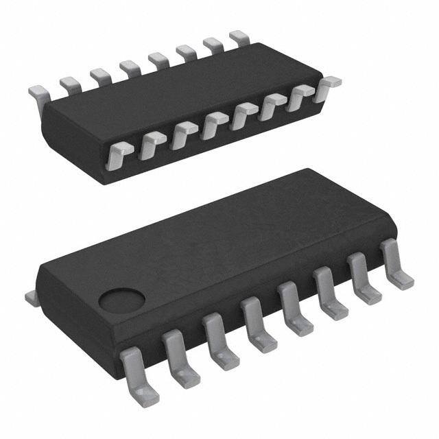
| 描述 | IC LINE RCVR QUAD CMOS 16-SOIC总线接收器 CMOS Quad Diff Line Rcvrs |
| 产品分类 | |
| 品牌 | Texas Instruments |
| 产品手册 | |
| 产品图片 |
|
| rohs | 否含铅 / 不符合限制有害物质指令(RoHS)规范要求 |
| 产品系列 | 逻辑集成电路,总线接收器,Texas Instruments DS26C32ATM- |
| 数据手册 | |
| 产品型号 | DS26C32ATM |
| 产品种类 | 总线接收器 |
| 供应商器件封装 | 16-SOIC N |
| 包装 | 管件 |
| 协议 | RS422,RS423 |
| 双工 | - |
| 商标 | Texas Instruments |
| 安装类型 | 表面贴装 |
| 安装风格 | SMD/SMT |
| 封装 | Tube |
| 封装/外壳 | 16-SOIC(0.154",3.90mm 宽) |
| 封装/箱体 | SOIC-16 Narrow |
| 工作温度 | -40°C ~ 85°C |
| 工作电源电压 | 5 V |
| 工厂包装数量 | 48 |
| 接口类型 | EIA-422, EIA-423, RS-422, RS-423 |
| 接收器滞后 | 60mV |
| 接收机信号类型 | Differential |
| 接收机数量 | 4 |
| 数据速率 | - |
| 最大工作温度 | + 85 C |
| 最小工作温度 | - 40 C |
| 标准包装 | 48 |
| 电压-电源 | 4.5 V ~ 5.5 V |
| 类型 | 接收器 |
| 系列 | DS26C32AT |
| 驱动器/接收器数 | 0/4 |


- 商务部:美国ITC正式对集成电路等产品启动337调查
- 曝三星4nm工艺存在良率问题 高通将骁龙8 Gen1或转产台积电
- 太阳诱电将投资9.5亿元在常州建新厂生产MLCC 预计2023年完工
- 英特尔发布欧洲新工厂建设计划 深化IDM 2.0 战略
- 台积电先进制程称霸业界 有大客户加持明年业绩稳了
- 达到5530亿美元!SIA预计今年全球半导体销售额将创下新高
- 英特尔拟将自动驾驶子公司Mobileye上市 估值或超500亿美元
- 三星加码芯片和SET,合并消费电子和移动部门,撤换高东真等 CEO
- 三星电子宣布重大人事变动 还合并消费电子和移动部门
- 海关总署:前11个月进口集成电路产品价值2.52万亿元 增长14.8%


PDF Datasheet 数据手册内容提取
DS26C32AM, DS26C32AT www.ti.com SNLS382C–JUNE1998–REVISEDAPRIL2013 DS26C32AT/DS26C32AM Quad Differential Line Receiver CheckforSamples:DS26C32AM,DS26C32AT FEATURES DESCRIPTION 1 • CMOSDesignforLowPower The DS26C32A is a quad differential line receiver 2 designed to meet the RS-422, RS-423, and Federal • ±0.2VSensitivityoverInputCommonMode Standards 1020 and 1030 for balanced and VoltageRange unbalanced digital data transmission, while retaining • TypicalPropagationDelays:19ns thelowpowercharacteristicsofCMOS. • TypicalInputhysteresis:60mV The DS26C32A has an input sensitivity of 200 mV • InputsWon'tLoadLineWhenV =0V over the common mode input voltage range of ±7V. CC The DS26C32A features internal pull-up and pull- • MeetstheRequirementsofEIAStandardRS- down resistors which prevent output oscillation on 422 unusedchannels. • TRI-STATEOutputsforConnectiontoSystem The DS26C32A provides an enable and disable Buses function common to all four receivers. It also features • AvailableinSurfaceMount TRI-STATE outputs with 6 mA source and sink • Mil-Std-883CCompliant capability. This product is pin compatible with the DS26LS32AandtheAM26LS32. LogicDiagram 1 Pleasebeawarethatanimportantnoticeconcerningavailability,standardwarranty,anduseincriticalapplicationsof TexasInstrumentssemiconductorproductsanddisclaimerstheretoappearsattheendofthisdatasheet. Alltrademarksarethepropertyoftheirrespectiveowners. 2 PRODUCTIONDATAinformationiscurrentasofpublicationdate. Copyright©1998–2013,TexasInstrumentsIncorporated Products conform to specifications per the terms of the Texas Instruments standard warranty. Production processing does not necessarilyincludetestingofallparameters.
DS26C32AM, DS26C32AT SNLS382C–JUNE1998–REVISEDAPRIL2013 www.ti.com Connection Diagrams TopView ForCompleteMilitaryProductSpecifications,refertotheappropriateSMDorMDS. Figure1. PDIPPackage SeePackageNumberD0016AorNFG0016E SeePackageNumberNAJ0020A,NFE0016AorNAD0016A TopView Figure2. 20-LeadCeramicLeadlessChipCarrier LCCCPackage Thesedeviceshavelimitedbuilt-inESDprotection.Theleadsshouldbeshortedtogetherorthedeviceplacedinconductivefoam duringstorageorhandlingtopreventelectrostaticdamagetotheMOSgates. 2 SubmitDocumentationFeedback Copyright©1998–2013,TexasInstrumentsIncorporated ProductFolderLinks:DS26C32AM DS26C32AT
DS26C32AM, DS26C32AT www.ti.com SNLS382C–JUNE1998–REVISEDAPRIL2013 Absolute Maximum Ratings(1)(2)(3) SupplyVoltage(V ) 7V CC CommonModeRange(V ) ±14V CM DifferentialInputVoltage(V ) ±14V DIFF EnableInputVoltage(V ) 7V IN StorageTemperatureRange(T ) −65°Cto+150°C STG LeadTemperature(Soldering4sec.) 260°C MaximumPowerDissipationat25°C (4) CeramicNFE0016APackage 2308mW PlasticNFG0016EPackage 1645mW SOICD0016APackage 1190mW CeramicNAJ0020APackage 2108mW CeramicNAD0016APackage 1215mW MaximumCurrentPerOutput ±25mA Thisdevicedoesnotmeet2000VESDrating.(5) (1) AbsoluteMaximumRatingsarethosevaluesbeyondwhichthesafetyofthedevicecannotbeensured.Theyarenotmeanttoimplythat thedeviceshouldbeoperatedattheselimits.Thetableof“ElectricalCharacteristics”providesconditionsforactualdeviceoperation. (2) Unlessotherwisespecified,allvoltagesarereferencedtoground. (3) IfMilitary/Aerospacespecifieddevicesarerequired,pleasecontacttheTISalesOffice/Distributorsforavailabilityandspecifications (4) Ratingsapplytoambienttemperatureat25°C.AbovethistemperaturederateNPackage13.16mW/°C,JPackage15.38mW/°C,M Package9.52mW/°C,EPackage12.04mW/°C,andWpackage6.94mW/°C. (5) ESDRating:HBM(1.5kΩ,100pF) Inputs≥2000V Allotherpins≥1000V EIAJ(0Ω,200pF)≥350V Operating Conditions Min Max Units SupplyVoltage(V ) 4.50 5.50 V CC OperatingTemperatureRange(T ) A DS26C32AT −40 +85 °C DS26C32AM −55 +125 °C EnableInputRiseorFallTimes 500 ns DC Electrical Characteristics V =5V±10%(unlessotherwisespecified)(1) CC Parameter TestConditions Min Typ Max Units V MinimumDifferential V =V orV −200 35 +200 mV TH OUT OH OL InputVoltage −7V<V <+7V CM R InputResistance V =−7V,+7V DS26C32AT 5.0 6.8 10 kΩ IN IN (OtherInput=GND) DS26C32AM 4.5 6.8 11 kΩ I InputCurrent V =+10V, DS26C32AT +1.1 +1.5 mA IN IN OtherInput=GND DS26C32AM +1.1 +1.8 mA V =−10V, DS26C32AT −2.0 −2.5 mA IN OtherInput=GND DS26C32AM −2.0 −2.7 mA V MinimumHighLevel V =Min,V =+1V 3.8 4.2 V OH CC DIFF OutputVoltage I =−6.0mA OUT V MaximumLowLevel V =Max,V =−1V 0.2 0.3 V OL CC DIFF OutputVoltage I =6.0mA OUT V MinimumEnableHigh 2.0 V IH InputLevelVoltage V MaximumEnableLow 0.8 V IL InputLevelVoltage (1) AbsoluteMaximumRatingsarethosevaluesbeyondwhichthesafetyofthedevicecannotbeensured.Theyarenotmeanttoimplythat thedeviceshouldbeoperatedattheselimits.Thetableof“ElectricalCharacteristics”providesconditionsforactualdeviceoperation. Copyright©1998–2013,TexasInstrumentsIncorporated SubmitDocumentationFeedback 3 ProductFolderLinks:DS26C32AM DS26C32AT
DS26C32AM, DS26C32AT SNLS382C–JUNE1998–REVISEDAPRIL2013 www.ti.com DC Electrical Characteristics (continued) V =5V±10%(unlessotherwisespecified)(1) CC Parameter TestConditions Min Typ Max Units I MaximumTRI-STATE V =V orGND, ±0.5 ±5.0 μA OZ OUT CC OutputLeakageCurrent ENABLE=V , IL ENABLE=V IH I MaximumEnableInput V =V orGND ±1.0 μA I IN CC Current I QuiescentPower V =Max, DS26C32AT 16 23 mA CC CC SupplyCurrent V =+1V DS26C32AM 16 25 mA DIF V InputHysteresis V =0V 60 mV HYST CM AC Electrical Characteristics V =5V±10% (1) CC Max Parameter TestConditions Min Typ Units DS26C32AT DS26C32AM t , PropagationDelay C =50pF 10 19 30 35 ns PLH L t InputtoOutput PHL V =2.5V DIFF V =0V CM t , OutputRiseand C =50pF 4 9 9 ns RISE L t FallTimes FALL V =2.5V DIFF V =0V CM t , PropagationDelay C =50pF 13 22 29 ns PLZ L t ENABLEtoOutput PHZ R =1000Ω L V =2.5V DIFF t , PropagationDelay C =50pF 13 23 29 ns PZL L t ENABLEtoOutput PZH R =1000Ω L V =2.5V DIFF (1) Unlessotherwisespecified,Min/Maxlimitsapplyoverrecommendedoperatingconditions.AlltypicalsaregivenforV =5VandT = CC A 25°C. Comparison Table of Switching Characteristics into “LS-Type” Load (Figure6,Figure7,andFigure8) (1) DS26C32A DS26LS32A Parameter TestConditions Units Typ Typ t InputtoOutput C =15pF 17 23 ns PLH L t 19 23 ns PHL t ENABLEtoOutput C =5pF 13 15 ns LZ L t 12 20 ns HZ t ENABLEtoOutput C =15pF 13 14 ns ZL L t 13 15 ns ZH (1) Thistableisprovidedforcomparisonpurposesonly.ThevaluesinthistablefortheDS26C32Areflecttheperformanceofthedevice, butarenottested. 4 SubmitDocumentationFeedback Copyright©1998–2013,TexasInstrumentsIncorporated ProductFolderLinks:DS26C32AM DS26C32AT
DS26C32AM, DS26C32AT www.ti.com SNLS382C–JUNE1998–REVISEDAPRIL2013 TEST AND SWITCHING WAVEFORMS Figure3. PropagationDelay C includesloadandtestjigcapacitance. L S =V fort ,andt measurements. 1 CC PZL PLZ S =Gndfort andt measurements. 1 PZH PHZ Figure4. TestCircuitforTRI-STATEOutputTests Figure5. TRI-STATEOutputEnableandDisableWaveforms AC Test Circuit and Switching Time Waveforms Figure6. LoadTestCircuitforTRI-STATEOutputsfor“LS-Type”Load Copyright©1998–2013,TexasInstrumentsIncorporated SubmitDocumentationFeedback 5 ProductFolderLinks:DS26C32AM DS26C32AT
DS26C32AM, DS26C32AT SNLS382C–JUNE1998–REVISEDAPRIL2013 www.ti.com Figure7. PropagationDelayfor“LS-Type”Load (1) DiagramshownforENABLElow. (2) S1andS2ofloadcircuitareclosedexceptwhereshown. (3) Pulsegeneratorforallpulses:Rate≤1.0MHz;Z =50Ω;t ≤15ns;t ≤6.0ns. O r f Figure8. EnableandDisableTimesfor“LS-Type”Load Truth Table(1) ENABLE ENABLE Input Output L H X Z AllOther V ≥V (Max) H ID TH Combinationsof V ≤V (Min) L EnableInputs ID TH Open H (1) Z=TRI-STATE TYPICAL APPLICATIONS Figure9. Two-WireBalancedSystems,RS-422 6 SubmitDocumentationFeedback Copyright©1998–2013,TexasInstrumentsIncorporated ProductFolderLinks:DS26C32AM DS26C32AT
DS26C32AM, DS26C32AT www.ti.com SNLS382C–JUNE1998–REVISEDAPRIL2013 Typical Performance Characteristics DifferentialPropagationDelay DifferentialPropagationDelay vsTemperature vsPowerSupplyVoltage Figure10. Figure11. DifferentialSkew vs DifferentialSkewvs Power Temperature SupplyVoltage Figure12. Figure13. OutputHighVoltagevs OutputHighVoltagevs OutputHighCurrent OutputHighCurrent Figure14. Figure15. Copyright©1998–2013,TexasInstrumentsIncorporated SubmitDocumentationFeedback 7 ProductFolderLinks:DS26C32AM DS26C32AT
DS26C32AM, DS26C32AT SNLS382C–JUNE1998–REVISEDAPRIL2013 www.ti.com Typical Performance Characteristics (continued) OutputLowVoltagevs OutputLowVoltagevs OutputLowCurrent OutputLowCurrent Figure16. Figure17. InputCurrent vs InputResistancevs Power InputVoltage SupplyVoltage Figure18. Figure19. Hysteresis&Differential Hysteresis&Differential TransitionVoltagevs TransitionVoltagevs Temperature PowerSupplyVoltage Figure20. Figure21. 8 SubmitDocumentationFeedback Copyright©1998–2013,TexasInstrumentsIncorporated ProductFolderLinks:DS26C32AM DS26C32AT
DS26C32AM, DS26C32AT www.ti.com SNLS382C–JUNE1998–REVISEDAPRIL2013 Typical Performance Characteristics (continued) SupplyCurrentvs DisabledSupplyCurrentvs Temperature PowerSupplyVoltage Figure22. Figure23. SupplyCurrentvs DataRate Figure24. Copyright©1998–2013,TexasInstrumentsIncorporated SubmitDocumentationFeedback 9 ProductFolderLinks:DS26C32AM DS26C32AT
DS26C32AM, DS26C32AT SNLS382C–JUNE1998–REVISEDAPRIL2013 www.ti.com REVISION HISTORY ChangesfromRevisionB(April2013)toRevisionC Page • ChangedlayoutofNationalDataSheettoTIformat............................................................................................................ 9 10 SubmitDocumentationFeedback Copyright©1998–2013,TexasInstrumentsIncorporated ProductFolderLinks:DS26C32AM DS26C32AT
PACKAGE OPTION ADDENDUM www.ti.com 23-Aug-2017 PACKAGING INFORMATION Orderable Device Status Package Type Package Pins Package Eco Plan Lead/Ball Finish MSL Peak Temp Op Temp (°C) Device Marking Samples (1) Drawing Qty (2) (6) (3) (4/5) DS26C32ATM LIFEBUY SOIC D 16 48 TBD Call TI Call TI -40 to 85 DS26C32ATM DS26C32ATM/NOPB ACTIVE SOIC D 16 48 Green (RoHS CU SN Level-1-260C-UNLIM -40 to 85 DS26C32ATM & no Sb/Br) DS26C32ATMX LIFEBUY SOIC D 16 2500 TBD Call TI Call TI -40 to 85 DS26C32ATM DS26C32ATMX/NOPB ACTIVE SOIC D 16 2500 Green (RoHS CU SN Level-1-260C-UNLIM -40 to 85 DS26C32ATM & no Sb/Br) (1) The marketing status values are defined as follows: ACTIVE: Product device recommended for new designs. LIFEBUY: TI has announced that the device will be discontinued, and a lifetime-buy period is in effect. NRND: Not recommended for new designs. Device is in production to support existing customers, but TI does not recommend using this part in a new design. PREVIEW: Device has been announced but is not in production. Samples may or may not be available. OBSOLETE: TI has discontinued the production of the device. (2) RoHS: TI defines "RoHS" to mean semiconductor products that are compliant with the current EU RoHS requirements for all 10 RoHS substances, including the requirement that RoHS substance do not exceed 0.1% by weight in homogeneous materials. Where designed to be soldered at high temperatures, "RoHS" products are suitable for use in specified lead-free processes. TI may reference these types of products as "Pb-Free". RoHS Exempt: TI defines "RoHS Exempt" to mean products that contain lead but are compliant with EU RoHS pursuant to a specific EU RoHS exemption. Green: TI defines "Green" to mean the content of Chlorine (Cl) and Bromine (Br) based flame retardants meet JS709B low halogen requirements of <=1000ppm threshold. Antimony trioxide based flame retardants must also meet the <=1000ppm threshold requirement. (3) MSL, Peak Temp. - The Moisture Sensitivity Level rating according to the JEDEC industry standard classifications, and peak solder temperature. (4) There may be additional marking, which relates to the logo, the lot trace code information, or the environmental category on the device. (5) Multiple Device Markings will be inside parentheses. Only one Device Marking contained in parentheses and separated by a "~" will appear on a device. If a line is indented then it is a continuation of the previous line and the two combined represent the entire Device Marking for that device. (6) Lead/Ball Finish - Orderable Devices may have multiple material finish options. Finish options are separated by a vertical ruled line. Lead/Ball Finish values may wrap to two lines if the finish value exceeds the maximum column width. Important Information and Disclaimer:The information provided on this page represents TI's knowledge and belief as of the date that it is provided. TI bases its knowledge and belief on information provided by third parties, and makes no representation or warranty as to the accuracy of such information. Efforts are underway to better integrate information from third parties. TI has taken and continues to take reasonable steps to provide representative and accurate information but may not have conducted destructive testing or chemical analysis on incoming materials and chemicals. TI and TI suppliers consider certain information to be proprietary, and thus CAS numbers and other limited information may not be available for release. Addendum-Page 1
PACKAGE OPTION ADDENDUM www.ti.com 23-Aug-2017 In no event shall TI's liability arising out of such information exceed the total purchase price of the TI part(s) at issue in this document sold by TI to Customer on an annual basis. Addendum-Page 2
PACKAGE MATERIALS INFORMATION www.ti.com 10-Aug-2018 TAPE AND REEL INFORMATION *Alldimensionsarenominal Device Package Package Pins SPQ Reel Reel A0 B0 K0 P1 W Pin1 Type Drawing Diameter Width (mm) (mm) (mm) (mm) (mm) Quadrant (mm) W1(mm) DS26C32ATMX/NOPB SOIC D 16 2500 330.0 16.4 6.5 10.3 2.3 8.0 16.0 Q1 PackMaterials-Page1
PACKAGE MATERIALS INFORMATION www.ti.com 10-Aug-2018 *Alldimensionsarenominal Device PackageType PackageDrawing Pins SPQ Length(mm) Width(mm) Height(mm) DS26C32ATMX/NOPB SOIC D 16 2500 367.0 367.0 35.0 PackMaterials-Page2
None
IMPORTANTNOTICE TexasInstrumentsIncorporated(TI)reservestherighttomakecorrections,enhancements,improvementsandotherchangestoits semiconductorproductsandservicesperJESD46,latestissue,andtodiscontinueanyproductorserviceperJESD48,latestissue.Buyers shouldobtainthelatestrelevantinformationbeforeplacingordersandshouldverifythatsuchinformationiscurrentandcomplete. TI’spublishedtermsofsaleforsemiconductorproducts(http://www.ti.com/sc/docs/stdterms.htm)applytothesaleofpackagedintegrated circuitproductsthatTIhasqualifiedandreleasedtomarket.AdditionaltermsmayapplytotheuseorsaleofothertypesofTIproductsand services. ReproductionofsignificantportionsofTIinformationinTIdatasheetsispermissibleonlyifreproductioniswithoutalterationandis accompaniedbyallassociatedwarranties,conditions,limitations,andnotices.TIisnotresponsibleorliableforsuchreproduced documentation.Informationofthirdpartiesmaybesubjecttoadditionalrestrictions.ResaleofTIproductsorserviceswithstatements differentfromorbeyondtheparametersstatedbyTIforthatproductorservicevoidsallexpressandanyimpliedwarrantiesforthe associatedTIproductorserviceandisanunfairanddeceptivebusinesspractice.TIisnotresponsibleorliableforanysuchstatements. BuyersandotherswhoaredevelopingsystemsthatincorporateTIproducts(collectively,“Designers”)understandandagreethatDesigners remainresponsibleforusingtheirindependentanalysis,evaluationandjudgmentindesigningtheirapplicationsandthatDesignershave fullandexclusiveresponsibilitytoassurethesafetyofDesigners'applicationsandcomplianceoftheirapplications(andofallTIproducts usedinorforDesigners’applications)withallapplicableregulations,lawsandotherapplicablerequirements.Designerrepresentsthat,with respecttotheirapplications,Designerhasallthenecessaryexpertisetocreateandimplementsafeguardsthat(1)anticipatedangerous consequencesoffailures,(2)monitorfailuresandtheirconsequences,and(3)lessenthelikelihoodoffailuresthatmightcauseharmand takeappropriateactions.DesigneragreesthatpriortousingordistributinganyapplicationsthatincludeTIproducts,Designerwill thoroughlytestsuchapplicationsandthefunctionalityofsuchTIproductsasusedinsuchapplications. TI’sprovisionoftechnical,applicationorotherdesignadvice,qualitycharacterization,reliabilitydataorotherservicesorinformation, including,butnotlimitedto,referencedesignsandmaterialsrelatingtoevaluationmodules,(collectively,“TIResources”)areintendedto assistdesignerswhoaredevelopingapplicationsthatincorporateTIproducts;bydownloading,accessingorusingTIResourcesinany way,Designer(individuallyor,ifDesignerisactingonbehalfofacompany,Designer’scompany)agreestouseanyparticularTIResource solelyforthispurposeandsubjecttothetermsofthisNotice. TI’sprovisionofTIResourcesdoesnotexpandorotherwisealterTI’sapplicablepublishedwarrantiesorwarrantydisclaimersforTI products,andnoadditionalobligationsorliabilitiesarisefromTIprovidingsuchTIResources.TIreservestherighttomakecorrections, enhancements,improvementsandotherchangestoitsTIResources.TIhasnotconductedanytestingotherthanthatspecifically describedinthepublisheddocumentationforaparticularTIResource. Designerisauthorizedtouse,copyandmodifyanyindividualTIResourceonlyinconnectionwiththedevelopmentofapplicationsthat includetheTIproduct(s)identifiedinsuchTIResource.NOOTHERLICENSE,EXPRESSORIMPLIED,BYESTOPPELOROTHERWISE TOANYOTHERTIINTELLECTUALPROPERTYRIGHT,ANDNOLICENSETOANYTECHNOLOGYORINTELLECTUALPROPERTY RIGHTOFTIORANYTHIRDPARTYISGRANTEDHEREIN,includingbutnotlimitedtoanypatentright,copyright,maskworkright,or otherintellectualpropertyrightrelatingtoanycombination,machine,orprocessinwhichTIproductsorservicesareused.Information regardingorreferencingthird-partyproductsorservicesdoesnotconstitutealicensetousesuchproductsorservices,orawarrantyor endorsementthereof.UseofTIResourcesmayrequirealicensefromathirdpartyunderthepatentsorotherintellectualpropertyofthe thirdparty,oralicensefromTIunderthepatentsorotherintellectualpropertyofTI. TIRESOURCESAREPROVIDED“ASIS”ANDWITHALLFAULTS.TIDISCLAIMSALLOTHERWARRANTIESOR REPRESENTATIONS,EXPRESSORIMPLIED,REGARDINGRESOURCESORUSETHEREOF,INCLUDINGBUTNOTLIMITEDTO ACCURACYORCOMPLETENESS,TITLE,ANYEPIDEMICFAILUREWARRANTYANDANYIMPLIEDWARRANTIESOF MERCHANTABILITY,FITNESSFORAPARTICULARPURPOSE,ANDNON-INFRINGEMENTOFANYTHIRDPARTYINTELLECTUAL PROPERTYRIGHTS.TISHALLNOTBELIABLEFORANDSHALLNOTDEFENDORINDEMNIFYDESIGNERAGAINSTANYCLAIM, INCLUDINGBUTNOTLIMITEDTOANYINFRINGEMENTCLAIMTHATRELATESTOORISBASEDONANYCOMBINATIONOF PRODUCTSEVENIFDESCRIBEDINTIRESOURCESOROTHERWISE.INNOEVENTSHALLTIBELIABLEFORANYACTUAL, DIRECT,SPECIAL,COLLATERAL,INDIRECT,PUNITIVE,INCIDENTAL,CONSEQUENTIALOREXEMPLARYDAMAGESIN CONNECTIONWITHORARISINGOUTOFTIRESOURCESORUSETHEREOF,ANDREGARDLESSOFWHETHERTIHASBEEN ADVISEDOFTHEPOSSIBILITYOFSUCHDAMAGES. UnlessTIhasexplicitlydesignatedanindividualproductasmeetingtherequirementsofaparticularindustrystandard(e.g.,ISO/TS16949 andISO26262),TIisnotresponsibleforanyfailuretomeetsuchindustrystandardrequirements. WhereTIspecificallypromotesproductsasfacilitatingfunctionalsafetyorascompliantwithindustryfunctionalsafetystandards,such productsareintendedtohelpenablecustomerstodesignandcreatetheirownapplicationsthatmeetapplicablefunctionalsafetystandards andrequirements.Usingproductsinanapplicationdoesnotbyitselfestablishanysafetyfeaturesintheapplication.Designersmust ensurecompliancewithsafety-relatedrequirementsandstandardsapplicabletotheirapplications.DesignermaynotuseanyTIproductsin life-criticalmedicalequipmentunlessauthorizedofficersofthepartieshaveexecutedaspecialcontractspecificallygoverningsuchuse. Life-criticalmedicalequipmentismedicalequipmentwherefailureofsuchequipmentwouldcauseseriousbodilyinjuryordeath(e.g.,life support,pacemakers,defibrillators,heartpumps,neurostimulators,andimplantables).Suchequipmentincludes,withoutlimitation,all medicaldevicesidentifiedbytheU.S.FoodandDrugAdministrationasClassIIIdevicesandequivalentclassificationsoutsidetheU.S. TImayexpresslydesignatecertainproductsascompletingaparticularqualification(e.g.,Q100,MilitaryGrade,orEnhancedProduct). Designersagreethatithasthenecessaryexpertisetoselecttheproductwiththeappropriatequalificationdesignationfortheirapplications andthatproperproductselectionisatDesigners’ownrisk.Designersaresolelyresponsibleforcompliancewithalllegalandregulatory requirementsinconnectionwithsuchselection. DesignerwillfullyindemnifyTIanditsrepresentativesagainstanydamages,costs,losses,and/orliabilitiesarisingoutofDesigner’snon- compliancewiththetermsandprovisionsofthisNotice. MailingAddress:TexasInstruments,PostOfficeBox655303,Dallas,Texas75265 Copyright©2018,TexasInstrumentsIncorporated