
 Datasheet下载
- 型号: DS2155LN+
- 制造商: Maxim
- 库位|库存: xxxx|xxxx
- 要求:
| 数量阶梯 | 香港交货 | 国内含税 |
| +xxxx | $xxxx | ¥xxxx |
查看当月历史价格
查看今年历史价格
DS2155LN+产品简介:
ICGOO电子元器件商城为您提供DS2155LN+由Maxim设计生产,在icgoo商城现货销售,并且可以通过原厂、代理商等渠道进行代购。 DS2155LN+价格参考。MaximDS2155LN+封装/规格:接口 - 电信, Telecom IC Single-Chip Transceiver 100-LQFP (14x14)。您可以下载DS2155LN+参考资料、Datasheet数据手册功能说明书,资料中有DS2155LN+ 详细功能的应用电路图电压和使用方法及教程。
Maxim Integrated的DS2155LN+是一款属于接口 - 电信分类的集成电路(IC),主要用于电信系统中的数据传输和信号处理。以下是其主要应用场景:

 1. 数字信号复用与解复用
   DS2155LN+支持T1/E1/J1通信标准,能够实现多路信号的复用和解复用功能。它适用于需要将多个低速数据流合并为一个高速数据流的场景,例如:
   - 远程接入设备
   - 数字用户线路(DSL)接入复用器(DAM)
   - 小型化网络终端单元

 2. 时钟恢复与信号再生
   在长距离传输过程中,信号可能会受到衰减或失真影响。DS2155LN+具备时钟恢复功能,可以重新生成清晰的时钟信号,并对数据进行整形和再生,从而提高信号质量。这在以下场景中尤为重要:
   - 中继器设计
   - 网络扩展器
   - 数据链路层设备

 3. 点对点通信
   DS2155LN+可用于构建点对点通信链路,特别是在需要兼容T1/E1/J1标准的专用网络中。例如:
   - 工业自动化控制系统的远程通信
   - 铁路信号系统中的数据传输
   - 安防监控系统的实时数据回传

 4. 语音与数据集成
   该芯片支持将语音和数据信号整合到同一信道中传输,适合用于以下应用:
   - 私有分支交换机(PBX)系统
   - 综合业务数字网(ISDN)终端设备
   - 语音网关和IP电话系统

 5. 低功耗与小型化设计
   DS2155LN+具有较低的功耗特性,同时封装紧凑,非常适合便携式或空间受限的电信设备,如:
   - 便携式测试仪器
   - 嵌入式通信模块
   - 物联网(IoT)网关

 总结
DS2155LN+广泛应用于各种电信基础设施和终端设备中,涵盖从传统T1/E1通信到现代混合网络的多种需求。其高性能、低功耗和高可靠性特点,使其成为电信行业中不可或缺的关键组件。
| 参数 | 数值 |
| 产品目录 | 集成电路 (IC)半导体 |
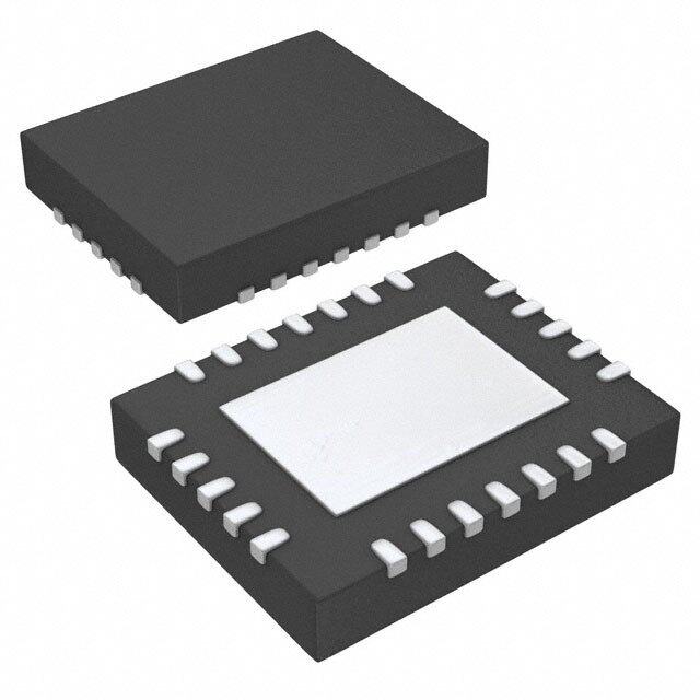
| 描述 | IC TXRX T1/E1/J1 1-CHIP 100-LQFP电信线路管理 IC T1/E1/J1 Transceiver |
| 产品分类 | |
| 品牌 | Maxim Integrated |
| 产品手册 | |
| 产品图片 |
|
| rohs | 符合RoHS无铅 / 符合限制有害物质指令(RoHS)规范要求 |
| 产品系列 | 通信及网络 IC,电信线路管理 IC,Maxim Integrated DS2155LN+- |
| 数据手册 | |
| 产品型号 | DS2155LN+ |
| 产品 | Framer |
| 产品培训模块 | http://www.digikey.cn/PTM/IndividualPTM.page?site=cn&lang=zhs&ptm=25703http://www.digikey.cn/PTM/IndividualPTM.page?site=cn&lang=zhs&ptm=25705 |
| 产品目录页面 | |
| 产品种类 | 电信线路管理 IC |
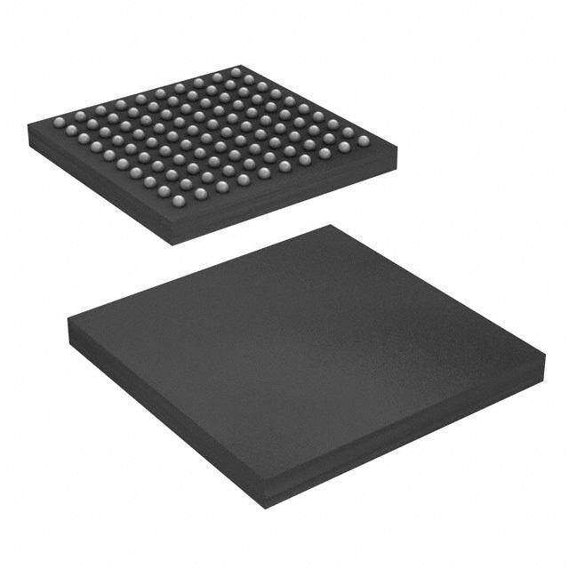
| 供应商器件封装 | 100-LQFP(14x14) |
| 功率(W) | - |
| 功能 | 单芯片收发器 |
| 包括 | BERT 发生器和检测器,CMI 编码器和解码器,HDLC 控制器 |
| 包装 | 管件 |
| 商标 | Maxim Integrated |
| 安装类型 | 表面贴装 |
| 安装风格 | SMD/SMT |
| 封装 | Tube |
| 封装/外壳 | 100-LQFP |
| 封装/箱体 | LQFP-100 |
| 工作温度 | -40°C ~ 85°C |
| 工厂包装数量 | 90 |
| 应用说明 | |
| 接口 | E1,HDLC,J1,T1 |
| 数据速率 | 64 kb/s |
| 最大工作温度 | + 85 C |
| 最小工作温度 | - 40 C |
| 标准包装 | 90 |
| 电压-电源 | 3.14 V ~ 3.47 V |
| 电流-电源 | 75mA |
| 电源电压-最大 | 3.465 V |
| 电源电压-最小 | 3.135 V |
| 电路数 | 1 |
| 系列 | DS2155LN |
| 零件号别名 | 90-2155L+N00 |


- 商务部:美国ITC正式对集成电路等产品启动337调查
- 曝三星4nm工艺存在良率问题 高通将骁龙8 Gen1或转产台积电
- 太阳诱电将投资9.5亿元在常州建新厂生产MLCC 预计2023年完工
- 英特尔发布欧洲新工厂建设计划 深化IDM 2.0 战略
- 台积电先进制程称霸业界 有大客户加持明年业绩稳了
- 达到5530亿美元!SIA预计今年全球半导体销售额将创下新高
- 英特尔拟将自动驾驶子公司Mobileye上市 估值或超500亿美元
- 三星加码芯片和SET,合并消费电子和移动部门,撤换高东真等 CEO
- 三星电子宣布重大人事变动 还合并消费电子和移动部门
- 海关总署:前11个月进口集成电路产品价值2.52万亿元 增长14.8%


PDF Datasheet 数据手册内容提取
DS2155 T1/E1 /J1 Single-Chip Transceiver www.maxim-ic.com GENERAL DESCRIPTION FEATURES The DS2155 is a software-selectable T1, E1, or J1 (cid:131) Complete T1/DS1/ISDN-PRI/J1 Transceiver single-chip transceiver (SCT) for short-haul and Functionality long-haul applications. The DS2155 is composed of a (cid:131) Complete E1 (CEPT) PCM-30/ISDN-PRI line interface unit (LIU), framer, HDLC controllers, Transceiver Functionality and a TDM backplane interface, and is controlled by (cid:131) Long-Haul and Short-Haul Line Interface for an 8-bit parallel port configured for Intel or Motorola Clock/Data Recovery and Waveshaping bus operations. The DS2155 is pin and software (cid:131) CMI Coder/Decoder for Optical I/F compatible with the DS2156. (cid:131) Crystal-Less Jitter Attenuator (cid:131) Fully Independent Transmit and Receive The LIU is composed of transmit and receive Functionality interfaces and a jitter attenuator. The transmit (cid:131) Dual HDLC Controllers interface is responsible for generating the necessary (cid:131) Programmable BERT Generator and Detector waveshapes for driving the network and providing (cid:131) Internal Software-Selectable Receive and the correct source impedance depending on the type Transmit-Side Termination Resistors for of media used. T1 waveform generation includes 75Ω/100Ω/120Ω T1 and E1 Interfaces DSX-1 line buildouts as well as CSU line buildouts (cid:131) Dual Two-Frame Elastic-Store Slip Buffers that of -7.5dB, -15dB, and -22.5dB. E1 waveform Connect to Asynchronous Backplanes Up to generation includes G.703 waveshapes for both 75Ω 16.384MHz coax and 120Ω twisted cables. The receive interface (cid:131) 16.384MHz, 8.192MHz, 4.096MHz, or provides network termination and recovers clock and 2.048MHz Clock Output Synthesized to data from the network. Recovered Network Clock Features continued in Section 3. APPLICATIONS T1/E1/J1 Line Cards ORDERING INFORMATION Switches and Routers Add-Drop Multiplexers PART TEMP RANGE PIN-PACKAGE DS2155L 0°C to +70°C 100 LQFP DS2155L+ 0°C to +70°C 100 LQFP DS2155LN -40°C to +85°C 100 LQFP DS2155 DS2155LN+ -40°C to +85°C 100 LQFP T1/E1/J1 T1/E1/J1 BACKPLANE DS2155G 0°C to +70°C 100 CSBGA NETWORK SCT DS2155G+ 0°C to +70°C 100 CSBGA TDM DS2155GN -40°C to +85°C 100 CSBGA DS2155GN -40°C to +85°C 100 CSBGA + Denotes a lead-free/RoHS-compliant package. Note: Some revisions of this device may incorporate deviations from pub lished specifications known as errata. Multiple revisions of any device may be simultaneously available through various sales channels. For info rmation about device errata, click here: www.maxim-ic.com/errata. 1 of 238 REV: 080607
DS2155 1. TABLE OF CONTENTS 1. TABLE OF CONTENTS............................................................................................................................2 1.1 TABLE OF FIGURES........................................................................................................................................6 1.2 TABLE OF TABLES..........................................................................................................................................7 2. DATA SHEET REVISION HISTORY.....................................................................................................8 3. MAIN FEATURES....................................................................................................................................10 3.1 FUNCTIONAL DESCRIPTION.........................................................................................................................13 3.2 BLOCK DIAGRAM.........................................................................................................................................15 4. PIN FUNCTION DESCRIPTION...........................................................................................................19 4.1 TRANSMIT SIDE...........................................................................................................................................19 4.2 RECEIVE SIDE..............................................................................................................................................21 4.3 PARALLEL CONTROL PORT PINS.................................................................................................................24 4.4 EXTENDED SYSTEM INFORMATION BUS......................................................................................................25 4.5 USER OUTPUT PORT PINS............................................................................................................................26 4.6 JTAG TEST ACCESS PORT PINS...................................................................................................................27 4.7 LINE INTERFACE PINS..................................................................................................................................28 4.8 SUPPLY PINS................................................................................................................................................29 4.9 L AND G PACKAGE PINOUT.........................................................................................................................30 4.10 10MM CSBGA PIN CONFIGURATION......................................................................................................32 5. PARALLEL PORT...................................................................................................................................33 5.1 REGISTER MAP............................................................................................................................................33 6. PROGRAMMING MODEL.....................................................................................................................39 6.1 POWER-UP SEQUENCE.................................................................................................................................40 6.1.1 Master Mode Register.........................................................................................................................40 6.2 INTERRUPT HANDLING................................................................................................................................41 6.3 STATUS REGISTERS......................................................................................................................................41 6.4 INFORMATION REGISTERS...........................................................................................................................42 6.5 INTERRUPT INFORMATION REGISTERS........................................................................................................42 7. SPECIAL PER-CHANNEL REGISTER OPERATION.......................................................................43 8. CLOCK MAP............................................................................................................................................45 9. T1 FRAMER/FORMATTER CONTROL AND STATUS REGISTERS............................................46 9.1 T1 CONTROL REGISTERS.............................................................................................................................46 9.2 T1 TRANSMIT TRANSPARENCY...................................................................................................................51 9.3 AIS-CI AND RAI-CI GENERATION AND DETECTION..................................................................................51 9.4 T1 RECEIVE-SIDE DIGITAL-MILLIWATT CODE GENERATION.....................................................................52 10. E1 FRAMER/FORMATTER CONTROL AND STATUS REGISTERS............................................55 10.1 E1 CONTROL REGISTERS.........................................................................................................................55 10.2 AUTOMATIC ALARM GENERATION.........................................................................................................59 10.3 E1 INFORMATION REGISTERS..................................................................................................................60 11. COMMON CONTROL AND STATUS REGISTERS..........................................................................62 11.1 T1/E1 STATUS REGISTERS......................................................................................................................63 2 of 238
DS2155 12. I/O PIN CONFIGURATION OPTIONS.................................................................................................69 13. LOOPBACK CONFIGURATION..........................................................................................................71 13.1 PER-CHANNEL LOOPBACK......................................................................................................................73 14. ERROR COUNT REGISTERS...............................................................................................................75 14.1 LINE-CODE VIOLATION COUNT REGISTER (LCVCR).............................................................................76 14.1.1 T1 Operation.......................................................................................................................................76 14.1.2 E1 Operation.......................................................................................................................................76 14.2 PATH CODE VIOLATION COUNT REGISTER (PCVCR)............................................................................78 14.2.1 T1 Operation.......................................................................................................................................78 14.2.2 E1 Operation.......................................................................................................................................78 14.3 FRAMES OUT-OF-SYNC COUNT REGISTER (FOSCR)..............................................................................79 14.3.1 T1 Operation.......................................................................................................................................79 14.3.2 E1 Operation.......................................................................................................................................79 14.4 E-BIT COUNTER (EBCR).........................................................................................................................80 15. DS0 MONITORING FUNCTION...........................................................................................................81 16. SIGNALING OPERATION.....................................................................................................................83 16.1 RECEIVE SIGNALING...............................................................................................................................83 16.1.1 Processor-Based Signaling.................................................................................................................83 16.1.2 Hardware-Based Receive Signaling...................................................................................................84 16.2 TRANSMIT SIGNALING.............................................................................................................................89 16.2.1 Processor-Based Mode.......................................................................................................................89 16.2.2 Software Signaling Insertion-Enable Registers, E1 CAS Mode..........................................................93 16.2.3 Software Signaling Insertion-Enable Registers, T1 Mode..................................................................95 16.2.4 Hardware-Based Mode.......................................................................................................................95 17. PER-CHANNEL IDLE CODE GENERATION....................................................................................96 17.1 IDLE-CODE PROGRAMMING EXAMPLES..................................................................................................97 18. CHANNEL BLOCKING REGISTERS................................................................................................101 19. ELASTIC STORES OPERATION........................................................................................................104 19.1 RECEIVE SIDE........................................................................................................................................107 19.1.1 T1 Mode............................................................................................................................................107 19.1.2 E1 Mode............................................................................................................................................107 19.2 TRANSMIT SIDE.....................................................................................................................................107 19.2.1 T1 Mode............................................................................................................................................108 19.2.2 E1 Mode............................................................................................................................................108 19.3 ELASTIC STORES INITIALIZATION.........................................................................................................108 19.4 MINIMUM DELAY MODE.......................................................................................................................108 20. G.706 INTERMEDIATE CRC-4 UPDATING (E1 MODE ONLY)...................................................109 21. T1 BIT-ORIENTED CODE (BOC) CONTROLLER..........................................................................110 21.1 TRANSMIT BOC.....................................................................................................................................110 Transmit a BOC..............................................................................................................................................110 21.2 RECEIVE BOC.......................................................................................................................................110 Receive a BOC.................................................................................................................................................110 22. ADDITIONAL (SA) AND INTERNATIONAL (SI) BIT OPERATION (E1 ONLY)......................113 3 of 238
DS2155 22.1 METHOD 1: HARDWARE SCHEME.........................................................................................................113 22.2 METHOD 2: INTERNAL REGISTER SCHEME BASED ON DOUBLE-FRAME..............................................113 22.3 METHOD 3: INTERNAL REGISTER SCHEME BASED ON CRC4 MULTIFRAME........................................116 23. HDLC CONTROLLERS........................................................................................................................126 23.1 BASIC OPERATION DETAILS..................................................................................................................126 23.2 HDLC CONFIGURATION........................................................................................................................126 23.2.1 FIFO Control....................................................................................................................................130 23.3 HDLC MAPPING....................................................................................................................................131 23.3.1 Receive..............................................................................................................................................131 23.3.2 Transmit............................................................................................................................................133 23.3.3 FIFO Information.............................................................................................................................138 23.3.4 Receive Packet-Bytes Available........................................................................................................138 23.3.5 HDLC FIFOs....................................................................................................................................139 23.4 RECEIVE HDLC CODE EXAMPLE..........................................................................................................140 23.5 LEGACY FDL SUPPORT (T1 MODE)......................................................................................................140 23.5.1 Overview...........................................................................................................................................140 23.5.2 Receive Section.................................................................................................................................140 23.5.3 Transmit Section...............................................................................................................................142 23.6 D4/SLC-96 OPERATION........................................................................................................................142 24. LINE INTERFACE UNIT (LIU)...........................................................................................................143 24.1 LIU OPERATION....................................................................................................................................143 24.2 RECEIVER..............................................................................................................................................143 24.2.1 Receive Level Indicator and Threshold Interrupt.............................................................................144 24.2.2 Receive G.703 Synchronization Signal (E1 Mode)...........................................................................144 24.2.3 Monitor Mode...................................................................................................................................144 24.3 TRANSMITTER.......................................................................................................................................145 24.3.1 Transmit Short-Circuit Detector/Limiter..........................................................................................145 24.3.2 Transmit Open-Circuit Detector.......................................................................................................145 24.3.3 Transmit BPV Error Insertion..........................................................................................................145 24.3.4 Transmit G.703 Synchronization Signal (E1 Mode).........................................................................145 24.4 MCLK PRESCALER...............................................................................................................................146 24.5 JITTER ATTENUATOR.............................................................................................................................146 24.6 CMI (CODE MARK INVERSION) OPTION...............................................................................................146 24.7 LIU CONTROL REGISTERS.....................................................................................................................147 24.8 RECOMMENDED CIRCUITS.....................................................................................................................156 24.9 COMPONENT SPECIFICATIONS...............................................................................................................158 25. PROGRAMMABLE IN-BAND LOOP CODE GENERATION AND DETECTION......................163 26. BERT FUNCTION..................................................................................................................................170 26.1 STATUS..................................................................................................................................................170 26.2 MAPPING...............................................................................................................................................170 26.3 BERT REGISTER DESCRIPTIONS...........................................................................................................172 26.4 BERT REPETITIVE PATTERN SET..........................................................................................................176 26.5 BERT BIT COUNTER.............................................................................................................................177 26.6 BERT ERROR COUNTER........................................................................................................................178 27. PAYLOAD ERROR-INSERTION FUNCTION (T1 MODE ONLY)................................................180 27.1 NUMBER-OF-ERRORS REGISTERS..........................................................................................................182 27.1.1 Number-of-Errors Left Register........................................................................................................183 28. INTERLEAVED PCM BUS OPERATION (IBO)...............................................................................184 4 of 238
DS2155 28.1 CHANNEL INTERLEAVE.........................................................................................................................184 28.2 FRAME INTERLEAVE..............................................................................................................................184 29. EXTENDED SYSTEM INFORMATION BUS (ESIB).......................................................................187 30. PROGRAMMABLE BACKPLANE CLOCK SYNTHESIZER........................................................191 31. FRACTIONAL T1/E1 SUPPORT.........................................................................................................191 32. USER-PROGRAMMABLE OUTPUT PINS........................................................................................193 33. TRANSMIT FLOW DIAGRAMS.........................................................................................................194 34. JTAG BOUNDARY SCAN ARCHITECTURE AND TEST ACCESS PORT.................................199 34.1 DESCRIPTION.........................................................................................................................................199 34.2 INSTRUCTION REGISTER........................................................................................................................202 34.3 TEST REGISTERS....................................................................................................................................204 34.4 BOUNDARY SCAN REGISTER.................................................................................................................204 34.5 BYPASS REGISTER.................................................................................................................................204 34.6 IDENTIFICATION REGISTER....................................................................................................................204 35. FUNCTIONAL TIMING DIAGRAMS.................................................................................................208 35.1 T1 MODE...............................................................................................................................................208 35.2 E1 MODE...............................................................................................................................................213 36. OPERATING PARAMETERS..............................................................................................................222 37. AC TIMING PARAMETERS AND DIAGRAMS...............................................................................224 37.1 MULTIPLEXED BUS AC CHARACTERISTICS..........................................................................................224 37.2 NONMULTIPLEXED BUS AC CHARACTERISTICS...................................................................................227 37.3 RECEIVE-SIDE AC CHARACTERISTICS..................................................................................................230 37.4 BACKPLANE CLOCK TIMING: AC CHARACTERISTICS.........................................................................233 37.5 TRANSMIT AC CHARACTERISTICS........................................................................................................234 38. PACKAGE INFORMATION................................................................................................................237 38.1 100-PIN LQFP (56-G5002-000)............................................................................................................237 38.2 100-BALL CSBGA (56-G6008-001).....................................................................................................238 5 of 238
DS2155 1.1 Table of Figures Figure 3-1. Block Diagram........................................................................................................................................15 Figure 3-2. Receive and Transmit LIU......................................................................................................................16 Figure 3-3. Receive and Transmit Framer/HDLC.....................................................................................................17 Figure 3-4. Backplane Interface................................................................................................................................18 Figure 4-1. 10mm CSBGA Pin Configuration..........................................................................................................32 Figure 6-1. Programming Sequence..........................................................................................................................39 Figure 8-1. Clock Map...............................................................................................................................................45 Figure 16-1. Simplified Diagram of Receive Signaling Path....................................................................................83 Figure 16-2. Simplified Diagram of Transmit Signaling Path...................................................................................89 Figure 20-1. CRC-4 Recalculate Method................................................................................................................109 Figure 24-1. Typical Monitor Application..............................................................................................................144 Figure 24-2. CMI Coding........................................................................................................................................146 Figure 24-3. Software-Selected Termination, Metallic Protection..........................................................................156 Figure 24-4. Software-Selected Termination, Longitudinal Protection...................................................................157 Figure 24-5. E1 Transmit Pulse Template...............................................................................................................159 Figure 24-6. T1 Transmit Pulse Template...............................................................................................................159 Figure 24-7. Jitter Tolerance....................................................................................................................................160 Figure 24-8. Jitter Tolerance (E1 Mode).................................................................................................................160 Figure 24-9. Jitter Attenuation (T1 Mode)..............................................................................................................161 Figure 24-10. Jitter Attenuation (E1 Mode)............................................................................................................161 Figure 24-11. Optional Crystal Connections...........................................................................................................162 Figure 26-1. Simplified Diagram of BERT in Network Direction..........................................................................171 Figure 26-2. Simplified Diagram of BERT in Backplane Direction.......................................................................171 Figure 28-1. IBO Example......................................................................................................................................186 Figure 29-1. ESIB Group of Four DS2155s............................................................................................................187 Figure 33-1. T1 Transmit Flow Diagram................................................................................................................194 Figure 33-2. E1 Transmit Flow Diagram................................................................................................................195 Figure 34-1. JTAG Functional Block Diagram.......................................................................................................199 Figure 34-2. TAP Controller State Diagram............................................................................................................202 Figure 35-1. Receive-Side D4 Timing.....................................................................................................................208 Figure 35-2. Receive-Side ESF Timing...................................................................................................................208 Figure 35-3. Receive-Side Boundary Timing (Elastic Store Disabled)...................................................................209 Figure 35-4. Receive-Side 1.544MHz Boundary Timing (Elastic Store Enabled)..................................................209 Figure 35-5. Receive-Side 2.048MHz Boundary Timing (Elastic Store Enabled)..................................................210 Figure 35-6. Transmit-Side D4 Timing...................................................................................................................210 Figure 35-7. Transmit-Side ESF Timing.................................................................................................................211 Figure 35-8. Transmit-Side Boundary Timing (with Elastic Store Disabled).........................................................211 Figure 35-9. Transmit-Side 1.544MHz Boundary Timing (Elastic Store Enabled)................................................212 Figure 35-10. Transmit-Side 2.048MHz Boundary Timing (Elastic Store Enabled)..............................................212 Figure 35-11. Receive-Side Timing........................................................................................................................213 Figure 35-12. Receive-Side Boundary Timing (with Elastic Store Disabled).........................................................213 Figure 35-13. Receive-Side Boundary Timing, RSYSCLK = 1.544MHz (Elastic Store Enabled)........................214 Figure 35-14. Receive-Side Boundary Timing, RSYSCLK = 2.048MHz (Elastic Store Enabled)........................214 Figure 35-15. Receive IBO Channel Interleave Mode Timing...............................................................................215 Figure 35-16. Receive IBO Frame Interleave Mode Timing...................................................................................216 Figure 35-17. G.802 Timing, E1 Mode Only..........................................................................................................217 Figure 35-18. Transmit-Side Timing.......................................................................................................................217 Figure 35-19. Transmit-Side Boundary Timing (Elastic Store Disabled)...............................................................218 Figure 35-20. Transmit-Side Boundary Timing, TSYSCLK = 1.544MHz (Elastic Store Enabled)......................218 Figure 35-21. Transmit-Side Boundary Timing, TSYSCLK = 2.048MHz (Elastic Store Enabled).......................219 Figure 35-22. Transmit IBO Channel Interleave Mode Timing..............................................................................220 6 of 238
DS2155 Figure 35-23. Transmit IBO Frame Interleave Mode Timing.................................................................................221 Figure 37-1. Intel Multiplexed Bus Read Timing (BTS = 0/MUX = 1)..................................................................225 Figure 37-2. Intel Multiplexed Bus Write Timing (BTS = 0/MUX = 1).................................................................225 Figure 37-3. Motorola Multiplexed Bus Timing (BTS = 1/MUX = 1)...................................................................226 Figure 37-4. Intel Nonmultiplexed Bus Read Timing (BTS = 0/MUX = 0)...........................................................228 Figure 37-5. Intel Nonmultiplexed Bus Write Timing (BTS = 0/MUX = 0)..........................................................228 Figure 37-6. Motorola Nonmultiplexed Bus Read Timing (BTS = 1/MUX = 0)....................................................229 Figure 37-7. Motorola Nonmultiplexed Bus Write Timing (BTS = 1/MUX = 0)...................................................229 Figure 37-8. Receive-Side Timing..........................................................................................................................231 Figure 37-9. Receive-Side Timing, Elastic Store Enabled......................................................................................232 Figure 37-10. Receive Line Interface Timing.........................................................................................................232 Figure 37-11 Receive Timing Delay RCLK to BPCLK.........................................................................................233 Figure 37-12. Transmit-Side Timing.......................................................................................................................235 Figure 37-13. Transmit-Side Timing, Elastic Store Enabled...................................................................................236 Figure 37-14. Transmit Line Interface Timing........................................................................................................236 1.2 Table of Tables Table 4-A. Pin Description Sorted by Pin Number...................................................................................................30 Table 5-A. Register Map Sorted by Address.............................................................................................................33 Table 9-A. T1 Alarm Criteria....................................................................................................................................54 Table 10-A. E1 Sync/Resync Criteria.......................................................................................................................56 Table 10-B. E1 Alarm Criteria..................................................................................................................................61 Table 14-A. T1 Line Code Violation Counting Options...........................................................................................76 Table 14-B. E1 Line-Code Violation Counting Options...........................................................................................76 Table 14-C. T1 Path Code Violation Counting Arrangements..................................................................................78 Table 14-D. T1 Frames Out-of-Sync Counting Arrangements.................................................................................79 Table 16-A. Time Slot Numbering Schemes.............................................................................................................90 Table 17-A. Idle-Code Array Address Mapping.......................................................................................................96 Table 17-B. GRIC and GTIC Functions....................................................................................................................98 Table 19-A. Elastic Store Delay After Initialization...............................................................................................108 Table 23-A. HDLC Controller Registers.................................................................................................................127 Table 24-A. Component List (Software-Selected Termination, Metallic Protection).............................................156 Table 24-B. Component List (Software-Selected Termination, Longitudinal Protection)......................................157 Table 24-C. Transformer Specifications..................................................................................................................158 Table 27-A. Transmit Error-Insertion Setup Sequence...........................................................................................180 Table 27-B. Error Insertion Examples.....................................................................................................................182 Table 34-A. Instruction Codes for IEEE 1149.1 Architecture................................................................................203 Table 34-B. ID Code Structure................................................................................................................................204 Table 34-C. Device ID Codes..................................................................................................................................204 Table 34-D. Boundary Scan Control Bits................................................................................................................205 7 of 238
DS2155 2. DATA SHEET REVISION HISTORY REVISION DESCRIPTION In Section 3: Line Interface and Section 3.1: Functional Description, corrected dB values for E1 and T1 (page 10 and page 13): 080607 E1: 0 to -43dB and 0 to -12dB T1: 0 to -15dB and 0 to -36dB 040907 Added Note 1 (GBD for cold temp) to Absolute Maximum Ratings (Section 36). 041806 Replaced Figure 24-3 and Figure 24-4, added Table 24-A and Table 24-B. 011606 Added lead-free packages to Ordering Information table on page 1. 100903 Add revision history table: The previous version of the DS2155 data sheet (12-06-02) did not incorporate a revision history table and did not describe new features added to B1 revision of the DS2155. THE FOLLOWING WERE INADVERTENTLY REMOVED FROM THE PREVIOUS VERSION OF THE DS2155 DATA SHEET: Add CSBGA package information to Ordering Information table on front page Add CSBGA package thermal characteristics to Operating Parameters section Add Transmit Line Build Out Control register (TLBC) description Add Transmit Line Build Out Control register (TLBC) to Port Map Add Transmit Line Build Out Control register (TLBC) description to LIU TRANSMIT section THE FOLLOWING ARE CORRECTIONS TO ERRORS IN THE PREVIOUS VERSION OF THE DS2155 DATA SHEET: Correct Device ID in Device Identification Register Correct Device ID in JTAG ID Code table Correct minimum value for t in AC CHARACTERISTICS: MULTIPLEXED DHW PARALLEL PORT table. t was changed from 5ns to 0ns DHW Correct minimum value for t in AC CHARACTERISTICS: MULTIPLEXED DDR PARALLEL PORT table. t was changed from unstated to 20ns DDR Corrections to AC CHARACTERISTICS: TRANSMIT SIDE timing table. 1. t , t , t , t , t , t , and t typical values have been restated to reflect various IBO CP CH CL LP LH LL SP modes. 2. t , t t , t minimum values have been changed from 75ns to 20ns. CH CL, LH LL 3. t , t minimum values have been changed from 50ns to 20ns. SP LL 4. t minimum values have been changed from 75ns to 22ns. D3 Corrections to AC CHARACTERISTICS: RECEIVE SIDE timing table. 1. t , t , t , t , t , t , and t typical values have been restated to reflect various IBO CP CH CL LP LH LL SP modes. 2. t , t minimum values have been changed from 75ns to 20ns. CH CL, 3. t , t minimum values have been changed from 50ns to 20ns. SH SL 4. t , t typical values have been added. SH SL 5. t t minimum values have been changed from 50ns to 22ns. D3, D4 Correct Transmit Signaling Registers (E1 Mode, CCS Format) table in Transmit Signaling section 8 of 238
DS2155 REVISION DESCRIPTION The definition of the EGL bit in the LIC1 register has been corrected for both T1 and E1 mode. T1 Mode: EGL = 1 was changed from 15dB to –15dB E1 Mode: EGL = 0 was changed from –10dB to –12dB THE FOLLOWING ARE FORMAT CHANGES AND ADDED OR REMOVED TEXT, TABLES OR DIAGRAMS: Replace X* format for showing active low signals with X Remove redundant statements about “multiport configurations” in Interrupt Handling section Remove BASIC NETWORK CONNECTIONS figure in LINE INTERFACE UNIT section Add “Simplified Diagram of BERT in Network Direction” figure to BERT section Add “Simplified Diagram of BERT in Backplane Direction” figure to BERT section Add Receive Signaling Registers (E1 Mode, CCS Format) table to Receive Signaling section Add GRIC and GTIC function table to IAAR register Changed Table of contents to include table of figures and table of tables. Add note for FASRC bit. Add T1 and E1 Transmit Flow Chart. Added RCLK to BPCLK timing diagram. THE FOLLOWING ARE NEW FEATURES AVAILABLE ON THE DS2155 REV B1 AND ARE EXPLAINED IN THE BODY OF THE DATA SHEET Add FRAS0, TCCS, RCCS and GRSRE bits to Signaling Control Register (SIGCR) Add section on AIS-CI and RAI-CI Generation and Detection Add RAIS-CI status bit to Status Register 4 (SR4) and Interrupt Mask Register 4 (IMR4) Add RAIS-CI status bit to Status Register 4 (SR4) Add TRAI-CI control bit to T1 Common Control Register 1 (TCCR1) Add TAIS-CI control bit to T1 Common Control Register 1 (TCCR1) Add Pseudorandom 2E9-1 pattern to PS0, PS1 and PS2 bit description in Bert Control Register 1 (BCR1) Add BD bit to Information Register 2 (INFO2) Add ILUT status bit to Status Register 1 (SR1) and Interrupt Mask Register 1 (IMR1) Add INTDIS and TMSS bits to Common Control Register 3 (CCR3) 9 of 238
DS2155 3. MAIN FEATURES The DS2155 contains all of the features of the previous generation of Dallas Semiconductor’s T1 and E1 SCTs plus many new features. General (cid:131) Transmitter power-down (cid:131) Programmable output clocks for fractional T1, E1, (cid:131) Transmitter 50mA short-circuit limiter with H0, and H12 applications current-limit-exceeded indication (cid:131) Interleaving PCM bus operation (cid:131) Transmit open-circuit-detected indication (cid:131) 8-bit parallel control port, multiplexed or (cid:131) Line interface function can be completely decoupled from the framer/formatter nonmultiplexed, Intel or Motorola (cid:131) IEEE 1149.1 JTAG-Boundary Scan Clock Synthesizer (cid:131) 3.3V supply with 5V tolerant inputs and outputs (cid:131) Output frequencies include 2.048MHz, 4.096MHz, (cid:131) Pin compatible with DS2156, DS2152/DS2154, 8.192MHz, and 16.384MHz and DS21x5Y SCT family (cid:131) Derived from recovered receive clock (cid:131) Signaling System 7 Support (cid:131) RAI-CI, AIS-CI support Jitter Attenuator (cid:131) 100-pin LQFP (14mm x 14mm) (DS2155L) (cid:131) 32-bit or 128-bit crystal-less jitter attenuator (cid:131) 100-pin CSBGA (10mm x 10mm) (DS2155G) (cid:131) Requires only a 2.048MHz master clock for both (cid:131) 3.3V supply with 5V tolerant inputs and outputs E1 and T1 operation with the option to use (cid:131) Evaluation kits 1.544MHz for T1 operation (cid:131) IEEE 1149.1 JTAG boundary scan (cid:131) Can be placed in either the receive or transmit path (cid:131) Driver source code available from the factory or disabled (cid:131) Limit trip indication Line Interface (cid:131) Requires only a 2.048MHz master clock for both Framer/Formatter E1 and T1 operation with the option to use (cid:131) Fully independent transmit and receive 1.544MHz for T1 operation functionality (cid:131) Fully software configurable (cid:131) Full receive and transmit path transparency (cid:131) Short-haul and long-haul applications (cid:131) T1 framing formats include D4 (SLC-96) and ESF (cid:131) Automatic receive sensitivity adjustments (cid:131) Detailed alarm and status reporting with optional (cid:131) Ranges include 0 to -43dB or 0 to -12dB for E1 interrupt support applications and 0 to -15dB or 0 to -36dB for T1 (cid:131) Large path and line error counters for: applications – T1: BPV, CV, CRC6, and framing bit errors (cid:131) Receive level indication in 2.5dB steps from – E1: BPV, CV, CRC4, E-bit, and frame -42.5dB to -2.5dB alignment errors (cid:131) Internal receive termination option for 75Ω, 100Ω, (cid:131) Timed or manual update modes and 120Ω lines (cid:131) DS1 idle code generation on a per-channel basis in (cid:131) Internal transmit termination option for 75Ω, 100Ω, both transmit and receive paths and 120Ω lines – User-defined (cid:131) Monitor application gain settings of 20dB, 26dB, – Digital milliwatt and 32dB (cid:131) ANSI T1.403-1998 Support (cid:131) G.703 receive synchronization-signal mode (cid:131) RAI-CI detection and generation (cid:131) Flexible transmit waveform generation (cid:131) T1 DSX-1 line buildouts (cid:131) AIS-CI detection and generation (cid:131) T1 CSU line buildouts of -7.5dB, -15dB, and (cid:131) E1ETS 300 011 RAI generation -22.5dB (cid:131) G.965 V5.2 link detect (cid:131) E1 waveforms include G.703 waveshapes for (cid:131) Ability to monitor one DS0 channel in both the both 75Ω coax and 120Ω twisted cables transmit and receive paths (cid:131) AIS generation independent of loopbacks (cid:131) In-band repeating pattern generators and detectors (cid:131) Alternating ones and zeros generation – Three independent generators and detectors (cid:131) Square-wave output – Patterns from 1 to 8 bits or 16 bits in length (cid:131) Open-drain output option (cid:131) RCL, RLOS, RRA, and RAIS alarms interrupt on (cid:131) NRZ format option change-of-state 10 of 238
DS2155 (cid:131) Flexible signaling support Test and Diagnostics – Software or hardware based (cid:131) Programmable on-chip bit error-rate testing – Interrupt generated on change of signaling data (cid:131) Pseudorandom patterns including QRSS – Receive signaling freeze on loss-of-sync, (cid:131) User-defined repetitive patterns carrier loss, or frame slip (cid:131) Daly pattern (cid:131) Addition of hardware pins to indicate carrier loss (cid:131) Error insertion single and continuous and signaling freeze (cid:131) Total bit and errored bit counts (cid:131) Automatic RAI generation to ETS 300 011 (cid:131) Payload error insertion specifications (cid:131) Error insertion in the payload portion of the T1 (cid:131) Access to Sa and Si bits frame in the transmit path (cid:131) Errors can be inserted over the entire frame or (cid:131) Option to extend carrier loss criteria to a 1ms selected channels period as per ETS 300 233 (cid:131) Japanese J1 support (cid:131) Insertion options include continuous and absolute number with selectable insertion rates – Ability to calculate and check CRC6 according (cid:131) F-bit corruption for line testing to the Japanese standard (cid:131) Loopbacks: remote, local, analog, and per-channel – Ability to generate Yellow Alarm according to loopback the Japanese standard Extended System Information Bus TDM Bus (cid:131) Host can read interrupt and alarm status on up to 8 (cid:131) Dual two-frame independent receive and transmit ports with a single bus read elastic stores – Independent control and clocking User-Programmable Output Pins – Controlled slip capability with status (cid:131) Four user-defined output pins for controlling – Minimum delay mode supported external logic (cid:131) 16.384MHz maximum backplane burst rate (cid:131) Supports T1 to CEPT (E1) conversion Control Port (cid:131) Programmable output clocks for fractional T1, E1, (cid:131) 8-bit parallel control port H0, and H12 applications (cid:131) Multiplexed or nonmultiplexed buses (cid:131) Interleaving PCM bus operation (cid:131) Intel or Motorola formats (cid:131) Hardware signaling capability (cid:131) Supports polled or interrupt environments – Receive signaling reinsertion to a backplane (cid:131) Software access to device ID and silicon revision multiframe sync (cid:131) Software reset supported – Availability of signaling in a separate PCM – Automatic clear on power-up data stream (cid:131) Hardware reset pin – Signaling freezing (cid:131) Ability to pass the T1 F-bit position through the elastic stores in the 2.048MHz backplane mode (cid:131) Access to the data streams in between the framer/formatter and the elastic stores (cid:131) User-selectable synthesized clock output HDLC Controllers (cid:131) Two independent HDLC controllers (cid:131) Fast load and unload features for FIFOs (cid:131) SS7 support for FISU transmit and receive (cid:131) Independent 128-byte Rx and Tx buffers with interrupt support (cid:131) Access FDL, Sa, or single/multiple DS0 channels (cid:131) DS0 access includes Nx64 or Nx56 (cid:131) Compatible with polled or interrupt driven environments (cid:131) Bit-oriented code (BOC) support 11 of 238
DS2155 The DS2155 is compliant with the following standards: ANSI: T1.403-1995, T1.231–1993, T1.408 AT&T: TR54016, TR62411 ITU: G.703, G.704, G.706, G.736, G.775, G.823, G.932, I.431, O.151, Q.161 ITU-T: Recommendation I.432–03/93 B-ISDN User-Network Interface—Physical Layer Specification ETSI: ETS 300 011, ETS 300 166, ETS 300 233, CTR12, CTR4 Japanese: JTG.703, JTI.431, JJ-20.11 (CMI Coding Only) 12 of 238
DS2155 3.1 Functional Description The DS2155 is a software-selectable T1, E1, or J1 single-chip transceiver (SCT) for short-haul and long- haul applications. The DS2155 is composed of an LIU, framer, HDLC controllers, and a TDM backplane interface, and is controlled by an 8-bit parallel port configured for Intel or Motorola bus operations. The DS2155 is pin and software compatible with the DS2156. The LIU is composed of transmit and receive interfaces and a jitter attenuator. The transmit interface is responsible for generating the necessary waveshapes for driving the network and providing the correct source impedance depending on the type of media used. T1 waveform generation includes DSX-1 line buildouts as well as CSU line buildouts of -7.5dB, -15dB, and -22.5dB. E1 waveform generation includes G.703 waveshapes for both 75Ω coax and 120Ω twisted cables. The receive interface provides network termination and recovers clock and data from the network. The receive sensitivity adjusts automatically to the incoming signal and can be programmed for 0 to -43dB or 0 to -12dB for E1 applications and 0 to -15dB or 0 to -36dB for T1 applications. The jitter attenuator removes phase jitter from the transmitted or received signal. The crystal-less jitter attenuator requires only a 2.048MHz MCLK for both E1 and T1 applications (with the option of using a 1.544MHz MCLK in T1 applications) and can be placed in either transmit or receive data paths. An additional feature of the LIU is a CMI coder/decoder for interfacing to optical networks. On the transmit side, clock, data, and frame-sync signals are provided to the framer by the backplane interface section. The framer inserts the appropriate synchronization framing patterns, alarm information, calculates and inserts the CRC codes, and provides the B8ZS/HDB3 (zero code suppression) and AMI line coding. The receive-side framer decodes AMI, B8ZS, and HDB3 line coding, synchronizes to the data stream, reports alarm information, counts framing/coding/CRC errors, and provides clock/data and frame-sync signals to the backplane interface section. Both the transmit and receive path have two HDLC controllers. The HDLC controllers transmit and receive data through the framer block. The HDLC controllers can be assigned to any time slot, group of time slots, portion of a time slot or to FDL (T1) or Sa bits (E1). Each controller has 128-byte FIFOs, thus reducing the amount of processor overhead required to manage the flow of data. In addition, built-in support for reducing the processor time is required in SS7 applications. The backplane interface provides a versatile method of sending and receiving data from the host system. Elastic stores provide a method for interfacing to asynchronous systems, converting from a T1/E1 network to a 2.048MHz, 4.096MHz, 8.192MHz, or N x 64kHz system backplane. The elastic stores also manage slip conditions (asynchronous interface). An interleave bus option (IBO) is provided to allow up to eight transceivers to share a high-speed backplane. The parallel port provides access for control and configuration of the DS2155’s features. The extended system information bus (ESIB) function allows up to eight transceivers to be accessed by a single read for interrupt status or other user-selectable alarm status information. Diagnostic capabilities include loopbacks, PRBS pattern generation/detection, and 16-bit loop-up and loop-down code generation and detection. 13 of 238
DS2155 Reader’s Note: This data sheet assumes a particular nomenclature of the T1 operating environment. In each 125µs frame there are 24 8-bit channels plus a framing bit. It is assumed that the framing bit is sent first followed by channel 1. Each channel is made up of eight bits that are numbered 1 to 8. Bit number 1 is the MSB and is transmitted first. Bit number 8 is the LSB and is transmitted last. The term “locked” is used to refer to two clock signals that are phase- or frequency-locked or derived from a common clock (i.e., a 1.544MHz clock can be locked to a 2.048MHz clock if they share the same 8kHz component). Throughout this data sheet, the following abbreviations are used: B8ZS Bipolar with 8 Zero Substitution BOC Bit-Oriented Code CRC Cyclical Redundancy Check D4 Superframe (12 frames per multiframe) Multiframe Structure ESF Extended Superframe (24 frames per multiframe) Multiframe Structure FDL Facility Data Link FPS Framing Pattern Sequence in ESF Fs Signaling Framing Pattern in D4 Ft Terminal Framing Pattern in D4 HDLC High-Level Data Link Control MF Multiframe SLC–96 Subscriber Loop Carrier—96 Channels 14 of 238
DS2155 3.2 Block Diagram Figure 3-1 shows a simplified block diagram featuring the major components of the DS2155. Details are shown in subsequent figures. The block diagram is divided into three functional blocks: LIU, FRAMER, and BACKPLANE INTERFACE. Figure 3-1. Block Diagram CLOCK EXTERNAL ACCESS CLOCK TO RECEIVE SIGNALS ADAPTER HDB3 / B8ZS BACKPLANE RX CK SYNC CK CLOCK SYNTH A MUX A LIU R B SINGALING B O P P E T1/E1/J1NETWORK AL LOOPBACK TER ATTENUAT REMOTE LOO R LOOPBACK ASFLINHRAGDARLAMMCLE IsDNREGT PAYLOAD LOO BINACTCIERKRCPFLUAAITCNEE BACKPLAN TX C T E O JI M ALARM GEN LIU L MUX A R HDLCs F CRC GEN HDB3 / B8ZS LIU EXTERNAL ACCESS FRAMER BACKPLANE TO TRANSMIT SIGNALS INTERFACE JTAG HOST INTERFACE ESIB 15 of 238
DS2155 Figure 3-2. Receive and Transmit LIU MCLK XTALD 8XCLK RPOSO RCLKO RNEGO RNEG RCLK RPOS I I I RCL VCO / PLL MUX 32.768MHz JACLK R RRRITNIGP LINE I/FRECEIVE LOCA OR RECTRAJITTER AT EMOTE L RRRCPNOLEKGS L ENT O TRTITNIPG LINE I/FTRANSM LOOPBAC IVE PATHSMITENUATOR OPBACK TTTPNCOELKGS IT K MUX L T T T T T T IU P C N N C P C OS LK EG EG LK OS I I I O O O 16 of 238
DS2155 Figure 3-3. Receive and Transmit Framer/HDLC REC REC HDLC #1 HDLC #2 128 Byte 128 Byte FIFO FIFO DATA MAPPER MAPPER DATA RPOS P RNEG RECEIVE A RCLK F FRAMER CLOCK YL CLOCK R O A A M SYNC D SYNC ER LO LO SYNC OP SYNC TPOS O B P TRANSMIT A TNEG B CLOCK C CLOCK A FRAMER K TCLK C K DATA MAPPER MAPPER DATA XMIT XMIT HDLC #1 HDLC #2 128 Byte 128 Byte FIFO FIFO 17 of 238
DS2155 Figure 3-4. Backplane Interface Sa BIT/FDL RLINK EXTRACTION RLCLK RSIG SIGNALING RSIGFR BUFFER DATA RSYSCLK ELASTIC RSER CLOCK STORE RCLK RSYNC SYNC RMSYNC RFSYNC RDATA CHANNEL RCHCLK TIMING RCHBLK SYNC TSER SIGNALING Sa/FDL ELASTIC BUFFER TSIG DATA INSERT STORE TSSYNC TSYSCLK CLOCK TSYNC TESO TDATA TLCLK TLINK CHANNEL TCHCLK TIMING TCHBLK TCLK TCLK JACLK MUX 18 of 238
DS2155 4. PIN FUNCTION DESCRIPTION 4.1 Transmit Side Signal Name: TCLK Signal Description: Transmit Clock Signal Type: Input A 1.544MHz (T1) or a 2.048MHz (E1) primary clock. Used to clock data through the transmit-side formatter. TCLK can be internally sourced from MCLK. This is the most flexible method and requires only a single clock signal for both T1 or E1. If internal sourcing is used, then the TCLK pin should be connected low. Signal Name: TSER Signal Description: Transmit Serial Data Signal Type: Input Transmit NRZ serial data. Sampled on the falling edge of TCLK when the transmit-side elastic store is disabled. Sampled on the falling edge of TSYSCLK when the transmit-side elastic store is enabled. Signal Name: TCHCLK Signal Description: Transmit Channel Clock Signal Type: Output A 192kHz (T1) or 256kHz (E1) clock that pulses high during the LSB of each channel. Can also be programmed to output a gated transmit bit clock on a per-channel basis. Synchronous with TCLK when the transmit-side elastic store is disabled. Synchronous with TSYSCLK when the transmit-side elastic store is enabled. Useful for parallel- to-serial conversion of channel data. Signal Name: TCHBLK Signal Description: Transmit Channel Block Signal Type: Output A user-programmable output that can be forced high or low during any of the channels. Synchronous with TCLK when the transmit-side elastic store is disabled. Synchronous with TSYSCLK when the transmit-side elastic store is enabled. Useful for blocking clocks to a serial UART or LAPD controller in applications where not all channels are used such as Fractional T1, Fractional E1, 384kbps (H0), 768kbps, or ISDN–PRI. Also useful for locating individual channels in drop-and-insert applications, for external per-channel loopback, and for per-channel conditioning. Signal Name: TSYSCLK Signal Description: Transmit System Clock Signal Type: Input 1.544MHz, 2.048MHz, 4.096MHz, 8.192MHz, or 16.384MHz clock. Only used when the transmit-side elastic store function is enabled. Should be connected low in applications that do not use the transmit-side elastic store. See Section 28 for details on 4.096MHz, 8.192MHz, and 16.384MHz operation using the IBO. Signal Name: TLCLK Signal Description: Transmit Link Clock Signal Type: Output Demand clock for the transmit link data [TLINK] input. T1 Mode: A 4kHz or 2kHz (ZBTSI) clock. E1 Mode: A 4kHz to 20kHz clock. 19 of 238
DS2155 Signal Name: TLINK Signal Description: Transmit Link Data Signal Type: Input If enabled, this pin is sampled on the falling edge of TCLK for data insertion into either the FDL stream (ESF) or the Fs-bit position (D4), or the Z-bit position (ZBTSI) or any combination of the Sa-bit positions (E1). Signal Name: TSYNC Signal Description: Transmit Sync Signal Type: Input/Output A pulse at this pin establishes either frame or multiframe boundaries for the transmit side. Can be programmed to output either a frame or multiframe pulse. If this pin is set to output pulses at frame boundaries, it can also be set by IOCR1.3 to output double-wide pulses at signaling frames in T1 mode. Signal Name: TSSYNC Signal Description: Transmit System Sync Signal Type: Input Only used when the transmit-side elastic store is enabled. A pulse at this pin establishes either frame or multiframe boundaries for the transmit side. Should be connected low in applications that do not use the transmit-side elastic store. Signal Name: TSIG Signal Description: Transmit Signaling Input Signal Type: Input When enabled, this input samples signaling bits for insertion into outgoing PCM data stream. Sampled on the falling edge of TCLK when the transmit-side elastic store is disabled. Sampled on the falling edge of TSYSCLK when the transmit-side elastic store is enabled. Signal Name: TESO Signal Description: Transmit Elastic Store Data Output Signal Type: Output Updated on the rising edge of TCLK with data out of the transmit-side elastic store whether the elastic store is enabled or not. This pin is normally connected to TDATA. Signal Name: TDATA Signal Description: Transmit Data Signal Type: Input Sampled on the falling edge of TCLK with data to be clocked through the transmit-side formatter. This pin is normally connected to TESO. Signal Name: TPOSO Signal Description: Transmit Positive-Data Output Signal Type: Output Updated on the rising edge of TCLKO with the bipolar data out of the transmit-side formatter. Can be programmed to source NRZ data by the output data format (IOCR1.0) control bit. This pin is normally connected to TPOSI. Signal Name: TNEGO Signal Description: Transmit Negative-Data Output Signal Type: Output Updated on the rising edge of TCLKO with the bipolar data out of the transmit-side formatter. This pin is normally connected to TNEGI. Signal Name: TCLKO 20 of 238
DS2155 Signal Description: Transmit Clock Output Signal Type: Output Buffered clock that is used to clock data through the transmit-side formatter (i.e., either TCLK or RCLKI). This pin is normally connected to TCLKI. Signal Name: TPOSI Signal Description: Transmit Positive-Data Input Signal Type: Input Sampled on the falling edge of TCLKI for data to be transmitted out onto the T1 line. Can be internally connected to TPOSO by connecting the LIUC pin high. TPOSI and TNEGI can be connected together in NRZ applications. Signal Name: TNEGI Signal Description: Transmit Negative-Data Input Signal Type: Input Sampled on the falling edge of TCLKI for data to be transmitted out onto the T1 line. Can be internally connected to TNEGO by connecting the LIUC pin high. TPOSI and TNEGI can be connected together in NRZ applications. Signal Name: TCLKI Signal Description: Transmit Clock Input Signal Type: Input Line interface transmit clock. Can be internally connected to TCLKO by connecting the LIUC pin high. 4.2 Receive Side Signal Name: RLINK Signal Description: Receive Link Data Signal Type: Output T1 Mode: Updated with either FDL data (ESF) or Fs bits (D4) or Z bits (ZBTSI) one RCLK before the start of a frame. E1 Mode: Updated with the full E1 data stream on the rising edge of RCLK. Signal Name: RLCLK Signal Description: Receive Link Clock Signal Type: Output T1 Mode: A 4kHz or 2kHz (ZBTSI) clock for the RLINK output. E1 Mode: A 4kHz to 20kHz clock. Signal Name: RCLK Signal Description: Receive Clock Signal Type: Output 1.544MHz (T1) or 2.048MHz (E1) clock that is used to clock data through the receive-side framer. Signal Name: RCHCLK Signal Description: Receive Channel Clock Signal Type: Output A 192kHz (T1) or 256kHz (E1) clock that pulses high during the LSB of each channel. Synchronous with RCLK when the receive-side elastic store is disabled. Synchronous with RSYSCLK when the receive-side elastic store is enabled. Useful for parallel-to-serial conversion of channel data. 21 of 238
DS2155 Signal Name: RCHBLK Signal Description: Receive Channel Block Signal Type: Output A user-programmable output that can be forced high or low during any of the 24 T1 or 32 E1 channels. Synchronous with RCLK when the receive-side elastic store is disabled. Synchronous with RSYSCLK when the receive-side elastic store is enabled. Useful for blocking clocks to a serial UART or LAPD controller in applications where not all channels are used such as fractional service, 384kbps service, 768kbps, or ISDN–PRI. Also useful for locating individual channels in drop-and-insert applications, for external per-channel loopback, and for per-channel conditioning. See Section 18 for details. Signal Name: RSER Signal Description: Receive Serial Data Signal Type: Output Received NRZ serial data. Updated on rising edges of RCLK when the receive-side elastic store is disabled. Updated on the rising edges of RSYSCLK when the receive-side elastic store is enabled. Signal Name: RSYNC Signal Description: Receive Sync Signal Type: Input/Output An extracted pulse, one RCLK wide, is output at this pin that identifies either frame (IOCR1.5 = 0) or multiframe (IOCR1.5 = 1) boundaries. If set to output frame boundaries, then through IOCR1.6, RSYNC can also be set to output double-wide pulses on signaling frames in T1 mode. If the receive-side elastic store is enabled, then this pin can be enabled to be an input through IOCR1.4, at which a frame or multiframe boundary pulse is applied. Signal Name: RFSYNC Signal Description: Receive Frame Sync Signal Type: Output An extracted 8kHz pulse, one RCLK wide, is output at this pin that identifies frame boundaries. Signal Name: RMSYNC Signal Description: Receive Multiframe Sync Signal Type: Output An extracted pulse, one RCLK wide (elastic store disabled) or one RSYSCLK wide (elastic store enabled), is output at this pin that identifies multiframe boundaries. Signal Name: RDATA Signal Description: Receive Data Signal Type: Output Updated on the rising edge of RCLK with the data out of the receive-side framer. Signal Name: RSYSCLK Signal Description: Receive System Clock Signal Type: Input 1.544MHz, 2.048MHz, 4.096MHz, or 8.192MHz clock. Only used when the receive-side elastic store function is enabled. Should be connected low in applications that do not use the receive-side elastic store. See Section 28 for details on 4.096MHz and 8.192MHz operation using the IBO. Signal Name: RSIG Signal Description: Receive Signaling Output Signal Type: Output Outputs signaling bits in a PCM format. Updated on rising edges of RCLK when the receive-side elastic store is disabled. Updated on the rising edges of RSYSCLK when the receive-side elastic store is enabled. 22 of 238
DS2155 Signal Name: RLOS/LOTC Signal Description: Receive Loss-of-Sync/Loss-of-Transmit Clock Signal Type: Output A dual function output that is controlled by the CCR1.0 control bit. This pin can be programmed to either toggle high when the synchronizer is searching for the frame and multiframe or to toggle high if the TCLK pin has not been toggled for 5µs. Signal Name: RCL Signal Description: Receive Carrier Loss Signal Type: Output Set high when the line interface detects a carrier loss. Signal Name: RSIGF Signal Description: Receive Signaling Freeze Signal Type: Output Set high when the signaling data is frozen by either automatic or manual intervention. Used to alert downstream equipment of the condition. Signal Name: BPCLK Signal Description: Backplane Clock Signal Type: Output A user-selectable synthesized clock output that is referenced to the clock that is output at the RCLK pin. Signal Name: RPOSO Signal Description: Receive Positive-Data Output Signal Type: Output Updated on the rising edge of RCLKO with bipolar data out of the line interface. This pin is normally connected to RPOSI. Signal Name: RNEGO Signal Description: Receive Negative-Data Output Signal Type: Output Updated on the rising edge of RCLKO with the bipolar data out of the line interface. This pin is normally connected to RNEGI. Signal Name: RCLKO Signal Description: Receive Clock Output Signal Type: Output Buffered recovered clock from the network. This pin is normally connected to RCLKI. Signal Name: RPOSI Signal Description: Receive Positive-Data Input Signal Type: Input Sampled on the falling edge of RCLKI for data to be clocked through the receive-side framer. RPOSI and RNEGI can be connected together for an NRZ interface. Can be internally connected to RPOSO by connecting the LIUC pin high. Signal Name: RNEGI Signal Description: Receive Negative-Data Input Signal Type: Input Sampled on the falling edge of RCLKI for data to be clocked through the receive-side framer. RPOSI and RNEGI can be connected together for an NRZ interface. Can be internally connected to RNEGO by connecting the LIUC pin high. 23 of 238
DS2155 Signal Name: RCLKI Signal Description: Receive Clock Input Signal Type: Input Clock used to clock data through the receive-side framer. This pin is normally connected to RCLKO. Can be internally connected to RCLKO by connecting the LIUC pin high. 4.3 Parallel Control Port Pins Signal Name: INT Signal Description: Interrupt Signal Type: Output Flags host controller during conditions and events defined in the status registers. Active-low, open-drain output. Signal Name: TSTRST Signal Description: Tri-State Control and Device Reset Signal Type: Input A dual function pin. A 0-to-1 transition issues a hardware reset to the DS2155 register set. A reset clears all configuration registers. Configuration register contents are set to 0. Leaving TSTRST high tri-states all output and I/O pins (including the parallel control port). Set low for normal operation. Useful in board-level testing. Signal Name: MUX Signal Description: Bus Operation Signal Type: Input Set low to select nonmultiplexed bus operation. Set high to select multiplexed bus operation. Signal Name: AD0 to AD7 Signal Description: Data Bus [D0 to D7] or Address/Data Bus Signal Type: Input/Output In nonmultiplexed bus operation (MUX = 0), these serve as the data bus. In multiplexed bus operation (MUX = 1), these pins serve as an 8-bit multiplexed address/data bus. Signal Name: A0 to A6 Signal Description: Address Bus Signal Type: Input In nonmultiplexed bus operation (MUX = 0), these serve as the address bus. In multiplexed bus operation (MUX = 1), these pins are not used and should be connected low. Signal Name: BTS Signal Description: Bus Type Select Signal Type: Input Strap high to select Motorola bus timing; strap low to select Intel bus timing. This pin controls the function of the RD (DS), ALE (AS), and WR (R/W) pins. If BTS = 1, then these pins assume the function listed in parentheses (). Signal Name: RD (DS) Signal Description: Read Input, Data Strobe Signal Type: Input In Intel mode, RD determines when data is read from the device. In Motorola mode, DS is used to write to the device. See Bus Timing Diagrams. 24 of 238
DS2155 Signal Name: CS Signal Description: Chip Select Signal Type: Input Must be low to read or write to the device. CS is an active-low signal. Signal Name: ALE(AS)/A7 Signal Description: Address Latch Enable (Address Strobe) or A7 Signal Type: Input In nonmultiplexed bus operation (MUX = 0), serves as the upper address bit. In multiplexed bus operation (MUX = 1), serves to demultiplex the bus on a positive-going edge. Signal Name: WR (R/W) Signal Description: Write Input(Read/Write) Signal Type: Input WR is an active-low signal. 4.4 Extended System Information Bus Signal Name: ESIBS0 Signal Description: Extended System Information Bus Select 0 Signal Type: Input/Output Used to group two to eight DS2155s into a bus-sharing mode for alarm and status reporting. See Section 29 for more details. Signal Name: ESIBS1 Signal Description: Extended System Information Bus Select 1 Signal Type: Input/Output Used to group two to eight DS2155s into a bus-sharing mode for alarm and status reporting. See Section 29 for more details. Signal Name: ESIBRD Signal Description: Extended System Information Bus Read Signal Type: Input/Output Used to group two to eight DS2155s into a bus-sharing mode for alarm and status reporting. See Section 29 for more details. 25 of 238
DS2155 4.5 User Output Port Pins Signal Name: UOP0 Signal Description: User Output Port 0 Signal Type: Output This output port pin can be set low or high by the CCR4.0 control bit. This pin is forced low on power-up and after any device reset. Signal Name: UOP1 Signal Description: User Output Port 1 Signal Type: Output This output port pin can be set low or high by the CCR4.1 control bit. This pin is forced low on power-up and after any device reset. Signal Name: UOP2 Signal Description: User Output Port 2 Signal Type: Output This output port pin can be set low or high by the CCR4.2 control bit. This pin is forced low on power-up and after any device reset. Signal Name: UOP3 Signal Description: User Output Port 3 Signal Type: Output This output port pin can be set low or high by the CCR4.3 control bit. This pin is forced low on power-up and after any device reset. 26 of 238
DS2155 4.6 JTAG Test Access Port Pins Signal Name: JTRST Signal Description: IEEE 1149.1 Test Reset Signal Type: Input JTRST is used to asynchronously reset the test access port controller. After power-up, JTRST must be toggled from low to high. This action sets the device into the JTAG DEVICE ID mode. Normal device operation is restored by pulling JTRST low. JTRST is pulled high internally by a 10kΩ resistor operation. Signal Name: JTMS Signal Description: IEEE 1149.1 Test Mode Select Signal Type: Input This pin is sampled on the rising edge of JTCLK and is used to place the test access port into the various defined IEEE 1149.1 states. This pin has a 10kΩ pullup resistor. Signal Name: JTCLK Signal Description: IEEE 1149.1 Test Clock Signal Signal Type: Input This signal is used to shift data into JTDI on the rising edge and out of JTDO on the falling edge. Signal Name: JTDI Signal Description: IEEE 1149.1 Test Data Input Signal Type: Input Test instructions and data are clocked into this pin on the rising edge of JTCLK. This pin has a 10kΩ pullup resistor. Signal Name: JTDO Signal Description: IEEE 1149.1 Test Data Output Signal Type: Output Test instructions and data are clocked out of this pin on the falling edge of JTCLK. If not used, this pin should be left unconnected. 27 of 238
DS2155 4.7 Line Interface Pins Signal Name: MCLK Signal Description: Master Clock Input Signal Type: Input A (50ppm) clock source is applied at this pin. This clock is used internally for both clock/data recovery and for the jitter attenuator for T1 and E1 modes. A quartz crystal of 2.048MHz can be applied across MCLK and XTALD instead of the clock source. The clock rate can be 16.384MHz, 8.192MHz, 4.096MHz, or 2.048MHz. When using the DS2155 in T1-only operation, a 1.544MHz (50ppm) clock source can be used. Signal Name: XTALD Signal Description: Quartz Crystal Driver Signal Type: Output A quartz crystal of 2.048MHz (optional 1.544MHz in T1-only operation) can be applied across MCLK and XTALD instead of a clock source at MCLK. Leave open circuited if a clock source is applied at MCLK. Signal Name: 8XCLK Signal Description: Eight Times Clock (8x) Signal Type: Output An 8x clock that is locked to the recovered network clock provided from the clock/data recovery block (if the jitter attenuator is enabled on the receive side) or from the TCLKI pin (if the jitter attenuator is enabled on the transmit side). Signal Name: LIUC Signal Description: Line Interface Connect Signal Type: Input Connect low to separate the line interface circuitry from the framer/formatter circuitry and activate the TPOSI/TNEGI/TCLKI/RPOSI/RNEGI/RCLKI pins. Connect high to connect the line interface circuitry to the framer/formatter circuitry and deactivate the TPOSI/TNEGI/TCLKI/RPOSI/RNEGI/RCLKI pins. When LIUC is connected high, the TPOSI/TNEGI/TCLKI/RPOSI/RNEGI/RCLKI pins should be connected low. Signal Name: RTIP and RRING Signal Description: Receive Tip and Ring Signal Type: Input Analog inputs for clock recovery circuitry. These pins connect through a 1:1 transformer to the network. See Section 24 for details. Signal Name: TTIP and TRING Signal Description: Transmit Tip and Ring Signal Type: Output Analog line driver outputs. These pins connect through a 1:2 step-up transformer to the network. See Section 24 for details. 28 of 238
DS2155 4.8 Supply Pins Signal Name: DVDD Signal Description: Digital Positive Supply Signal Type: Supply 3.3V ±5%. Should be connected to the RVDD and TVDD pins. Signal Name: RVDD Signal Description: Receive Analog Positive Supply Signal Type: Supply 3.3V ±5%. Should be connected to the DVDD and TVDD pins. Signal Name: TVDD Signal Description: Transmit Analog Positive Supply Signal Type: Supply 3.3V ±5%. Should be connected to the RVDD and DVDD pins. Signal Name: DVSS Signal Description: Digital Signal Ground Signal Type: Supply Should be connected to the RVSS and TVSS pins. Signal Name: RVSS Signal Description: Receive Analog Signal Ground Signal Type: Supply 0V. Should be connected to DVSS and TVSS. Signal Name: TVSS Signal Description: Transmit Analog Signal Ground Signal Type: Supply 0V. Should be connected to DVSS and RVSS. 29 of 238
DS2155 4.9 L and G Package Pinout The DS2155 is available in either a 100-pin LQFP (L) or 10mm CSBGA, 0.8mm pitch (G) package. Table 4-A. Pin Description Sorted by Pin Number PIN SYMBOL TYPE FUNCTION LQFP CSBGA 1 A1 RCHBLK O Receive Channel Block 2 B2 JTMS I IEEE 1149.1 Test Mode Select 3 C3 BPCLK O Backplane Clock 4 B1 JTCLK I IEEE 1149.1 Test Clock Signal 5 D4 JTRST I IEEE 1149.1 Test Reset 6 C2 RCL O Receive Carrier Loss 7 C1 JTDI I IEEE 1149.1 Test Data Input 8 D3 UOP0 O User Output 0 9 D2 UOP1 O User Output 1 10 D1 JTDO O IEEE 1149.1 Test Data Output 11 E3 BTS I Bus Type Select 12 E2 LIUC I Line Interface Connect 13 E1 8XCLK O Eight Times Clock 14 E4 TSTRST I Test/Reset 15 E5 UOP2 O User Output 2 16 F1 RTIP I Receive Analog Tip Input 17 F2 RRING I Receive Analog Ring Input 18 F3 RVDD — Receive Analog Positive Supply 19, 20, 24 F4, G1, J1 RVSS — Receive Analog Signal Ground 21 G2 MCLK I Master Clock Input 22 H1 XTALD O Quartz Crystal Driver 23 G3 UOP3 O User Output 3 25 H2 INT O Interrupt 26 K1 N.C. — Reserved for Factory Test 27, 28 J2, H3 N.C. — Reserved for Factory Test 29 K2 TTIP O Transmit Analog Tip Output 30 G4 TVSS – Transmit Analog Signal Ground 31 J3 TVDD – Transmit Analog Positive Supply 32 K3 TRING O Transmit Analog Ring Output 33 H4 TCHBLK O Transmit Channel Block 34 J4 TLCLK O Transmit Link Clock 35 K4 TLINK I Transmit Link Data 36 H5 ESIBS0 I/O Extended System Information Bus 0 37 J5 TSYNC I/O Transmit Sync 38 K5 TPOSI I Transmit Positive-Data Input 39 G5 TNEGI I Transmit Negative-Data Input 40 F5 TCLKI I Transmit Clock Input 41 K6 TCLKO O Transmit Clock Output 42 J6 TNEGO O Transmit Negative-Data Output 43 H6 TPOSO O Transmit Positive-Data Output 44, 61, 81, 83 K7, F8, B8, C7 DVDD — Digital Positive Supply 45, 60, 80, 84 G6, G10, D7, B7 DVSS — Digital Signal Ground 46 J7 TCLK I Transmit Clock 47 K8 TSER I Transmit Serial Data 48 H7 TSIG I Transmit Signaling Input 49 K9 TESO O Transmit Elastic Store Output 50 J8 TDATA I Transmit Data 30 of 238
DS2155 PIN SYMBOL TYPE FUNCTION LQFP CSBGA 51 K10 TSYSCLK I Transmit System Clock 52 J9 TSSYNC I Transmit System Sync 53 H8 TCHCLK O Transmit Channel Clock 54 J10 ESIBS1 I/O Extended System Information Bus 1 55 G7 MUX I Bus Operation 56 H9 D0/AD0 I/O Data Bus Bit0/Address/Data Bus Bit 0 57 H10 D1/AD1 I/O Data Bus Bit1/Address/Data Bus Bit 1 58 G8 D2/AD2 I/O Data Bus Bit 2/Address/Data Bus 2 59 G9 D3/AD3 I/O Data Bus Bit 3/Address/Data Bus Bit 3 62 F9 D4/AD4 I/O Data Bus Bit4/Address/Data Bus Bit 4 63 F10 D5/AD5 I/O Data Bus Bit 5/Address/Data Bus Bit 5 64 F7 D6/AD6 I/O Data Bus Bit 6/Address/Data Bus Bit 6 65 F6 D7/AD7 I/O Data Bus Bit 7/Address/Data Bus Bit 7 66 E10 A0 I Address Bus Bit 0 67 E9 A1 I Address Bus Bit 1 68 E8 A2 I Address Bus Bit 2 69 D10 A3 I Address Bus Bit 3 70 E7 A4 I Address Bus Bit 4 71 D9 A5 I Address Bus Bit 5 72 C10 A6 I Address Bus Bit 6 73 D8 ALE (AS)/A7 I Address Latch Enable/Address Bus Bit 7 74 B10 RD (DS) I Read Input (Data Strobe) 75 C9 CS I Chip Select 76 A10 ESIBRD I/O Extended System Information Bus Read 77 B9 WR (R/W) I Write Input (Read/Write) 78 C8 RLINK O Receive Link Data 79 A9 RLCLK O Receive Link Clock 82 A8 RCLK O Receive Clock 85 A7 RDATA O Receive Data 86 C6 RPOSI I Receive Positive-Data Input 87 B6 RNEGI I Receive Negative-Data Input 88 A6 RCLKI I Receive Clock Input 89 D6 RCLKO O Receive Clock Output 90 E6 RNEGO O Receive Negative-Data Output 91 A5 RPOSO O Receive Positive-Data Output 92 B5 RCHCLK O Receive Channel Clock 93 C5 RSIGF O Receive Signaling-Freeze Output 94 A4 RSIG O Receive Signaling Output 95 D5 RSER O Receive Serial Data 96 B4 RMSYNC O Receive Multiframe Sync 97 A3 RFSYNC O Receive Frame Sync 98 C4 RSYNC I/O Receive Sync 99 A2 RLOS/LOTC O Receive Loss-of-Sync/Loss-of-Transmit Clock 100 B3 RSYSCLK I Receive System Clock 31 of 238
DS2155 4.10 10mm CSBGA Pin Configuration Figure 4-1. 10mm CSBGA Pin Configuration 1 2 3 4 5 6 7 8 9 10 A RLOS/ RCHBLK RFSYNC RSIG RPOSO RCLKI RDATA RCLK RLCLK ESIBRD LOTC B WR RD JTCLK JTMS RSYSCLK RMSYNC RCHCLK RNEGI DVSS DVDD (R/W) (DS) C JTDI RCL BPCLK RSYNC RSIGF RPOSI DVDD RLINK CS A6 D ALE(AS)/ JTDO UOP1 UOP0 JTRST RSER RCLKO DVSS A5 A3 A7 E 8XCLK LIUC BTS TSTRST UOP2 RNEGO A4 A2 A1 A0 F RTIP RRING RVDD RVSS TCLKI D7/AD7 D6/AD6 DVDD D4/AD4 D5/AD5 G RVSS MCLK UOP3 TVSS TNEGI DVSS MUX D2/AD2 D3/AD3 DVSS H XTALD INT N.C. TCHBLK ESIBS0 TPOSO TSIG TCHCLK D0/AD0 D1/AD1 J RVSS N.C. TVDD TLCLK TSYNC TNEGO TCLK TDATA TSSYNC ESIBS1 K TUSEL TTIP TRING TLINK TPOSI TCLKO DVDD TSER TESO TSYSCLK TOP VIEW 32 of 238
DS2155 5. PARALLEL PORT The SCT is controlled by either a nonmultiplexed (MUX = 0) or a multiplexed (MUX = 1) bus through an external microcontroller or microprocessor. The SCT can operate with either Intel or Motorola bus timing configurations. If the BTS pin is connected low, Intel timing is selected; if connected high, Motorola timing is selected. All Motorola bus signals are listed in parentheses (). See the timing diagrams in AC Electrical Characteristics in Section 37 for more details. 5.1 Register Map Table 5-A. Register Map Sorted by Address ADDRESS R/W REGISTER NAME SYMBOL PAGE xxh 00 R/W Master Mode Register MSTRREG 40 01 R/W I/O Configuration Register 1 IOCR1 69 02 R/W I/O Configuration Register 2 IOCR2 70 03 R/W T1 Receive Control Register 1 T1RCR1 46 04 R/W T1 Receive Control Register 2 T1RCR2 47 05 R/W T1 Transmit Control Register 1 T1TCR1 48 06 R/W T1 Transmit Control Register 2 T1TCR2 49 07 R/W T1 Common Control Register 1 T1CCR1 50 08 R/W Software Signaling Insertion Enable 1 SSIE1 93 09 R/W Software Signaling Insertion Enable 2 SSIE2 93 0A R/W Software Signaling Insertion Enable 3 SSIE3 94 0B R/W Software Signaling Insertion Enable 4 SSIE4 94 0C R/W T1 Receive Digital Milliwatt Enable Register 1 T1RDMR1 52 0D R/W T1 Receive Digital Milliwatt Enable Register 2 T1RDMR2 52 0E R/W T1 Receive Digital Milliwatt Enable Register 3 T1RDMR3 52 0F R Device Identification Register IDR 63 10 R/W Information Register 1 INFO1 53 11 R Information Register 2 INFO2 153 12 R/W Information Register 3 INFO3 60 13 — Unused — — 14 R Interrupt Information Register 1 IIR1 42 15 R Interrupt Information Register 2 IIR2 42 16 R/W Status Register 1 SR1 154 17 R/W Interrupt Mask Register 1 IMR1 155 18 R/W Status Register 2 SR2 63 19 R/W Interrupt Mask Register 2 IMR2 64 1A R/W Status Register 3 SR3 65 1B R/W Interrupt Mask Register 3 IMR3 66 1C R/W Status Register 4 SR4 67 1D R/W Interrupt Mask Register 4 IMR4 68 1E R/W Status Register 5 SR5 106 1F R/W Interrupt Mask Register 5 IMR5 106 20 R/W Status Register 6 SR6 135 21 R/W Interrupt Mask Register 6 IMR6 136 22 R/W Status Register 7 SR7 135 23 R/W Interrupt Mask Register 7 IMR7 136 24 R/W Status Register 8 SR8 112 33 of 238
DS2155 ADDRESS R/W REGISTER NAME SYMBOL PAGE xxh 25 R/W Interrupt Mask Register 8 IMR8 112 26 R/W Status Register 9 SR9 174 27 R/W Interrupt Mask Register 9 IMR9 175 28 R/W Per-Channel Pointer Register PCPR 43 29 W Per-Channel Data Register 1 PCDR1 44 2A W Per-Channel Data Register 2 PCDR2 44 2B W Per-Channel Data Register 3 PCDR3 44 2C W Per-Channel Data Register 4 PCDR4 44 2D R/W Information Register 4 INFO4 137 2E R Information Register 5 INFO5 137 2F R Information Register 6 INFO6 137 30 R Information Register 7 INFO7 60 31 R/W HDLC #1 Receive Control H1RC 129 32 R/W HDLC #2 Receive Control H2RC 129 33 R/W E1 Receive Control Register 1 E1RCR1 55 34 R/W E1 Receive Control Register 2 E1RCR2 56 35 R/W E1 Transmit Control Register 1 E1TCR1 57 36 R/W E1 Transmit Control Register 2 E1TCR2 58 37 R/W BOC Control Register BOCC 111 38 R/W Receive Signaling Change-of-State Information 1 RSINFO1 88 39 R/W Receive Signaling Change-of-State Information 2 RSINFO2 88 3A R/W Receive Signaling Change-of-State Information 3 RSINFO3 88 3B R/W Receive Signaling Change-of-State Information 4 RSINFO4 88 3C R/W Receive Signaling Change-of-State Interrupt Enable 1 RSCSE1 88 3D R/W Receive Signaling Change-of-State Interrupt Enable 2 RSCSE2 88 3E R/W Receive Signaling Change-of-State Interrupt Enable 3 RSCSE3 88 3F R/W Receive Signaling Change-of-State Interrupt Enable 4 RSCSE4 88 40 R/W Signaling Control Register SIGCR 85 41 R/W Error Count Configuration Register ERCNT 75 42 R Line Code Violation Count Register 1 LCVCR1 77 43 R Line Code Violation Count Register 2 LCVCR2 77 44 R Path Code Violation Count Register 1 PCVCR1 78 45 R Path Code Violation Count Register 2 PCVCR2 78 46 R Frames Out-of-Sync Count Register 1 FOSCR1 79 47 R Frames Out-of-Sync Count Register 2 FOSCR2 79 48 R E-Bit Count Register 1 EBCR1 80 49 R E-Bit Count Register 2 EBCR2 80 4A R/W Loopback Control Register LBCR 71 4B R/W Per-Channel Loopback Enable Register 1 PCLR1 73 4C R/W Per-Channel Loopback Enable Register 2 PCLR2 73 4D R/W Per-Channel Loopback Enable Register 3 PCLR3 74 4E R/W Per-Channel Loopback Enable Register 4 PCLR4 74 4F R/W Elastic Store Control Register ESCR 105 50 R/W Transmit Signaling Register 1 TS1 91 51 R/W Transmit Signaling Register 2 TS2 91 52 R/W Transmit Signaling Register 3 TS3 91 53 R/W Transmit Signaling Register 4 TS4 91 34 of 238
DS2155 ADDRESS R/W REGISTER NAME SYMBOL PAGE xxh 54 R/W Transmit Signaling Register 5 TS5 91 55 R/W Transmit Signaling Register 6 TS6 91 56 R/W Transmit Signaling Register 7 TS7 91 57 R/W Transmit Signaling Register 8 TS8 91 58 R/W Transmit Signaling Register 9 TS9 91 59 R/W Transmit Signaling Register 10 TS10 91 5A R/W Transmit Signaling Register 11 TS11 91 5B R/W Transmit Signaling Register 12 TS12 91 5C R/W Transmit Signaling Register 13 TS13 91 5D R/W Transmit Signaling Register 14 TS14 91 5E R/W Transmit Signaling Register 15 TS15 91 5F R/W Transmit Signaling Register 16 TS16 91 60 R Receive Signaling Register 1 RS1 86 61 R Receive Signaling Register 2 RS2 86 62 R Receive Signaling Register 3 RS3 86 63 R Receive Signaling Register 4 RS4 86 64 R Receive Signaling Register 5 RS5 86 65 R Receive Signaling Register 6 RS6 86 66 R Receive Signaling Register 7 RS7 86 67 R Receive Signaling Register 8 RS8 86 68 R Receive Signaling Register 9 RS9 86 69 R Receive Signaling Register 10 RS10 86 6A R Receive Signaling Register 11 RS11 86 6B R Receive Signaling Register 12 RS12 86 6C R Receive Signaling Register 13 RS13 86 6D R Receive Signaling Register 14 RS14 86 6E R Receive Signaling Register 15 RS15 86 6F R Receive Signaling Register 16 RS16 86 70 R/W Common Control Register 1 CCR1 62 71 R/W Common Control Register 2 CCR2 191 72 R/W Common Control Register 3 CCR3 192 73 R/W Common Control Register 4 CCR4 149 74 R/W Transmit Channel Monitor Select TDS0SEL 81 75 R Transmit DS0 Monitor Register TDS0M 81 76 R/W Receive Channel Monitor Select RDS0SEL 82 77 R Receive DS0 Monitor Register RDS0M 82 78 R/W Line Interface Control 1 LIC1 147 79 R/W Line Interface Control 2 LIC2 150 7A R/W Line Interface Control 3 LIC3 151 7B R/W Line Interface Control 4 LIC4 152 7C — Unused — — 7D R/W Transmit Line Build-Out Control TLBC 149 7E W Idle Array Address Register IAAR 98 7F R/W Per-Channel Idle Code Value Register PCICR 98 80 R/W Transmit Idle Code Enable Register 1 TCICE1 99 81 R/W Transmit Idle Code Enable Register 2 TCICE2 99 82 R/W Transmit Idle Code Enable Register 3 TCICE3 99 35 of 238
DS2155 ADDRESS R/W REGISTER NAME SYMBOL PAGE xxh 83 R/W Transmit Idle Code Enable Register 4 TCICE4 99 84 R/W Receive Idle Code Enable Register 1 RCICE1 100 85 R/W Receive Idle Code Enable Register 2 RCICE2 100 86 R/W Receive Idle Code Enable Register 3 RCICE3 100 87 R/W Receive Idle Code Enable Register 4 RCICE4 100 88 R/W Receive Channel Blocking Register 1 RCBR1 101 89 R/W Receive Channel Blocking Register 2 RCBR2 101 8A R/W Receive Channel Blocking Register 3 RCBR3 102 8B R/W Receive Channel Blocking Register 4 RCBR4 102 8C R/W Transmit Channel Blocking Register 1 TCBR1 103 8D R/W Transmit Channel Blocking Register 2 TCBR2 103 8E R/W Transmit Channel Blocking Register 3 TCBR3 103 8F R/W Transmit Channel Blocking Register 4 TCBR4 103 90 R/W HDLC #1 Transmit Control H1TC 128 91 R/W HDLC #1 FIFO Control H1FC 130 92 R/W HDLC #1 Receive Channel Select 1 H1RCS1 131 93 R/W HDLC #1 Receive Channel Select 2 H1RCS2 131 94 R/W HDLC #1 Receive Channel Select 3 H1RCS3 131 95 R/W HDLC #1 Receive Channel Select 4 H1RCS4 131 96 R/W HDLC #1 Receive Time Slot Bits/Sa Bits Select H1RTSBS 132 97 R/W HDLC #1 Transmit Channel Select1 H1TCS1 133 98 R/W HDLC #1 Transmit Channel Select2 H1TCS2 133 99 R/W HDLC #1 Transmit Channel Select3 H1TCS3 133 9A R/W HDLC #1 Transmit Channel Select4 H1TCS4 133 9B R/W HDLC #1 Transmit Time Slot Bits/Sa Bits Select H1TTSBS 134 9C R HDLC #1 Receive Packet Bytes Available H1RPBA 138 9D W HDLC #1 Transmit FIFO H1TF 139 9E R HDLC #1 Receive FIFO H1RF 139 9F R HDLC #1 Transmit FIFO Buffer Available H1TFBA 138 A0 R/W HDLC #2 Transmit Control H2TC 128 A1 R/W HDLC #2 FIFO Control H2FC 130 A2 R/W HDLC #2 Receive Channel Select 1 H2RCS1 131 A3 R/W HDLC #2 Receive Channel Select 2 H2RCS2 131 A4 R/W HDLC #2 Receive Channel Select 3 H2RCS3 131 A5 R/W HDLC #2 Receive Channel Select 4 H2RCS4 131 A6 R/W HDLC #2 Receive Time Slot Bits/Sa Bits Select H2RTSBS 132 A7 R/W HDLC #2 Transmit Channel Select1 H2TCS1 133 A8 R/W HDLC #2 Transmit Channel Select2 H2TCS2 133 A9 R/W HDLC #2 Transmit Channel Select3 H2TCS3 133 AA R/W HDLC #2 Transmit Channel Select4 H2TCS4 133 AB R/W HDLC #2 Transmit Time Slot Bits/Sa Bits Select H2TTSBS 134 AC R HDLC #2 Receive Packet Bytes Available H2RPBA 138 AD W HDLC #2 Transmit FIFO H2TF 139 AE R HDLC #2 Receive FIFO H2RF 139 AF R HDLC #2 Transmit FIFO Buffer Available H2TFBA 138 B0 R/W Extend System Information Bus Control Register 1 ESIBCR1 188 B1 R/W Extend System Information Bus Control Register 2 ESIBCR2 189 36 of 238
DS2155 ADDRESS R/W REGISTER NAME SYMBOL PAGE xxh B2 R Extend System Information Bus Register 1 ESIB1 190 B3 R Extend System Information Bus Register 2 ESIB2 190 B4 R Extend System Information Bus Register 3 ESIB3 190 B5 R Extend System Information Bus Register 4 ESIB4 190 B6 R/W In-Band Code Control Register IBCC 164 B7 R/W Transmit Code Definition Register 1 TCD1 165 B8 R/W Transmit Code Definition Register 2 TCD2 165 B9 R/W Receive Up Code Definition Register 1 RUPCD1 166 BA R/W Receive Up Code Definition Register 2 RUPCD2 166 BB R/W Receive Down Code Definition Register 1 RDNCD1 167 BC R/W Receive Down Code Definition Register 2 RDNCD2 167 BD R/W In-Band Receive Spare Control Register RSCC 168 BE R/W Receive Spare Code Definition Register 1 RSCD1 169 BF R/W Receive Spare Code Definition Register 2 RSCD2 169 C0 R Receive FDL Register RFDL 141 C1 R/W Transmit FDL Register TFDL 142 C2 R/W Receive FDL Match Register 1 RFDLM1 141 C3 R/W Receive FDL Match Register 2 RFDLM2 141 C4 — Unused — — C5 R/W Interleave Bus Operation Control Register IBOC 185 C6 R Receive Align Frame Register RAF 114 C7 R Receive Nonalign Frame Register RNAF 114 C8 R Receive Si Align Frame RSiAF 116 C9 R Receive Si Nonalign Frame RSiNAF 117 CA R Receive Remote Alarm Bits RRA 117 CB R Receive Sa4 Bits RSa4 118 CC R Receive Sa5 Bits RSa5 118 CD R Receive Sa6 Bits RSa6 119 CE R Receive Sa7 Bits RSa7 119 CF R Receive Sa8 Bits RSa8 120 D0 R/W Transmit Align Frame Register TAF 115 D1 R/W Transmit Nonalign Frame Register TNAF 115 D2 R/W Transmit Si Align Frame TSiAF 120 D3 R/W Transmit Si Nonalign Frame TSiNAF 121 D4 R/W Transmit Remote Alarm Bits TRA 121 D5 R/W Transmit Sa4 Bits TSa4 122 D6 R/W Transmit Sa5 Bits TSa5 122 D7 R/W Transmit Sa6 Bits TSa6 123 D8 R/W Transmit Sa7 Bits TSa7 123 D9 R/W Transmit Sa8 Bits TSa8 124 DA R/W Transmit Sa Bit Control Register TSACR 125 DB R/W BERT Alternating Word Count Rate BAWC 175 DC R/W BERT Repetitive Pattern Set Register 1 BRP1 176 DD R/W BERT Repetitive Pattern Set Register 2 BRP2 176 DE R/W BERT Repetitive Pattern Set Register 3 BRP3 176 DF R/W BERT Repetitive Pattern Set Register 4 BRP4 176 E0 R/W BERT Control Register 1 BC1 172 37 of 238
DS2155 ADDRESS R/W REGISTER NAME SYMBOL PAGE xxh E1 R/W BERT Control Register 2 BC2 173 E2 — Unused — — E3 R BERT Bit Count Register 1 BBC1 177 E4 R BERT Bit Count Register 2 BBC2 177 E5 R BERT Bit Count Register 3 BBC3 177 E6 R BERT Bit Count Register 4 BBC4 177 E7 R BERT Error Count Register 1 BEC1 178 E8 R BERT Error Count Register 2 BEC2 178 E9 R BERT Error Count Register 3 BEC3 178 EA R/W BERT Interface Control Register BIC 179 EB R/W Error Rate Control Register ERC 181 EC R/W Number-of-Errors 1 NOE1 182 ED R/W Number-of-Errors 2 NOE2 182 EE R Number-of-Errors Left 1 NOEL1 183 EF R Number-of-Errors Left 2 NOEL2 183 F0* — Test Register TEST — F1–F9* — Test Register TEST — FA–FF* — Test Register TEST — *TEST1 to TEST16 registers are used only by the factory. 38 of 238
DS2155 6. PROGRAMMING MODEL The DS2155 register map is divided into three groups: T1 specific features, E1 specific features, and common features. The typical programming sequence begins with issuing a reset to the DS2155, selecting T1 or E1 operation in the master mode register, enabling T1 or E1 functions and enabling the common functions. The act of resetting the DS2155 automatically clears all configuration and status registers. Therefore, it is not necessary to load unused registers with 0s. Figure 6-1. Programming Sequence POWER-ON ISSUE RESET SELECT T1 OR E1 OPERATION IN MASTER MODE REGISTER PROGRAM T1 SPECIFIC REGISTERS PROGRAM E1 SPECIFIC REGISTERS PROGRAM COMMON REGISTERS DS2155 OPERATIONAL 39 of 238
DS2155 6.1 Power-Up Sequence The DS2155 contains an on-chip power-up reset function that automatically clears the writeable register space immediately after power is supplied to the DS2155. The user can issue a chip reset at any time. Issuing a reset disrupts traffic flowing through the DS2155 until the device is reprogrammed. The reset can be issued through hardware using the TSTRST pin or through software using the SFTRST function in the master mode register. The LIRST (LIC2.6) should be toggled from 0 to 1 to reset the line interface circuitry. (It takes the DS2155 about 40ms to recover from the LIRST bit being toggled.) Finally, after the TSYSCLK and RSYSCLK inputs are stable, the receive and transmit elastic stores should be reset (this step can be skipped if the elastic stores are disabled). 6.1.1 Master Mode Register Register Name: MSTRREG Register Description: Master Mode Register Register Address: 00h Bit # 7 6 5 4 3 2 1 0 Name — — — — TEST1 TEST0 T1/E1 SFTRST Default 0 0 0 0 0 0 0 0 Bit 0/Software-Issued Reset (SFTRST). A 0-to-1 transition causes the register space in the DS2155 to be cleared. A reset clears all configuration and status registers. The bit automatically clears itself when the reset has completed. Bit 1/DS2155 Operating Mode (T1/E1). Used to select the operating mode of the framer/formatter (digital) portion of the 2156. The operating mode of the LIU must also be programmed. 0 = T1 operation 1 = E1 operation Bits 2, 3/Test Mode Bits (TEST0, TEST1). Test modes are used to force the output pins of the DS2155 into known states. This can facilitate the checkout of assemblies during the manufacturing process and also be used to isolate devices from shared buses. TEST1 TEST0 Effect On Output Pins 0 0 Operate normally 0 1 Force all output pins into tri-state (including all I/O pins and parallel port pins) 1 0 Force all output pins low (including all I/O pins except parallel port pins) 1 1 Force all output pins high (including all I/O pins except parallel port pins) Bits 4 to 7/Unused, must be set to 0 for proper operation 40 of 238
DS2155 6.2 Interrupt Handling Various alarms, conditions, and events in the DS2155 can cause interrupts. For simplicity, these are all referred to as events in this explanation. All status registers can be programmed to produce interrupts. Each status register has an associated interrupt mask register. For example, SR1 (status register 1) has an interrupt control register called IMR1 (interrupt mask register 1). Status registers are the only sources of interrupts in the DS2155. On power-up, all writeable registers are automatically cleared. Since bits in the IMRx registers have to be set = 1 to allow a particular event to cause an interrupt, no interrupts can occur until the host selects which events are to product interrupts. Since there are potentially many sources of interrupts on the DS2155, several features are available to help sort out and identify which event is causing an interrupt. When an interrupt occurs, the host should first read the IIR1 and IIR2 registers (interrupt information registers) to identify which status register (or registers) is producing the interrupt. Once that is determined, the individual status register or registers can be examined to determine the exact source. In multiple port configurations, two to eight DS2155s can be connected together by the 3-wire ESIB feature. This allows multiple DS2155s to be interrogated by a single CPU port read cycle. The host can determine the synchronization status, or interrupt status of up to eight devices with a single read. The ESIB feature also allows the user to select from various events to be examined through this method. For more information, see Section 29. Once an interrupt has occurred, the interrupt handler routine should set the INTDIS bit (CCR3.6) to stop further activity on the interrupt pin. After all interrupts have been determined and processed, the interrupt hander routine should re-enable interrupts by setting the INTDIS bit = 0. 6.3 Status Registers When a particular event or condition has occurred (or is still occurring in the case of conditions), the appropriate bit in a status register is set to a 1. All of the status registers operate in a latched fashion. This means that if an event or condition occurs a bit is set to a 1. It remains set until the user reads that bit. An event bit is cleared when it is read and it is not set again until the event has occurred again. Condition bits such as RBL, RLOS, etc., remain set if the alarm is still present. The user always proceeds a read of any of the status registers with a write. The byte written to the register informs the DS2155 which bits the user wishes to read and have cleared. The user writes a byte to one of these registers, with a 1 in the bit positions the user wishes to read and a 0 in the bit positions the user does not wish to obtain the latest information on. When a 1 is written to a bit location, the read register is updated with the latest information. When a 0 is written to a bit position, the read register is not updated and the previous value is held. A write to the status registers is immediately followed by a read of the same register. This write-read scheme allows an external microcontroller or microprocessor to individually poll certain bits without disturbing the other bits in the register. This operation is key in controlling the DS2155 with higher order languages. Status register bits are divided into two groups, condition bits and event bits. Condition bits are typically network conditions such as loss-of-sync or all-ones detect. Event bits are typically markers such as the one-second timer, elastic store slip, etc. Each status register bit is labeled as a condition or event bit. Some of the status registers have bits for both the detection of a condition and the clearance of the condition. For example, SR2 has a bit that is set when the device goes into a loss-of-sync state (SR2.0, a condition bit) and a bit that is set (SR2.4, an event bit) when the loss-of-sync condition clears (goes in sync). Some of the status register bits (condition bits) do not have a separate bit for the “condition clear” event but rather the status bit can produce interrupts on both edges, setting and clearing. These bits are marked as double interrupt bits. An interrupt is produced when the condition occurs and when it clears. 41 of 238
DS2155 6.4 Information Registers Information registers operate the same as status registers except they cannot cause interrupts. They are all latched except for INFO7 and some of the bits in INFO5 and INFO6. INFO7 register is a read-only register. It reports the status of the E1 synchronizer in real time. INFO7 and some of the bits in INFO6 and INFO5 are not latched and it is not necessary to precede a read of these bits with a write. 6.5 Interrupt Information Registers The interrupt information registers provide an indication of which status registers (SR1 through SR9) are generating an interrupt. When an interrupt occurs, the host can read IIR1 and IIR2 to quickly identify which of the nine status registers are causing the interrupt. Register Name: IIR1 Register Description: Interrupt Information Register 1 Register Address: 14h Bit # 7 6 5 4 3 2 1 0 Name SR8 SR7 SR6 SR5 SR4 SR3 SR2 SR1 Default 0 0 0 0 0 0 0 0 Register Name: IIR2 Register Description: Interrupt Information Register 2 Register Address: 15h Bit # 7 6 5 4 3 2 1 0 Name — — — — — — U_RSR SR9 Default 0 0 0 0 0 0 0 0 42 of 238
DS2155 7. SPECIAL PER-CHANNEL REGISTER OPERATION Some of the features described in the data sheet that operate on a per-channel basis use a special method for channel selection. There are five registers involved: per-channel pointer register (PCPR) and per- channel data registers 1–4 (PCDR1–4). The user selects which function or functions are to be applied on a per-channel basis by setting the appropriate bit(s) in the PCPR register. The user then writes to the PCDR registers to select the channels for that function. The following is an example of mapping the transmit and receive BERT function to channels 9–12, 20, and 21. Write 11h to PCPR Write 00h to PCDR1 Write 0fh to PCDR2 Write 18h to PCDR3 Write 00h to PCDR4 The user may write to the PCDR1-4 with muliple functions in the PCPR register selected, but can only read the values from the PCDR1-4 registers for a single function at a time. More information about how to use these per-channel features can be found in their respective sections in the data sheet. Register Name: PCPR Register Description: Per-Channel Pointer Register Register Address: 28h Bit # 7 6 5 4 3 2 1 0 Name RSAOICS RSRCS RFCS BRCS THSCS PEICS TFCS BTCS Default 0 0 0 0 0 0 0 0 Bit 0/Bert Transmit Channel Select (BTCS) Bit 1/Transmit Fractional Channel Select (TFCS) Bit 2/Payload Error Insert Channel Select (PEICS) Bit 3/Transmit Hardware Signaling Channel Select (THSCS) Bit 4/Bert Receive Channel Select (BRCS) Bit 5/Receive Fractional Channel Select (RFCS) Bit 6/Receive Signaling Reinsertion Channel Select (RSRCS) Bit 7/Receive Signaling All-Ones Insertion Channel Select (RSAOICS) 43 of 238
DS2155 Register Name: PCDR1 Register Description: Per-Channel Data Register 1 Register Address: 29h Bit # 7 6 5 4 3 2 1 0 Name — — — — — — — — Default CH8 CH7 CH6 CH5 CH4 CH3 CH2 CH1 Register Name: PCDR2 Register Description: Per-Channel Data Register 2 Register Address: 2Ah Bit # 7 6 5 4 3 2 1 0 Name — — — — — — — — Default CH16 CH15 CH14 CH13 CH12 CH11 CH10 CH9 Register Name: PCDR3 Register Description: Per-Channel Data Register 3 Register Address: 2Bh Bit # 7 6 5 4 3 2 1 0 Name — — — — — — — — Default CH24 CH23 CH22 CH21 CH20 CH19 CH18 CH17 Register Name: PCDR4 Register Description: Per-Channel Data Register 4 Register Address: 2Ch Bit # 7 6 5 4 3 2 1 0 Name — — — — — — — — Default CH32 CH31 CH30 CH29 CH28 CH27 CH26 CH25 44 of 238
DS2155 8. CLOCK MAP Figure 8-1 shows the clock map of the DS2155. The routing for the transmit and receive clocks are shown for the various loopback modes and jitter attenuator positions. Although there is only one jitter attenuator, which can be placed in the receive or transmit path, two are shown for simplification and clarity. Figure 8-1. Clock Map MCLK TSYSCLK MCLKS = 0 MCLKS = 1 LIC4.MPS0 PRE-SCALER LIC4.MPS1 2.048 TO 1.544 LIC2.3 SYNTHESIZER DJA = 1 8 x PLL 8XCLK DJA = 0 LOCAL JITTER ATTENUATOR LOOPBACK SEE LIC1 REGISTER REMOTE FRAMER PAYLOAD LOOPBACK LOOPBACK LOOPBACK RCL = 1 LLB = 0 JAANSD = 0 (SEE NOTES) BPCLK DJA = 0 SYNTH BPCLK RXCLK LTCA FLB = 0 RCL = 0 RECEIVE LLB = 1 FRAMER RCLK JAS = 1 TO OR FLB = 1 LIU JAS = 0 DJA = 1 OR DJA = 1 RLB = 1 TXCLK PLB = 1 LTCA TRANSMIT JAS = 1 FORMATTER ADNJAD = 0 RLB = 0 PLB = 0 TCLK MUX A B C TCLK The TCLK MUX is dependent on the state of the TCSS0 and TCSS1 bits in the CCR1 register and the state of the TCLK pin. TCSS1 TCSS0 Transmit Clock Source 0 0 The TCLK pin (C) is always the source of transmit clock. Switch to the recovered clock (B) when the signal at the TCLK pin 0 1 fails to transition after one channel time. Use the scaled signal (A) derived from MCLK as the transmit clock. 1 0 The TCLK pin is ignored. Use the recovered clock (B) as the transmit clock. The TCLK pin is 1 1 ignored. 45 of 238
DS2155 9. T1 FRAMER/FORMATTER CONTROL AND STATUS REGISTERS The T1 framer portion of the DS2155 is configured through a set of nine control registers. Typically, the control registers are only accessed when the system is first powered up. Once the DS2155 has been initialized, the control registers only need to be accessed when there is a change in the system configuration. There are two receive control registers (T1RCR1 and T1RCR2), two transmit control registers (T1TCR1 and T1TCR2), and a common control register (T1CCR1). Each of these registers is described in this section. 9.1 T1 Control Registers Register Name: T1RCR1 Register Description: T1 Receive Control Register 1 Register Address: 03h Bit # 7 6 5 4 3 2 1 0 Name — ARC OOF1 OOF2 SYNCC SYNCT SYNCE RESYNC Default 0 0 0 0 0 0 0 0 Bit 0/Resynchronize (RESYNC). When toggled from low to high, a resynchronization of the receive-side framer is initiated. Must be cleared and set again for a subsequent resync. Bit 1/Sync Enable (SYNCE) 0 = auto resync enabled 1 = auto resync disabled Bit 2/Sync Time (SYNCT) 0 = qualify 10 bits 1 = qualify 24 bits Bit 3/Sync Criteria (SYNCC) In D4 Framing Mode: 0 = search for Ft pattern, then search for Fs pattern 1 = cross couple Ft and Fs pattern In ESF Framing Mode: 0 = search for FPS pattern only 1 = search for FPS and verify with CRC6 Bits 4, 5/Out-of-Frame Select Bits (OOF2, OOF1) OOF2 OOF1 Out-Of-Frame Criteria 0 0 2/4 frame bits in error 0 1 2/5 frame bits in error 1 0 2/6 frame bits in error 1 1 2/6 frame bits in error Bit 6/Auto Resync Criteria (ARC) 0 = resync on OOF or RCL event 1 = resync on OOF only Bit 7/Unused, must be set to 0 for proper operation 46 of 238
DS2155 Register Name: T1RCR2 Register Description: T1 Receive Control Register 2 Register Address: 04h Bit # 7 6 5 4 3 2 1 0 Name — RFM RB8ZS RSLC96 RZSE RZBTSI RJC RD4YM Default 0 0 0 0 0 0 0 0 Bit 0/Receive-Side D4 Yellow Alarm Select (RD4YM) 0 = 0s in bit 2 of all channels 1 = a 1 in the S-bit position of frame 12 (J1 Yellow Alarm Mode) Bit 1/Receive Japanese CRC6 Enable (RJC) 0 = use ANSI/AT&T/ITU CRC6 calculation (normal operation) 1 = use Japanese standard JT–G704 CRC6 calculation Bit 2/Receive-Side ZBTSI Support Enable (RZBTSI). Allows ZBTSI information to be output on RLINK pin. 0 = ZBTSI disabled 1 = ZBTSI enabled Bit 3/Receive FDL Zero-Destuffer Enable (RZSE). Set this bit to 0 if using the internal HDLC/BOC controller instead of the legacy support for the FDL. See Section 23.5 for details. 0 = zero destuffer disabled 1 = zero destuffer enabled Bit 4/Receive SLC-96 Enable (RSLC96). Only set this bit to a 1 in D4/SLC-96 framing applications. See Section 23.6 for details. 0 = SLC-96 disabled 1 = SLC-96 enabled Bit 5/Receive B8ZS Enable (RB8ZS) 0 = B8ZS disabled 1 = B8ZS enabled Bit 6/Receive Frame Mode Select (RFM) 0 = D4 framing mode 1 = ESF framing mode Bit 7/Unused, must be set to 0 for proper operation 47 of 238
DS2155 Register Name: T1TCR1 Register Description: T1 Transmit Control Register 1 Register Address: 05h Bit # 7 6 5 4 3 2 1 0 Name TJC TFPT TCPT TSSE GB7S TFDLS TBL TYEL Default 0 0 0 0 0 0 0 0 Bit 0/Transmit Yellow Alarm (TYEL) 0 = do not transmit yellow alarm 1 = transmit yellow alarm Bit 1/Transmit Blue Alarm (TBL) 0 = transmit data normally 1 = transmit an unframed all-ones code at TPOS and TNEG Bit 2/TFDL Register Select (TFDLS) 0 = source FDL or Fs-bits from the internal TFDL register (legacy FDL support mode) 1 = source FDL or Fs-bits from the internal HDLC controller or the TLINK pin Bit 3/Global Bit 7 Stuffing (GB7S) 0 = allow the SSIEx registers to determine which channels containing all 0s are to be bit 7 stuffed 1 = force bit 7 stuffing in all 0-byte channels regardless of how the SSIEx registers are programmed Bit 4/Transmit Software Signaling Enable (TSSE). 0 = do not source signaling data from the TSx registers regardless of the SSIEx registers. The SSIEx registers still define which channels are to have B7 stuffing preformed. 1 = source signaling data as enabled by the SSIEx registers Bit 5/Transmit CRC Pass-Through (TCPT) 0 = source CRC6 bits internally 1 = CRC6 bits sampled at TSER during F-bit time Bit 6/Transmit F-Bit Pass-Through (TFPT) 0 = F bits sourced internally 1 = F bits sampled at TSER Bit 7/Transmit Japanese CRC6 Enable (TJC) 0 = use ANSI/AT&T/ITU CRC6 calculation (normal operation) 1 = use Japanese standard JT–G704 CRC6 calculation 48 of 238
DS2155 Register Name: T1TCR2 Register Description: T1 Transmit Control Register 2 Register Address: 06h Bit # 7 6 5 4 3 2 1 0 Name TB8ZS TSLC96 TZSE FBCT2 FBCT1 TD4YM TZBTSI TB7ZS Default 0 0 0 0 0 0 0 0 Bit 0/Transmit-Side Bit 7 Zero-Suppression Enable (TB7ZS) 0 = no stuffing occurs 1 = bit 7 forced to a 1 in channels with all 0s Bit 1/Transmit-Side ZBTSI Support Enable (TZBTSI). Allows ZBTSI information to be input on TLINK pin. 0 = ZBTSI disabled 1 = ZBTSI enabled Bit 2/Transmit-Side D4 Yellow Alarm Select (TD4YM) 0 = 0s in bit 2 of all channels 1 = a 1 in the S-bit position of frame 12 Bit 3/F-Bit Corruption Type 1 (FBCT1). A low-to-high transition of this bit causes the next three consecutive Ft (D4 framing mode) or FPS (ESF framing mode) bits to be corrupted causing the remote end to experience a loss of synchronization. Bit 4/F-Bit Corruption Type 2 (FBCT2). Setting this bit high enables the corruption of one Ft (D4 framing mode) or FPS (ESF framing mode) bit in every 128 Ft or FPS bits as long as the bit remains set. Bit 5/Transmit FDL Zero-Stuffer Enable (TZSE). Set this bit to 0 if using the internal HDLC controller instead of the legacy support for the FDL. See Section 15 for details. 0 = zero stuffer disabled 1 = zero stuffer enabled Bit 6/Transmit SLC-96/Fs-Bit Insertion Enable (TSLC96). Only set this bit to a 1 in D4 framing applications. Must be set to 1 to source the Fs pattern from the TFDL register. See Section 23.6 for details. 0 = SLC-96/Fs-bit insertion disabled 1 = SLC-96/Fs-bit insertion enabled Bit 7/Transmit B8ZS Enable (TB8ZS) 0 = B8ZS disabled 1 = B8ZS enabled 49 of 238
DS2155 Register Name: T1CCR1 Register Description: T1 Common Control Register 1 Register Address: 07h Bit # 7 6 5 4 3 2 1 0 Name — — — TRAI-CI TAIS-CI TFM PDE TLOOP Default 0 0 0 0 0 0 0 0 Bit 0/Transmit Loop-Code Enable (TLOOP). See Section 25 for details. 0 = transmit data normally 1 = replace normal transmitted data with repeating code as defined in registers TCD1 and TCD2 Bit 1/Pulse Density Enforcer Enable (PDE). The framer always examines the transmit and receive data streams for violations of these, which are required by ANSI T1.403: No more than 15 consecutive 0s and at least N 1s in each and every time window of 8 x (N + 1) bits, where N = 1 through 23. Violations for the transmit and receive data streams are reported in the INFO1.6 and INFO1.7 bits, respectively. When this bit is set to 1, the DS2155 forces the transmitted stream to meet this requirement no matter the content of the transmitted stream. When running B8ZS, this bit should be set to 0 since B8ZS encoded data streams cannot violate the pulse density requirements. 0 = disable transmit pulse density enforcer 1 = enable transmit pulse density enforcer Bit 2/Transmit Frame Mode Select (TFM) 0 = D4 framing mode 1 = ESF framing mode Bit 3/Transmit AIS-CI Enable (TAIS-CI). Setting this bit and the TBL bit (T1TCR1.1) causes the AIS-CI code to be transmitted at TPOSO and TNEGO, as defined in ANSI T1.403. 0 = do not transmit the AIS-CI code 1 = transmit the AIS-CI code (T1TCR1.1 must also be set = 1) Bit 4/Transmit RAI-CI Enable (TRAI-CI). Setting this bit causes the ESF RAI-CI code to be transmitted in the FDL bit position. 0 = do not transmit the ESF RAI-CI code 1 = transmit the ESF RAI-CI code Bits 5 to 7/Unused, must be set to 0 for proper operation 50 of 238
DS2155 9.2 T1 Transmit Transparency The software signaling insertion-enable registers, SSIE1–SSIE4, can be used to select signaling insertion from the transmit signaling registers, TS1–TS12, on a per-channel basis. Setting a bit in the SSIEx register allows signaling data to be sourced from the signaling registers for that channel. In transparent mode, bit 7 stuffing and/or robbed-bit signaling is prevented from overwriting the data in the channels. If a DS0 is programmed to be clear, no robbed-bit signaling is inserted nor does the channel have bit 7 stuffing performed. However, in the D4 framing mode, bit 2 is overwritten by a 0 when a Yellow Alarm is transmitted. Also, the user has the option to globally override the SSIEx registers from determining which channels are to have bit 7 stuffing performed. If the T1TCR1.3 and T1TCR2.0 bits are set to 1, then all 24 T1 channels have bit 7 stuffing performed on them, regardless of how the SSIEx registers are programmed. In this manner, the SSIEx registers are only affecting the channels that are to have robbed-bit signaling inserted into them. 9.3 AIS-CI and RAI-CI Generation and Detection The DS2155 can transmit and detect the RAI-CI and AIS-CI codes in T1 mode. These codes are compatible with and do not interfere with the standard RAI (Yellow) and AIS (Blue) alarms. These codes are defined in ANSI T1.403. The AIS-CI code (alarm indication signal-customer installation) is the same for both ESF and D4 operation. Setting the TAIS-CI bit in the T1CCR1 register and the TBL bit in the T1TCR1 register causes the DS2155 to transmit the AIS-CI code. The RAIS-CI status bit in the SR4 register indicates the reception of an AIS-CI signal. The RAI-CI (remote alarm indication-customer installation) code for T1 ESF operation is a special form of the ESF Yellow Alarm (an unscheduled message). Setting the RAIS-CI bit in the T1CCR1 register causes the DS2155 to transmit the RAI-CI code. The RAI-CI code causes a standard Yellow Alarm to be detected by the receiver. When the host processor detects a Yellow Alarm, it can then test the alarm for the RAI-CI state by checking the BOC detector for the RAI-CI flag. That flag is a 011111 code in the 6- bit BOC message. The RAI-CI code for T1 D4 operation is a 10001011 flag in all 24 time slots. To transmit the RAI-CI code the host sets all 24 channels to idle with a 10001011 idle code. Since this code meets the requirements for a standard T1 D4 Yellow Alarm, the host can use the receive channel monitor function to detect the 100001011 code whenever a standard Yellow Alarm is detected. 51 of 238
DS2155 9.4 T1 Receive-Side Digital-Milliwatt Code Generation Receive-side digital-milliwatt code generation involves using the receive digital-milliwatt registers (T1RDMR1/2/3) to determine which of the 24 T1 channels of the T1 line going to the backplane should be overwritten with a digital-milliwatt pattern. The digital-milliwatt code is an 8-byte repeating pattern that represents a 1kHz sine wave (1E/0B/0B/1E/9E/8B/8B/9E). Each bit in the T1RDMRx registers represents a particular channel. If a bit is set to a 1, then the receive data in that channel is replaced with the digital-milliwatt code. If a bit is set to 0, no replacement occurs. Register Name: T1RDMR1 Register Description: T1 Receive Digital-Milliwatt Enable Register 1 Register Address: 0Ch Bit # 7 6 5 4 3 2 1 0 Name CH8 CH7 CH6 CH5 CH4 CH3 CH2 CH1 Default 0 0 0 0 0 0 0 0 Bits 0 to 7/Receive Digital-Milliwatt Enable for Channels 1 to 8 (CH1 to CH8) 0 = do not affect the receive data associated with this channel 1 = replace the receive data associated with this channel with digital-milliwatt code Register Name: T1RDMR2 Register Description: T1 Receive Digital-Milliwatt Enable Register 2 Register Address: 0Dh Bit # 7 6 5 4 3 2 1 0 Name CH16 CH15 CH14 CH13 CH12 CH11 CH10 CH9 Default 0 0 0 0 0 0 0 0 Bits 0 to 7/Receive Digital-Milliwatt Enable for Channels 9 to 16 (CH9 to CH16) 0 = do not affect the receive data associated with this channel 1 = replace the receive data associated with this channel with digital-milliwatt code Register Name: T1RDMR3 Register Description: T1 Receive Digital-Milliwatt Enable Register 3 Register Address: 0Eh Bit # 7 6 5 4 3 2 1 0 Name CH24 CH23 CH22 CH21 CH20 CH19 CH18 CH17 Default 0 0 0 0 0 0 0 0 Bits 0 to 7/Receive Digital-Milliwatt Enable for Channels 17 to 24 (CH17 to CH24) 0 = do not affect the receive data associated with this channel 1 = replace the receive data associated with this channel with digital-milliwatt code 52 of 238
DS2155 Register Name: INFO1 Register Description: Information Register 1 Register Address: 10h Bit # 7 6 5 4 3 2 1 0 Name RPDV TPDV COFA 8ZD 16ZD SEFE B8ZS FBE Default 0 0 0 0 0 0 0 0 Bit 0/Frame Bit-Error Event (FBE). Set when an Ft (D4) or FPS (ESF) framing bit is received in error. Bit 1/B8ZS Codeword Detect Event (B8ZS). Set when a B8ZS codeword is detected at RPOS and RNEG independent of whether the B8ZS mode is selected or not by T1TCR2.7. Useful for automatically setting the line coding. Bit 2/Severely Errored Framing Event (SEFE). Set when two out of six framing bits (Ft or FPS) are received in error. Bit 3/Sixteen Zero-Detect Event (16ZD). Set when a string of at least 16 consecutive 0s (regardless of the length of the string) have been received at RPOSI and RNEGI. Bit 4/Eight Zero-Detect Event (8ZD). Set when a string of at least eight consecutive 0s (regardless of the length of the string) have been received at RPOSI and RNEGI. Bit 5/Change-of-Frame Alignment Event (COFA). Set when the last resync resulted in a change-of-frame or multiframe alignment. Bit 6/Transmit Pulse-Density Violation Event (TPDV). Set when the transmit data stream does not meet the ANSI T1.403 requirements for pulse density. Bit 7/Receive Pulse-Density Violation Event (RPDV). Set when the receive data stream does not meet the ANSI T1.403 requirements for pulse density. 53 of 238
DS2155 Table 9-A. T1 Alarm Criteria ALARM SET CRITERIA CLEAR CRITERIA Blue Alarm (AIS) When over a 3ms window, five or When over a 3ms window, six or (Note 1) fewer 0s are received more 0s are received Yellow Alarm (RAI) When bit 2 of 256 consecutive When bit 2 of 256 consecutive D4 Bit 2 Mode channels is set to 0 for at least 254 channels is set to 0 for fewer than (T1RCR2.0 = 0) occurrences 254 occurrences D4 12th F-Bit Mode When the 12th framing bit is set to 1 When the 12th framing bit is set to (T1RCR2.0 = 1; this mode is also for two consecutive occurrences 0 for two consecutive occurrences referred to as the “Japanese Yellow Alarm”) ESF Mode When 16 consecutive patterns of When 14 or fewer patterns of 00FF 00FF appear in the FDL hex out of 16 possible appear in the FDL Red Alarm (LRCL) When 192 consecutive 0s are When 14 or more 1s out of 112 (Also referred to as loss of signal) received possible bit positions are received Note 1: The definition of Blue Alarm (or AIS) is an unframed all-ones signal. Blue Alarm detectors should be able to operate properly in the presence of a 10E-3 error rate and they should not falsely trigger on a framed all-1s signal. Blue Alarm criteria in the DS2155 has been set to achieve this performance. It is recommended that the RBL bit be qualified with the RLOS bit. Note 2: ANSI specifications use a different nomenclature than the DS2155 does. The following terms are equivalent: RBL = AIS RCL = LOS RLOS = LOF RYEL = RAI 54 of 238
DS2155 10. E1 FRAMER/FORMATTER CONTROL AND STATUS REGISTERS The E1 framer portion of the DS2155 is configured by a set of four control registers. Typically, the control registers are only accessed when the system is first powered up. Once the DS2155 has been initialized, the control registers need only to be accessed when there is a change in the system configuration. There are two receive control registers (E1RCR1 and E1RCR2) and two transmit control registers (E1TCR1 and E1TCR2). There are also four status and information registers. Each of these eight registers is described in this section. 10.1 E1 Control Registers Register Name: E1RCR1 Register Description: E1 Receive Control Register 1 Register Address: 33h Bit # 7 6 5 4 3 2 1 0 Name RSERC RSIGM RHDB3 RG802 RCRC4 FRC SYNCE RESYNC Default 0 0 0 0 0 0 0 0 Bit 0/Resync (RESYNC). When toggled from low to high, a resync is initiated. Must be cleared and set again for a subsequent resync. Bit 1/Sync Enable (SYNCE) 0 = auto resync enabled 1 = auto resync disabled Bit 2/Frame Resync Criteria (FRC) 0 = resync if FAS received in error three consecutive times 1 = resync if FAS or bit 2 of non-FAS is received in error three consecutive times Bit 3/Receive CRC4 Enable (RCRC4) 0 = CRC4 disabled 1 = CRC4 enabled Bit 4/Receive G.802 Enable (RG802). See Section 17 for details. 0 = do not force RCHBLK high during bit 1 of time slot 26 1 = force RCHBLK high during bit 1 of time slot 26 Bit 5/Receive HDB3 Enable (RHDB3) 0 = HDB3 disabled 1 = HDB3 enabled Bit 6/Receive Signaling Mode Select (RSIGM) 0 = CAS signaling mode 1 = CCS signaling mode Bit 7/RSER Control (RSERC) 0 = allow RSER to output data as received under all conditions 1 = force RSER to 1 under loss-of-frame alignment conditions 55 of 238
DS2155 Table 10-A. E1 Sync/Resync Criteria FRAME OR MULTIFRAME SYNC CRITERIA RESYNC CRITERIA ITU SPEC. LEVEL Three consecutive incorrect FAS received FAS present in frame N and G.706 FAS N + 2; FAS not present in Alternate: (E1RCR1.2 = 1) The 4.1.1 frame N + 1 above criteria is met or three 4.1.2 consecutive incorrect bit 2 of non-FAS received Two valid MF alignment 915 or more CRC4 codewords G.706 CRC4 words found within 8ms out of 1000 received in error 4.2 and 4.3.2 Valid MF alignment word Two consecutive MF found and previous time slot G.732 CAS alignment words received in 16 contains code other than 5.2 error all 0s Register Name: E1RCR2 Register Description: E1 Receive Control Register 2 Register Address: 34h Bit # 7 6 5 4 3 2 1 0 Name Sa8S Sa7S Sa6S Sa5S Sa4S — — RCLA Default 0 0 0 0 0 0 0 0 Bit 0/Receive Carrier-Loss (RCL) Alternate Criteria (RCLA). Defines the criteria for a receive carrier-loss condition for both the framer and LIU. 0 = RCL declared upon 255 consecutive 0s (125µs) 1 = RCL declared upon 2048 consecutive 0s (1ms) Bits 1, 2/Unused, must be set to 0 for proper operation Bit 3/Sa4 Bit Select (Sa4S). Set to 1 to have RLCLK pulse at the Sa4 bit position; set to 0 to force RLCLK low during Sa4 bit position. See Section 35 for details. Bit 4/Sa5 Bit Select (Sa5S). Set to 1 to have RLCLK pulse at the Sa5 bit position; set to 0 to force RLCLK low during Sa5 bit position. See Section 35 for details. Bit 5/Sa6 Bit Select (Sa6S). Set to 1 to have RLCLK pulse at the Sa6 bit position; set to 0 to force RLCLK low during Sa6 bit position. See Section 35 for details. Bit 6/Sa7 Bit Select (Sa7S). Set to 1 to have RLCLK pulse at the Sa7 bit position; set to 0 to force RLCLK low during Sa7 bit position. See Section 35 for details. Bit 7/Sa8 Bit Select (Sa8S). Set to 1 to have RLCLK pulse at the Sa8 bit position; set to 0 to force RLCLK low during Sa8 bit position. See Section 35 for details. 56 of 238
DS2155 Register Name: E1TCR1 Register Description: E1 Transmit Control Register 1 Register Address: 35h Bit # 7 6 5 4 3 2 1 0 Name TFPT T16S TUA1 TSiS TSA1 THDB3 TG802 TCRC4 Default 0 0 0 0 0 0 0 0 Bit 0/Transmit CRC4 Enable (TCRC4) 0 = CRC4 disabled 1 = CRC4 enabled Bit 1/Transmit G.802 Enable (TG802). See Section 35 for details. 0 = do not force TCHBLK high during bit 1 of time slot 26 1 = force TCHBLK high during bit 1 of time slot 26 Bit 2/Transmit HDB3 Enable (THDB3) 0 = HDB3 disabled 1 = HDB3 enabled Bit 3/Transmit Signaling All Ones (TSA1) 0 = normal operation 1 = force time slot 16 in every frame to all ones Bit 4/Transmit International Bit Select (TSiS) 0 = sample Si bits at TSER pin 1 = source Si bits from TAF and TNAF registers (in this mode, E1TCR1.7 must be set to 0) Bit 5/Transmit Unframed All Ones (TUA1) 0 = transmit data normally 1 = transmit an unframed all-ones code at TPOSO and TNEGO Bit 6/Transmit Time Slot 16 Data Select (T16S). See Section 16.2 for details. 0 = time slot 16 determined by the SSIEx registers and the THSCS function in the PCPR register 1 = source time slot 16 from TS1 to TS16 registers Bit 7/Transmit Time Slot 0 Pass-Through (TFPT) 0 = FAS bits/Sa bits/remote alarm sourced internally from the TAF and TNAF registers 1 = FAS bits/Sa bits/remote alarm sourced from TSER 57 of 238
DS2155 Register Name: E1TCR2 Register Description: E1 Transmit Control Register 2 Register Address: 36h Bit # 7 6 5 4 3 2 1 0 Name Sa8S Sa7S Sa6S Sa5S Sa4S AEBE AAIS ARA Default 0 0 0 0 0 0 0 0 Bit 0/Automatic Remote Alarm Generation (ARA) 0 = disabled 1 = enabled Bit 1/Automatic AIS Generation (AAIS) 0 = disabled 1 = enabled Bit 2/Automatic E-Bit Enable (AEBE) 0 = E-bits not automatically set in the transmit direction 1 = E-bits automatically set in the transmit direction Bit 3/Sa4 Bit Select (Sa4S). Set to 1 to source the Sa4 bit from the TLINK pin; set to 0 to not source the Sa4 bit. See Section 35 for details. Bit 4/Sa5 Bit Select (Sa5S). Set to 1 to source the Sa5 bit from the TLINK pin; set to 0 to not source the Sa5 bit. See Section 35 for details. Bit 5/Sa6 Bit Select (Sa6S). Set to 1 to source the Sa6 bit from the TLINK pin; set to 0 to not source the Sa6 bit. See Section 35 for details. Bit 6/Sa7 Bit Select (Sa7S). Set to 1 to source the Sa7 bit from the TLINK pin; set to 0 to not source the Sa7 bit. See Section 35 for details. Bit 7/Sa8 Bit Select (Sa8S). Set to 1 to source the Sa8 bit from the TLINK pin; set to 0 to not source the Sa8 bit. See Section 35 for details. 58 of 238
DS2155 10.2 Automatic Alarm Generation The device can be programmed to automatically transmit AIS or remote alarm. When automatic AIS generation is enabled (E1TCR2.1 = 1), the device monitors the receive-side framer to determine if any of the following conditions are present: loss-of-receive frame synchronization, AIS alarm (all ones) reception, or loss-of-receive carrier (or signal). The framer forces either an AIS or remote alarm if any one or more of these conditions is present. When automatic RAI generation is enabled (E1TCR2.0 = 1), the framer monitors the receive side to determine if any of the following conditions are present: loss-of-receive-frame synchronization, AIS alarm (all ones) reception, loss-of-receive carrier (or signal), or if CRC4 multiframe synchronization cannot be found within 128ms of FAS synchronization (if CRC4 is enabled). If any one or more of these conditions is present, then the framer transmits an RAI alarm. RAI generation conforms to ETS 300 011 specifications and a constant remote alarm is transmitted if the DS2155 cannot find CRC4 multiframe synchronization within 400ms as per G.706. Note: It is an invalid state to have both automatic AIS generation and automatic remote alarm generation enabled at the same time. 59 of 238
DS2155 10.3 E1 Information Registers Register Name: INFO3 Register Description: Information Register 3 Register Address: 12h Bit # 7 6 5 4 3 2 1 0 Name — — — — — CRCRC FASRC CASRC Default 0 0 0 0 0 0 0 0 Bit 0/CAS Resync Criteria Met Event (CASRC). Set when two consecutive CAS MF alignment words are received in error. Bit 1/FAS Resync Criteria Met Event (FASRC). Set when three consecutive FAS words are received in error. Note: During a CRC resync the FAS synchronizer is brought online to verify the FAS alignment. If during this process an FAS emulator exists, the FAS synchronizer may temporarily align to the emulator. The FASRC will go active indicating a search for a valid FAS has been activated. Bit 2/CRC Resync Criteria Met Event (CRCRC). Set when 915/1000 codewords are received in error. Register Name: INFO7 Register Description: Information Register 7 (Real-Time, Non-Latched Register) Register Address: 30h Bit # 7 6 5 4 3 2 1 0 Name CSC5 CSC4 CSC3 CSC2 CSC0 FASSA CASSA CRC4SA Default 0 0 0 0 0 0 0 0 Bit 0/CRC4 MF Sync Active (CRC4SA). Set while the synchronizer is searching for the CRC4 MF alignment word. This is a read-only, non-latched, real-time bit. It is not necessary to precede the read of this bit with a write. Bit 1/CAS MF Sync Active (CASSA). Set while the synchronizer is searching for the CAS MF alignment word. This is a read-only, non-latched, real-time bit. It is not necessary to precede the read of this bit with a write. Bit 2/FAS Sync Active (FASSA). Set while the synchronizer is searching for alignment at the FAS level. This is a read-only, non-latched, real-time bit. It is not necessary to precede the read of this bit with a write. Bits 3 to 7/CRC4 Sync Counter Bits (CSC0, CSC2 to CSC4). The CRC4 sync counter increments each time the 8ms CRC4 multiframe search times out. The counter is cleared when the framer has successfully obtained synchronization at the CRC4 level. The counter can also be cleared by disabling the CRC4 mode (E1RCR1.3 = 0). This counter is useful for determining the amount of time the framer has been searching for synchronization at the CRC4 level. ITU G.706 suggests that if synchronization at the CRC4 level cannot be obtained within 400ms, then the search should be abandoned and proper action taken. The CRC4 sync counter rolls over. CSC0 is the LSB of the 6-bit counter. (Note: The bit next to LSB is not accessible. CSC1 is omitted to allow resolution to >400ms using 5 bits.) These are read-only, non-latched, real-time bits. It is not necessary to precede the read of these bits with a write. 60 of 238
DS2155 Table 10-B. E1 Alarm Criteria ITU ALARM SET CRITERIA CLEAR CRITERIA SPECIFICATION An RLOS condition exists on power-up prior to initial synchronization, when a RLOS resync criteria has been met, or when a manual resync has been initiated by E1RCR1.0 RCL 255 or 2048 consecutive 0s received as At least 32 1s in 255-bit times G.775/G.962 determined by E1RCR2.0 are received Bit 3 of nonalign frame set to Bit 3 of nonalign frame set to 1 for three O.162 RRA 0 for three consecutive consecutive occasions 2.1.4 occasions Fewer than three 0s in two frames (512 More than two 0s in two O.162 RUA1 bits) frames (512 bits) 1.6.1.2 Bit 6 of time slot 16 in frame 0 has been set RDMA for two consecutive multiframes V52LNK Two out of three Sa7 bits are 0 G.965 61 of 238
DS2155 11. COMMON CONTROL AND STATUS REGISTERS Register Name: CCR1 Register Description: Common Control Register 1 Register Address: 70h Bit # 7 6 5 4 3 2 1 0 Name MCLKS CRC4R SIE ODM DICAI TCSS1 TCSS0 RLOSF Default 0 0 0 0 0 0 0 0 Bit 0/Function of the RLOS/LOTC Output (RLOSF) 0 = receive loss of sync (RLOS) 1 = loss-of-transmit clock (LOTC) Bit 1/Transmit Clock Source Select Bit 0 (TCSS0) Bit 2/Transmit Clock Source Select Bit 0 (TCSS1) TCSS1 TCSS0 Transmit Clock Source 0 0 The TCLK pin is always the source of transmit clock. Switch to the clock present at RCLK when the signal at the TCLK pin 0 1 fails to transition after 1 channel time. Use the scaled signal present at MCLK as the transmit clock. The 1 0 TCLK pin is ignored. Use the signal present at RCLK as the transmit clock. The TCLK pin is 1 1 ignored. Bit 3/Disable Idle Code Auto Increment (DICAI). Selects/deselects the auto-increment feature for the transmit and receive idle code array address register. See Section 17. 0 = addresses in IAAR register automatically increment on every read/write operation to the PCICR register 1 = addresses in IAAR register do not automatically increment Bit 4/Output Data Mode (ODM) 0 = pulses at TPOSO and TNEGO are one full TCLKO period wide 1 = pulses at TPOSO and TNEGO are one-half TCLKO period wide Bit 5/Signaling Integration Enable (SIE) 0 = signaling changes of state reported on any change in selected channels 1 = signaling must be stable for three multiframes in order for a change of state to be reported Bit 6/CRC-4 Recalculate (CRC4R) 0 = transmit CRC-4 generation and insertion operates in normal mode 1 = transmit CRC-4 generation operates according to G.706 intermediate path recalculation method Bit 7/MCLK Source (MCLKS). Selects the source of MCLK 0 = MCLK is source from the MCLK pin 1 = MCLK is source from the TSYSCLK pin 62 of 238
DS2155 Register Name: IDR Register Description: Device Identification Register Register Address: 0Fh Bit # 7 6 5 4 3 2 1 0 Name ID7 ID6 ID5 ID4 ID3 ID2 ID1 ID0 Default 1 0 1 1 X X X X Bits 0 to 3/Chip Revision Bits (ID0 to ID3). The lower four bits of the IDR are used to display the die revision of the chip. IDO is the LSB of a decimal code that represents the chip revision. Bits 4 to 7/Device ID (ID4 to ID7). The upper four bits of the IDR are used to display the DS2155 ID. 11.1 T1/E1 Status Registers Register Name: SR2 Register Description: Status Register 2 Register Address: 18h Bit # 7 6 5 4 3 2 1 0 Name RYELC RUA1C FRCLC RLOSC RYEL RUA1 FRCL RLOS Default 0 0 0 0 0 0 0 0 Bit 0/Receive Loss-of-Sync Condition (RLOS). Set when the DS2155 is not synchronized to the received data stream. Bit 1/Framer Receive Carrier-Loss Condition (FRCL). Set when 255 (or 2048 if E1RCR2.0 = 1) E1 mode or 192 T1 mode consecutive 0s have been detected at RPOSI and RNEGI. Bit 2/Receive Unframed All-Ones (T1 Blue Alarm, E1 AIS) Condition (RUA1). Set when an unframed all 1s code is received at RPOSI and RNEGI. Bit 3/Receive Yellow Alarm Condition (RYEL) (T1 Only). Set when a Yellow Alarm is received at RPOSI and RNEGI. Bit 4/Receive Loss-of-Sync Clear Event (RLOSC). Set when the framer achieves synchronization; remains set until read. Bit 5/Framer Receive Carrier-Loss Clear Event (FRCLC). Set when the carrier loss condition at RPOSI and RNEGI is no longer detected. Bit 6/Receive Unframed All-Ones Clear Event (RUA1C). Set when the unframed all 1s condition is no longer detected. Bit 7/Receive Yellow Alarm Clear Event (RYELC) (T1 Only). Set when the receive Yellow Alarm condition is no longer detected. 63 of 238
DS2155 Register Name: IMR2 Register Description: Interrupt Mask Register 2 Register Address: 19h Bit # 7 6 5 4 3 2 1 0 Name RYELC RUA1C FRCLC RLOSC RYEL RUA1 FRCL RLOS Default 0 0 0 0 0 0 0 0 Bit 0/Receive Loss-of-Sync Condition (RLOS) 0 = interrupt masked 1 = interrupt enabled—interrupts on rising edge only Bit 1/Framer Receive Carrier Loss Condition (FRCL) 0 = interrupt masked 1 = interrupt enabled—interrupts on rising edge only Bit 2/Receive Unframed All-Ones (Blue Alarm) Condition (RUA1) 0 = interrupt masked 1 = interrupt enabled—interrupts on rising edge only Bit 3/Receive Yellow Alarm Condition (RYEL) 0 = interrupt masked 1 = interrupt enabled—interrupts on rising edge only Bit 4/Receive Loss-of-Sync Clear Event (RLOSC) 0 = interrupt masked 1 = interrupt enabled Bit 5/Framer Receive Carrier Loss Condition Clear (FRCLC) 0 = interrupt masked 1 = interrupt enabled Bit 6/Receive Unframed All-Ones Condition Clear Event (RUA1C) 0 = interrupt masked 1 = interrupt enabled Bit 7/Receive Yellow Alarm Clear Event (RYELC) 0 = interrupt masked 1 = interrupt enabled 64 of 238
DS2155 Register Name: SR3 Register Description: Status Register 3 Register Address: 1Ah Bit # 7 6 5 4 3 2 1 0 Name LSPARE LDN LUP LOTC LORC V52LNK RDMA RRA Default 0 0 0 0 0 0 0 0 Bit 0/Receive Remote Alarm Condition (RRA) (E1 Only). Set when a remote alarm is received at RPOSI and RNEGI. This is a double interrupt bit. See Section 6.3. Bit 1/Receive Distant MF Alarm Condition (RDMA) (E1 Only). Set when bit 6 of time slot 16 in frame 0 has been set for two consecutive multiframes. This alarm is not disabled in the CCS signaling mode. This is a double interrupt bit. See Section 6.3. Bit 2/V5.2 Link Detected Condition (V52LNK) (E1 Only). Set on detection of a V5.2 link identification signal (G.965). This is a double interrupt bit. See Section 6.3. Bit 3/Loss-of-Receive Clock Condition (LORC). Set when the RCLKI pin has not transitioned for one channel time. This is a double interrupt bit. See Section 6.3. Bit 4/Loss-of-Transmit Clock Condition (LOTC). Set when the TCLK pin has not transitioned for one channel time. Forces the LOTC pin high if enabled by CCR1.0. This is a double interrupt bit. See Section 6.3. Bit 5/Loop-Up Code Detected Condition (LUP) (T1 Only). Set when the loop-up code as defined in the RUPCD1/2 register is being received. See Section 25 for details. This is a double interrupt bit. See Section 6.3. Bit 6/Loop-Down Code Detected Condition (LDN) (T1 Only). Set when the loop down code as defined in the RDNCD1/2 register is being received. See Section 25 for details. This is a double interrupt bit. See Section 6.3. Bit 7/Spare Code Detected Condition (LSPARE) (T1 Only). Set when the spare code as defined in the RSCD1/2 registers is being received. See Section 25 for details. This is a double interrupt bit. See Section 6.3. 65 of 238
DS2155 Register Name: IMR3 Register Description: Interrupt Mask Register 3 Register Address: 1Bh Bit # 7 6 5 4 3 2 1 0 Name LSPARE LDN LUP LOTC LORC V52LNK RDMA RRA Default 0 0 0 0 0 0 0 0 Bit 0/Receive Remote Alarm Condition (RRA) 0 = interrupt masked 1 = interrupt enabled—interrupts on rising and falling edges Bit 1/Receive Distant MF Alarm Condition (RDMA) 0 = interrupt masked 1 = interrupt enabled—interrupts on rising and falling edges Bit 2/V5.2 Link Detected Condition (V52LNK) 0 = interrupt masked 1 = interrupt enabled—interrupts on rising and falling edges Bit 3/Loss-of-Receive Clock Condition (LORC) 0 = interrupt masked 1 = interrupt enabled—interrupts on rising and falling edges Bit 4/Loss-of-Transmit Clock Condition (LOTC) 0 = interrupt masked 1 = interrupt enabled—interrupts on rising and falling edges Bit 5/Loop-Up Code-Detected Condition (LUP) 0 = interrupt masked 1 = interrupt enabled—interrupts on rising and falling edges Bit 6/Loop-Down Code-Detected Condition (LDN) 0 = interrupt masked 1 = interrupt enabled—interrupts on rising and falling edges Bit 7/Spare Code Detected Condition (LSPARE) 0 = interrupt masked 1 = interrupt enabled—interrupts on rising and falling edges 66 of 238
DS2155 Register Name: SR4 Register Description: Status Register 4 Register Address: 1Ch Bit # 7 6 5 4 3 2 1 0 Name RAIS-CI RSAO RSAZ TMF TAF RMF RCMF RAF Default 0 0 0 0 0 0 0 0 Bit 0/Receive Align Frame Event (RAF) (E1 Only). Set every 250µs at the beginning of align frames. Used to alert the host that Si and Sa bits are available in the RAF and RNAF registers. Bit 1/Receive CRC4 Multiframe Event (RCMF) (E1 Only). Set on CRC4 multiframe boundaries; continues to set every 2ms on an arbitrary boundary if CRC4 is disabled. Bit 2/Receive Multiframe Event (RMF) E1 Mode: Set every 2ms (regardless if CAS signaling is enabled or not) on receive multiframe boundaries. Used to alert the host that signaling data is available. T1 Mode: Set every 1.5ms on D4 MF boundaries or every 3ms on ESF MF boundaries. Bit 3/Transmit Align Frame Event (TAF) (E1 Only). Set every 250µs at the beginning of align frames. Used to alert the host that the TAF and TNAF registers need to be updated. Bit 4/Transmit Multiframe Event (TMF) E1 Mode: Set every 2ms (regardless if CRC4 is enabled) on transmit multiframe boundaries. Used to alert the host that signaling data needs to be updated. T1 Mode: Set every 1.5ms on D4 MF boundaries or every 3ms on ESF MF boundaries. Bit 5/Receive Signaling All-Zeros Event (RSAZ) (E1 Only). Set when over a full MF, time slot 16 contains all 0s. Bit 6/Receive Signaling All-Ones Event (RSAO) (E1 Only). Set when the contents of time slot 16 contains fewer than three 0s over 16 consecutive frames. This alarm is not disabled in the CCS signaling mode. Bit 7/Receive AIS-CI Event (RAIS-CI) (T1 Only). Set when the receiver detects the AIS-CI pattern as defined in ANSI T1.403. 67 of 238
DS2155 Register Name: IMR4 Register Description: Interrupt Mask Register 4 Register Address: 1Dh Bit # 7 6 5 4 3 2 1 0 Name RAIS-CI RSAO RSAZ TMF TAF RMF RCMF RAF Default 0 0 0 0 0 0 0 0 Bit 0/Receive Align Frame Event (RAF) 0 = interrupt masked 1 = interrupt enabled Bit 1/Receive CRC4 Multiframe Event (RCMF) 0 = interrupt masked 1 = interrupt enabled Bit 2/Receive Multiframe Event (RMF) 0 = interrupt masked 1 = interrupt enabled Bit 3/Transmit Align Frame Event (TAF) 0 = interrupt masked 1 = interrupt enabled Bit 4/Transmit Multiframe Event (TMF) 0 = interrupt masked 1 = interrupt enabled Bit 5/Receive Signaling All-Zeros Event (RSAZ) 0 = interrupt masked 1 = interrupt enabled Bit 6/Receive Signaling All-Ones Event (RSAO) 0 = interrupt masked 1 = interrupt enabled Bit 7/Receive AIS-CI Event (RAIS-CI) 0 = interrupt masked 1 = interrupt enabled 68 of 238
DS2155 12. I/O PIN CONFIGURATION OPTIONS Register Name: IOCR1 Register Description: I/O Configuration Register 1 Register Address: 01h Bit # 7 6 5 4 3 2 1 0 Name RSMS RSMS2 RSMS1 RSIO TSDW TSM TSIO ODF Default 0 0 0 0 0 0 0 0 Bit 0/Output Data Format (ODF) 0 = bipolar data at TPOSO and TNEGO 1 = NRZ data at TPOSO; TNEGO = 0 Bit 1/TSYNC I/O Select (TSIO) 0 = TSYNC is an input 1 = TSYNC is an output Bit 2/TSYNC Mode Select (TSM). Selects frame or multiframe mode for the TSYNC pin. See the timing diagrams in Section 35. 0 = frame mode 1 = multiframe mode Bit 3/TSYNC Double-Wide (TSDW). (Note: This bit must be set to 0 when IOCR1.2 = 1 or when IOCR1.1 = 0.) 0 = do not pulse double-wide in signaling frames 1 = do pulse double-wide in signaling frames Bit 4/RSYNC I/O Select (RSIO). (Note: This bit must be set to 0 when ESCR.0 = 0.) 0 = RSYNC is an output 1 = RSYNC is an input (only valid if elastic store enabled) Bit 5/RSYNC Mode Select 1(RSMS1). Selects frame or multiframe pulse when RSYNC pin is in output mode. In input mode (elastic store must be enabled), multiframe mode is only useful when receive signaling reinsertion is enabled. See the timing diagrams in Section 35. 0 = frame mode 1 = multiframe mode Bit 6/RSYNC Mode Select 2 (RSMS2) T1 Mode: RSYNC pin must be programmed in the output frame mode (IOCR1.5 = 0, IOCR1.4 = 0). 0 = do not pulse double-wide in signaling frames 1 = do pulse double-wide in signaling frames E1 Mode: RSYNC pin must be programmed in the output multiframe mode (IOCR1.5 = 1, IOCR1.4 = 0). 0 = RSYNC outputs CAS multiframe boundaries 1 = RSYNC outputs CRC4 multiframe boundaries Bit 7/RSYNC Multiframe Skip Control (RSMS). Useful in framing format conversions from D4 to ESF. This function is not available when the receive-side elastic store is enabled. RSYNC must be set to output multiframe pulses (IOCR1.5 = 1 and IOCR1.4 = 0). 0 = RSYNC outputs a pulse at every multiframe 1 = RSYNC outputs a pulse at every other multiframe 69 of 238
DS2155 Register Name: IOCR2 Register Description: I/O Configuration Register 2 Register Address: 02h Bit # 7 6 5 4 3 2 1 0 Name RCLKINV TCLKINV RSYNCINV TSYNCINV TSSYNCINV H100EN TSCLKM RSCLKM Default 0 0 0 0 0 0 0 0 Bit 0/RSYSCLK Mode Select (RSCLKM) 0 = if RSYSCLK is 1.544MHz 1 = if RSYSCLK is 2.048MHz or IBO enabled (See Section 28 for details on IBO function.) Bit 1/TSYSCLK Mode Select (TSCLKM) 0 = if TSYSCLK is 1.544MHz 1 = if TSYSCLK is 2.048MHz or IBO enabled (See Section 28 for details on IBO function.) Bit 2/H.100 SYNC Mode (H100EN) 0 = normal operation 1 = SYNC shift Bit 3/TSSYNC Invert (TSSYNCINV) 0 = no inversion 1 = invert Bit 4/TSYNC Invert (TSYNCINV) 0 = no inversion 1 = invert Bit 5/RSYNC Invert (RSYNCINV) 0 = no inversion 1 = invert Bit 6/TCLK Invert (TCLKINV) 0 = no inversion 1 = invert Bit 7/RCLK Invert (RCLKINV) 0 = no inversion 1 = invert 70 of 238
DS2155 13. LOOPBACK CONFIGURATION Register Name: LBCR Register Description: Loopback Control Register Register Address: 4Ah Bit # 7 6 5 4 3 2 1 0 Name — — — LIUC LLB RLB PLB FLB Default 0 0 0 0 0 0 0 0 Bit 0/Framer Loopback (FLB). This loopback is useful in testing and debugging applications. In FLB, the DS2155 loops data from the transmit side back to the receive side. When FLB is enabled, the following occurs: 1) T1 Mode: An unframed all-ones code is transmitted at TPOSO and TNEGO. E1 Mode: Normal data is transmitted at TPOSO and TNEGO. 2) Data at RPOSI and RNEGI is ignored. 3) All receive-side signals take on timing synchronous with TCLK instead of RCLKI. Please note that it is not acceptable to have RCLK connected to TCLK during this loopback because this causes an unstable condition. 0 = loopback disabled 1 = loopback enabled Bit 1/Payload Loopback (PLB). When PLB is enabled, the following occurs: 1) Data is transmitted from the TPOSO and TNEGO pins synchronous with RCLK instead of TCLK. 2) All the receive side signals continue to operate normally. 3) Data at the TSER, TDATA, and TSIG pins is ignored. 4) The TLCLK signal becomes synchronous with RCLK instead of TCLK. 0 = loopback disabled 1 = loopback enabled T1 Mode. Normally, this loopback is only enabled when ESF framing is being performed but can also be enabled in D4 framing applications. In a PLB situation, the DS2155 loops the 192 bits of payload data (with BPVs corrected) from the receive section back to the transmit section. The FPS framing pattern, CRC6 calculation, and the FDL bits are not looped back; they are reinserted by the DS2155. E1 Mode. In a PLB situation, the DS2155 loops the 248 bits of payload data (with BPVs corrected) from the receive section back to the transmit section. The transmit section modifies the payload as if it was input at TSER. The FAS word; Si, Sa, and E bits; and CRC4 are not looped back; they are reinserted by the DS2155. Bit 2/Remote Loopback (RLB). In this loopback, data input by the RPOSI and RNEGI pins is transmitted back to the TPOSO and TNEGO pins. Data continues to pass through the receive-side framer of the DS2155 as it would normally. Data from the transmit-side formatter is ignored. See Figure 3-1 for more details. 0 = loopback disabled 1 = loopback enabled 71 of 238
DS2155 Bit 3/Local Loopback (LLB). In this loopback, data continues to be transmitted as normal through the transmit side of the SCT. Data being received at RTIP and RRING are replaced with the data being transmitted. Data in this loopback passes through the jitter attenuator. See Figure 3-2 for more details. 0 = loopback disabled 1 = loopback enabled Bit 4/Line Interface Unit Mux Control (LIUC). This is a software version of the LIUC pin. When the LIUC pin is connected high, the LIUC bit has control. When the LIUC pin is connected low, the framer and LIU are separated and the LIUC bit has no effect 0 = if LIUC pin connected high, LIU internally connected to framer block and deactivate the TPOSI/TNEGI/TCLKI/RPOSI/RNEGI/RCLKI pins 1 = if LIUC pin connected high, disconnect LIU from framer block and activate the TPOSI/TNEGI/TCLKI/RPOSI/RNEGI/RCLKI pins LIUC Pin LIUC Bit Condition 0 0 LIU and framer separated 0 1 LIU and framer separated 1 0 LIU and framer connected 1 1 LIU and framer separated Bits 5 to 7/Unused, must be set to 0 for proper operation 72 of 238
DS2155 13.1 Per-Channel Loopback The per-channel loopback registers (PCLRs) determine which channels (if any) from the backplane should be replaced with the data from the receive side or, i.e., off of the T1 or E1 line. If this loopback is enabled, then transmit and receive clocks and frame syncs must be synchronized. One method to accomplish this is to connect RCLK to TCLK and RFSYNC to TSYNC. There are no restrictions on which channels can be looped back or on how many channels can be looped back. Each of the bit positions in the per-channel loopback registers (PCLR1/PCLR2/PCLR3/PCLR4) represents a DS0 channel in the outgoing frame. When these bits are set to a 1, data from the corresponding receive channel replaces the data on TSER for that channel. Register Name: PCLR1 Register Description: Per-Channel Loopback Enable Register 1 Register Address: 4Bh Bit # 7 6 5 4 3 2 1 0 Name CH8 CH7 CH6 CH5 CH4 CH3 CH2 CH1 Default 0 0 0 0 0 0 0 0 Bits 0 to 7/Per-Channel Loopback Enable for Channels 1 to 8 (CH1 to CH8) 0 = loopback disabled 1 = enable loopback; source data from the corresponding receive channel Register Name: PCLR2 Register Description: Per-Channel Loopback Enable Register 2 Register Address: 4Ch Bit # 7 6 5 4 3 2 1 0 Name CH16 CH15 CH14 CH13 CH12 CH11 CH10 CH9 Default 0 0 0 0 0 0 0 0 Bits 0 to 7/Per-Channel Loopback Enable for Channels 9 to 16 (CH9 to CH16) 0 = loopback disabled 1 = enable loopback; source data from the corresponding receive channel 73 of 238
DS2155 Register Name: PCLR3 Register Description: Per-Channel Loopback Enable Register 3 Register Address: 4Dh Bit # 7 6 5 4 3 2 1 0 Name CH24 CH23 CH22 CH21 CH20 CH19 CH18 CH17 Default 0 0 0 0 0 0 0 0 Bits 0 to 7/Per-Channel Loopback Enable for Channels 17 to 24 (CH17 to CH24) 0 = loopback disabled 1 = enable loopback; source data from the corresponding receive channel Register Name: PCLR4 Register Description: Per-Channel Loopback Enable Register 4 Register Address: 4Eh Bit # 7 6 5 4 3 2 1 0 Name CH32 CH31 CH30 CH29 CH28 CH27 CH26 CH25 Default 0 0 0 0 0 0 0 0 Bits 0 to 7/Per-Channel Loopback Enable for Channels 25 to 32 (CH25 to CH32) 0 = loopback disabled 1 = enable loopback; source data from the corresponding receive channel 74 of 238
DS2155 14. ERROR COUNT REGISTERS The DS2155 contains four counters that are used to accumulate line-coding errors, path errors, and synchronization errors. Counter update options include one-second boundaries, 42ms (T1 mode only), 62ms (E1 mode only), or manual. See Error-Counter Configuration Register (ERCNT). When updated automatically, the user can use the interrupt from the timer to determine when to read these registers. All four counters saturate at their respective maximum counts, and they do not roll over. Note: Only the line- code violation count register has the potential to overflow, but the bit error would have to exceed 10E-2 before this would occur. Register Name: ERCNT Register Description: Error-Counter Configuration Register Register Address: 41h Bit # 7 6 5 4 3 2 1 0 Name — MECU ECUS EAMS VCRFS FSBE MOSCRF LCVCRF Default 0 0 0 0 0 0 0 0 Bit 0/T1 Line-Code Violation Count Register Function Select (LCVCRF) 0 = do not count excessive 0s 1 = count excessive 0s Bit 1/Multiframe Out-of-Sync Count Register Function Select (MOSCRF) 0 = count errors in the framing bit position 1 = count the number of multiframes out-of-sync Bit 2/PCVCR Fs-Bit Error-Report Enable (FSBE) 0 = do not report bit errors in Fs-bit position; only Ft-bit position 1 = report bit errors in Fs-bit position as well as Ft-bit position Bit 3/E1 Line-Code Violation Count Register Function Select (VCRFS) 0 = count bipolar violations (BPVs) 1 = count code violations (CVs) Bit 4/Error-Accumulation Mode Select (EAMS) 0 = ERCNT.5 determines accumulation time 1 = ERCNT.6 determines accumulation time Bit 5/Error-Counter Update Select (ECUS) T1 Mode: 0 = update error counters once a second 1 = update error counters every 42ms (333 frames) E1 Mode: 0 = update error counters once a second 1 = update error counters every 62.5ms (500 frames) Bit 6/Manual Error-Counter Update (MECU). When enabled by ERCNT.4, the changing of this bit from a 0 to a 1 allows the next clock cycle to load the error-counter registers with the latest counts and reset the counters. The user must wait a minimum of 1.5 RCLK clock periods before reading the error count registers to allow for proper update. Bit 7/Unused, must be set to 0 for proper operation 75 of 238
DS2155 14.1 Line-Code Violation Count Register (LCVCR) 14.1.1 T1 Operation T1 code violations are defined as bipolar violations (BPVs) or excessive 0s. If the B8ZS mode is set for the receive side, then B8ZS codewords are not counted. This counter is always enabled; it is not disabled during receive loss-of-synchronization (RLOS = 1) conditions. Table 14-A shows what the LCVCRs count. Table 14-A. T1 Line Code Violation Counting Options COUNT EXCESSIVE B8ZS ENABLED? ZEROS? COUNTED IN THE LCVCRs (T1RCR2.5) (ERCNT.0) No No BPVs Yes No BPVs + 16 consecutive 0s No Yes BPVs (B8ZS codewords not counted) Yes Yes BPVs + 8 consecutive 0s 14.1.2 E1 Operation Either bipolar violations or code violations can be counted. Bipolar violations are defined as consecutive marks of the same polarity. In this mode, if the HDB3 mode is set for the receive side, then HDB3 codewords are not counted as BPVs. If ERCNT.3 is set, then the LVC counts code violations as defined in ITU O.161. Code violations are defined as consecutive bipolar violations of the same polarity. In most applications, the framer should be programmed to count BPVs when receiving AMI code and to count CVs when receiving HDB3 code. This counter increments at all times and is not disabled by loss-of-sync conditions. The counter saturates at 65,535 and does not roll over. The bit-error rate on an E1 line would have to be greater than 10-2 before the VCR would saturate (Table 14-B). Table 14-B. E1 Line-Code Violation Counting Options E1 CODE VIOLATION SELECT COUNTED IN THE LCVCRs (ERCNT.3) 0 BPVs 1 CVs 76 of 238
DS2155 Register Name: LCVCR1 Register Description: Line-Code Violation Count Register 1 Register Address: 42h Bit # 7 6 5 4 3 2 1 0 Name LCVC15 LCVC14 LCVC13 LCVC12 LCVC11 LCVC10 LCVC9 LCCV8 Default 0 0 0 0 0 0 0 0 Bits 0 to 7/Line-Code Violation Counter Bits 8 to 15 (LCVC8 to LCVC15). LCV15 is the MSB of the 16-bit code violation count. Register Name: LCVCR2 Register Description: Line-Code Violation Count Register 2 Register Address: 43h Bit # 7 6 5 4 3 2 1 0 Name LCVC7 LCVC6 LCVC5 LCVC4 LCVC3 LCVC2 LCVC1 LCVC0 Default 0 0 0 0 0 0 0 0 Bits 0 to 7/Line-Code Violation Counter Bits 0 to 7 (LCVC0 to LCVC7). LCV0 is the LSB of the 16-bit code violation count. 77 of 238
DS2155 14.2 Path Code Violation Count Register (PCVCR) 14.2.1 T1 Operation The path code violation count register records Ft, Fs, or CRC6 errors in T1 frames. When the receive side of a framer is set to operate in the T1 ESF framing mode, PCVCR records errors in the CRC6 codewords. When set to operate in the T1 D4 framing mode, PCVCR counts errors in the Ft framing bit position. Through the ERCNT.2 bit, a framer can be programmed to also report errors in the Fs framing bit position. The PCVCR is disabled during receive loss-of-synchronization (RLOS = 1) conditions. Table 14-C shows what errors the PCVCR counts. Table 14-C. T1 Path Code Violation Counting Arrangements COUNTED FRAMING MODE COUNT Fs ERRORS? IN THE PCVCRs D4 No Errors in the Ft pattern D4 Yes Errors in both the Ft and Fs patterns ESF Don’t Care Errors in the CRC6 codewords 14.2.2 E1 Operation The path code violation-count register records CRC4 errors. Since the maximum CRC4 count in a one- second period is 1000, this counter cannot saturate. The counter is disabled during loss-of-sync at either the FAS or CRC4 level; it continues to count if loss-of-multiframe sync occurs at the CAS level. Path code violation-count register 1 (PCVCR1) is the most significant word and PCVCR2 is the least significant word of a 16-bit counter that records path violations (PVs). Register Name: PCVCR1 Register Description: Path Code Violation Count Register 1 Register Address: 44h Bit # 7 6 5 4 3 2 1 0 Name PCVC15 PCVC14 PCVC13 PCVC12 PCVC11 PCVC10 PCVC9 PCVC8 Default 0 0 0 0 0 0 0 0 Bits 0 to 7/Path Code Violation Counter Bits 8 to 15 (PCVC8 to PCVC15). PCVC15 is the MSB of the 16-bit path code violation count. Register Name: PCVCR2 Register Description: Path Code Violation Count Register 2 Register Address: 45h Bit # 7 6 5 4 3 2 1 0 Name PCVC7 PCVC6 PCVC5 PCVC4 PCVC3 PCVC2 PCVC1 PCVC0 Default 0 0 0 0 0 0 0 0 Bits 0 to 7/Path Code Violation Counter Bits 0 to 7 (PCVC0 to PCVC7). PCVC0 is the LSB of the 16-bit path code violation count. 78 of 238
DS2155 14.3 Frames Out-of-Sync Count Register (FOSCR) 14.3.1 T1 Operation The FOSCR is used to count the number of multiframes that the receive synchronizer is out of sync. This number is useful in ESF applications needing to measure the parameters loss-of-frame count (LOFC) and ESF error events as described in AT&T publication TR54016. When the FOSCR is operated in this mode, it is not disabled during receive loss-of-synchronization (RLOS = 1) conditions. The FOSCR has an alternate operating mode whereby it counts either errors in the Ft framing pattern (in the D4 mode) or errors in the FPS framing pattern (in the ESF mode). When the FOSCR is operated in this mode, it is disabled during receive loss-of-synchronization (RLOS = 1) conditions. Table 14-D shows what the FOSCR is capable of counting. Table 14-D. T1 Frames Out-of-Sync Counting Arrangements COUNT MOS OR FRAMING MODE F-BIT ERRORS COUNTED IN THE FOSCRs (T1RCR1.3) (ERCNT.1) D4 MOS Number of multiframes out-of-sync D4 F-Bit Errors in the Ft pattern ESF MOS Number of multiframes out-of-sync ESF F-Bit Errors in the FPS pattern 14.3.2 E1 Operation The FOSCR counts word errors in the FAS in time slot 0. This counter is disabled when RLOS is high. FAS errors are not counted when the framer is searching for FAS alignment and/or synchronization at either the CAS or CRC4 multiframe level. Since the maximum FAS word error count in a one-second period is 4000, this counter cannot saturate. The frames out-of-sync count register 1 (FOSCR1) is the most significant word and FOSCR2 is the least significant word of a 16-bit counter that records frames out-of-sync. Register Name: FOSCR1 Register Description: Frames Out-of-Sync Count Register 1 Register Address: 46h Bit # 7 6 5 4 3 2 1 0 Name FOS15 FOS14 FOS13 FOS12 FOS11 FOS10 FOS9 FOS8 Default 0 0 0 0 0 0 0 0 Bits 0 to 7/Frames Out-of-Sync Counter Bits 8 to 15 (FOS8 to FOS15). FOS15 is the MSB of the 16-bit frames out-of-sync count. Register Name: FOSCR2 Register Description: Frames Out-of-Sync Count Register 2 Register Address: 47h Bit # 7 6 5 4 3 2 1 0 Name FOS7 FOS6 FOS5 FOS4 FOS3 FOS2 FOS1 FOS0 Default 0 0 0 0 0 0 0 0 Bits 0 to 7/Frames Out-of-Sync Counter Bits 0 to 7 (FOS0 to FOS7). FOS0 is the LSB of the 16-bit frames out- of-sync count. 79 of 238
DS2155 14.4 E-Bit Counter (EBCR) This counter is only available in E1 mode. E-bit count register 1 (EBCR1) is the most significant word and EBCR2 is the least significant word of a 16-bit counter that records far-end block errors (FEBE) as reported in the first bit of frames 13 and 15 on E1 lines running with CRC4 multiframe. These count registers increment once each time the received E-bit is set to 0. Since the maximum E-bit count in a one- second period is 1000, this counter cannot saturate. The counter is disabled during loss-of-sync at either the FAS or CRC4 level; it continues to count if loss-of-multiframe sync occurs at the CAS level. Register Name: EBCR1 Register Description: E-Bit Count Register 1 Register Address: 48h Bit # 7 6 5 4 3 2 1 0 Name EB15 EB14 EB13 EB12 EB11 EB10 EB9 EB8 Default 0 0 0 0 0 0 0 0 Bits 0 to 7/E-Bit Counter Bits 8 to 15 (EB8 to EB15). EB15 is the MSB of the 16-bit E-bit count. Register Name: EBCR2 Register Description: E-Bit Count Register 2 Register Address: 49h Bit # 7 6 5 4 3 2 1 0 Name EB7 EB6 EB5 EB4 EB3 EB2 EB1 EB0 Default 0 0 0 0 0 0 0 0 Bits 0 to 7/E-Bit Counter Bits 0 to 7 (EB0 to EB7). EB0 is the LSB of the 16-bit E-bit count. 80 of 238
DS2155 15. DS0 MONITORING FUNCTION The DS2155 has the ability to monitor one DS0 64kbps channel in the transmit direction and one DS0 channel in the receive direction at the same time. In the transmit direction, the user determines which channel is to be monitored by properly setting the TCM0 to TCM4 bits in the TDS0SEL register. In the receive direction, the RCM0 to RCM4 bits in the RDS0SEL register need to be properly set. The DS0 channel pointed to by the TCM0 to TCM4 bits appear in the transmit DS0 monitor (TDS0M) register. The DS0 channel pointed to by the RCM0 to RCM4 bits appear in the receive DS0 (RDS0M) register. The TCM4 to TCM0 and RCM4 to RCM0 bits should be programmed with the decimal decode of the appropriate T1or E1 channel. T1 channels 1 through 24 map to register values 0 through 23. E1 channels 1 through 32 map to register values 0 through 31. For example, if DS0 channel 6 in the transmit direction and DS0 channel 15 in the receive direction needed to be monitored, then the following values would be programmed into TDS0SEL and RDS0SEL: TCM4 = 0 RCM4 = 0 TCM3 = 0 RCM3 = 1 TCM2 = 1 RCM2 = 1 TCM1 = 0 RCM1 = 1 TCM0 = 1 RCM0 = 0 Register Name: TDS0SEL Register Description: Transmit Channel Monitor Select Register Address: 74h Bit # 7 6 5 4 3 2 1 0 Name — — — TCM4 TCM3 TCM2 TCM1 TCM0 Default 0 0 0 0 0 0 0 0 Bits 0 to 4/Transmit Channel Monitor Bits (TCM0 to TCM4). TCM0 is the LSB of a 5-bit channel select that determines which transmit channel data appear in the TDS0M register. Bits 5 to 7/Unused, must be set to 0 for proper operation Register Name: TDS0M Register Description: Transmit DS0 Monitor Register Register Address: 75h Bit # 7 6 5 4 3 2 1 0 Name B1 B2 B3 B4 B5 B6 B7 B8 Default 0 0 0 0 0 0 0 0 Bits 0 to 7/Transmit DS0 Channel Bits (B1 to B8). Transmit channel data that has been selected by the transmit channel monitor select register. B8 is the LSB of the DS0 channel (last bit to be transmitted). 81 of 238
DS2155 Register Name: RDS0SEL Register Description: Receive Channel Monitor Select Register Address: 76h Bit # 7 6 5 4 3 2 1 0 Name — — — RCM4 RCM3 RCM2 RCM1 RCM0 Default 0 0 0 0 0 0 0 0 Bits 0 to 4/Receive Channel Monitor Bits (RCM0 to RCM4). RCM0 is the LSB of a 5-bit channel select that determines which receive DS0 channel data appear in the RDS0M register. Bits 5 to 7/Unused, must be set to 0 for proper operation Register Name: RDS0M Register Description: Receive DS0 Monitor Register Register Address: 77h Bit # 7 6 5 4 3 2 1 0 Name B1 B2 B3 B4 B5 B6 B7 B8 Default 0 0 0 0 0 0 0 0 Bits 0 to 7/Receive DS0 Channel Bits (B1 to B8). Receive channel data that has been selected by the receive channel monitor select register. B8 is the LSB of the DS0 channel (last bit to be received). 82 of 238
DS2155 16. SIGNALING OPERATION There are two methods to access receive signaling data and provide transmit signaling data, processor- based (software-based) or hardware-based. Processor-based refers to access through the transmit and receive signaling registers RS1–RS16 and TS1–TS16. Hardware-based refers to the TSIG and RSIG pins. Both methods can be used simultaneously. 16.1 Receive Signaling Figure 16-1. Simplified Diagram of Receive Signaling Path PER-CHANNEL CONTROL T1/E1 DATA STREAM SIGNALING ALL-ONES RSER EXTRACTION RECEIVE S IGNALING REGISTERS REINSERTION RSYNC CONTROL SIGNALING CHANGE-OF-STATE RSIG BUFFERS INDICATION REGISTERS 16.1.1 Processor-Based Signaling The robbed-bit signaling (T1) or TS16 CAS signaling (E1) is sampled in the receive data stream and copied into the receive signaling registers, RS1–RS16. In T1 mode, only RS1–RS12 are used. The signaling information in these registers is always updated on multiframe boundaries. This function is always enabled. 16.1.1.1 Change-of-State To avoid constant monitoring of the receive signaling registers, the DS2155 can be programmed to alert the host when any specific channel or channels undergo a change of their signaling state. RSCSE1–RSCSE4 for E1 and RSCSE1–RSCSE3 for T1 are used to select which channels can cause a change-of-state indication. The change-of-state is indicated in status register 5 (SR1.5). If signaling integration (CCR1.5) is enabled, then the new signaling state must be constant for three multiframes before a change-of-state is indicated. The user can enable the INT pin to toggle low upon detection of a change in signaling by setting the IMR1.5 bit. The signaling integration mode is global and cannot be enabled on a channel-by-channel basis. The user can identity which channels have undergone a signaling change-of-state by reading the RSINFO1–RSINFO4 registers. The information from these registers inform the user which RSx register to read for the new signaling data. All changes are indicated in the RSINFO1–RSINFO4 registers regardless of the RSCSE1–RSCSE4 registers. 83 of 238
DS2155 16.1.2 Hardware-Based Receive Signaling In hardware-based signaling the signaling data can be obtained from the RSER pin or the RSIG pin. RSIG is a signaling PCM stream output on a channel-by-channel basis from the signaling buffer. The signaling data, T1 robbed bit or E1 TS16, is still present in the original data stream at RSER. The signaling buffer provides signaling data to the RSIG pin and also allows signaling data to be reinserted into the original data stream in a different alignment that is determined by a multiframe signal from the RSYNC pin. In this mode, the receive elastic store can be enabled or disabled. If the receive elastic store is enabled, then the backplane clock (RSYSCLK) can be either 1.544MHz or 2.048MHz. In the ESF framing mode, the ABCD signaling bits are output on RSIG in the lower nibble of each channel. The RSIG data is updated once a multiframe (3ms) unless a freeze is in effect. In the D4 framing mode, the AB signaling bits are output twice on RSIG in the lower nibble of each channel. Hence, bits 5 and 6 contain the same data as bits 7 and 8, respectively, in each channel. The RSIG data is updated once a multiframe (1.5ms) unless a freeze is in effect. See the timing diagrams in Section 35 for some examples. 16.1.2.1 Receive Signaling Reinsertion at RSER In this mode, the user provides a multiframe sync at the RSYNC pin and the signaling data is reinserted based on this alignment. In T1 mode, this results in two copies of the signaling data in the RSER data stream, the original signaling data and the realigned data. This is of little consequence in voice channels. Reinsertion can be avoided in data channels since this feature is activated on a per-channel basis. In this mode, the elastic store must be enabled; however, the backplane clock can be either 1.544MHz or 2.048MHz. Signaling reinsertion can be enabled on a per-channel basis by setting the RSRCS bit high in the PCPR register. The channels that will have signaling reinserted are selected by writing to the PCDR1–PCDR3 registers for T1 mode and PCDR1–PCDR4 registers for E1 mode. In E1 mode, the user generally selects all channels or none for reinsertion. In E1 mode, signaling reinsertion on all channels can be enabled with a single bit, SIGCR.7 (GRSRE). This bit allows the user to reinsert all signaling channels without having to program all channels through the per-channel function. 16.1.2.2 Force Receive Signaling All Ones In T1 mode, the user can, on a per-channel basis, force the robbed-bit signaling bit positions to a 1 by using the per-channel register (Section 7). The user sets the BTCS bit in the PCPR register. The channels that will be forced to 1 are selected by writing to the PCDR1–PCDR3 registers. 16.1.2.3 Receive Signaling Freeze The signaling data in the four multiframe signaling buffers is frozen in a known good state upon either a loss of synchronization (OOF event), carrier loss, or frame slip. This action meets the requirements of BellCore TR–TSY–000170 for signaling freezing. To allow this freeze action to occur, the RFE control bit (SIGCR.4) should be set high. The user can force a freeze by setting the RFF control bit (SIGCR.3) high. The RSIGF output pin provides a hardware indication that a freeze is in effect. The four-multiframe buffer provides a three-multiframe delay in the signaling bits provided at the RSIG pin (and at the RSER pin if receive signaling reinsertion is enabled). When freezing is enabled (RFE = 1), the signaling data is held in the last-known good state until the corrupting error condition subsides. When the error condition subsides, the signaling data is held in the old state for at least an additional 9ms (or 4.5ms in D4 framing mode) before updating with new signaling data. 84 of 238
DS2155 Register Name: SIGCR Register Description: Signaling Control Register Register Address: 40h Bit # 7 6 5 4 3 2 1 0 Name GRSRE — — RFE RFF RCCS TCCS FRSAO Default 0 0 0 0 0 0 0 0 Bit 0/Force Receive Signaling All Ones (FRSAO). In T1 mode, this bit forces all signaling data at the RSIG and RSER pin to all ones. This bit has no effect in E1 mode. 0 = normal signaling data at RSIG and RSER 1 = force signaling data at RSIG and RSER to all ones Bit 1/Transmit Time Slot Control for CAS Signaling (TCCS). Controls the order that signaling is transmitted from the transmit signaling registers. This bit should be set = 0 in T1 mode. 0 = signaling data is CAS format 1 = signaling data is CCS format Bit 2/Receive Time Slot Control for CAS Signaling (RCCS). Controls the order that signaling is placed into the receive signaling registers. This bit should be set = 0 in T1 mode. 0 = signaling data is CAS format 1 = signaling data is CCS format Bit 3/Receive Force Freeze (RFF). Freezes receive-side signaling at RSIG (and RSER if receive signaling reinsertion is enabled); overrides receive freeze enable (RFE). See Section 16.1.2.3 for details. 0 = do not force a freeze event 1 = force a freeze event Bit 4/Receive Freeze Enable (RFE). See Section 16.1.2.3 for details. 0 = no freezing of receive signaling data occurs 1 = allow freezing of receive signaling data at RSIG (and RSER if receive signaling reinsertion is enabled) Bits 5, 6/Unused, must be set to 0 for proper operation Bit 7/Global Receive Signaling Reinsertion Enable (GRSRE). This bit allows the user to reinsert all signaling channels without programming all channels through the per-channel function. 0 = do not reinsert all signaling 1 = reinsert all signaling 85 of 238
DS2155 Register Name: RS1 to RS12 Register Description: Receive Signaling Registers (T1 Mode, ESF Format) Register Address: 60h to 6Bh (MSB) (LSB) CH2-A CH2-B CH2-C CH2-D CH1-A CH1-B CH1-C CH1-D RS1 CH4-A CH4-B CH4-C CH4-D CH3-A CH3-B CH3-C CH3-D RS2 CH6-A CH6-B CH6-C CH6-D CH5-A CH5-B CH5-C CH5-D RS3 CH8-A CH8-B CH8-C CH8-D CH7-A CH7-B CH7-C CH7-D RS4 CH10-A CH10-B CH10-C CH10-D CH9-A CH9-B CH9-C CH9-D RS5 CH12-A CH12-B CH12-C CH12-D CH11-A CH11-B CH11-C CH11-D RS6 CH14-A CH14-B CH14-C CH14-D CH13-A CH13-B CH13-C CH13-D RS7 CH16-A CH16-B CH16-C CH16-D CH15-A CH15-B CH15-C CH15-D RS8 CH18-A CH18-B CH18-C CH18-D CH17-A CH17-B CH17-C CH17-D RS9 CH20-A CH20-B CH20-C CH20-D CH19-A CH19-B CH19-C CH19-D RS10 CH22-A CH22-B CH22-C CH22-D CH21-A CH21-B CH21-C CH21-D RS11 CH24-A CH24-B CH24-C CH24-D CH23-A CH23-B CH23-C CH23-D RS12 Register Name: RS1 to RS12 Register Description: Receive Signaling Registers (T1 Mode, D4 Format) Register Address: 60h to 6Bh (MSB) (LSB) CH2-A CH2-B CH2-A CH2-B CH1-A CH1-B CH1-A CH1-B RS1 CH4-A CH4-B CH4-A CH4-B CH3-A CH3-B CH3-A CH3-B RS2 CH6-A CH6-B CH6-A CH6-B CH5-A CH5-B CH5-A CH5-B RS3 CH8-A CH8-B CH8-A CH8-B CH7-A CH7-B CH7-A CH7-B RS4 CH10-A CH10-B CH10-A CH10-B CH9-A CH9-B CH9-A CH9-B RS5 CH12-A CH12-B CH12-A CH12-B CH11-A CH11-B CH11-A CH11-B RS6 CH14-A CH14-B CH14-A CH14-B CH13-A CH13-B CH13-A CH13-B RS7 CH16-A CH16-B CH16-A CH16-B CH15-A CH15-B CH15-A CH15-B RS8 CH18-A CH18-B CH18-A CH18-B CH17-A CH17-B CH17-A CH17-B RS9 CH20-A CH20-B CH20-A CH20-B CH19-A CH19-B CH19-A CH19-B RS10 CH22-A CH22-B CH22-A CH22-B CH21-A CH21-B CH21-A CH21-B RS11 CH24-A CH24-B CH24-A CH24-B CH23-A CH23-B CH23-A CH23-B RS12 Note: In D4 format, TS1–TS12 contain signaling data for two frames. Bold type indicates data for second frame. 86 of 238
DS2155 Register Name: RS1 to RS16 Register Description: Receive Signaling Registers (E1 Mode, CAS Format) Register Address: 60h to 6Fh (MSB) (LSB) 0 0 0 0 X Y X X RS1 CH2-A CH2-B CH2-C CH2-D CH1-A CH1-B CH1-C CH1-D RS2 CH4-A CH4-B CH4-C CH4-D CH3-A CH3-B CH3-C CH3-D RS3 CH6-A CH6-B CH6-C CH6-D CH5-A CH5-B CH5-C CH5-D RS4 CH8-A CH8-B CH8-C CH8-D CH7-A CH7-B CH7-C CH7-D RS5 CH10-A CH10-B CH10-C CH10-D CH9-A CH9-B CH9-C CH9-D RS6 CH12-A CH12-B CH12-C CH12-D CH11-A CH11-B CH11-C CH11-D RS7 CH14-A CH14-B CH14-C CH14-D CH13-A CH13-B CH13-C CH13-D RS8 CH16-A CH16-B CH16-C CH16-D CH15-A CH15-B CH15-C CH15-D RS9 CH18-A CH18-B CH18-C CH18-D CH17-A CH17-B CH17-C CH17-D RS10 CH20-A CH20-B CH20-C CH20-D CH19-A CH19-B CH19-C CH19-D RS11 CH22-A CH22-B CH22-C CH22-D CH21-A CH21-B CH21-C CH21-D RS12 CH24-A CH24-B CH24-C CH24-D CH23-A CH23-B CH23-C CH23-D RS13 CH26-A CH26-B CH26-C CH26-D CH25-A CH25-B CH25-C CH25-D RS14 CH28-A CH28-B CH28-C CH28-D CH27-A CH27-B CH27-C CH27-D RS15 CH30-A CH30-B CH30-C CH30-D CH29-A CH29-B CH29-C CH29-D RS16 Register Name: RS1 to RS16 Register Description: Receive Signaling Registers (E1 Mode, CCS Format) Register Address: 60h to 6Fh (MSB) (LSB) 1 2 3 4 5 6 7 8 RS1 9 10 11 12 13 14 15 16 RS2 17 18 19 20 21 22 23 24 RS3 25 26 27 28 29 30 31 32 RS4 33 34 35 36 37 38 39 40 RS5 41 42 43 44 45 46 47 48 RS6 49 50 51 52 53 54 55 56 RS7 57 58 59 60 61 62 63 64 RS8 65 66 67 68 69 70 71 72 RS9 73 74 75 76 77 78 79 80 RS10 81 82 83 84 85 86 87 88 RS11 89 90 91 92 93 94 95 96 RS12 97 98 99 100 101 102 103 104 RS13 105 106 107 108 109 110 111 112 RS14 113 114 115 116 117 118 119 120 RS15 121 122 123 124 125 126 127 128 RS16 87 of 238
DS2155 Register Name: RSCSE1, RSCSE2, RSCSE3, RSCSE4 Register Description: Receive Signaling Change-of-State Interrupt Enable Register Address: 3Ch, 3Dh, 3Eh, 3Fh (MSB) (LSB) CH8 CH7 CH6 CH5 CH4 CH3 CH2 CH1 RSCSE1 CH16 CH15 CH14 CH13 CH12 CH11 CH10 CH9 RSCSE2 CH24 CH23 CH22 CH21 CH20 CH19 CH18 CH17 RSCSE3 CH30 CH29 CH28 CH27 CH26 CH25 RSCSE4 Setting any of the CH1–CH30 bits in the RSCSE1–RSCSE4 registers causes an interrupt when that channel’s signaling data changes state. Register Name: RSINFO1, RSINFO2, RSINFO3, RSINFO4 Register Description: Receive Signaling Change-of-State Information Register Address: 38h, 39h, 3Ah, 3Bh (MSB) (LSB) CH8 CH7 CH6 CH5 CH4 CH3 CH2 CH1 RSINFO1 CH16 CH15 CH14 CH13 CH12 CH11 CH10 CH9 RSINFO2 CH24 CH23 CH22 CH21 CH20 CH19 CH18 CH17 RSINFO3 CH30 CH29 CH28 CH27 CH26 CH25 RSINFO4 When a channel’s signaling data changes state, the respective bit in registers RSINFO1–4 is set. An interrupt is generated if the channel was also enabled as an interrupt source by setting the appropriate bit in RSCSE1–4. The bit remains set until read. 88 of 238
DS2155 16.2 Transmit Signaling Figure 16-2. Simplified Diagram of Transmit Signaling Path TRANSMIT SIGNALING REGISTERS 1 0 0 TSER T1/E1 DATA 0 STREAM 1 1 B7 SIGNALING TSIG BUFFERS T1TCR1.4 PER-CHANNEL PER-CHANNEL CONTROL CONTROL PCPR.3 SSIE1 - SSIE4 ONLY APPLIES TO T1 MODE 16.2.1 Processor-Based Mode In processor-based mode, signaling data is loaded into the transmit signaling registers (TS1–TS16) by the host interface. On multiframe boundaries, the contents of these registers are loaded into a shift register for placement in the appropriate bit position in the outgoing data stream. The user can employ the transmit multiframe interrupt in status register 4 (SR4.4) to know when to update the signaling bits. The user need not update any transmit signaling register for which there is no change-of-state for that register. Each transmit signaling register contains the robbed-bit signaling (T1) or TS16 CAS signaling (E1) for two time slots that are inserted into the outgoing stream, if enabled to do so through T1TCR1.4 (T1 mode) or E1TCR1.6 (E1 mode). In T1 mode, only TS1–TS12 are used. Signaling data can be sourced from the TS registers on a per-channel basis by using the software signaling insertion enable registers, SSIE1–SSIE4. 16.2.1.1 T1 Mode In T1 ESF framing mode, there are four signaling bits per channel (A, B, C, and D). TS1–TS12 contain a full multiframe of signaling data. In T1 D4 framing mode, there are only two signaling bits per channel (A and B). In T1 D4 framing mode, the framer uses the C and D bit positions as the A and B bit positions for the next multiframe. In D4 mode, two multiframes of signaling data can be loaded into TS1–TS12. The framer loads the contents of TS1–TS12 into the outgoing shift register every other D4 multiframe. In D4 mode, the host should load new contents into TS1–TS12 on every other multiframe boundary and no later than 120µs after the boundary. 89 of 238
DS2155 16.2.1.2 E1 Mode In E1 mode, TS16 carries the signaling information. This information can be in either CCS (common channel signaling) or CAS (channel associated signaling) format. The 32 time slots are referenced by two different channel number schemes in E1. In “Channel” numbering, TS0–TS31 are labeled channels 1 through 32. In “Phone Channel” numbering, TS1–TS15 are labeled channel 1 through channel 15 and TS17–TS31 are labeled channel 15 through channel 30. Table 16-A. Time Slot Numbering Schemes TS 0 1 2 3 4 5 6 7 8 9 10 11 12131415161718192021222324252627 28 29 30 31 Channel 1 2 3 4 5 6 7 8 9 10 11 12 13141516171819202122232425262728 29 30 31 32 Phone 1 2 3 4 5 6 7 8 9 10 11 12131415 1617181920212223242526 27 28 29 30 Channel 90 of 238
DS2155 Register Name: TS1 to TS16 Register Description: Transmit Signaling Registers (E1 Mode, CAS Format) Register Address: 50h to 5Fh (MSB) (LSB) 0 0 0 0 X Y X X TS1 CH2-A CH2-B CH2-C CH2-D CH1-A CH1-B CH1-C CH1-D TS2 CH4-A CH4-B CH4-C CH4-D CH3-A CH3-B CH3-C CH3-D TS3 CH6-A CH6-B CH6-C CH6-D CH5-A CH5-B CH5-C CH5-D TS4 CH8-A CH8-B CH8-C CH8-D CH7-A CH7-B CH7-C CH7-D TS5 CH10-A CH10-B CH10-C CH10-D CH9-A CH9-B CH9-C CH9-D TS6 CH12-A CH12-B CH12-C CH12-D CH11-A CH11-B CH11-C CH11-D TS7 CH14-A CH14-B CH14-C CH14-D CH13-A CH13-B CH13-C CH13-D TS8 CH16-A CH16-B CH16-C CH16-D CH15-A CH15-B CH15-C CH15-D TS9 CH18-A CH18-B CH18-C CH18-D CH17-A CH17-B CH17-C CH17-D TS10 CH20-A CH20-B CH20-C CH20-D CH19-A CH19-B CH19-C CH19-D TS11 CH22-A CH22-B CH22-C CH22-D CH21-A CH21-B CH21-C CH21-D TS12 CH24-A CH24-B CH24-C CH24-D CH23-A CH23-B CH23-C CH23-D TS13 CH26-A CH26-B CH26-C CH26-D CH25-A CH25-B CH25-C CH25-D TS14 CH28-A CH28-B CH28-C CH28-D CH27-A CH27-B CH27-C CH27-D TS15 CH30-A CH30-B CH30-C CH30-D CH29-A CH29-B CH29-C CH29-D TS16 Register Name: TS1 to TS16 Register Description: Transmit Signaling Registers (E1 Mode, CCS Format) Register Address: 50h to 5Fh (MSB) (LSB) 1 2 3 4 5 6 7 8 TS1 9 10 11 12 13 14 15 16 TS2 17 18 19 20 21 22 23 24 TS3 25 26 27 28 29 30 31 32 TS4 33 34 35 36 37 38 39 40 TS5 41 42 43 44 45 46 47 48 TS6 49 50 51 52 53 54 55 56 TS7 57 58 59 60 61 62 63 64 TS8 65 66 67 68 69 70 71 72 TS9 73 74 75 76 77 78 79 80 TS10 81 82 83 84 85 86 87 88 TS11 89 90 91 92 93 94 95 96 TS12 97 98 99 100 101 102 103 104 TS13 105 106 107 108 109 110 111 112 TS14 113 114 115 116 117 118 119 120 TS15 121 122 123 124 125 126 127 128 TS16 91 of 238
DS2155 Register Name: TS1 to TS12 Register Description: Transmit Signaling Registers (T1 Mode, ESF Format) Register Address: 50h to 5Bh (MSB) (LSB) CH2-A CH2-B CH2-C CH2-D CH1-A CH1-B CH1-C CH1-D TS1 CH4-A CH4-B CH4-C CH4-D CH3-A CH3-B CH3-C CH3-D TS2 CH6-A CH6-B CH6-C CH6-D CH5-A CH5-B CH5-C CH5-D TS3 CH8-A CH8-B CH8-C CH8-D CH7-A CH7-B CH7-C CH7-D TS4 CH10-A CH10-B CH10-C CH10-D CH9-A CH9-B CH9-C CH9-D TS5 CH12-A CH12-B CH12-C CH12-D CH11-A CH11-B CH11-C CH11-D TS6 CH14-A CH14-B CH14-C CH14-D CH13-A CH13-B CH13-C CH13-D TS7 CH16-A CH16-B CH16-C CH16-D CH15-A CH15-B CH15-C CH15-D TS8 CH18-A CH18-B CH18-C CH18-D CH17-A CH17-B CH17-C CH17-D TS9 CH20-A CH20-B CH20-C CH20-D CH19-A CH19-B CH19-C CH19-D TS10 CH22-A CH22-B CH22-C CH22-D CH21-A CH21-B CH21-C CH21-D TS11 CH24-A CH24-B CH24-C CH24-D CH23-A CH23-B CH23-C CH23-D TS12 Register Name: TS1 to TS12 Register Description: Transmit Signaling Registers (T1 Mode, D4 Format) Register Address: 50h to 5Bh (MSB) (LSB) CH2-A CH2-B CH2-A CH2-B CH1-A CH1-B CH1-A CH1-B TS1 CH4-A CH4-B CH4-A CH4-B CH3-A CH3-B CH3-A CH3-B TS2 CH6-A CH6-B CH6-A CH6-B CH5-A CH5-B CH5-A CH5-B TS3 CH8-A CH8-B CH8-A CH8-B CH7-A CH7-B CH7-A CH7-B TS4 CH10-A CH10-B CH10-A CH10-B CH9-A CH9-B CH9-A CH9-B TS5 CH12-A CH12-B CH12-A CH12-B CH11-A CH11-B CH11-A CH11-B TS6 CH14-A CH14-B CH14-A CH14-B CH13-A CH13-B CH13-A CH13-B TS7 CH16-A CH16-B CH16-A CH16-B CH15-A CH15-B CH15-A CH15-B TS8 CH18-A CH18-B CH18-A CH18-B CH17-A CH17-B CH17-A CH17-B TS9 CH20-A CH20-B CH20-A CH20-B CH19-A CH19-B CH19-A CH19-B TS10 CH22-A CH22-B CH22-A CH22-B CH21-A CH21-B CH21-A CH21-B TS11 CH24-A CH24-B CH24-A CH24-B CH23-A CH23-B CH23-A CH23-B TS12 Note: In D4 format, TS1–TS12 contain signaling data for two frames. Bold type indicates data for second frame. 92 of 238
DS2155 16.2.2 Software Signaling Insertion-Enable Registers, E1 CAS Mode In E1 CAS mode, the CAS signaling alignment/alarm byte can be sourced from the transmit signaling registers along with the signaling data. Register Name: SSIE1 Register Description: Software Signaling Insertion Enable 1 Register Address: 08h Bit # 7 6 5 4 3 2 1 0 Name CH7 CH6 CH5 CH4 CH3 CH2 CH1 UCAW Default 0 0 0 0 0 0 0 0 Bit 0/Upper CAS Align/Alarm Word (UCAW). Selects the upper CAS align/alarm pattern (0000) to be sourced from the upper 4 bits of the TS1 register. 0 = do not source the upper CAS align/alarm pattern from the TS1 register 1 = source the upper CAS align/alarm pattern from the TS1 register Bits 1 to 7/Software Signaling-Insertion Enable for Channels 1 to 7 (CH1 to CH7). These bits determine which channels are to have signaling inserted from the transmit signaling registers. 0 = do not source signaling data from the TSx registers for this channel 1 = source signaling data from the TSx registers for this channel Register Name: SSIE2 Register Description: Software Signaling Insertion Enable 2 Register Address: 09h Bit # 7 6 5 4 3 2 1 0 Name CH15 CH14 CH13 CH12 CH11 CH10 CH9 CH8 Default 0 0 0 0 0 0 0 0 Bits 0 to 7/Software Signaling Insertion Enable for Channels 8 to 15 (CH8 to CH15). These bits determine which channels are to have signaling inserted from the transmit signaling registers. 0 = do not source signaling data from the TSx registers for this channel 1 = source signaling data from the TSx registers for this channel 93 of 238
DS2155 Register Name: SSIE3 Register Description: Software Signaling Insertion Enable 3 Register Address: 0Ah Bit # 7 6 5 4 3 2 1 0 Name CH22 CH21 CH20 CH19 CH18 CH17 CH16 LCAW Default 0 0 0 0 0 0 0 0 Bit 0/Lower CAS Align/Alarm Word (LCAW). Selects the lower CAS align/alarm bits (xyxx) to be sourced from the lower 4 bits of the TS1 register. 0 = do not source the lower CAS align/alarm bits from the TS1 register 1 = source the lower CAS alarm align/bits from the TS1 register Bits 1 to 7/Software Signaling Insertion Enable for LCAW and Channels 16 to 22 (CH16 to CH22). These bits determine which channels are to have signaling inserted from the transmit signaling registers. 0 = do not source signaling data from the TSx registers for this channel 1 = source signaling data from the TSx registers for this channel Register Name: SSIE4 Register Description: Software Signaling Insertion Enable 4 Register Address: 0Bh Bit # 7 6 5 4 3 2 1 0 Name CH30 CH29 CH28 CH27 CH26 CH25 CH24 CH23 Default 0 0 0 0 0 0 0 0 Bits 0 to 7/Software Signaling Insertion Enable for Channels 22 to 30 (CH23 to CH30). These bits determine which channels are to have signaling inserted from the transmit signaling registers. 0 = do not source signaling data from the TSx registers for this channel 1 = source signaling data from the TSx registers for this channel 94 of 238
DS2155 16.2.3 Software Signaling Insertion-Enable Registers, T1 Mode In T1 mode, only registers SSIE1–SSIE3 are used since there are only 24 channels in a T1 frame. Register Name: SSIE1 Register Description: Software Signaling Insertion Enable 1 Register Address: 08h Bit # 7 6 5 4 3 2 1 0 Name CH8 CH7 CH6 CH5 CH4 CH3 CH2 CH1 Default 0 0 0 0 0 0 0 0 Bits 0 to 7/Software Signaling Insertion Enable for Channels 1 to 8 (CH1 to CH8). These bits determine which channels are to have signaling inserted from the transmit signaling registers. 0 = do not source signaling data from the TSx registers for this channel 1 = source signaling data from the TSx registers for this channel Register Name: SSIE2 Register Description: Software Signaling-Insertion Enable 2 Register Address: 09h Bit # 7 6 5 4 3 2 1 0 Name CH16 CH15 CH14 CH13 CH12 CH11 CH10 CH9 Default 0 0 0 0 0 0 0 0 Bits 0 to 7/Software Signaling Insertion Enable for Channels 9 to 16 (CH9 to CH16). These bits determine which channels are to have signaling inserted from the transmit signaling registers. 0 = do not source signaling data from the TSx registers for this channel 1 = source signaling data from the TSx registers for this channel Register Name: SSIE3 Register Description: Software Signaling-Insertion Enable 3 Register Address: 0Ah Bit # 7 6 5 4 3 2 1 0 Name CH24 CH23 CH22 CH21 CH20 CH19 CH18 CH17 Default 0 0 0 0 0 0 0 0 Bits 0 to 7/Software Signaling Insertion Enable for Channels 17 to 24 (CH17 to CH24). These bits determine which channels are to have signaling inserted from the transmit signaling registers. 0 = do not source signaling data from the TSx registers for this channel 1 = source signaling data from the TSx registers for this channel 16.2.4 Hardware-Based Mode In hardware-based mode, signaling data is input through the TSIG pin. This signaling PCM stream is buffered and inserted to the data stream being input at the TSER pin. Signaling data can be inserted on a per-channel basis by the transmit hardware-signaling channel-select (THSCS) function. The user has the ability to control which channels are to have signaling data from the TSIG pin inserted into them on a per-channel basis. See Section 7 for details on using this per-channel (THSCS) feature. The signaling insertion capabilities of the framer are available whether the transmit- side elastic store is enabled or disabled. If the elastic store is enabled, the backplane clock (TSYSCLK) can be either 1.544MHz or 2.048MHz. Also, if the elastic is enabled in conjunction with transmit hardware signaling, CCR3.7 must be set = 0. 95 of 238
DS2155 17. PER-CHANNEL IDLE CODE GENERATION Channel data can be replaced by an idle code on a per-channel basis in the transmit and receive directions. When operated in the T1 mode, only the first 24 channels are used by the DS2155, the remaining channels, CH25–CH32, are not used. The DS2155 contains a 64-byte idle code array accessed by the idle array address register (IAAR) and the per-channel idle code register (PCICR). The contents of the array contain the idle codes to be substituted into the appropriate transmit or receive channels. This substitution can be enabled and disabled on a per- channel basis by the transmit-channel idle code-enable registers (TCICE1–4) and receive-channel idle code-enable registers (RCICE1–4). To program idle codes, first select a channel by writing to the IAAR register. Then write the idle code to the PCICR register. For successive writes there is no need to load the IAAR with the next consecutive address. The IAAR register automatically increments after a write to the PCICR register. The auto increment feature can be used for read operations as well. Bits 6 and 7 of the IAAR register can be used to block write a common idle code to all transmit or receive positions in the array with a single write to the PCICR register. Bits 6 and 7 of the IAAR register should not be used for read operations. TCICE1–4 and RCICE1–4 are used to enable idle code replacement on a per-channel basis. Table 17-A. Idle-Code Array Address Mapping BITS 0 to 5 OF IAAR MAPS TO CHANNEL REGISTER 0 Transmit Channel 1 1 Transmit Channel 2 2 Transmit Channel 3 — — — — 30 Transmit Channel 31 31 Transmit Channel 32 32 Receive Channel 1 33 Receive Channel 2 34 Receive Channel 3 — — — — 62 Receive Channel 31 63 Receive Channel 32 96 of 238
DS2155 17.1 Idle-Code Programming Examples Example 1 Sets transmit channel 3 idle code to 7Eh. Write IAAR = 02h ;select channel 3 in the array Write PCICR = 7Eh ;set idle code to 7Eh Example 2 Sets transmit channels 3, 4, 5, and 6 idle code to 7Eh and enables transmission of idle codes for those channels. Write IAAR = 02h ;select channel 3 in the array Write PCICR = 7Eh ;set channel 3 idle code to 7Eh Write PCICR = 7Eh ;set channel 4 idle code to 7Eh Write PCICR = 7Eh ;set channel 5 idle code to 7Eh Write PCICR = 7Eh ;set channel 6 idle code to 7Eh Write TCICE1 = 3Ch ;enable transmission of idle codes for channels 3,4,5, and 6 Example 3 Sets transmit channels 3, 4, 5, and 6 idle code to 7Eh, EEh, FFh, and 7Eh, respectively. Write IAAR = 02h Write PCICR = 7Eh Write PCICR = EEh Write PCICR = FFh Write PCICR = 7Eh Example 4 Sets all transmit idle codes to 7Eh. Write IAAR = 4xh Write PCICR = 7Eh Example 5 Sets all receive and transmit idle codes to 7Eh and enables idle code substitution in all E1 transmit and receive channels. Write IAAR = Cxh ;enable block write to all transmit and receive positions in the array Write PCICR = 7Eh ;7Eh is idle code Write TCICE1 = FEh ;enable idle code substitution for transmit channels 2 through 8 ;Although an idle code was programmed for channel 1 by the block write ;function above, enabling it for channel 1 would step on the frame ;alignment, alarms, and Sa bits Write TCICE2 = FFh ;enable idle code substitution for transmit channels 9 through 16 Write TCICE3 = FEh ;enable idle code substitution for transmit channels 18 through 24 ;Although an idle code was programmed for channel 17 by the block write ;function above, enabling it for channel 17 would step on the CAS frame ;alignment, and signaling information Write TCICE4 = FFh ;enable idle code substitution for transmit channels 25 through 32 Write RCICE1 = FEh ;enable idle code substitution for receive channels 2 through 8 Write RCICE2 = FFh ;enable idle code substitution for receive channels 9 through 16 Write RCICE3 = FEh ;enable idle code substitution for receive channels 18 through 24 Write RCICE4 = FFh ;enable idle code substitution for receive channels 25 through 32 97 of 238
DS2155 Register Name: IAAR Register Description: Idle Array Address Register Register Address: 7Eh Bit # 7 6 5 4 3 2 1 0 Name GRIC GTIC IAA5 IAA4 IAA3 IAA2 IAA1 IAA0 Default 0 0 0 0 0 0 0 0 Bits 0 to 5/Channel Pointer Address Bits (IAA0 to IAA5). These bits select the channel to be programmed with the idle code defined in the PCICR register. IAA0 is the LSB of the 5-bit channel code. Channel 1 is 01h. Bit 6/Global Transmit-Idle Code (GTIC). Setting this bit causes all transmit channels to be set to the idle code written to the PCICR register. This bit must be set = 0 for read operations. The value in bits IAA0–IAA5 must be a valid transmit channel (01h to 20h for E1 mode; 01h to 18h for T1 mode). Bit 7/Global Receive-Idle Code (GRIC). Setting this bit causes all receive channels to be set to the idle code written to the PCICR register. This bit must be set = 0 for read operations. The value in bits IAA0–IAA5 must be a valid transmit channel (01h to 20h for E1 mode; 01h to 18h for T1 mode). Table 17-B. GRIC and GTIC Functions GRIC GTIC FUNCTION 0 0 Updates a single transmit or receive channel 0 1 Updates all transmit channels 1 0 Updates all receive channels 1 1 Updates all transmit and receive channels Register Name: PCICR Register Description: Per-Channel Idle Code Register Register Address: 7Fh Bit # 7 6 5 4 3 2 1 0 Name C7 C6 C5 C4 C3 C2 C1 C0 Default 0 0 0 0 0 0 0 0 Bits 0 to 7/Per-Channel Idle-Code Bits (C0 to C7). This register defines the idle code to be programmed in the channel selected by the IAAR register. C0 is the LSB of the idle code (this bit is transmitted last). 98 of 238
DS2155 The transmit-channel idle-code enable registers (TCICE1/2/3/4) are used to determine which of the 24 T1 or 32 E1 channels from the backplane to the T1 or E1 line should be overwritten with the code placed in the per-channel code array. Register Name: TCICE1 Register Description: Transmit-Channel Idle-Code Enable Register 1 Register Address: 80h Bit # 7 6 5 4 3 2 1 0 Name CH8 CH7 CH6 CH5 CH4 CH3 CH2 CH1 Default 0 0 0 0 0 0 0 0 Bits 0 to 7/Transmit Channels 1 to 8 Code Insertion Control Bits (CH1 to CH8) 0 = do not insert data from the idle-code array into the transmit data stream 1 = insert data from the idle-code array into the transmit data stream Register Name: TCICE2 Register Description: Transmit-Channel Idle-Code Enable Register 2 Register Address: 81h Bit # 7 6 5 4 3 2 1 0 Name CH16 CH15 CH14 CH13 CH12 CH11 CH10 CH9 Default 0 0 0 0 0 0 0 0 Bits 0 to 7/Transmit Channels 9 to 16 Code Insertion Control Bits (CH9 to CH16) 0 = do not insert data from the idle-code array into the transmit data stream 1 = insert data from the idle code-array into the transmit data stream Register Name: TCICE3 Register Description: Transmit-Channel Idle-Code Enable Register 3 Register Address: 82h Bit # 7 6 5 4 3 2 1 0 Name CH24 CH23 CH22 CH21 CH20 CH19 CH18 CH17 Default 0 0 0 0 0 0 0 0 Bits 0 to 7/Transmit Channels 17 to 24 Code Insertion Control Bits (CH17 to CH24) 0 = do not insert data from the idle-code array into the transmit data stream 1 = insert data from the idle code-array into the transmit data stream Register Name: TCICE4 Register Description: Transmit-Channel Idle-Code Enable Register 4 Register Address: 83h Bit # 7 6 5 4 3 2 1 0 Name CH32 CH31 CH30 CH29 CH28 CH27 CH26 CH25 Default 0 0 0 0 0 0 0 0 Bits 0 to 7/Transmit Channels 25 to 32 Code Insertion Control Bits (CH25 to CH32) 0 = do not insert data from the idle-code array into the transmit data stream 1 = insert data from the idle-code array into the transmit data stream 99 of 238
DS2155 The receive-channel idle-code enable registers (RCICE1/2/3/4) are used to determine which of the 24 T1 or 32 E1 channels from the backplane to the T1 or E1 line should be overwritten with the code placed in the per-channel code array. Register Name: RCICE1 Register Description: Receive-Channel Idle-Code Enable Register 1 Register Address: 84h Bit # 7 6 5 4 3 2 1 0 Name CH8 CH7 CH6 CH5 CH4 CH3 CH2 CH1 Default 0 0 0 0 0 0 0 0 Bits 0 to 7/Receive Channels 1 to 8 Code Insertion Control Bits (CH1 to CH8) 0 = do not insert data from the idle-code array into the receive data stream 1 = insert data from the idle-code array into the receive data stream Register Name: RCICE2 Register Description: Receive-Channel Idle-Code Enable Register 2 Register Address: 85h Bit # 7 6 5 4 3 2 1 0 Name CH16 CH15 CH14 CH13 CH12 CH11 CH10 CH9 Default 0 0 0 0 0 0 0 0 Bits 0 to 7/Receive Channels 9 to 16 Code Insertion Control Bits (CH9 to CH16) 0 = do not insert data from the idle-code array into the receive data stream 1 = insert data from the idle-code array into the receive data stream Register Name: RCICE3 Register Description: Receive-Channel Idle-Code Enable Register 3 Register Address: 86h Bit # 7 6 5 4 3 2 1 0 Name CH24 CH23 CH22 CH21 CH20 CH19 CH18 CH17 Default 0 0 0 0 0 0 0 0 Bits 0 to 7/Receive Channels 17 to 24 Code Insertion Control Bits (CH17 to CH24) 0 = do not insert data from the idle-code array into the receive data stream 1 = insert data from the idle-code array into the receive data stream Register Name: RCICE4 Register Description: Receive-Channel Idle-Code Enable Register 4 Register Address: 87h Bit # 7 6 5 4 3 2 1 0 Name CH32 CH31 CH30 CH29 CH28 CH27 CH26 CH25 Default 0 0 0 0 0 0 0 0 Bits 0 to 7/Receive Channels 25 to 32 Code Insertion Control Bits (CH25 to CH32) 0 = do not insert data from the idle-code array into the receive data stream 1 = insert data from the idle-code array into the receive data stream 100 of 238
DS2155 18. CHANNEL BLOCKING REGISTERS The receive channel blocking registers (RCBR1/RCBR2/RCBR3/RCBR4) and the transmit channel blocking registers (TCBR1/TCBR2/TCBR3/TCBR4) control RCHBLK and TCHBLK pins, respectively. The RCHBLK and TCHBLK pins are user-programmable outputs that can be forced either high or low during individual channels. These outputs can be used to block clocks to a USART or LAPD controller in ISDN-PRI applications. When the appropriate bits are set to a 1, the RCHBLK and TCHBLK pins are held high during the entire corresponding channel time. Channels 25 through 32 are ignored when the DS2155 is operated in the T1 mode. Register Name: RCBR1 Register Description: Receive Channel Blocking Register 1 Register Address: 88h Bit # 7 6 5 4 3 2 1 0 Name CH8 CH7 CH6 CH5 CH4 CH3 CH2 CH1 Default 0 0 0 0 0 0 0 0 Bits 0 to 7/Receive Channels 1 to 8 Channel Blocking Control Bits (CH1 to CH8) 0 = force the RCHBLK pin to remain low during this channel time 1 = force the RCHBLK pin high during this channel time Register Name: RCBR2 Register Description: Receive Channel Blocking Register 2 Register Address: 89h Bit # 7 6 5 4 3 2 1 0 Name CH16 CH15 CH14 CH13 CH12 CH11 CH10 CH9 Default 0 0 0 0 0 0 0 0 Bits 0 to 7/Receive Channels 9 to 16 Channel Blocking Control Bits (CH9 to CH16) 0 = force the RCHBLK pin to remain low during this channel time 1 = force the RCHBLK pin high during this channel time 101 of 238
DS2155 Register Name: RCBR3 Register Description: Receive Channel Blocking Register 3 Register Address: 8Ah Bit # 7 6 5 4 3 2 1 0 Name CH24 CH23 CH22 CH21 CH20 CH19 CH18 CH17 Default 0 0 0 0 0 0 0 0 Bits 0 to 7/Receive Channels 17 to 24 Channel Blocking Control Bits (CH17 to CH24) 0 = force the RCHBLK pin to remain low during this channel time 1 = force the RCHBLK pin high during this channel time Register Name: RCBR4 Register Description: Receive Channel Blocking Register 4 Register Address: 8Bh Bit # 7 6 5 4 3 2 1 0 Name CH32 CH31 CH30 CH29 CH28 CH27 CH26 CH25 Default 0 0 0 0 0 0 0 0 Bits 0 to 7/Receive Channels 25 to 32 Channel Blocking Control Bits (CH25 to CH32) 0 = force the RCHBLK pin to remain low during this channel time 1 = force the RCHBLK pin high during this channel time 102 of 238
DS2155 Register Name: TCBR1 Register Description: Transmit Channel Blocking Register 1 Register Address: 8Ch Bit # 7 6 5 4 3 2 1 0 Name CH8 CH7 CH6 CH5 CH4 CH3 CH2 CH1 Default 0 0 0 0 0 0 0 0 Bits 0 to 7/Transmit Channels 1 to 8 Channel Blocking Control Bits (CH1 to CH8) 0 = force the TCHBLK pin to remain low during this channel time 1 = force the TCHBLK pin high during this channel time Register Name: TCBR2 Register Description: Transmit Channel Blocking Register 2 Register Address: 8Dh Bit # 7 6 5 4 3 2 1 0 Name CH16 CH15 CH14 CH13 CH12 CH11 CH10 CH9 Default 0 0 0 0 0 0 0 0 Bits 0 to 7/Transmit Channels 9 to 16 Channel Blocking Control Bits (CH9 to CH16) 0 = force the TCHBLK pin to remain low during this channel time 1 = force the TCHBLK pin high during this channel time Register Name: TCBR3 Register Description: Transmit Channel Blocking Register 3 Register Address: 8Eh Bit # 7 6 5 4 3 2 1 0 Name CH24 CH23 CH22 CH21 CH20 CH19 CH18 CH17 Default 0 0 0 0 0 0 0 0 Bits 0 to 7/Transmit Channels 17 to 24 Channel Blocking Control Bits (CH17 to CH24) 0 = force the TCHBLK pin to remain low during this channel time 1 = force the TCHBLK pin high during this channel time Register Name: TCBR4 Register Description: Transmit Channel Blocking Register 4 Register Address: 8Fh Bit # 7 6 5 4 3 2 1 0 Name CH32 CH31 CH30 CH29 CH28 CH27 CH26 CH25 Default 0 0 0 0 0 0 0 0 Bits 0 to 7/Transmit Channels 25 to 32 Channel Blocking Control Bits (CH25 to CH32) 0 = force the TCHBLK pin to remain low during this channel time 1 = force the TCHBLK pin high during this channel time 103 of 238
DS2155 19. ELASTIC STORES OPERATION The DS2155 contains dual two-frame elastic stores, one for the receive direction and one for the transmit direction. Both elastic stores are fully independent. The transmit and receive-side elastic stores can be enabled/disabled independently of each other. Also, each elastic store can interface to either a 1.544MHz or 2.048MHz/4.096MHz/8.192MHz/16.384MHz backplane without regard to the backplane rate the other elastic store is interfacing to. The elastic stores have two main purposes. Firstly, they can be used for rate conversion. When the DS2155 is in the T1 mode, the elastic stores can rate-convert the T1 data stream to a 2.048MHz backplane. In E1 mode, the elastic store can rate-convert the E1 data stream to a 1.544MHz backplane. Secondly, they can be used to absorb the differences in frequency and phase between the T1 or E1 data stream and an asynchronous (i.e., not locked) backplane clock, which can be 1.544MHz or 2.048MHz. In this mode, the elastic stores manage the rate difference and perform controlled slips, deleting or repeating frames of data in order to manage the difference between the network and the backplane. The elastic stores can also be used to multiplex T1 or E1 data streams into higher backplane rates, which is the IBO discussed in Section 28. 104 of 238
DS2155 Register Name: ESCR Register Description: Elastic Store Control Register Register Address: 4Fh Bit # 7 6 5 4 3 2 1 0 Name TESALGN TESR TESMDM TESE RESALGN RESR RESMDM RESE Default 0 0 0 0 0 0 0 0 Bit 0/Receive Elastic Store Enable (RESE) 0 = elastic store is bypassed 1 = elastic store is enabled Bit 1/Receive Elastic Store Minimum-Delay Mode (RESMDM). See Section 19.4 for details. 0 = elastic stores operate at full two-frame depth 1 = elastic stores operate at 32-bit depth Bit 2/Receive Elastic Store Reset (RESR). Setting this bit from a 0 to a 1 forces the read and write pointers into opposite frames, maximizing the delay through the receive elastic store. It should be toggled after RSYSCLK has been applied and is stable. See Section 19.3 for details. Do not leave this bit set HIGH. Bit 3/Receive Elastic Store Align (RESALGN). Setting this bit from a 0 to a 1 forces the receive elastic store’s write/read pointers to a minimum separation of half a frame. No action is taken if the pointer separation is already greater or equal to half a frame. If pointer separation is less than half a frame, the command is executed and the data is disrupted. It should be toggled after RSYSCLK has been applied and is stable. Must be cleared and set again for a subsequent align. See Section 19.3 for details. Bit 4/Transmit Elastic Store Enable (TESE) 0 = elastic store is bypassed 1 = elastic store is enabled Bit 5/Transmit Elastic Store Minimum-Delay Mode (TESMDM). See Section 19.4 for details. 0 = elastic stores operate at full two-frame depth 1 = elastic stores operate at 32-bit depth Bit 6/Transmit Elastic Store Reset (TESR). Setting this bit from a 0 to a 1 forces the read and write pointers into opposite frames, maximizing the delay through the transmit elastic store. Transmit data is lost during the reset. It should be toggled after TSYSCLK has been applied and is stable. See Section 19.3 for details. Do not leave this bit set HIGH. Bit 7/Transmit Elastic Store Align (TESALGN). Setting this bit from a 0 to a 1 forces the transmit elastic store’s write/read pointers to a minimum separation of half a frame. No action is taken if the pointer separation is already greater or equal to half a frame. If pointer separation is less than half a frame, the command is executed and the data is disrupted. It should be toggled after TSYSCLK has been applied and is stable. It must be cleared and set again for a subsequent align. See Section 19.3 for details. 105 of 238
DS2155 Register Name: SR5 Register Description: Status Register 5 Register Address: 1Eh Bit # 7 6 5 4 3 2 1 0 Name — — TESF TESEM TSLIP RESF RESEM RSLIP Default 0 0 0 0 0 0 0 0 Bit 0/Receive Elastic Store Slip-Occurrence Event (RSLIP). Set when the receive elastic store has either repeated or deleted a frame. Bit 1/Receive Elastic Store Empty Event (RESEM). Set when the receive elastic store buffer empties and a frame is repeated. Bit 2/Receive Elastic Store Full Event (RESF). Set when the receive elastic store buffer fills and a frame is deleted. Bit 3/Transmit Elastic Store Slip-Occurrence Event (TSLIP). Set when the transmit elastic store has either repeated or deleted a frame. Bit 4/Transmit Elastic Store Empty Event (TESEM). Set when the transmit elastic store buffer empties and a frame is repeated. Bit 5/Transmit Elastic Store Full Event (TESF). Set when the transmit elastic store buffer fills and a frame is deleted. Register Name: IMR5 Register Description: Interrupt Mask Register 5 Register Address: 1Fh Bit # 7 6 5 4 3 2 1 0 Name — — TESF TESEM TSLIP RESF RESEM RSLIP Default 0 0 0 0 0 0 0 0 Bit 0/Receive Elastic Store Slip-Occurrence Event (RSLIP) 0 = interrupt masked 1 = interrupt enabled Bit 1/Receive Elastic Store Empty Event (RESEM) 0 = interrupt masked 1 = interrupt enabled Bit 2/Receive Elastic Store Full Event (RESF) 0 = interrupt masked 1 = interrupt enabled Bit 3/Transmit Elastic Store Slip-Occurrence Event (TSLIP) 0 = interrupt masked 1 = interrupt enabled Bit 4/Transmit Elastic Store Empty Event (TESEM) 0 = interrupt masked 1 = interrupt enabled Bit 5/Transmit Elastic Store Full Event (TESF) 0 = interrupt masked 1 = interrupt enabled 106 of 238
DS2155 19.1 Receive Side See the IOCR1 and IOCR2 registers for information about clock and I/O configurations. If the receive-side elastic store is enabled, then the user must provide either a 1.544MHz or 2.048MHz clock at the RSYSCLK pin. For higher rate system clock applications, see the Interleaved PCM Bus Operation in Section 28. The user has the option of either providing a frame/multiframe sync at the RSYNC pin or having the RSYNC pin provide a pulse on frame/multiframe boundaries. If signaling reinsertion is enabled, signaling data in TS16 is realigned to the multiframe sync input on RSYNC. Otherwise, a multiframe sync input on RSYNC is treated as a simple frame boundary by the elastic store. The framer always indicates frame boundaries on the network side of the elastic store by the RFSYNC output, whether the elastic store is enabled or not. Multiframe boundaries are always indicated by the RMSYNC output. If the elastic store is enabled, then RMSYNC outputs the multiframe boundary on the backplane side of the elastic store. 19.1.1 T1 Mode If the user selects to apply a 2.048MHz clock to the RSYSCLK pin, then the data output at RSER is forced to all 1s every fourth channel and the F-bit is passed into the MSB of TS0. Hence, channels 1 (bits 1–7), 5, 9, 13, 17, 21, 25, and 29 [time slots 0 (bits 1–7), 4, 8, 12, 16, 20, 24, and 28] are forced to a 1. Also, in 2.048MHz applications, the RCHBLK output is forced high during the same channels as the RSER pin. This is useful in T1-to-E1 conversion applications. If the two-frame elastic buffer either fills or empties, a controlled slip occurs. If the buffer empties, then a full frame of data is repeated at RSER, and the SR5.0 and SR5.1 bits are set to a 1. If the buffer fills, then a full frame of data is deleted, and the SR5.0 and SR5.2 bits are set to a 1. 19.1.2 E1 Mode If the elastic store is enabled, then either CAS or CRC4 multiframe boundaries are indicated through the RMSYNC output. If the user selects to apply a 1.544MHz clock to the RSYSCLK pin, then every fourth channel of the received E1 data is deleted and an F-bit position, which is forced to 1, is inserted. Hence, channels 1, 5, 9, 13, 17, 21, 25, and 29 (time slots 0, 4, 8, 12, 16, 20, 24, and 28) are deleted from the received E1 data stream. Also, in 1.544MHz applications, the RCHBLK output is not active in channels 25 through 32 (i.e., RCBR4 is not active). If the two-frame elastic buffer either fills or empties, a controlled slip occurs. If the buffer empties, then a full frame of data is repeated at RSER, and the SR5.0 and SR5.1 bits are set to a 1. If the buffer fills, then a full frame of data is deleted, and the SR5.0 and SR5.2 bits are set to a 1. 19.2 Transmit Side See the IOCR1 and IOCR2 registers for information about clock and I/O configurations. The operation of the transmit elastic store is very similar to the receive side. If the transmit-side elastic store is enabled, a 1.544MHz or 2.048MHz clock can be applied to the TSYSCLK input. For higher rate system clock applications, see Interleaved PCM Bus Operation in Section 28. Controlled slips in the transmit elastic store are reported in the SR5.3 bit, and the direction of the slip is reported in the SR5.4 and SR5.5 bits. If hardware signaling insertion is not enabled, CCR3.7 should be set = 1. 107 of 238
DS2155 19.2.1 T1 Mode If the user selects to apply a 2.048MHz clock to the TSYSCLK pin, then the data input at TSER is ignored every fourth channel. Therefore channels 1, 5, 9, 13, 17, 21, 25, and 29 (time slots 0, 4, 8, 12, 16, 20, 24, and 28) are ignored. The user can supply frame or multiframe sync pulse to the TSSYNC input. Also, in 2.048MHz applications, the TCHBLK output is forced high during the channels ignored by the framer. 19.2.2 E1 Mode A 1.544MHz or 2.048MHz clock can be applied to the TSYSCLK input. The user must supply a frame sync pulse or a multiframe sync pulse to the TSSYNC input. 19.3 Elastic Stores Initialization There are two elastic store initializations that can be used to improve performance in certain applications, elastic store reset and elastic store align. Both of these involve the manipulation of the elastic store’s read and write pointers and are useful primarily in synchronous applications (RSYSCLK/TSYSCLK are locked to RCLK/TCLK, respectively) (Table 19-A). Table 19-A. Elastic Store Delay After Initialization INITIALIZATION REGISTER BIT DELAY Receive Elastic Store Reset ESCR.2 8 Clocks < Delay < 1 Frame Transmit Elastic Store Reset ESCR.6 1 Frame < Delay < 2 Frames Receive Elastic Store Align ESCR.3 ½ Frame < Delay < 1 ½ Frames Transmit Elastic Store Align ESCR.7 ½ Frame < Delay < 1 ½ Frames 19.4 Minimum Delay Mode Elastic store minimum delay mode can be used when the elastic store’s system clock is locked to its network clock (i.e., RCLK locked to RSYSCLK for the receive side and TCLK locked to TSYSCLK for the transmit side). ESCR.5 and ESCR.1 enable the transmit and receive elastic store minimum delay modes. When enabled, the elastic stores are forced to a maximum depth of 32 bits instead of the normal two-frame depth. This feature is useful primarily in applications that interface to a 2.048MHz bus. Certain restrictions apply when minimum delay mode is used. In addition to the restriction mentioned above, RSYNC must be configured as an output when the receive elastic store is in minimum delay mode; TSYNC must be configured as an output when transmit minimum delay mode is enabled. In a typical application, RSYSCLK and TSYSCLK are locked to RCLK, and RSYNC (frame output mode) is connected to TSSYNC (frame input mode). All of the slip contention logic in the framer is disabled (since slips cannot occur). On power-up, after the RSYSCLK and TSYSCLK signals have locked to their respective network clock signals, the elastic store reset bits (ESCR.2 and ESCR.6) should be toggled from a 0 to a 1 to ensure proper operation. 108 of 238
DS2155 20. G.706 INTERMEDIATE CRC-4 UPDATING (E1 MODE ONLY) The DS2155 can implement the G.706 CRC-4 recalculation at intermediate path points. When this mode is enabled, the data stream presented at TSER already has the FAS/NFAS, CRC multiframe alignment word, and CRC-4 checksum in time slot 0. The user can modify the Sa bit positions. This change in data content is used to modify the CRC-4 checksum. This modification, however, does not corrupt any error information the original CRC-4 checksum may contain. In this mode of operation, TSYNC must be configured to multiframe mode. The data at TSER must be aligned to the TSYNC signal. If TSYNC is an input, then the user must assert TSYNC aligned at the beginning of the multiframe relative to TSER. If TSYNC is an output, the user must multiframe-align the data presented to TSER. Figure 20-1. CRC-4 Recalculate Method TPOSO/TNEGO INSERT EXTRACT NEW CRC-4 OLD CRC-4 CODE CODE TSER + CRC-4 XOR MODIFY CALCULATOR Sa BIT POSITIONS NEW Sa BIT DATA 109 of 238
DS2155 21. T1 BIT-ORIENTED CODE (BOC) CONTROLLER The DS2155 contains a BOC generator on the transmit side and a BOC detector on the receive side. The BOC function is available only in T1 mode. 21.1 Transmit BOC Bits 0 to 5 in the TFDL register contain the BOC message to be transmitted. Setting BOCC.0 = 1 causes the transmit BOC controller to immediately begin inserting the BOC sequence into the FDL bit position. The transmit BOC controller automatically provides the abort sequence. BOC messages are transmitted as long as BOCC.0 is set. Transmit a BOC 1) Write 6-bit code into the TFDL register. 2) Set the SBOC bit in BOCC = 1. 21.2 Receive BOC The receive BOC function is enabled by setting BOCC.4 = 1. The RFDL register now operates as the receive BOC message and information register. The lower six bits of the RFDL register (BOC message bits) are preset to all 1s. When the BOC bits change state, the BOC change-of-state indicator, SR8.0, alerts the host. The host then reads the RFDL register to get the BOC status and message. A change-of- state occurs when either a new BOC code has been present for a time determined by the receive BOC filter bits RBF0 and RBF1 in the BOCC register, or a nonvalid code is being received. Receive a BOC 1) Set integration time through BOCC.1 and BOCC.2. 2) Enable the receive BOC function (BOCC.4 = 1). 3) Enable interrupt (IMR8.0 = 1). 4) Wait for interrupt to occur. 5) Read the RFDL register. 6) If SR2.7 = 1, then a valid BOC message was received. – The lower six bits of the RFDL register comprise the message. 110 of 238
DS2155 Register Name: BOCC Register Description: BOC Control Register Register Address: 37h Bit # 7 6 5 4 3 2 1 0 Name — — — RBOCE RBR RBF1 RBF0 SBOC Default 0 0 0 0 0 0 0 0 Bit 0/Send BOC (SBOC). Set = 1 to transmit the BOC code placed in bits 0 to 5 of the TFDL register. Bits 1 and 2/Receive BOC Filter Bits (RBF0, RBF1). The BOC filter sets the number of consecutive patterns that must be received without error prior to an indication of a valid message. Consecutive BOC Codes for RBF1 RBF0 Valid Sequence Identification 0 0 None 0 1 3 1 0 5 1 1 7 Bit 3/Receive BOC Reset (RBR). A 0-to-1 transition resets the BOC circuitry. Must be cleared and set again for a subsequent reset. Bit 4/Receive BOC Enable (RBOCE). Enables the receive BOC function. The RFDL register reports the received BOC code and two information bits when this bit is set. 0 = receive BOC function disabled 1 = receive BOC function enabled; the RFDL register reports BOC messages and information Bits 5 to 7/Unused, must be set to 0 for proper operation Register Name: RFDL Register Description: Receive FDL Register Register Address: C0h Bit # 7 6 5 4 3 2 1 0 Name — — RBOC5 RBOC4 RBOC3 RBOC2 RBOC1 RBOC0 Default 0 0 0 0 0 0 0 0 RFDL register bit definitions when BOCC.4 = 1: Bit 0/BOC Bit 0 (RBOC0) Bit 1/BOC Bit 1 (RBOC1) Bit 2/BOC Bit 2 (RBOC2) Bit 3/BOC Bit 3 (RBOC3) Bit 4/BOC Bit 4 (RBOC4) Bit 5/BOC Bit 5 (RBOC5) Bits 6, 7/This bit position is unused when BOCC.4 = 1. 111 of 238
DS2155 Register Name: SR8 Register Description: Status Register 8 Register Address: 24h Bit # 7 6 5 4 3 2 1 0 Name — — BOCC RFDLAD RFDLF TFDLE RMTCH RBOC Default 0 0 0 0 0 0 0 0 Bit 0/Receive BOC Detector Change-of-State Event (RBOC). Set whenever the BOC detector sees a change of state to a valid BOC. The setting of this bit prompts the user to read the RFDL register. Bit 1/Receive FDL Match Event (RMTCH). Set whenever the contents of the RFDL register matches RFDLM1 or RFDLM2. Bit 2/TFDL Register Empty Event (TFDLE). Set when the transmit FDL buffer (TFDL) empties. Bit 3/RFDL Register Full Event (RFDLF). Set when the receive FDL buffer (RFDL) fills to capacity. Bit 4/RFDL Abort Detect Event (RFDLAD). Set when eight consecutive 1s are received on the FDL. Bit 5/BOC Clear Event (BOCC). Set when 30 FDL bits occur without an abort sequence. Register Name: IMR8 Register Description: Interrupt Mask Register 8 Register Address: 25h Bit # 7 6 5 4 3 2 1 0 Name — — BOCC RFDLAD RFDLF TFDLE RMTCH RBOC Default 0 0 0 0 0 0 0 0 Bit 0/Receive BOC Detector Change-of-State Event (RBOC) 0 = interrupt masked 1 = interrupt enabled Bit 1/Receive FDL Match Event (RMTCH) 0 = interrupt masked 1 = interrupt enabled Bit 2/TFDL Register Empty Event (TFDLE) 0 = interrupt masked 1 = interrupt enabled Bit 3/RFDL Register Full Event (RFDLF) 0 = interrupt masked 1 = interrupt enabled Bit 4/RFDL Abort Detect Event (RFDLAD) 0 = interrupt masked 1 = interrupt enabled Bit 5/BOC Clear Event (BOCC) 0 = interrupt masked 1 = interrupt enabled 112 of 238
DS2155 22. ADDITIONAL (SA) AND INTERNATIONAL (SI) BIT OPERATION (E1 ONLY) When operated in the E1 mode, the DS2155 provides three methods for accessing the Sa and the Si bits. The first method involves a hardware scheme that uses the RLINK/RLCLK and TLINK/TLCLK pins (Section 22.1). The second method involves using the internal RAF/RNAF and TAF/TNAF registers (Section 22.2). The third method, which is covered in Section 22.3, involves an expanded version of the second method. 22.1 Method 1: Hardware Scheme On the receive side, all of the received data is reported at the RLINK pin. Using the E1RCR2 register, the user can control the RLCLK pin to pulse during any combination of Sa bits. This allows the user to create a clock that can be used to capture the needed Sa bits. If RSYNC is programmed to output a frame boundary, it identifies the Si bits. On the transmit side, the individual Sa bits can be either sourced from the internal TNAF register (Section 22.2) or externally from the TLINK pin. Using the E1TCR2 register, the framer can be programmed to source any combination of the Sa bits from the TLINK pin. Si bits can be sampled through the TSER pin if by setting E1TCR1.4 = 0. 22.2 Method 2: Internal Register Scheme Based on Double-Frame On the receive side, the RAF and RNAF registers always report the data as it received in the Sa and Si bit locations. The RAF and RNAF registers are updated on align-frame boundaries. The setting of the receive align frame bit in Status Register 4 (SR4.0) indicates that the contents of the RAF and RNAF have been updated. The host can use the SR4.0 bit to know when to read the RAF and RNAF registers. The host has 250µs to retrieve the data before it is lost. On the transmit side, data is sampled from the TAF and TNAF registers with the setting of the transmit align frame bit in Status Register 4 (SR4.3). The host can use the SR4.3 bit to know when to update the TAF and TNAF registers. It has 250µs to update the data or else the old data is retransmitted. If the TAF and TNAF registers are only being used to source the align frame and nonalign frame-sync patterns, then the host need only write once to these registers. Data in the Si bit position is overwritten if either the framer is (1) programmed to source the Si bits from the TSER pin, (2) in the CRC4 mode, or (3) has automatic E-bit insertion enabled. Data in the Sa bit position is overwritten if any of the E1TCR2.3 to E1TCR2.7 bits are set to 1. 113 of 238
DS2155 Register Name: RAF Register Description: Receive Align Frame Register Register Address: C6h Bit # 7 6 5 4 3 2 1 0 Name Si 0 0 1 1 0 1 1 Default 0 0 0 0 0 0 0 0 Bit 0/Frame Alignment Signal Bit (1) Bit 1/Frame Alignment Signal Bit (1) Bit 2/Frame Alignment Signal Bit (0) Bit 3/Frame Alignment Signal Bit (1) Bit 4/Frame Alignment Signal Bit (1) Bit 5/Frame Alignment Signal Bit (0) Bit 6/Frame Alignment Signal Bit (0) Bit 7/International Bit (Si) Register Name: RNAF Register Description: Receive Nonalign Frame Register Register Address: C7h Bit # 7 6 5 4 3 2 1 0 Name Si 1 A Sa4 Sa5 Sa6 Sa7 Sa8 Default 0 0 0 0 0 0 0 0 Bit 0/Additional Bit 8 (Sa8) Bit 1/Additional Bit 7 (Sa7) Bit 2/Additional Bit 6 (Sa6) Bit 3/Additional Bit 5 (Sa5) Bit 4/Additional Bit 4 (Sa4) Bit 5/Remote Alarm (A) Bit 6/Frame Nonalignment Signal Bit (1) Bit 7/International Bit (Si) 114 of 238
DS2155 Register Name: TAF Register Description: Transmit Align Frame Register Register Address: D0h Bit # 7 6 5 4 3 2 1 0 Name Si 0 0 1 1 0 1 1 Default 0 0 0 1 1 0 1 1 Bit 0/Frame Alignment Signal Bit (1) Bit 1/Frame Alignment Signal Bit (1) Bit 2/Frame Alignment Signal Bit (0) Bit 3/Frame Alignment Signal Bit (1) Bit 4/Frame Alignment Signal Bit (1) Bit 5/Frame Alignment Signal Bit (0) Bit 6/Frame Alignment Signal Bit (0) Bit 7/International Bit (Si) Register Name: TNAF Register Description: Transmit Nonalign Frame Register Register Address: D1h Bit # 7 6 5 4 3 2 1 0 Name Si 1 A Sa4 Sa5 Sa6 Sa7 Sa8 Default 0 1 0 0 0 0 0 0 Bit 0/Additional Bit 8 (Sa8) Bit 1/Additional Bit 7 (Sa7) Bit 2/Additional Bit 6 (Sa6) Bit 3/Additional Bit 5 (Sa5) Bit 4/Additional Bit 4 (Sa4) Bit 5/Remote Alarm [used to transmit the alarm (A)] Bit 6/Frame Nonalignment Signal Bit (1) Bit 7/International Bit (Si) 115 of 238
DS2155 22.3 Method 3: Internal Register Scheme Based on CRC4 Multiframe The receive side contains a set of eight registers (RSiAF, RSiNAF, RRA, and RSa4–RSa8) that report the Si and Sa bits as they are received. These registers are updated with the setting of the receive CRC4 multiframe bit in Status Register 2 (SR4.1). The host can use the SR4.1 bit to know when to read these registers. The user has 2ms to retrieve the data before it is lost. The MSB of each register is the first received. See the following register descriptions for more details. The transmit side also contains a set of eight registers (TSiAF, TSiNAF, TRA, and TSa4–TSa8) that, through the transmit Sa bit control register (TSaCR), can be programmed to insert Si and Sa data. Data is sampled from these registers with the setting of the transmit multiframe bit in Status Register 2 (SR4.4). The host can use the SR4.4 bit to know when to update these registers. It has 2ms to update the data or else the old data is retransmitted. The MSB of each register is the first bit transmitted. See the following register descriptions for more details. Register Name: RSiAF Register Description: Received Si Bits of the Align Frame Register Address: C8h Bit # 7 6 5 4 3 2 1 0 Name SiF0 SiF2 SiF4 SiF6 SiF8 SiF10 SiF12 SiF14 Default 0 0 0 0 0 0 0 0 Bit 0/Si Bit of Frame 14 (SiF14) Bit 1/Si Bit of Frame 12 (SiF12) Bit 2/Si Bit of Frame 10 (SiF10) Bit 3/Si Bit of Frame 8 (SiF8) Bit 4/Si Bit of Frame 6 (SiF6) Bit 5/Si Bit of Frame 4 (SiF4) Bit 6/Si Bit of Frame 2 (SiF2) Bit 7/Si Bit of Frame 0 (SiF0) 116 of 238
DS2155 Register Name: RSiNAF Register Description: Received Si Bits of the Nonalign Frame Register Address: C9h Bit # 7 6 5 4 3 2 1 0 Name SiF1 SiF3 SiF5 SiF7 SiF9 SiF11 SiF13 SiF15 Default 0 0 0 0 0 0 0 0 Bit 0/Si Bit of Frame 15 (SiF15) Bit 1/Si Bit of Frame 13 (SiF13) Bit 2/Si Bit of Frame 11 (SiF11) Bit 3/Si Bit of Frame 9 (SiF9) Bit 4/Si Bit of Frame 7 (SiF7) Bit 5/Si Bit of Frame 5 (SiF5) Bit 6/Si Bit of Frame 3 (SiF3) Bit 7/Si Bit of Frame 1 (SiF1) Register Name: RRA Register Description: Received Remote Alarm Register Address: Cah Bit # 7 6 5 4 3 2 1 0 Name RRAF1 RRAF3 RRAF5 RRAF7 RRAF9 RRAF11 RRAF13 RRAF15 Default 0 0 0 0 0 0 0 0 Bit 0/Remote Alarm Bit of Frame 15 (RRAF15) Bit 1/Remote Alarm Bit of Frame 13 (RRAF13) Bit 2/Remote Alarm Bit of Frame 11 (RRAF11) Bit 3/Remote Alarm Bit of Frame 9 (RRAF9) Bit 4/Remote Alarm Bit of Frame 7 (RRAF7) Bit 5/Remote Alarm Bit of Frame 5 (RRAF5) Bit 6/Remote Alarm Bit of Frame 3 (RRAF3) Bit 7/Remote Alarm Bit of Frame 1 (RRAF1) 117 of 238
DS2155 Register Name: RSa4 Register Description: Received Sa4 Bits Register Address: CBh Bit # 7 6 5 4 3 2 1 0 Name RSa4F1 RSa4F3 RSa4F5 RSa4F7 RSa4F9 RSa4F11 RSa4F13 RSa4F15 Default 0 0 0 0 0 0 0 0 Bit 0/Sa4 Bit of Frame 15 (RSa4F15) Bit 1/Sa4 Bit of Frame 13 (RSa4F13) Bit 2/Sa4 Bit of Frame 11 (RSa4F11) Bit 3/Sa4 Bit of Frame 9 (RSa4F9) Bit 4/Sa4 Bit of Frame 7 (RSa4F7) Bit 5/Sa4 Bit of Frame 5(RSa4F5) Bit 6/Sa4 Bit of Frame 3 (RSa4F3) Bit 7/Sa4 Bit of Frame 1 (RSa4F1) Register Name: RSa5 Register Description: Received Sa5 Bits Register Address: CCh Bit # 7 6 5 4 3 2 1 0 Name RSa5F1 RSa5F3 RSa5F5 RSa5F7 RSa5F9 RSa5F11 RSa5F13 RSa5F15 Default 0 0 0 0 0 0 0 0 Bit 0/Sa5 Bit of Frame 15 (RSa5F15) Bit 1/Sa5 Bit of Frame 13 (RSa5F13) Bit 2/Sa5 Bit of Frame 11 (RSa5F11) Bit 3/Sa5 Bit of Frame 9 (RSa5F9) Bit 4/Sa5 Bit of Frame 7 (RSa5F7) Bit 5/Sa5 Bit of Frame 5 (RSa5F5) Bit 6/Sa5 Bit of Frame 3 (RSa5F3) Bit 7/Sa5 Bit of Frame 1 (RSa5F1) 118 of 238
DS2155 Register Name: RSa6 Register Description: Received Sa6 Bits Register Address: CDh Bit # 7 6 5 4 3 2 1 0 Name RSa6F1 RSa6F3 RSa6F5 RSa6F7 RSa6F9 RSa6F11 RSa6F13 RSa6F15 Default 0 0 0 0 0 0 0 0 Bit 0/Sa6 Bit of Frame 15 (RSa6F15) Bit 1/Sa6 Bit of Frame 13 (RSa6F13) Bit 2/Sa6 Bit of Frame 11 (RSa6F11) Bit 3/Sa6 Bit of Frame 9 (RSa6F9) Bit 4/Sa6 Bit of Frame 7 (RSa6F7) Bit 5/Sa6 Bit of Frame 5 (RSa6F5) Bit 6/Sa6 Bit of Frame 4 (RSa6F4) Bit 7/Sa6 Bit of Frame 3(RSa6F3) Register Name: RSa7 Register Description: Received Sa7 Bits Register Address: CEh Bit # 7 6 5 4 3 2 1 0 Name RSa7F1 Rsa7F3 RSa7F5 RSa7F7 RSa7F9 RSa7F11 RSa7F13 RSa7F15 Default 0 0 0 0 0 0 0 0 Bit 0/Sa7 Bit of Frame 15 (RSa7F15) Bit 1/Sa7 Bit of Frame 13 (RSa7F13) Bit 2/Sa7 Bit of Frame 11 (RSa7F11) Bit 3/Sa7 Bit of Frame 9 (RSa7F9) Bit 4/Sa7 Bit of Frame 7 (RSa7F7) Bit 5/Sa7 Bit of Frame 5 (RSa7F5) Bit 6/Sa7 Bit of Frame 3 (RSa7F3) Bit 7/Sa7 Bit of Frame 1(RSa4F1) 119 of 238
DS2155 Register Name: RSa8 Register Description: Received Sa8 Bits Register Address: CFh Bit # 7 6 5 4 3 2 1 0 Name RSa8F1 RSa8F3 RSa8F5 RSa8F7 RSa8F9 RSa8F11 RSa8F13 RSa8F15 Default 0 0 0 0 0 0 0 0 Bit 0/Sa8 Bit of Frame 15 (RSa8F15) Bit 1/Sa8 Bit of Frame 13 (RSa8F13) Bit 2/Sa8 Bit of Frame 11 (RSa8F11) Bit 3/Sa8 Bit of Frame 9 (RSa8F9) Bit 4/Sa8 Bit of Frame 7 (RSa8F7) Bit 5/Sa8 Bit of Frame 5 (RSa8F5) Bit 6/Sa8 Bit of Frame 3 (RSa8F3) Bit 7/Sa8 Bit of Frame 1 (RSa8F1) Register Name: TSiAF Register Description: Transmit Si Bits of the Align Frame Register Address: D2h Bit # 7 6 5 4 3 2 1 0 Name TSiF0 TSiF2 TSiF4 TSiF6 TSiF8 TSiF10 TSiF12 TSiF14 Default 0 0 0 0 0 0 0 0 Bit 0/Si Bit of Frame 14 (TSiF14) Bit 1/Si Bit of Frame 12 (TSiF12) Bit 2/Si Bit of Frame 10 (TSiF10) Bit 3/Si Bit of Frame 8 (TSiF8) Bit 4/Si Bit of Frame 6 (TSiF6) Bit 5/Si Bit of Frame 4 (TSiF4) Bit 6/Si Bit of Frame 2 (TSiF2) Bit 7/Si Bit of Frame 0 (TSiF0) 120 of 238
DS2155 Register Name: TSiNAF Register Description: Transmit Si Bits of the Nonalign Frame Register Address: D3h Bit # 7 6 5 4 3 2 1 0 Name TSiF1 TSiF3 TSiF5 TSiF7 TSiF9 TSiF11 TSiF13 TSiF15 Default 0 0 0 0 0 0 0 0 Bit 0/Si Bit of Frame 15 (TSiF15) Bit 1/Si Bit of Frame 13 (TSiF13) Bit 2/Si Bit of Frame 11 (TSiF11) Bit 3/Si Bit of Frame 9 (TSiF9) Bit 4/Si Bit of Frame 7 (TSiF7) Bit 5/Si Bit of Frame 5 (TSiF5) Bit 6/Si Bit of Frame 3 (TSiF3) Bit 7/Si Bit of Frame 1 (TSiF1) Register Name: TRA Register Description: Transmit Remote Alarm Register Address: D4h Bit # 7 6 5 4 3 2 1 0 Name TRAF1 TRAF3 TRAF5 TRAF7 TRAF9 TRAF11 TRAF13 TRAF15 Default 0 0 0 0 0 0 0 0 Bit 0/Remote Alarm Bit of Frame 15 (TRAF15) Bit 1/Remote Alarm Bit of Frame 13 (TRAF13) Bit 2/Remote Alarm Bit of Frame 11 (TRAF11) Bit 3/Remote Alarm Bit of Frame 9 (TRAF9) Bit 4/Remote Alarm Bit of Frame 7 (TRAF7) Bit 5/Remote Alarm Bit of Frame 5 (TRAF5) Bit 6/Remote Alarm Bit of Frame 3 (TRAF3) Bit 7/Remote Alarm Bit of Frame 1 (TRAF1) 121 of 238
DS2155 Register Name: TSa4 Register Description: Transmit Sa4 Bits Register Address: D5h Bit # 7 6 5 4 3 2 1 0 Name TSa4F1 TSa4F3 TSa4F5 TSa4F7 TSa4F9 TSa4F11 TSa4F13 TSa4F15 Default 0 0 0 0 0 0 0 0 Bit 0/Sa4 Bit of Frame 15 (TSa4F15) Bit 1/Sa4 Bit of Frame 13 (TSa4F13) Bit 2/Sa4 Bit of Frame 11 (TSa4F11) Bit 3/Sa4 Bit of Frame 9 (TSa4F9) Bit 4/Sa4 Bit of Frame 7 (TSa4F7) Bit 5/Sa4 Bit of Frame 5 (TSa4F5) Bit 6/Sa4 Bit of Frame 3 (TSa4F3) Bit 7/Sa4 Bit of Frame 1 (TSa4F1) Register Name: TSa5 Register Description: Transmitted Sa5 Bits Register Address: D6h Bit # 7 6 5 4 3 2 1 0 Name TSa5F1 TSa5F3 TSa5F5 TSa5F7 TSa5F9 TSa5F11 TSa5F13 TSa5F15 Default 0 0 0 0 0 0 0 0 Bit 0/Sa5 Bit of Frame 15 (TSa5F15) Bit 1/Sa5 Bit of Frame 13 (TSa5F13) Bit 2/Sa5 Bit of Frame 11 (TSa5F11) Bit 3/Sa5 Bit of Frame 9 (TSa5F9) Bit 4/Sa5 Bit of Frame 7 (TSa5F7) Bit 5/Sa5 Bit of Frame 5 (TSa5F5) Bit 6/Sa5 Bit of Frame 3 (TSa5F3) Bit 7/Sa5 Bit of Frame 1 (TSa5F1) 122 of 238
DS2155 Register Name: TSa6 Register Description: Transmit Sa6 Bits Register Address: D7h Bit # 7 6 5 4 3 2 1 0 Name TSa6F1 TSa6F3 TSa6F5 TSa6F7 TSa6F9 TSa6F11 TSa6F13 TSa6F15 Default 0 0 0 0 0 0 0 0 Bit 0/Sa6 Bit of Frame 15 (TSa6F15) Bit 1/Sa6 Bit of Frame 13 (TSa6F13) Bit 2/Sa6 Bit of Frame 11 (TSa6F11) Bit 3/Sa6 Bit of Frame 9 (TSa6F9) Bit 4/Sa6 Bit of Frame 7 (TSa6F7) Bit 5/Sa6 Bit of Frame 5 (TSa6F5) Bit 6/Sa6 Bit of Frame 3 (TSa6F3) Bit 7/Sa6 Bit of Frame 1 (TSa6F1) Register Name: TSa7 Register Description: Transmit Sa7 Bits Register Address: D8h Bit # 7 6 5 4 3 2 1 0 Name TSa7F1 TSa7F3 TSa7F5 TSa7F7 TSa7F9 TSa7F11 TSa7F13 TSa7F15 Default 0 0 0 0 0 0 0 0 Bit 0/Sa7 Bit of Frame 15 (TSa7F15) Bit 1/Sa7 Bit of Frame 13 (TSa7F13) Bit 2/Sa7 Bit of Frame 11 (TSa7F11) Bit 3/Sa7 Bit of Frame 9 (TSa7F9) Bit 4/Sa7 Bit of Frame 7 (TSa7F7) Bit 5/Sa7 Bit of Frame 5 (TSa7F5) Bit 6/Sa7 Bit of Frame 3 (TSa7F3) Bit 7/Sa7 Bit of Frame 1 (TSa4F1) 123 of 238
DS2155 Register Name: TSa8 Register Description: Transmit Sa8 Bits Register Address: D9h Bit # 7 6 5 4 3 2 1 0 Name TSa8F1 TSa8F3 TSa8F5 TSa8F7 TSa8F9 TSa8F11 TSa8F13 TSa8F15 Default 0 0 0 0 0 0 0 0 Bit 0/Sa8 Bit of Frame 15 (TSa8F15) Bit 1/Sa8 Bit of Frame 13 (TSa8F13) Bit 2/Sa8 Bit of Frame 11 (TSa8F11) Bit 3/Sa8 Bit of Frame 9 (TSa8F9) Bit 4/Sa8 Bit of Frame 7 (TSa8F7) Bit 5/Sa8 Bit of Frame 5 (TSa8F5) Bit 6/Sa8 Bit of Frame 3 (TSa8F3) Bit 7/Sa8 Bit of Frame 1 (TSa8F1) 124 of 238
DS2155 Register Name: TSACR Register Description: Transmit Sa Bit Control Register Register Address: DAh Bit # 7 6 5 4 3 2 1 0 Name SiAF SiNAF RA Sa4 Sa5 Sa6 Sa7 Sa8 Default 0 0 0 0 0 0 0 0 Bit 0/Additional Bit 8 Insertion Control Bit (Sa8) 0 = do not insert data from the TSa8 register into the transmit data stream 1 = insert data from the TSa8 register into the transmit data stream Bit 1/Additional Bit 7 Insertion Control Bit (Sa7) 0 = do not insert data from the TSa7 register into the transmit data stream 1 = insert data from the TSa7 register into the transmit data stream Bit 2/Additional Bit 6 Insertion Control Bit (Sa6) 0 = do not insert data from the TSa6 register into the transmit data stream 1 = insert data from the TSa6 register into the transmit data stream Bit 3/Additional Bit 5 Insertion Control Bit (Sa5) 0 = do not insert data from the TSa5 register into the transmit data stream 1 = insert data from the TSa5 register into the transmit data stream Bit 4/Additional Bit 4 Insertion Control Bit (Sa4) 0 = do not insert data from the TSa4 register into the transmit data stream 1 = insert data from the TSa4 register into the transmit data stream Bit 5/Remote Alarm Insertion Control Bit (RA) 0 = do not insert data from the TRA register into the transmit data stream 1 = insert data from the TRA register into the transmit data stream Bit 6/International Bit in Nonalign Frame Insertion Control Bit (SiNAF) 0 = do not insert data from the TSiNAF register into the transmit data stream 1 = insert data from the TSiNAF register into the transmit data stream Bit 7/International Bit in Align Frame Insertion Control Bit (SiAF) 0 = do not insert data from the TSiAF register into the transmit data stream 1 = insert data from the TSiAF register into the transmit data stream 125 of 238
DS2155 23. HDLC CONTROLLERS This device has two enhanced HDLC controllers, HDLC #1 and HDLC #2. Each controller is configurable for use with time slots, Sa4 to Sa8 bits (E1 mode), or the FDL (T1 mode). Each HDLC controller has 128-byte buffers in the transmit and receive paths. When used with time slots, the user can select any time slot or multiple time slots, contiguous or noncontiguous, as well as any specific bits within the time slot(s) to assign to the HDLC controllers. The user must not map both transmit HDLC controllers to the same Sa bits, time slots or, in T1 mode, map both controllers to the FDL. HDLC #1 and HDLC #2 are identical in operation and therefore the following operational description refers only to a singular controller. The HDLC controller performs the entire necessary overhead for generating and receiving performance report messages (PRMs) as described in ANSI T1.403 and the messages as described in AT&T TR54016. The HDLC controller automatically generates and detects flags, generates and checks the CRC check sum, generates and detects abort sequences, stuffs and destuffs zeros, and byte aligns to the data stream. The 128-byte buffers in the HDLC controller are large enough to allow a full PRM to be received or transmitted without host intervention. 23.1 Basic Operation Details The HDLC registers are divided into four groups: control/configuration, status/information, mapping, and FIFOs. Table 23-A lists these registers by group. 23.2 HDLC Configuration The HxTC and HxRC registers perform the basic configuration of the HDLC controllers. Operating features such as CRC generation, zero stuffer, transmit and receive HDLC mapping options, and idle flags are selected here. These registers also reset the HDLC controllers. 126 of 238
DS2155 Table 23-A. HDLC Controller Registers REGISTER FUNCTION CONTROL AND CONFIGURATION H1TC, HDLC #1 Transmit Control Register General control over the transmit HDLC H2TC, HDLC #2 Transmit Control Register controllers H1RC, HDLC #1 Receive Control Register General control over the receive HDLC H2RC, HDLC #2 Receive Control Register controllers H1FC, HDLC #1 FIFO Control Register Sets high watermark for receiver and low H2FC, HDLC #2 FIFO Control Register watermark for transmitter STATUS AND INFORMATION SR6, HDLC #1 Status Register Key status information for both transmit and SR7, HDLC #2 Status Register receive directions IMR6, HDLC #1 Interrupt Mask Register Selects which bits in the status registers (SR7 IMR7, HDLC #2 Interrupt Mask Register and SR8) cause interrupts INFO4, HDLC #1 and #2 Information Register Information about HDLC controller INFO5, HDLC #1 Information Register INFO6, HDLC #2 Information Register H1RPBA, HDLC #1 Receive Packet Bytes Indicates the number of bytes that can be read Available Register from the receive FIFO H2RPBA, HDLC #2 Receive Packet Bytes Available Register H1TFBA, HDLC #1 Transmit FIFO Buffer Indicates the number of bytes that can be Available Register written to the transmit FIFO H2TFBA, HDLC #2 Transmit FIFO Buffer Available Register MAPPING H1RCS1, H1RCS2, H1RCS3, H1RCS4, HDLC Selects which channels are mapped to the #1 Receive Channel Select Registers receive HDLC controller H2RCS1, H2RCS2, H2RCS3, H2RCS4, HDLC #2 Receive Channel Select Registers H1RTSBS, HDLC #1 Receive TS/Sa Bit Select Selects which bits in a channel are used or Register which Sa bits are used by the receive HDLC H2RTSBS, HDLC #2 Receive TS/Sa Bit Select controller Register H1TCS1, H1TCS2, H1TCS3, H1TCS4, HDLC Selects which channels are mapped to the #1 Transmit Channel Select Registers transmit HDLC controller H2TCS1, H2TCS2, H2TCS3, H2TCS4, HDLC #2 Transmit Channel Select Registers H1TTSBS, HDLC # 1 Transmit TS/Sa Bit Select Selects which bits in a channel are used or Register which Sa bits are used by the transmit HDLC H2TTSBS, HDLC # 2 Transmit TS/Sa Bit Select controller Register FIFOs H1RF, HDLC #1 Receive FIFO Register Access to 128-byte receive FIFO H2RF, HDLC #1 Receive FIFO Register H1TF, HDLC #1 Transmit FIFO Register Access to 128-byte transmit FIFO H2TF, HDLC #2 Transmit FIFO Register 127 of 238
DS2155 Register Name: H1TC, H2TC Register Description: HDLC #1 Transmit Control HDLC #2 Transmit Control Register Address: 90h, A0h Bit # 7 6 5 4 3 2 1 0 Name NOFS TEOML THR THMS TFS TEOM TZSD TCRCD Default 0 0 0 0 0 0 0 0 Bit 0/Transmit CRC Defeat (TCRCD). A 2-byte CRC code is automatically appended to the outbound message. This bit can be used to disable the CRC function. 0 = enable CRC generation (normal operation) 1 = disable CRC generation Bit 1/Transmit Zero-Stuffer Defeat (TZSD). The zero-stuffer function automatically inserts a 0 in the message field (between the flags) after five consecutive 1s to prevent the emulation of a flag or abort sequence by the data pattern. The receiver automatically removes (destuffs) any 0 after five 1s in the message field. 0 = enable the zero stuffer (normal operation) 1 = disable the zero stuffer Bit 2/Transmit End of Message (TEOM). Should be set to a 1 just before the last data byte of an HDLC packet is written into the transmit FIFO at HxTF. If not disabled through TCRCD, the transmitter automatically appends a 2- byte CRC code to the end of the message. Bit 3/Transmit Flag/Idle Select (TFS). This bit selects the intermessage fill character after the closing and before the opening flags (7Eh). 0 = 7Eh 1 = FFh Bit 4/Transmit HDLC Mapping Select (THMS) 0 = transmit HDLC assigned to channels 1 = transmit HDLC assigned to FDL (T1 mode), Sa bits (E1 mode) Bit 5/Transmit HDLC Reset (THR). Resets the transmit HDLC controller and flushes the transmit FIFO. An abort followed by 7Eh or FFh flags/idle is transmitted until a new packet is initiated by writing new data into the FIFO. Must be cleared and set again for a subsequent reset. 0 = normal operation 1 = reset transmit HDLC controller and flush the transmit FIFO Bit 6/Transmit End of Message and Loop (TEOML). To loop on a message, this bit should be set to a 1 just before the last data byte of an HDLC packet is written into the transmit FIFO. The message repeats until the user clears this bit or a new message is written to the transmit FIFO. If the host clears the bit, the looping message completes, then flags are transmitted until a new message is written to the FIFO. If the host terminates the loop by writing a new message to the FIFO, the loop terminates, one or two flags are transmitted, and the new message starts. If not disabled through TCRCD, the transmitter automatically appends a 2-byte CRC code to the end of all messages. This is useful for transmitting consecutive SS7 FISUs without host intervention. Bit 7/Number of Flags Select (NOFS) 0 = send one flag between consecutive messages 1 = send two flags between consecutive messages 128 of 238
DS2155 Register Name: H1RC, H2RC Register Description: HDLC #1 Receive Control HDLC #2 Receive Control Register Address: 31h, 32h Bit # 7 6 5 4 3 2 1 0 Name RHR RHMS — — — — — RSFD Default 0 0 0 0 0 0 0 0 Bit 0/Receive SS7 Fill-In Signal Unit Delete (RSFD) 0 = normal operation; all FISUs are stored in the receive FIFO and reported to the host. 1 = When a consecutive FISU having the same BSN the previous FISU is detected, it is deleted without host intervention. Bits 1 to 5/Unused, must be set to 0 or proper operation Bit 6/Receive HDLC Mapping Select (RHMS) 0 = receive HDLC assigned to channels 1 = receive HDLC assigned to FDL (T1 mode), Sa bits (E1 mode) Bit 7/Receive HDLC Reset (RHR). Resets the receive HDLC controller and flushes the receive FIFO. Must be cleared and set again for a subsequent reset. 0 = normal operation 1 = reset receive HDLC controller and flush the receive FIFO 129 of 238
DS2155 23.2.1 FIFO Control The FIFO control register (HxFC) controls and sets the watermarks for the transmit and receive FIFOs. Bits 3, 4, and 5 set the transmit low watermark and the lower 3 bits set the receive high watermark. When the transmit FIFO empties below the low watermark, the TLWM bit in the appropriate HDLC status register SR6 or SR7 is set. TLWM is a real-time bit and remains set as long as the transmit FIFO’s read pointer is below the watermark. If enabled, this condition can also cause an interrupt through the INT pin. When the receive FIFO fills above the high watermark, the RHWM bit in the appropriate HDLC status register is set. RHWM is a real-time bit and remains set as long as the receive FIFO’s write pointer is above the watermark. If enabled, this condition can also cause an interrupt through the INT pin. Register Name: H1FC, H2FC Register Description: HDLC # 1 FIFO Control HDLC # 2 FIFO Control Register Address: 91h, A1h Bit # 7 6 5 4 3 2 1 0 Name — — TFLWM2 TFLWM1 TFLWM0 RFHWM2 RFHWM1 RFHWM0 Default 0 0 0 0 0 0 0 0 Bits 0 to 2/Receive FIFO High-Watermark Select (RFHWM0 to RFHWM2) Receive FIFO Watermark RFHWM2 RFHWM1 RFHWM0 (bytes) 0 0 0 4 0 0 1 16 0 1 0 32 0 1 1 48 1 0 0 64 1 0 1 80 1 1 0 96 1 1 1 112 Bits 3 to 5/Transmit FIFO Low-Watermark Select (TFLWM0 to TFLWM2) Transmit FIFO Watermark TFLWM2 TFLWM1 TFLWM0 (bytes) 0 0 0 4 0 0 1 16 0 1 0 32 0 1 1 48 1 0 0 64 1 0 1 80 1 1 0 96 1 1 1 112 Bits 6, 7/Unused, must be set to 0 for proper operation 130 of 238
DS2155 23.3 HDLC Mapping 23.3.1 Receive The HDLC controllers must be assigned a space in the T1/E1 bandwidth in which they transmit and receive data. The controllers can be mapped to either the FDL (T1), Sa bits (E1), or to channels. If mapped to channels, then any channel or combination of channels, contiguous or not, can be assigned to an HDLC controller. When assigned to a channel(s), any combination of bits within the channel(s) can be avoided. The HxRCS1–HxRCS4 registers are used to assign the receive controllers to channels 1–24 (T1) or 1–32 (E1) according to the following table: Register Channels HxRCS1 1–8 HxRCS2 9–16 HxRCS3 17–24 HxRCS4 25–32 Register Name: H1RCS1, H1RCS2, H1RCS3, H1RCS4 H2RCS1, H2RCS2, H2RCS3, H2RCS4 Register Description: HDLC # 1 Receive Channel Select x HDLC # 2 Receive Channel Select x Register Address: 92h, 93h, 94h, 95h A2h, A3h, A4h, A5h Bit # 7 6 5 4 3 2 1 0 Name RHCS7 RHCS6 RHCS5 RHCS4 RHCS3 RHCS2 RHCS1 RHCS0 Default 0 0 0 0 0 0 0 0 Bit 0/Receive HDLC Channel Select Bit 0 (RHCS0). Select Channel 1, 9, 17, or 25. Bit 1/Receive HDLC Channel Select Bit 1 (RHCS1). Select Channel 2, 10, 18, or 26. Bit 2/Receive HDLC Channel Select Bit 2 (RHCS2). Select Channel 3, 11, 19, or 27. Bit 3/Receive HDLC Channel Select Bit 3 (RHCS3). Select Channel 4, 12, 20, or 28. Bit 4/Receive HDLC Channel Select Bit 4 (RHCS4). Select Channel 5, 13, 21, or 29. Bit 5/Receive HDLC Channel Select Bit 5 (RHCS5). Select Channel 6, 14, 22, or 30. Bit 6/Receive HDLC Channel Select Bit 6 (RHCS6). Select Channel 7, 15, 23, or 31. Bit 7/Receive HDLC Channel Select Bit 7 (RHCS7). Select Channel 8, 16, 24, or 32. 131 of 238
DS2155 Register Name: H1RTSBS, H2RTSBS Register Description: HDLC # 1 Receive Time Slot Bits/Sa Bits Select HDLC # 2 Receive Time Slot Bits/Sa Bits Select Register Address: 96h, A6h Bit # 7 6 5 4 3 2 1 0 Name RCB8SE RCB7SE RCB6SE RCB5SE RCB4SE RCB3SE RCB2SE RCB1SE Default 0 0 0 0 0 0 0 0 Bit 0/Receive Channel Bit 1 Suppress Enable/Sa8 Bit Enable (RCB1SE ). LSB of the channel. Set to 1 to stop this bit from being used. Bit 1/Receive Channel Bit 2 Suppress Enable/Sa7 Bit Enable (RCB2SE). Set to 1 to stop this bit from being used. Bit 2/Receive Channel Bit 3 Suppress Enable/Sa6 Bit Enable (RCB3SE). Set to 1 to stop this bit from being used. Bit 3/Receive Channel Bit 4 Suppress Enable/Sa5 Bit Enable (RCB4SE). Set to 1 to stop this bit from being used. Bit 4/Receive Channel Bit 5 Suppress Enable/Sa4 Bit Enable (RCB5SE). Set to 1 to stop this bit from being used. Bit 5/Receive Channel Bit 6 Suppress Enable (RCB6SE). Set to 1 to stop this bit from being used. Bit 6/Receive Channel Bit 7 Suppress Enable (RCB7SE). Set to 1 to stop this bit from being used. Bit 7/Receive Channel Bit 8 Suppress Enable (RCB8SE). MSB of the channel. Set to 1 to stop this bit from being used. 132 of 238
DS2155 23.3.2 Transmit The HxTCS1–HxTCS4 registers are used to assign the transmit controllers to channels 1–24 (T1) or 1–32 (E1) according to the following table. Register Channels HxTCS1 1–8 HxTCS2 9–16 HxTCS3 17–24 HxTCS4 25–32 Register Name: H1TCS1, H1TCS2, H1TCS3, H1TCS4 H2TCS1, H2TCS2, H2TCS3, H2TCS4 Register Description: HDLC # 1 Transmit Channel Select HDLC # 2 Transmit Channel Select Register Address: 97h, 98h, 99h, 9Ah A7h, A8h, A9h, AAh Bit # 7 6 5 4 3 2 1 0 Name THCS7 THCS6 THCS5 THCS4 THCS3 THCS2 THCS1 THCS0 Default 0 0 0 0 0 0 0 0 Bit 0/Transmit HDLC Channel Select Bit 0 (THCS0). Select Channel 1, 9, 17, or 25. Bit 1/Transmit HDLC Channel Select Bit 1 (THCS1). Select Channel 2, 10, 18, or 26. Bit 2/Transmit HDLC Channel Select Bit 2 (THCS2). Select Channel 3, 11, 19, or 27. Bit 3/Transmit HDLC Channel Select Bit 3 (THCS3). Select Channel 4, 12, 20, or 28. Bit 4/Transmit HDLC Channel Select Bit 4 (THCS4). Select Channel 5, 13, 21, or 29. Bit 5/Transmit HDLC Channel Select Bit 5 (THCS5). Select Channel 6, 14, 22, or 30. Bit 6/Transmit HDLC Channel Select Bit 6 (THCS6). Select Channel 7, 15, 23, or 31. Bit 7/Transmit HDLC Channel Select Bit 7 (THCS7). Select Channel 8, 16, 24, or 32. 133 of 238
DS2155 Register Name: H1TTSBS, H2TTSBS Register Description: HDLC # 1 Transmit Time Slot Bits/Sa Bits Select HDLC # 2 Transmit Time Slot Bits/Sa Bits Select Register Address: 9Bh, ABh Bit # 7 6 5 4 3 2 1 0 Name TCB8SE TCB7SE TCB6SE TCB5SE TCB4SE TCB3SE TCB2SE TCB1SE Default 0 0 0 0 0 0 0 0 Bit 0/Transmit Channel Bit 1 Suppress Enable/Sa8 Bit Enable (TCB1SE). LSB of the channel. Set to 1 to stop this bit from being used. Bit 1/Transmit Channel Bit 2 Suppress Enable/Sa7 Bit Enable (TCB1SE). Set to 1 to stop this bit from being used. Bit 2/Transmit Channel Bit 3 Suppress Enable/Sa6 Bit Enable (TCB1SE). Set to 1 to stop this bit from being used. Bit 3/Transmit Channel Bit 4 Suppress Enable/Sa5 Bit Enable (TCB1SE). Set to 1 to stop this bit from being used. Bit 4/Transmit Channel Bit 5 Suppress Enable/Sa4 Bit Enable (TCB1SE). Set to 1 to stop this bit from being used. Bit 5/Transmit Channel Bit 6 Suppress Enable (TCB1SE). Set to 1 to stop this bit from being used. Bit 6/Transmit Channel Bit 7 Suppress Enable (TCB1SE). Set to 1 to stop this bit from being used. Bit 7/Transmit Channel Bit 8 Suppress Enable (TCB1SE). MSB of the channel. Set to 1 to stop this bit from being used. 134 of 238
DS2155 Register Name: SR6, SR7 Register Description: HDLC #1 Status Register 6 HDLC #2 Status Register 7 Register Address: 20h, 22h Bit # 7 6 5 4 3 2 1 0 Name — TMEND RPE RPS RHWM RNE TLWM TNF Default 0 0 0 0 0 0 0 0 Bit 0/Transmit FIFO Not Full Condition (TNF). Set when the transmit 128-byte FIFO has at least 1 byte available. Bit 1/Transmit FIFO Below Low-Watermark Condition (TLWM). Set when the transmit 128-byte FIFO empties beyond the low watermark as defined by the transmit low-watermark register (TLWMR). Bit 2/Receive FIFO Not Empty Condition (RNE). Set when the receive 128-byte FIFO has at least 1 byte available for a read. Bit 3/Receive FIFO Above High-Watermark Condition (RHWM). Set when the receive 128-byte FIFO fills beyond the high watermark as defined by the receive high-watermark register (RHWMR). Bit 4/Receive Packet-Start Event (RPS). Set when the HDLC controller detects an opening byte. This is a latched bit and is cleared when read. Bit 5/Receive Packet-End Event (RPE). Set when the HDLC controller detects either the finish of a valid message (i.e., CRC check complete) or when the controller has experienced a message fault such as a CRC checking error, or an overrun condition, or an abort has been seen. This is a latched bit and is cleared when read. Bit 6/Transmit Message-End Event (TMEND). Set when the transmit HDLC controller has finished sending a message. This is a latched bit and is cleared when read. 135 of 238
DS2155 Register Name: IMR6, IMR7 Register Description: HDLC # 1 Interrupt Mask Register 6 HDLC # 2 Interrupt Mask Register 7 Register Address: 21h, 23h Bit # 7 6 5 4 3 2 1 0 Name — TMEND RPE RPS RHWM RNE TLWM TNF Default 0 0 0 0 0 0 0 0 Bit 0/Transmit FIFO Not Full Condition (TNF) 0 = interrupt masked 1 = interrupt enabled—interrupts on rising edge only Bit 1/Transmit FIFO Below Low-Watermark Condition (TLWM) 0 = interrupt masked 1 = interrupt enabled—interrupts on rising edge only Bit 2/Receive FIFO Not Empty Condition (RNE) 0 = interrupt masked 1 = interrupt enabled—interrupts on rising edge only Bit 3/Receive FIFO Above High-Watermark Condition (RHWM) 0 = interrupt masked 1 = interrupt enabled—interrupts on rising edge only Bit 4/Receive Packet-Start Event (RPS) 0 = interrupt masked 1 = interrupt enabled Bit 5/Receive Packet-End Event (RPE) 0 = interrupt masked 1 = interrupt enabled Bit 6/Transmit Message-End Event (TMEND) 0 = interrupt masked 1 = interrupt enabled 136 of 238
DS2155 Register Name: INFO5, INFO6 Register Description: HDLC #1 Information Register HDLC #2 Information Register Register Address: 2Eh, 2Fh Bit # 7 6 5 4 3 2 1 0 Name — — TEMPTY TFULL REMPTY PS2 PS1 PS0 Default 0 0 0 0 0 0 0 0 Bits 0 to 2/Receive Packet Status (PS0 to PS2). These are real-time bits indicating the status as of the last read of the receive FIFO. PS2 PS1 PS0 Packet Status 0 0 0 In Progress 0 0 1 Packet OK: Packet ended with correct CRC codeword CRC Error: A closing flag was detected, preceded by a corrupt CRC 0 1 0 codeword Abort: Packet ended because an abort signal was detected (seven or 0 1 1 more 1s in a row). Overrun: HDLC controller terminated reception of packet because 1 0 0 receive FIFO is full. Bit 3/Receive FIFO Empty (REMPTY). A real-time bit that is set high when the receive FIFO is empty. Bit 4/Transmit FIFO Full (TFULL). A real-time bit that is set high when the FIFO is full. Bit 5/Transmit FIFO Empty (TEMPTY). A real-time bit that is set high when the FIFO is empty. Register Name: INFO4 Register Description: HDLC Event Information Register #4 Register Address: 2Dh Bit # 7 6 5 4 3 2 1 0 Name — — — — H2UDR H2OBT H1UDR H1OBT Default 0 0 0 0 0 0 0 0 Bit 0/HDLC #1 Opening Byte Event (H1OBT). Set when the next byte available in the receive FIFO is the first byte of a message. Bit 1/HDLC #1 Transmit FIFO Underrun Event (H1UDR). Set when the transmit FIFO empties out without having seen the TMEND bit set. An abort is automatically sent. This bit is latched and is cleared when read. Bit 2/HDLC #2 Opening Byte Event (H2OBT). Set when the next byte available in the receive FIFO is the first byte of a message. Bit 3/HDLC #2 Transmit FIFO Underrun Event (H2UDR). Set when the transmit FIFO empties out without having seen the TMEND bit set. An abort is automatically sent. This bit is latched and is cleared when read. 137 of 238
DS2155 23.3.3 FIFO Information The transmit FIFO buffer-available register indicates the number of bytes that can be written into the transmit FIFO. The count form this register informs the host as to how many bytes can be written into the transmit FIFO without overflowing the buffer. Register Name: H1TFBA, H2TFBA Register Description: HDLC # 1 Transmit FIFO Buffer Available HDLC # 2 Transmit FIFO Buffer Available Register Address: 9Fh, Afh Bit # 7 6 5 4 3 2 1 0 Name TFBA7 TFBA6 TFBA5 TFBA4 TFBA3 TFBA2 TFBA1 TFBA0 Default 0 0 0 0 0 0 0 0 Bits 0 to 7/Transmit FIFO Bytes Available (TFBAO to TFBA7). TFBA0 is the LSB. 23.3.4 Receive Packet-Bytes Available The lower 7 bits of the receive packet-bytes available register indicates the number of bytes (0 through 127) that can be read from the receive FIFO. The value indicated by this register (lower seven bits) informs the host as to how many bytes can be read from the receive FIFO without going past the end of a message. This value refers to one of four possibilities: the first part of a packet, the continuation of a packet, the last part of a packet, or a complete packet. After reading the number of bytes indicated by this register, the host then checks the HDLC information register for detailed message status. If the value in the HxRPBA register refers to the beginning portion of a message or continuation of a message, then the MSB of the HxRPBA register returns a value of 1. This indicates that the host can safely read the number of bytes returned by the lower seven bits of the HxRPBA register, but there is no need to check the information register since the packet has not yet terminated (successfully or otherwise). Register Name: H1RPBA, H2RPBA Register Description: HDLC # 1 Receive Packet Bytes Available HDLC # 2 Receive Packet Bytes Available Register Address: 9Ch, ACh Bit # 7 6 5 4 3 2 1 0 Name MS RPBA6 RPBA5 RPBA4 RPBA3 RPBA2 RPBA1 RPBA0 Default 0 0 0 0 0 0 0 0 Bits 0 to 6/Receive FIFO Packet Bytes Available Count (RPBA0 to RPBA6). RPBA0 is the LSB. Bit 7/Message Status (MS) 0 = bytes indicated by RPBA0 through RPBA6 are the end of a message. Host must check the INFO5 or INFO6 register for details. 1 = bytes indicated by RPBA0 through RPBA6 are the beginning or continuation of a message. The host does not need to check the INFO5 or INFO6 register. 138 of 238
DS2155 23.3.5 HDLC FIFOs Register Name: H1TF, H2TF Register Description: HDLC # 1 Transmit FIFO HDLC # 2 Transmit FIFO Register Address: 9Dh, ADh Bit # 7 6 5 4 3 2 1 0 Name THD7 THD6 THD5 THD4 THD3 THD2 THD1 THD0 Default 0 0 0 0 0 0 0 0 Bit 0/Transmit HDLC Data Bit 0 (THD0). LSB of an HDLC packet data byte. Bit 1/Transmit HDLC Data Bit 1 (THD1) Bit 2/Transmit HDLC Data Bit 2 (THD2) Bit 3/Transmit HDLC Data Bit 3 (THD3) Bit 4/Transmit HDLC Data Bit 4 (THD4) Bit 5/Transmit HDLC Data Bit 5 (THD5) Bit 6/Transmit HDLC Data Bit 6 (THD6) Bit 7/Transmit HDLC Data Bit 7 (THD7). MSB of an HDLC packet data byte. Register Name: H1RF, H2RF Register Description: HDLC # 1 Receive FIFO HDLC # 2 Receive FIFO Register Address: 9Eh, AEh Bit # 7 6 5 4 3 2 1 0 Name RHD7 RHD6 RHD5 RHD4 RHD3 RHD2 RHD1 RHD0 Default 0 0 0 0 0 0 0 0 Bit 0/Receive HDLC Data Bit 0 (RHD0). LSB of an HDLC packet data byte. Bit 1/Receive HDLC Data Bit 1 (RHD1) Bit 2/Receive HDLC Data Bit 2 (RHD2) Bit 3/Receive HDLC Data Bit 3 (RHD3) Bit 4/Receive HDLC Data Bit 4 (RHD4) Bit 5/Receive HDLC Data Bit 5 (RHD5) Bit 6/Receive HDLC Data Bit 6 (RHD6) Bit 7/Receive HDLC Data Bit 7 (RHD7). MSB of an HDLC packet data byte. 139 of 238
DS2155 23.4 Receive HDLC Code Example The following is an example of a receive HDLC routine: 1) Reset receive HDLC controller. 2) Set HDLC mode, mapping, and high watermark. 3) Start new message buffer. 4) Enable RPE and RHWM interrupts. 5) Wait for interrupt. 6) Disable RPE and RHWM interrupts. 7) Read HxRPBA register. N = HxRPBA (lower 7 bits are byte count, MSB is status). 8) Read (N and 7Fh) bytes from receive FIFO and store in message buffer. 9) Read INFO5 register. 10) If PS2, PS1, PS0 = 000, then go to Step 4. 11) If PS2, PS1, PS0 = 001, then packet terminated OK, save present message buffer. 12) If PS2, PS1, PS0 = 010, then packet terminated with CRC error. 13) If PS2, PS1, PS0 = 011, then packet aborted. 14) If PS2, PS1, PS0 = 100, then FIFO overflowed. 15) Go to Step 3. 23.5 Legacy FDL Support (T1 Mode) 23.5.1 Overview To provide backward compatibility to the older DS21x52 T1 device, the DS2155 maintains the circuitry that existed in the previous generation of the T1 framer. In new applications, it is recommended that the HDLC controllers and BOC controller described in Section 21 and 23 are used. 23.5.2 Receive Section In the receive section, the recovered FDL bits or Fs bits are shifted bit-by-bit into the receive FDL register (RFDL). Because the RFDL is 8 bits in length, it fills up every 2ms (8 x 250µs). The framer signals an external microcontroller that the buffer has filled through the SR8.3 bit. If enabled through IMR8.3, the INT pin toggles low, indicating that the buffer has filled and needs to be read. The user has 2ms to read this data before it is lost. If the byte in the RFDL matches either of the bytes programmed into the RFDLM1 or RFDLM2 registers, then the SR8.1 bit is set to a 1 and the INT pin toggles low if enabled through IMR8.1. This feature allows an external microcontroller to ignore the FDL or Fs pattern until an important event occurs. The framer also contains a zero destuffer, which is controlled through the T1RCR2.3 bit. In both ANSI T1.403 and TR54016, communications on the FDL follows a subset of an LAPD protocol. The LAPD protocol states that no more than five 1s should be transmitted in a row so that the data does not resemble an opening or closing flag (01111110) or an abort signal (11111111). If enabled through T1RCR2.3, the DS2155 automatically looks for five 1s in a row, followed by a 0. If it finds such a pattern, it automatically removes the zero. If the zero destuffer sees six or more 1s in a row followed by a 0, the 0 is not removed. The T1RCR2.3 bit should always be set to a 1 when the DS2155 is extracting the FDL. Refer to Application Note 335: DS2141A, DS2151 Controlling the FDL for information about using the DS2155 in FDL applications in this legacy support mode. 140 of 238
DS2155 Register Name: RFDL Register Description: Receive FDL Register Register Address: C0h Bit # 7 6 5 4 3 2 1 0 Name RFDL7 RFDL6 RFDL5 RFDL4 RFDL3 RFDL2 RFDL1 RFDL0 Default 0 0 0 0 0 0 0 0 The receive FDL register (RFDL) reports the incoming FDL or the incoming Fs bits. The LSB is received first. Bit 0/Receive FDL Bit 0 (RFDL0). LSB of the received FDL code. Bit 1/Receive FDL Bit 1 (RFDL1) Bit 2/Receive FDL Bit 2 (RFDL2) Bit 3/Receive FDL Bit 3 (RFDL3) Bit 4/Receive FDL Bit 4 (RFDL4) Bit 5/Receive FDL Bit 5 (RFDL5) Bit 6/Receive FDL Bit 6 (RFDL6) Bit 7/Receive FDL Bit 7 (RFDL7). MSB of the received FDL code. Register Name: RFDLM1, RFDLM2 Register Description: Receive FDL Match Register 1 Receive FDL Match Register 2 Register Address: C2h, C3h Bit # 7 6 5 4 3 2 1 0 Name RFDLM7 RFDLM6 RFDLM5 RFDLM4 RFDLM3 RFDLM2 RFDLM1 RFDLM0 Default 0 0 0 0 0 0 0 0 Bit 0/Receive FDL Match Bit 0 (RFDLM0). LSB of the FDL match code. Bit 1/Receive FDL Match Bit 1 (RFDLM1) Bit 2/Receive FDL Match Bit 2 (RFDLM2) Bit 3/Receive FDL Match Bit 3 (RFDLM3) Bit 4/Receive FDL Match Bit 4 (RFDLM4) Bit 5/Receive FDL Match Bit 5 (RFDLM5) Bit 6/Receive FDL Match Bit 6 (RFDLM6) Bit 7/Receive FDL Match Bit 7 (RFDLM7). MSB of the FDL match code. 141 of 238
DS2155 23.5.3 Transmit Section The transmit section shifts out into the T1 data stream either the FDL (in the ESF framing mode) or the Fs bits (in the D4 framing mode) contained in the transmit FDL register (TFDL). When a new value is written to the TFDL, it is multiplexed serially (LSB first) into the proper position in the outgoing T1 data stream. After the full 8 bits have been shifted out, the framer signals the host microcontroller by setting the SR8.2 bit to a 1 that the buffer is empty and that more data is needed. The INT also toggles low if enabled through IMR8.2. The user has 2ms to update the TFDL with a new value. If the TFDL is not updated, the old value in the TFDL is transmitted once again. The framer also contains a zero stuffer that is controlled through the T1TCR2.5 bit. In both ANSI T1.403 and TR54016, communications on the FDL follows a subset of an LAPD protocol. The LAPD protocol states that no more than five 1s should be transmitted in a row so that the data does not resemble an opening or closing flag (01111110) or an abort signal (11111111). If enabled through T1TCR2.5, the framer automatically looks for five 1s in a row. If it finds such a pattern, it automatically inserts a 0 after the five 1s. The T1TCR2.5 bit should always be set to a 1 when the framer is inserting the FDL. Register Name: TFDL Register Description: Transmit FDL Register Register Address: C1h Bit # 7 6 5 4 3 2 1 0 Name TFDL7 TFDL6 TFDL5 TFDL4 TFDL3 TFDL2 TFDL1 TFDL0 Default 0 0 0 0 0 0 0 0 Note: Also used to insert Fs framing pattern in D4 framing mode. The transmit FDL register (TFDL) contains the FDL information that is to be inserted on a byte basis into the outgoing T1 data stream. The LSB is transmitted first. Bit 0/Transmit FDL Bit 0 (TFDL0). LSB of the transmit FDL code. Bit 1/Transmit FDL Bit 1 (TFDL1) Bit 2/Transmit FDL Bit 2 (TFDL2) Bit 3/Transmit FDL Bit 3 (TFDL3) Bit 4/Transmit FDL Bit 4 (TFDL4) Bit 5/Transmit FDL Bit 5 (TFDL5) Bit 6/Transmit FDL Bit 6 (TFDL6) Bit 7/Transmit FDL Bit 7 (TFDL7). MSB of the transmit FDL code. 23.6 D4/SLC-96 Operation In the D4 framing mode, the framer uses the TFDL register to insert the Fs framing pattern. To allow the device to properly insert the Fs framing pattern, the TFDL register at address C1h must be programmed to 1Ch and the following bits must be programmed as shown: T1TCR1.2 = 0 (source Fs data from the TFDL register) T1TCR2.6 = 1 (allow the TFDL register to load on multiframe boundaries) Since the SLC-96 message fields share the Fs-bit position, the user can access these message fields through the TFDL and RFDL registers. Refer to Application Note 345: DS2141A, DS2151, DS2152 SLC- 96 for a detailed description about implementing an SLC-96 function. 142 of 238
DS2155 24. LINE INTERFACE UNIT (LIU) The LIU contains three sections: the receiver that handles clock and data recovery, the transmitter that waveshapes and drives the T1 line, and the jitter attenuator. These three sections are controlled by the line interface control registers (LIC1–LIC4), which are described in the following sections. The LIU has its own T1/E1 mode-select bit and can operate independently of the framer function. The DS2155 can switch between T1 or E1 networks without changing any external components on either the transmit or receive side. Figure 24-3 shows a network connection using minimal components. In this configuration, the DS2155 can connect to T1, J1, or E1 (75Ω or 120Ω) without any component change. The receiver can adjust the 120Ω termination to 100Ω or 75Ω. The transmitter can adjust its output impedance to provide high return-loss characteristics for 120Ω, 100Ω, and 75Ω lines. Other components can be added to this configuration to meet safety and network protection requirements (Section 24.8). 24.1 LIU Operation The analog AMI/HDB3 waveform off the E1 line or the AMI/B8ZS waveform off of the T1 line is transformer-coupled into the RTIP and RRING pins of the DS2155. The user has the option to use internal termination, software selectable for 75Ω/100Ω/120Ω applications, or external termination. The LIU recovers clock and data from the analog signal and passes it through the jitter-attenuation mux outputting the received line clock at RCLKO and bipolar or NRZ data at RPOSO and RNEGO. The DS2155 contains an active filter that reconstructs the analog-received signal for the nonlinear losses that occur in transmission. The receive circuitry also is configurable for various monitor applications. The device has a usable receive sensitivity of 0dB to -43dB for E1 and 0dB to -36dB for T1, which allow the device to operate on 0.63mm (22AWG) cables up to 2.5km (E1) and 6k feet (T1) in length. Data input at TPOSI and TNEGI is sent through the jitter-attenuation mux to the waveshaping circuitry and line driver. The DS2155 drives the E1 or T1 line from the TTIP and TRING pins through a coupling transformer. The line driver can handle both CEPT 30/ISDN-PRI lines for E1 and long-haul (CSU) or short-haul (DSX-1) lines for T1. 24.2 Receiver The DS2155 contains a digital clock recovery system. The DS2155 couples to the receive E1 or T1 twisted pair (or coaxial cable in 75Ω E1 applications) through a 1:1 transformer. See Table 24-C for transformer details. The DS2155 has the option of using software-selectable termination requiring only a single fixed pair of termination resistors. The DS2155’s LIU is designed to be fully software selectable for E1 and T1, requiring no change to any external resistors for the receive side. The receive side allows the user to configure the DS2155 for 75Ω, 100Ω, or 120Ω receive termination by setting the RT1 (LIC4.1) and RT0 (LIC4.0) bits. When using the internal termination feature, the resistors labeled R in Figure 24-3 should be 60Ω each. If external termination is used, RT1 and RT0 should be set to 0 and the resistors labeled R in Figure 24-3 should be 37.5Ω, 50Ω, or 60Ω each, depending on the line impedance. There are two ranges of user-selectable receive sensitivity for T1 and E1. The EGL bit of LIC1 (LIC1.4) selects the full or limited sensitivity. The resultant E1 or T1 clock derived from MCLK is multiplied by 16 through an internal PLL and fed to the clock recovery system. The clock recovery system uses the clock from the PLL circuit to form a 16-times over-sampler that is used to recover the clock and data. This over-sampling technique offers outstanding performance to meet jitter tolerance specifications shown in Figure 24-7. 143 of 238
DS2155 Normally, the clock that is output at the RCLK pin is the recovered clock from the E1 AMI/HDB3 or T1 AMI/B8ZS waveform presented at the RTIP and RRING inputs. If the jitter attenuator is placed in the receive path (as is the case in most applications), the jitter attenuator restores the RCLK to an approximate 50% duty cycle. If the jitter attenuator is either placed in the transmit path or is disabled, the RCLK output can exhibit slightly shorter high cycles of the clock. This is because of the highly over- sampled digital-clock recovery circuitry. See the Receive AC Timing Characteristics in Section 37.3 for more details. When no signal is present at RTIP and RRING, a receive carrier loss (RCL) condition occurs and the RCLK is derived from the JACLK source. 24.2.1 Receive Level Indicator and Threshold Interrupt The DS2155 reports the signal strength at RTIP and RRING in 2.5dB increments through RL3–RL0 located in Information Register 2 (INFO2). This feature is helpful when trouble-shooting line- performance problems. The DS2155 can initiate an interrupt whenever the input falls below a certain level through the input-level under-threshold indicator (SR1.7). Using the RLT0–RLT4 bits of the CCR4 register, the user can set a threshold in 2.5dB increments. The SR1.7 bit is set whenever the input level at RTIP and RRING falls below the threshold set by the value in RLT0–RLT4. The level must remain below the programmed threshold for approximately 50ms for this bit to be set. The accuracy of the receive level indication is +/- 1 LSB (2.5dB) from 25C to 85C and +/- 2 LSB’s (5dB) from –40C to 25C. 24.2.2 Receive G.703 Synchronization Signal (E1 Mode) The DS2155 is capable of receiving a 2.048MHz square-wave synchronization clock as specified in Section 13 of ITU G.703, October 1998. In order to use the DS2155 in this mode, set the receive synchronization clock enable (LIC3.2) = 1. 24.2.3 Monitor Mode Monitor applications in both E1 and T1 require various flat gain settings for the receive-side circuitry. The DS2155 can be programmed to support these applications through the monitor mode control bits MM1 and MM0 in the LIC3 register (Figure 24-1). Figure 24-1. Typical Monitor Application PRIMARY T1/E1 LINE T1/E1 TERMINATING DEVICE Rm Rm X F Rt DS2156 M MONITOR R PORT JACK SECONDARY T1/E1 TERMINATING DEVICE 144 of 238
DS2155 24.3 Transmitter The DS2155 uses a phase-lock loop along with a precision digital-to-analog converter (DAC) to create the waveforms that are transmitted onto the E1 or T1 line. The waveforms created by the DS2155 meet the latest ETSI, ITU, ANSI, and AT&T specifications. The user selects which waveform is generated by setting the ETS bit (LIC2.7) for E1 or T1 operation, then programming the L2/L1/L0 bits in register LIC1 for the appropriate application. A 2.048MHz or 1.544MHz clock is required at TCLKI for transmitting data presented at TPOSI and TNEGI. Normally these pins are connected to TCLKO, TPOSO, and TNEGO. However, the LIU can operate in an independent fashion. ITU specification G.703 requires an accuracy of ±50ppm for both T1 and E1. TR62411 and ANSI specifications require an accuracy of ±32ppm for T1 interfaces. The clock can be sourced internally from RCLK or JACLK. See LIC2.3, LIC4.4, and LIC4.5 for details. Because of the nature of the transmitter’s design, very little jitter (less than 0.005UI broadband from 10Hz to P-P 100kHz) is added to the jitter present on TCLK. Also, the waveforms created are independent of the duty cycle of TCLK. The transmitter in the DS2155 couples to the E1 or T1 transmit twisted pair (or coaxial cable in some E1 applications) through a 1:2 step-up transformer. For the device to create the proper waveforms, the transformer used must meet the specifications listed in Table 24-C. The DS2155 has the option of using software-selectable transmit termination. The transmit line drive has two modes of operation: fixed gain or automatic gain. In the fixed gain mode, the transmitter outputs a fixed current into the network load to achieve a nominal pulse amplitude. In the automatic gain mode, the transmitter adjusts its output level to compensate for slight variances in the network load. See the Transmit Line Build-Out Control (TLBC) register for details. 24.3.1 Transmit Short-Circuit Detector/Limiter The DS2155 has an automatic short-circuit limiter that limits the source current to 50mA (RMS) into a 1Ω load. This feature can be disabled by setting the SCLD bit (LIC2.1) = 1. TCLE (INFO2.5) provides a real-time indication of when the current limiter is activated. If the current limiter is disabled, TCLE indicates that a short-circuit condition exists. Status Register SR1.2 provides a latched version of the information, which can be used to activate an interrupt when enabled by the IMR1 register. The TPD bit (LIC1.0) powers down the transmit line driver and tri-states the TTIP and TRING pins. 24.3.2 Transmit Open-Circuit Detector The DS2155 can also detect when the TTIP or TRING outputs are open circuited. TOCD (INFO2.4) provides a real-time indication of when an open circuit is detected. SR1 provides a latched version of the information (SR1.1), which can be used to activate an interrupt when enabled by the IMR1 register. 24.3.3 Transmit BPV Error Insertion When IBPV (LIC2.5) is transitioned from a 0 to a 1, the device waits for the next occurrence of three consecutive 1s to insert a BPV. IBPV must be cleared and set again for another BPV error insertion. 24.3.4 Transmit G.703 Synchronization Signal (E1 Mode) The DS2155 can transmit the 2.048MHz square-wave synchronization clock as specified in Section 13 of ITU G.703, October 1998. In order to transmit the 2.048MHz clock, when in E1 mode, set the transmit synchronization clock enable (LIC3.1) = 1. 145 of 238
DS2155 24.4 MCLK Prescaler A 16.384MHz, 8.192MHz, 4.096MHz, 2.048MHz, or 1.544MHz clock must be applied at MCLK. ITU specification G.703 requires an accuracy of ±50ppm for both T1 and E1. TR62411 and ANSI specifications require an accuracy of ±32ppm for T1 interfaces. A prescaler divides the 16MHz, 8MHz, or 4MHz clock down to 2.048MHz. There is an on-board PLL for the jitter attenuator, which converts the 2.048MHz clock to a 1.544MHz rate for T1 applications. Setting JAMUX (LIC2.3) to a logic 0 bypasses this PLL. 24.5 Jitter Attenuator The DS2155 contains an on-board jitter attenuator that can be set to a depth of either 32 or 128 bits through the JABDS bit (LIC1.2). The 128-bit mode is used in applications where large excursions of wander are expected. The 32-bit mode is used in delay-sensitive applications. The characteristics of the attenuation are shown in Figure 24-9. The jitter attenuator can be placed in either the receive path or the transmit path by appropriately setting or clearing the JAS bit (LIC1.3). Setting the DJA bit (LIC1.1) disables (in effect, removes) the jitter attenuator. On-board circuitry adjusts either the recovered clock from the clock/data recovery block or the clock applied at the TCLK pin to create a smooth jitter-free clock that is used to clock data out of the jitter attenuator FIFO. It is acceptable to provide a gapped/bursty clock at the TCLK pin if the jitter attenuator is placed on the transmit side. If the incoming jitter exceeds either 120UI (buffer depth is 128 bits) or 28UI (buffer depth is 32 bits), then the P-P P-P DS2155 divides the internal nominal 32.768MHz (E1) or 24.704MHz (T1) clock by either 15 or 17 instead of the normal 16 to keep the buffer from overflowing. When the device divides by either 15 or 17, it also sets the jitter attenuator limit trip (JALT) bit in Status Register 1 (SR1.4). 24.6 CMI (Code Mark Inversion) Option The DS2155 provides a CMI interface for connection to optical transports. This interface is a unipolar 1T2B signal type. Ones are encoded as either a logical 1 or 0 level for the full duration of the clock period. Zeros are encoded as a 0-to-1 transition at the middle of the clock period. Figure 24-2. CMI Coding CLOCK DATA 1 1 0 1 0 0 1 CMI Transmit and receive CMI are enabled through LIC4.7. When this register bit is set, the TTIP pin outputs CMI-coded data at normal levels. This signal can be used to directly drive an optical interface. When CMI is enabled, the user can also use HDB3/B8ZS coding. When this register bit is set, the RTIP pin becomes a unipolar CMI input. The CMI signal is processed to extract and align the clock with data. 146 of 238
DS2155 24.7 LIU Control Registers Register Name: LIC1 Register Description: Line Interface Control 1 Register Address: 78h Bit # 7 6 5 4 3 2 1 0 Name L2 L1 L0 EGL JAS JABDS DJA TPD Default 0 0 0 0 0 0 0 0 Bit 0/Transmit Power-Down (TPD) 0 = powers down the transmitter and tri-states the TTIP and TRING pins 1 = normal transmitter operation Bit 1/Disable Jitter Attenuator (DJA) 0 = jitter attenuator enabled 1 = jitter attenuator disabled Bit 2/Jitter Attenuator Buffer Depth Select (JABDS) 0 = 128 bits 1 = 32 bits (use for delay-sensitive applications) Bit 3/Jitter Attenuator Select (JAS) 0 = place the jitter attenuator on the receive side 1 = place the jitter attenuator on the transmit side Bit 4/Receive Equalizer Gain Limit (EGL). This bit controls the sensitivity of the receive equalizer. T1 Mode 0 = -36dB (long haul) 1 = -15dB (limited long haul) E1 Mode 0 = -12dB (short haul) 1 = -43dB (long haul) Bits 5 to 7/Line Buildout Select (L0 to L2). When using the internal termination, the user needs only to select 000 for 75Ω operation or 001 for 120Ω operation below. This selects the proper voltage levels for 75Ω or 120Ω operation. Using TT0 and TT1 of the LICR4 register, the user can then select the proper internal source termination. Line buildouts 100 and 101 are for backwards compatibility with older products only. E1 Mode L2 L1 L0 Application N (1) Return Loss Rt (1) (Ω) 0 0 0 75Ω normal 1:2 NM 0 0 0 1 120Ω normal 1:2 NM 0 1 0 0 75Ω with high return loss* 1:2 21dB 6.2 1 0 1 120Ω with high return loss* 1:2 21dB 11.6 *TT0 and TT1 of LIC4 register must be set to 0 in this configuration. 147 of 238
DS2155 T1 Mode L2 L1 L0 Application N (1) Return Loss Rt (1) (Ω) 0 0 0 DSX-1 (0ft to 133ft) / 0dB CSU 1:2 NM 0 0 0 1 DSX-1 (133ft to 266ft) 1:2 NM 0 0 1 0 DSX-1 (266ft to 399ft) 1:2 NM 0 0 1 1 DSX-1 (399ft to 533ft) 1:2 NM 0 1 0 0 DSX-1 (533ft to 655ft) 1:2 NM 0 1 0 1 -7.5dB CSU 1:2 NM 0 1 1 0 -15dB CSU 1:2 NM 0 1 1 1 -22.5dB CSU 1:2 NM 0 148 of 238
DS2155 Register Name: TLBC Register Description: Transmit Line Build-Out Control Register Address: 7Dh Bit # 7 6 5 4 3 2 1 0 Name - AGCE GC5 GC4 GC3 GC2 GC1 GC0 Default 0 0 0 0 0 0 0 0 Bit 0–5 Gain Control Bits 0–5 (GC0–GC5). The GC0 through GC5 bits control the gain setting for the nonautomatic gain mode. Use the tables below for setting the recommended values. The LB (line build-out) column refers to the value in the L0–L2 bits in LIC1 (Line Interface Control 1) register. NETWORK MODE LB GC5 GC4 GC3 GC2 GC1 GC0 0 1 0 0 1 1 0 1 0 1 1 0 1 1 2 0 1 1 0 1 0 T1, Impedance Match 3 1 0 0 0 0 0 Off 4 1 0 0 1 1 1 5 1 0 0 1 1 1 6 0 1 0 0 1 1 7 1 1 1 1 1 1 0 0 1 1 1 1 0 1 0 1 0 1 0 1 2 0 1 0 1 0 1 3 0 1 1 0 1 0 T1, Impedance Match On 4 1 0 0 0 1 0 5 1 0 0 0 0 0 6 0 0 1 1 0 0 7 1 1 1 1 1 1 0 1 0 0 0 0 1 E1, Impedance Match 1 1 0 0 0 0 1 Off 4 1 0 1 0 1 0 5 1 0 1 0 0 0 0 0 1 1 0 1 0 E1, Impedance Match On 1 0 1 1 0 1 0 Bit 6/Automatic Gain Control Enable (AGCE). 0 = use Transmit AGC, TLBC bits 0–5 are “don’t care” 1 = do not use Transmit AGC, TLBC bits 0–5 set nominal level Bit 7/Unused, must be set to zero for proper operation. 149 of 238
DS2155 Register Name: LIC2 Register Description: Line Interface Control 2 Register Address: 79h Bit # 7 6 5 4 3 2 1 0 Name ETS LIRST IBPV TUA1 JAMUX — SCLD CLDS Default 0 0 0 0 0 0 0 0 Bit 0/Custom Line Driver Select (CLDS). Setting this bit to a 1 redefines the operation of the transmit line driver. When this bit is set to a 1 and LIC1.5 = LIC1.6 = LIC1.7 = 0, the device generates a square wave at the TTIP and TRING outputs instead of a normal waveform. When this bit is set to a 1 and LIC1.5 = LIC1.6 = LIC1.7 ≠ 0, the device forces TTIP and TRING outputs to become open-drain drivers instead of their normal push-pull operation. This bit should be set to 0 for normal operation of the device. Bit 1/Short-Circuit Limit Disable (ETS = 1) (SCLD). Controls the 50mA (RMS) current limiter. 0 = enable 50mA current limiter 1 = disable 50mA current limiter Bit 2/Unused, must be set to 0 for proper operation Bit 3/Jitter Attenuator Mux (JAMUX). Controls the source for JACLK. 0 = JACLK sourced from MCLK (2.048MHz or 1.544MHz at MCLK) 1 = JACLK sourced from internal PLL (2.048MHz at MCLK) Bit 4/Transmit Unframed All Ones (TUA1). The polarity of this bit is set such that the device transmits an all- ones pattern on power-up or device reset. This bit must be set to a 1 to allow the device to transmit data. The transmission of this data pattern is always timed off of the JACLK. 0 = transmit all ones at TTIP and TRING 1 = transmit data normally Bit 5/Insert BPV (IBPV). A 0-to-1 transition on this bit causes a single BPV to be inserted into the transmit data stream. Once this bit has been toggled from a 0 to a 1, the device waits for the next occurrence of three consecutive 1s to insert the BPV. This bit must be cleared and set again for a subsequent error to be inserted. Bit 6/Line Interface Reset (LIRST). Setting this bit from a 0 to a 1 initiates an internal reset that resets the clock recovery state machine and recenters the jitter attenuator. Normally this bit is only toggled on power-up. Must be cleared and set again for a subsequent reset. Bit 7/E1/T1 Select (ETS) 0 = T1 mode selected 1 = E1 mode selected 150 of 238
DS2155 Register Name: LIC3 Register Description: Line Interface Control 3 Register Address: 7Ah Bit # 7 6 5 4 3 2 1 0 Name — TCES RCES MM1 MM0 RSCLKE TSCLKE TAOZ Default 0 0 0 0 0 0 0 0 Bit 0/Transmit Alternate Ones and Zeros (TAOZ). Transmit a …101010… pattern (customer disconnect indication signal) at TTIP and TRING. The transmission of this data pattern is always timed off of TCLK. 0 = disabled 1 = enabled Bit 1/Transmit Synchronization G.703 Clock Enable (TSCLKE) 0 = disable 1.544MHz (T1)/2.048MHz (E1) transmit synchronization clock 1 = enable 1.544MHz (T1)/2.048MHz (E1) transmit synchronization clock Bit 2/Receive Synchronization G.703 Clock Enable (RSCLKE) 0 = disable 1.544MHz (T1)/2.048MHz (E1) synchronization receive mode 1 = enable 1.544MHz (T1)/2.048MHz (E1) synchronization receive mode Bits 3 to 4/Monitor Mode (MM0 to MM1) Internal Linear Gain Boost MM1 MM0 (dB) 0 0 Normal operation (no boost) 0 1 20 1 0 26 1 1 32 Bit 5/Receive-Clock Edge Select (RCES). Selects which RCLKO edge to update RPOSO and RNEGO. 0 = update RPOSO and RNEGO on rising edge of RCLKO 1 = update RPOSO and RNEGO on falling edge of RCLKO Bit 6/Transmit-Clock Edge Select (TCES). Selects which TCLKI edge to sample TPOSI and TNEGI. 0 = sample TPOSI and TNEGI on falling edge of TCLKI 1 = sample TPOSI and TNEGI on rising edge of TCLKI Bit 7/Unused, must be set to 0 for proper operation 151 of 238
DS2155 Register Name: LIC4 Register Description: Line Interface Control 4 Register Address: 7Bh Bit # 7 6 5 4 3 2 1 0 Name CMIE CMII MPS1 MPS0 TT1 TT0 RT1 RT0 Default 0 0 0 0 0 0 0 0 Bits 0, 1/Receive Termination Select (RT0, RT1) RT1 RT0 Internal Receive-Termination Configuration 0 0 Internal receive-side termination disabled 0 1 Internal receive-side 75Ω enabled 1 0 Internal receive-side 100Ω enabled 1 1 Internal receive-side 120Ω enabled Bits 2, 3/Transmit Termination Select (TT0, TT1) TT1 TT0 Internal Transmit-Termination Configuration 0 0 Internal transmit-side termination disabled 0 1 Internal transmit -side 75Ω enabled 1 0 Internal transmit -side 100Ω enabled 1 1 Internal transmit -side 120Ω enabled Bits 4, 5/MCLK Prescaler for T1 Mode MCLK JAMUX MPS1 MPS0 (MHz) (LIC2.3) 1.544 0 0 0 3.088 0 1 0 6.176 1 0 0 12.352 1 1 0 2.048 0 0 1 4.096 0 1 1 8.192 1 0 1 16.384 1 1 1 Bits 4, 5/MCLK Prescaler for E1 Mode MCLK JAMUX MPS1 MPS0 (MHz) (LIC2.3) 2.048 0 0 0 4.096 0 1 0 8.192 1 0 0 16.384 1 1 0 Bit 6/CMI Invert (CMII) 0 = CMI normal at TTIP and RTIP 1 = invert CMI signal at TTIP and RTIP Bit 7/CMI Enable (CMIE) 0 = disable CMI mode 1 = enable CMI mode 152 of 238
DS2155 Register Name: INFO2 Register Description: Information Register 2 Register Address: 11h Bit # 7 6 5 4 3 2 1 0 Name BSYNC BD TCLE TOCD RL3 RL2 RL1 RL0 Default 0 0 0 0 0 0 0 0 Bits 0 to 3/Receive Level Bits (RL0 to RL3). Real-time bits RL3 RL2 RL1 RL0 Receive Level (dB) 0 0 0 0 Greater than -2.5 0 0 0 1 -2.5 to -5.0 0 0 1 0 -5.0 to -7.5 0 0 1 1 -7.5 to -10.0 0 1 0 0 -10.0 to -12.5 0 1 0 1 -12.5 to -15.0 0 1 1 0 -15.0 to -17.5 0 1 1 1 -17.5 to -20.0 1 0 0 0 -20.0 to -22.5 1 0 0 1 -22.5 to -25.0 1 0 1 0 -25.0 to -27.5 1 0 1 1 -27.5 to -30.0 1 1 0 0 -30.0 to -32.5 1 1 0 1 -32.5 to -35.0 1 1 1 0 -35.0 to -37.5 1 1 1 1 Less than -37.5 NOTE: RL0 through RL3 only indicate the signal range as specified by the EGL bit in LIC1. Example; if EGL = 1 and in T1 mode, RL0 through RL3 will only indicate a signal range of >-2.5dB to –15dB even if the signal is < -15dB. Bit 4/Transmit Open-Circuit Detect (TOCD). A real-time bit that is set when the device detects that the TTIP and TRING outputs are open-circuited. Bit 5/Transmit Current-Limit Exceeded (TCLE). A real-time bit that is set when the 50mA (RMS) current limiter is activated, whether the current limiter is enabled or not. Bit 6/BOC Detected (BD). A real-time bit that is set high when the BOC detector is presently seeing a valid sequence and set low when no BOC is currently being detected. Bit 7/BERT Real-Time Synchronization Status (BSYNC). Real-time status of the synchronizer (this bit is not latched). This bit is set when the incoming pattern matches for 32 consecutive bit positions. It is cleared when six or more bits out of 64 are received in error. Refer to BSYNC in the BERT status register, SR9, for an interrupt- generating version of this signal. 153 of 238
DS2155 Register Name: SR1 Register Description: Status Register 1 Register Address: 16h Bit # 7 6 5 4 3 2 1 0 Name ILUT TIMER RSCOS JALT LRCL TCLE TOCD LOLITC Default 0 0 0 0 0 0 0 0 Bit 0/Loss of Line-Interface Transmit-Clock Condition (LOLITC). Set when TCLKI has not transitioned for one channel time. This is a double interrupt bit (Section 6.2). Bit 1/Transmit Open-Circuit Detect Condition (TOCD). Set when the device detects that the TTIP and TRING outputs are open-circuited. This is a double interrupt bit (Section 6.2). Bit 2/Transmit Current-Limit Exceeded Condition (TCLE). Set when the 50mA (RMS) current limiter is activated, whether the current limiter is enabled or not. This is a double interrupt bit (Section 6.2). Bit 3/Line Interface Receive Carrier-Loss Condition (LRCL). Set when the carrier signal is lost. This is a double interrupt bit (Section 6.2). Bit 4/Jitter Attenuator Limit Trip Event (JALT). Set when the jitter attenuator FIFO reaches to within 4 bits of its useful limit. This bit is cleared when read. Useful for debugging jitter attenuation operation. Bit 5/Receive Signaling Change-of-State Event (RSCOS). Set when any channel selected by the receive signaling change-of-state interrupt-enable registers (RSCSE1 through RSCSE4) changes signaling state. Bit 6/Timer Event (TIMER). Follows the error-counter update interval as determined by the ECUS bit in the error-counter configuration register (ERCNT). T1: set on increments of 1 second or 42ms based on RCLK E1: set on increments of 1 second or 62.5ms based on RCLK Bit 7/Input Level Under Threshold (ILUT). This bit is set whenever the input level at RTIP and RRING falls below the threshold set by the value in CCR4.4 through CCR4.7. The level must remain below the programmed threshold for approximately 50ms for this bit to be set. This is a double interrupt bit (Section 6.2). 154 of 238
DS2155 Register Name: IMR1 Register Description: Interrupt Mask Register 1 Register Address: 17h Bit # 7 6 5 4 3 2 1 0 Name ILUT TIMER RSCOS JALT LRCL TCLE TOCD LOLITC Default 0 0 0 0 0 0 0 0 Bit 0/Loss-of-Transmit Clock Condition (LOLITC) 0 = interrupt masked 1 = interrupt enabled—generates interrupts on rising and falling edges Bit 1/Transmit Open-Circuit Detect Condition (TOCD) 0 = interrupt masked 1 = interrupt enabled—generates interrupts on rising and falling edges Bit 2/Transmit Current-Limit Exceeded Condition (TCLE) 0 = interrupt masked 1 = interrupt enabled—generates interrupts on rising and falling edges Bit 3/Line Interface Receive Carrier-Loss Condition (LRCL) 0 = interrupt masked 1 = interrupt enabled—generates interrupts on rising and falling edges Bit 4/Jitter Attenuator Limit Trip Event (JALT) 0 = interrupt masked 1 = interrupt enabled Bit 5/Receive Signaling Change-of-State Event (RSCOS) 0 = interrupt masked 1 = interrupt enabled Bit 6/Timer Event (TIMER) 0 = interrupt masked 1 = interrupt enabled Bit 7/Input Level Under Threshold (ILUT) 0 = interrupt masked 1 = interrupt enabled 155 of 238
DS2155 24.8 Recommended Circuits Figure 24-3. Software-Selected Termination, Metallic Protection VCC 1.0 µF TTIP DVDD T1 0.01 µF 2 0.1 µF 2 T3 1 DVSS F1 75/100/110/120 Ω S3 S1 Twisted Pair/Coax TRING 2:1 VCC 68 µF 2 Dallas Semiconductor T1/E1/J1 SCT or LIU VCC RTIP TVDD T2 0.1 µF 2 T4 1 TVSS F2 75/100/110/120 Ω S4 S2 Twisted Pair/Coax RRING RVDD 0.1 µF 2 RVSS 1:1 60 Ω 60 Ω Design Notes: 1 Choke is optional but should be included when necessary for common mode noise reduction. 0.1 µF 2 Decoupling capacitors need to be placed near device power pins Table 24-A. Component List (Software-Selected Termination, Metallic Protection) NAME DESCRIPTION F1 and F2 1.25A slow blow fuse S1 and S2 25V (max) transient suppressor S3 andS4 77V (max) transient suppressor T1 and T2 Transformer 1:1CT and 1:2CT (3.3V, SMT) T3 and T4 Dual common-mode choke (SMT) Note 1: T3 and T4 are optional. For more information, contact the Telecom Support Group at telecom.support@dalsemi.com. Note 2: The layout from the transformers to the network interface is critical. Traces should be at least 25 mils wide and separated from other circuit lines by at least 150 mils. The area under this portion of the circuit should not contain power planes. Note 3: Some T1 (never in E1) applications source or sink power from the network-side center taps of the Rx/Tx transformers. Note 4: A list of transformer part numbers and manufacturers is available by contacting telecom.support@dalsemi.com. 156 of 238
DS2155 Figure 24-4. Software-Selected Termination, Longitudinal Protection VCC F1 T1 1.0 µF TTIP DVDD 0.01 µF 2 0.1 µF 2 T3 1 DVSS S3 100/110/120 Ω S7 S1 Twisted Pair TRING F2 S4 2:1 VCC 68 µF 2 Dallas Semiconductor T1/E1/J1 SCT or LIU VCC RTIP TVDD F3 T2 0.1 µF 2 T4 1 TVSS S5 100/110/120 Ω S8 S2 Twisted Pair RRING RVDD F4 S6 0.1 µF 2 1:1 RVSS 60 Ω 60 Ω Design Notes: 1 Choke is optional but should be included when necessary for common mode noise reduction. 0.1 µF 2 Decoupling capacitors need to be placed near device power pins Table 24-B. Component List (Software-Selected Termination, Longitudinal Protection) NAME DESCRIPTION F1 to F4 1.25A slow blow fuse S1 and S2 25V (max) transient suppressor S3, S4, S5, S6 180V (max) transient suppressor S7 and S8 40V (max) transient suppressor T1 and T2 Transformer 1:1CT and 1:2CT (3.3V, SMT) T3 and T4 Dual common-mode choke (SMT) Note 1: T3 and T4 are optional. For more information, contact the Telecom Support Group at telecom.support@dalsemi.com. Note 2: A list of alternate transformer part numbers and manufacturers is available at telecom.support@dalsemi.com. Note 3: The layout from the transformers to the network interface is critical. Traces should be at least 25 mils wide and separated from other circuit lines by at least 150 mils. The area under this portion of the circuit should not contain power planes. Note 4: Some T1 (never in E1) applications source or sink power from the network-side center taps of the Rx/Tx transformers. Note 5: The ground trace connected to the S2/S3 pair and the S4/S5 pair should be at least 50 mils wide to conduct the extra current from a longitudinal power-cross event. 157 of 238
DS2155 24.9 Component Specifications Table 24-C. Transformer Specifications SPECIFICATION RECOMMENDED VALUE Turns Ratio 3.3V Applications 1:1 (receive) and 1:2 (transmit) ±2% Primary Inductance 600µH (min) Leakage Inductance 1.0µH (max) Intertwining Capacitance 40pF (max) Transmit Transformer DC Resistance Primary (Device Side) 1.0Ω (max) Secondary 2.0Ω (max) Receive Transformer DC Resistance Primary (Device Side) 1.2Ω (max) Secondary 1.2Ω (max) 158 of 238
DS2155 Figure 24-5. E1 Transmit Pulse Template 1.2 ALED AMPLITUDE MS, 1.0 ON THE SCALE = 2.37VPEAK MS, 1.0 ON THE SCALE = 3.00VPEAK) 000000011.........345678901 129149nnss 2T6EG9Mn.7sP0L3ATE SCTETE 0.2 SS Ω SYΩ SY 0.1 (IN 75IN 120 -0.01 -0.2 -250 -200 -150 -100 -50 0 50 100 150 200 250 TIME (ns) Figure 24-6. T1 Transmit Pulse Template 1.2 1.1 MAXIMUM CURVE MINIMUM CURVE UI Time Amp. UI Time Amp. 1.0 -0.77 -500 0.05 -0.77 -500 -0.05 -0.39 -255 0.05 -0.23 -150 -0.05 0.9 -0.27 -175 0.80 -0.23 -150 0.50 -0.27 -175 1.15 -0.15 -100 0.95 0.8 -0.12 -75 1.15 0.00 0 0.95 0.7 00..0207 0175 11..0055 00..1253 110500 00..9500 0.35 225 -0.07 0.23 150 -0.45 DE 0.6 01..9136 670500 00..0055 00..4666 340300 --00..4250 U 0.93 600 -0.05 T 0.5 1.16 750 -0.05 PLI M 0.4 ED A 0.3 ALIZ 0.2 ORM 0.1 N 0 -0.1 T1.102/87, T1.403, -0.2 CB 119 (OCT. 79) , AND I.431 TEMPLATE -0.3 -0.4 -0.5 -500 -400 -300 -200 -100 0 100 200 300 400 500 600 700 TIME (ns) 159 of 238
DS2155 Figure 24-7. Jitter Tolerance 1k ) DS2155 UIP-P 100 TOLERANCE S ( TR 62411 (DEC. 90) L A V R E 10 NT T I NI ITU-T G.823 U 1 0.1 1 10 100 1k 10k 100k FREQUENCY (Hz) Figure 24-8. Jitter Tolerance (E1 Mode) 1k DS2155 UI)P-P 100 40 TOLERANCE ( S L A V R 10 E T N T I 1.5 NI U 1 MINIMUM TOLERANCE LEVEL AS PER ITU G.823 0.2 0.1 1 10 20 100 1k 2.4k 10k 18k 100k FREQUENCY (Hz) 160 of 238
DS2155 Figure 24-9. Jitter Attenuation (T1 Mode) 0dB B) d N ( O -20dB TI C UA urve N A E T T TR 62411 (Dec. 90) A Prohibited Area ER -40dB TT Cur DS2155 JI ve T1 MODE B -60dB 1 10 100 1K 10K 100K FREQUENCY (Hz) Figure 24-10. Jitter Attenuation (E1 Mode) 0 ITU G.7XX B) TBR12 Prohibited Area d Prohibited ( N Area O -20 TI A U N E T T A DS2155 R -40 E E1 MODE T T JI -60 1 10 100 1k 10k 100k FREQUENCY (Hz) 161 of 238
DS2155 Figure 24-11. Optional Crystal Connections DS2155 XTALD 1.544MHz/2.048MHz MCLK C1 C2 Note 1: C1 and C2 should be 5pF lower than two times the nominal loading capacitance of the crystal to adjust for the input capacitance of the DS2155. 162 of 238
DS2155 25. PROGRAMMABLE IN-BAND LOOP CODE GENERATION AND DETECTION The DS2155 has the ability to generate and detect a repeating bit pattern from one to eight bits or 16 bits in length. This function is available only in T1 mode. To transmit a pattern, the user loads the pattern into the transmit code-definition registers (TCD1 and TCD2) and selects the proper length of the pattern by setting the TC0 and TC1 bits in the in-band code control (IBCC) register. When generating a 1-, 2-, 4-, 8-, or 16-bit pattern, both transmit code-definition registers must be filled with the proper code. Generation of a 3-, 5-, 6-, and 7-bit pattern only requires TCD1 to be filled. Once this is accomplished, the pattern is transmitted as long as the TLOOP control bit (T1CCR1.0) is enabled. Normally (unless the transmit formatter is programmed to not insert the F-bit position) the framer overwrites the repeating pattern once every 193 bits to send the F-bit position. For example, to transmit the standard “loop-up” code for CSUs, which is a repeating pattern of ...10000100001... , set TCD1 = 80h, IBCC = 0, and T1CCR1.0 = 1. The framer has three programmable pattern detectors. Typically two of the detectors are used for “loop- up” and “loop-down” code detection. The user programs the codes to be detected in the receive up-code definition (RUPCD1 and RUPCD2) registers and the receive down-code definition (RDNCD1 and RDNCD2) registers, and the length of each pattern is selected through the IBCC register. There is a third detector (spare) that is defined and controlled through the RSCD1/RSCD2 and RSCC registers. When detecting a 16-bit pattern, both receive code-definition registers are used together to form a 16-bit register. For 8-bit patterns, both receive code-definition registers are filled with the same value. Detection of a 1-, 2-, 3-, 4-, 5-, 6-, and 7-bit pattern only requires the first receive code-definition register to be filled. The framer detects repeating pattern codes in both framed and unframed circumstances with bit error rates as high as 10E-2. The detectors are capable of handling both F-bit inserted and F-bit overwrite patterns. Writing the least significant byte of the receive code-definition register resets the integration period for that detector. The code detector has a nominal integration period of 36ms. Hence, after about 36ms of receiving a valid code, the proper status bit (LUP at SR3.5, LDN at SR3.6, and LSPARE at SR3.7) is set to a 1. Normally codes are sent for a period of five seconds. It is recommended that the software poll the framer every 50ms to 1000ms until five seconds has elapsed to ensure the code is continuously present. 163 of 238
DS2155 Register Name: IBCC Register Description: In-Band Code Control Register Register Address: B6h Bit # 7 6 5 4 3 2 1 0 Name TC1 TC0 RUP2 RUP1 RUP0 RDN2 RDN1 RDN0 Default 0 0 0 0 0 0 0 0 Bits 0 to 2/Receive Down-Code Length Definition Bits (RDN0 to RDN2) RDN2 RDN1 RDN0 Length Selected (bits) 0 0 0 1 0 0 1 2 0 1 0 3 0 1 1 4 1 0 0 5 1 0 1 6 1 1 0 7 1 1 1 8/16 Bits 3 to 5/Receive Up-Code Length Definition Bits (RUP0 to RUP2) RUP2 RUP1 RUP0 Length Selected (bits) 0 0 0 1 0 0 1 2 0 1 0 3 0 1 1 4 1 0 0 5 1 0 1 6 1 1 0 7 1 1 1 8/16 Bits 6, 7/Transmit Code Length Definition Bits (TC0 to TC1) TC1 TC0 Length Selected (bits) 0 0 5 0 1 6/3 1 0 7 1 1 16/8/4/2/1 164 of 238
DS2155 Register Name: TCD1 Register Description: Transmit Code-Definition Register 1 Register Address: B7h Bit # 7 6 5 4 3 2 1 0 Name C7 C6 C5 C4 C3 C2 C1 C0 Default 0 0 0 0 0 0 0 0 Bit 0/Transmit Code-Definition Bit 0 (C0). A don’t care if a 5-, 6-, or 7-bit length is selected. Bit 1/Transmit Code-Definition Bit 1 (C1). A don’t care if a 5-bit or 6-bit length is selected. Bit 2/Transmit Code-Definition Bit 2 (C2). A don’t care if a 5-bit length is selected. Bits 3–6/Transmit Code-Definition Bits 3–6 (C3–C6) Bit 7/Transmit Code-Definition Bit 7 (C7). First bit of the repeating pattern. Register Name: TCD2 Register Description: Transmit Code Definition Register 2 Register Address: B8h Bit # 7 6 5 4 3 2 1 0 Name C7 C6 C5 C4 C3 C2 C1 C0 Default 0 0 0 0 0 0 0 0 Least significant byte of 16 bit codes. Bits 0–7/Transmit Code-Definition Bits 0–7 (C0–C7). A don’t care if a 5-, 6-, or 7-bit length is selected. 165 of 238
DS2155 Register Name: RUPCD1 Register Description: Receive Up-Code Definition Register 1 Register Address: B9h Bit # 7 6 5 4 3 2 1 0 Name C7 C6 C5 C4 C3 C2 C1 C0 Default 0 0 0 0 0 0 0 0 Note: Writing this register resets the detector’s integration period. Bit 0/Receive Up-Code Definition Bits 0 (C0). A don’t care if a 1-bit to 7-bit length is selected. Bit 1/Receive Up-Code Definition Bit 1 (C1). A don’t care if a 1-bit to 6-bit length is selected. Bit 2/Receive Up-Code Definition Bit 2 (C2). A don’t care if a 1-bit to 5-bit length is selected. Bit 3/Receive Up-Code Definition Bit 3 (C3). A don’t care if a 1-bit to 4-bit length is selected. Bit 4/Receive Up-Code Definition Bit 4 (C4). A don’t care if a 1-bit to 3-bit length is selected. Bit 5/Receive Up-Code Definition Bit 5 (C5). A don’t care if a 1-bit or 2-bit length is selected. Bit 6/Receive Up-Code Definition Bit 6 (C6). A don’t care if a 1-bit length is selected. Bit 7/Receive Up-Code Definition Bit 7 (C7). First bit of the repeating pattern. Register Name: RUPCD2 Register Description: Receive Up-Code Definition Register 2 Register Address: BAh Bit # 7 6 5 4 3 2 1 0 Name C7 C6 C5 C4 C3 C2 C1 C0 Default 0 0 0 0 0 0 0 0 Bits 0–7/Receive Up-Code Definition Bits 0–7 (C0–C7). A don’t care if a 1-bit to 7-bit length is selected. 166 of 238
DS2155 Register Name: RDNCD1 Register Description: Receive Down-Code Definition Register 1 Register Address: BBh Bit # 7 6 5 4 3 2 1 0 Name C7 C6 C5 C4 C3 C2 C1 C0 Default 0 0 0 0 0 0 0 0 Note: Writing this register resets the detector’s integration period. Bit 0/Receive Down-Code Definition Bit 0 (C0). A don’t care if a 1-bit to 7-bit length is selected. Bit 1/Receive Down-Code Definition Bit 1 (C1). A don’t care if a 1-bit to 6-bit length is selected. Bit 2/Receive Down-Code Definition Bit 2 (C2). A don’t care if a 1-bit to 5-bit length is selected. Bit 3/Receive Down-Code Definition Bit 3 (C3). A don’t care if a 1-bit to 4-bit length is selected. Bit 4/Receive Down-Code Definition Bit 4 (C4). A don’t care if a 1-bit to 3-bit length is selected. Bit 5/Receive Down-Code Definition Bit 5 (C5). A don’t care if a 1-bit or 2-bit length is selected. Bit 6/Receive Down-Code Definition Bit 6 (C6). A don’t care if a 1-bit length is selected. Bit 7/Receive Down-Code Definition Bit 7 (C7). First bit of the repeating pattern. Register Name: RDNCD2 Register Description: Receive Down-Code Definition Register 2 Register Address: BCh Bit # 7 6 5 4 3 2 1 0 Name C7 C6 C5 C4 C3 C2 C1 C0 Default 0 0 0 0 0 0 0 0 Bits 0–7/Receive Down-Code Definition Bits 0–7 (C0–C7). A don’t care if a 1-bit to 7-bit length is selected. 167 of 238
DS2155 Register Name: RSCC Register Description: In-Band Receive Spare Control Register Register Address: BDh Bit # 7 6 5 4 3 2 1 0 Name — — — — — RSC2 RSC1 RSC0 Default 0 0 0 0 0 0 0 0 Bits 0 to 2/Receive Spare Code Length Definition Bits (RSC0 to RSC2) RSC2 RSC1 RSC0 Length Selected (bits) 0 0 0 1 0 0 1 2 0 1 0 3 0 1 1 4 1 0 0 5 1 0 1 6 1 1 0 7 1 1 1 8/16 Bits 3 to 7/Unused, must be set to 0 for proper operation 168 of 238
DS2155 Register Name: RSCD1 Register Description: Receive Spare-Code Definition Register 1 Register Address: BEh Bit # 7 6 5 4 3 2 1 0 Name C7 C6 C5 C4 C3 C2 C1 C0 Default 0 0 0 0 0 0 0 0 Note: Writing this register resets the detector’s integration period. Bit 0/Receive Spare-Code Definition Bit 0 (C0). A don’t care if a 1-bit to 7-bit length is selected. Bit 1/Receive Spare-Code Definition Bit 1 (C1). A don’t care if a 1-bit to 6-bit length is selected. Bit 2/Receive Spare-Code Definition Bit 2 (C2). A don’t care if a 1-bit to 5-bit length is selected. Bit 3/Receive Spare-Code Definition Bit 3 (C3). A don’t care if a 1-bit to 4-bit length is selected. Bit 4/Receive Spare-Code Definition Bit 4 (C4). A don’t care if a 1-bit to 3-bit length is selected. Bit 5/Receive Spare-Code Definition Bit 5 (C5). A don’t care if a 1-bit or 2-bit length is selected. Bit 6/Receive Spare-Code Definition Bit 6 (C6). A don’t care if a 1-bit length is selected. Bit 7/Receive Spare-Code Definition Bit 7 (C7). First bit of the repeating pattern. Register Name: RSCD2 Register Description: Receive Spare Code Definition Register 2 Register Address: BFh Bit # 7 6 5 4 3 2 1 0 Name C7 C6 C5 C4 C3 C2 C1 C0 Default 0 0 0 0 0 0 0 0 Bits 0–7/Receive Spare-Code Definition Bits 0–7 (C0–C7). A don’t care if a 1-bit to 7-bit length is selected. 169 of 238
DS2155 26. BERT FUNCTION The BERT block can generate and detect pseudorandom and repeating bit patterns. It is used to test and stress data communication links, and it is capable of generating and detecting the following patterns: (cid:131) The pseudorandom patterns 2E7, 2E11, 2E15, and QRSS (cid:131) A repetitive pattern from 1 to 32 bits in length (cid:131) Alternating (16-bit) words that flip every 1 to 256 words (cid:131) Daly pattern The BERT receiver has a 32-bit bit counter and a 24-bit error counter. The BERT receiver reports three events: a change in receive synchronizer status, a bit error being detected, and if either the bit counter or the error counter overflows. Each of these events can be masked within the BERT function through the BERT control register 1 (BC1). If the software detects that the BERT has reported an event, then the software must read the BERT information register (BIR) to determine which event(s) has occurred. To activate the BERT block, the host must configure the BERT mux through the BIC register. 26.1 Status SR9 contains the status information on the BERT function. The host can be alerted through this register when there is a BERT change-of-state. A major change-of-state is defined as either a change in the receive synchronization (i.e., the BERT has gone into or out of receive synchronization), a bit error has been detected, or an overflow has occurred in either the bit counter or the error counter. The host must read status register 9 (SR9) to determine the change-of-state. 26.2 Mapping The BERT function can be assigned to the network direction or backplane direction through the direction control bit in the BIC register (BIC.1). See Figure 26-1 and Figure 26-2. The BERT also can be assigned on a per-channel basis. The BERT transmit control selector (BTCS) and BERT receive control selector (BRCS) bits of the per-channel pointer register (PCPR) are used to map the BERT function into time slots of the transmit and receive data streams. In T1 mode, the user can enable mapping into the F-bit position for the transmit and receive directions through the RFUS and TFUS bits in the BERT interface control (BIC) register. 170 of 238
DS2155 Figure 26-1. Simplified Diagram of BERT in Network Direction TO RECEIVE FROM RECEIVE SYSTEM FRAMER BACKPLANE INTERFACE PER-CHANNEL AND F-BIT (T1 MODE) MAPPING BERT BERT RECEIVER TRANSMITTER 1 TO TRANSMIT FROM TRANSMIT FRAMER SYSTEM 0 BACKPLANE INTERFACE Figure 26-2. Simplified Diagram of BERT in Backplane Direction FROM RECEIVE TO RECEIVE 0 FRAMER SYSTEM BACKPLANE 1 INTERFACE PER-CHANNEL AND F-BIT (T1 MODE) MAPPING BERT BERT RECEIVER TRANSMITTER FROM TRANSMIT TO TRANSMIT SYSTEM FRAMER BACKPLANE INTERFACE 171 of 238
DS2155 26.3 BERT Register Descriptions Register Name: BC1 Register Description: BERT Control Register 1 Register Address: E0h Bit # 7 6 5 4 3 2 1 0 Name TC TINV RINV PS2 PS1 PS0 LC RESYNC Default 0 0 0 0 0 0 0 0 Bit 0/Force Resynchronization (RESYNC). A low-to-high transition forces the receive BERT synchronizer to resynchronize to the incoming data stream. This bit should be toggled from low to high whenever the host wishes to acquire synchronization on a new pattern. Must be cleared and set again for a subsequent resynchronization. Bit 1/Load Bit and Error Counters (LC). A low-to-high transition latches the current bit and error counts into registers BBC1/BBC2/BBC3/BBC4 and BEC1/BEC2/BEC3 and clears the internal count. This bit should be toggled from low to high whenever the host wishes to begin a new acquisition period. Must be cleared and set again for subsequent loads. Bits 2 to 4/Pattern Select Bits (PS0 to PS2) PS2 PS1 PS0 Pattern Definition 0 0 0 Pseudorandom 2E7 - 1 0 0 1 Pseudorandom 2E11 - 1 0 1 0 Pseudorandom 2E15 - 1 Pseudorandom pattern QRSS. A 220 - 1 pattern with 14 consecutive zero 0 1 1 restrictions. 1 0 0 Repetitive pattern 1 0 1 Alternating word pattern Modified 55 octet (Daly) pattern. The Daly pattern is a repeating 55 octet pattern that is byte-aligned into the active DS0 time slots. The pattern is 1 1 0 defined in an ATIS (Alliance for Telecommunications Industry Solutions) Committee T1 Technical Report Number 25 (November 1993). 1 1 1 Pseudorandom 2E9 - 1 Bit 5/Receive Invert-Data Enable (RINV) 0 = do not invert the incoming data stream 1 = invert the incoming data stream Bit 6/Transmit Invert-Data Enable (TINV) 0 = do not invert the outgoing data stream 1 = invert the outgoing data stream Bit 7/Transmit Pattern Load (TC). A low-to-high transition loads the pattern generator with the pattern that is to be generated. This bit should be toggled from low to high whenever the host wishes to load a new pattern. Must be cleared and set again for subsequent loads. 172 of 238
DS2155 Register Name: BC2 Register Description: BERT Control Register 2 Register Address: E1h Bit # 7 6 5 4 3 2 1 0 Name EIB2 EIB1 EIB0 SBE RPL3 RPL2 RPL1 RPL0 Default 0 0 0 0 0 0 0 0 Bits 0 to 3/Repetitive Pattern Length Bit 3 (RPL0 to RPL3). RPL0 is the LSB and RPL3 is the MSB of a nibble that describes how long the repetitive pattern is. The valid range is 17 (0000) to 32 (1111). These bits are ignored if the receive BERT is programmed for a pseudorandom pattern. To create repetitive patterns fewer than 17 bits in length, the user must set the length to an integer number of the desired length that is less than or equal to 32. For example, to create a 6-bit pattern, the user can set the length to 18 (0001) or to 24 (0111) or to 30 (1101). Length RPL3 RPL2 RPL1 RPL0 (bits) 17 0 0 0 0 18 0 0 0 1 19 0 0 1 0 20 0 0 1 1 21 0 1 0 0 22 0 1 0 1 23 0 1 1 0 24 0 1 1 1 25 1 0 0 0 26 1 0 0 1 27 1 0 1 0 28 1 0 1 1 29 1 1 0 0 30 1 1 0 1 31 1 1 1 0 32 1 1 1 1 Bit 4/Single Bit-Error Insert (SBE). A low-to-high transition creates a single-bit error. Must be cleared and set again for a subsequent bit error to be inserted. Bits 5 to 7/Error Insert Bits 0 to 2 (EIB0 to EIB2). Automatically inserts bit errors at the prescribed rate into the generated data pattern. Can be used for verifying error-detection features. EIB2 EIB1 EIB0 Error Rate Inserted 0 0 0 No errors automatically inserted 0 0 1 10E-1 0 1 0 10E-2 0 1 1 10E-3 1 0 0 10E-4 1 0 1 10E-5 1 1 0 10E-6 1 1 1 10E-7 173 of 238
DS2155 Register Name: SR9 Register Description: Status Register 9 Register Address: 26h Bit # 7 6 5 4 3 2 1 0 Name — BBED BBCO BEC0 BRA1 BRA0 BRLOS BSYNC Default 0 0 0 0 0 0 0 0 Bit 0/BERT in Synchronization Condition (BSYNC). Set when the incoming pattern matches for 32 consecutive bit positions. Refer to BSYNC in the INFO2 register for a real-time version of this bit. This is a double interrupt bit (Section 6.2). Bit 1/BERT Receive Loss-of-Synchronization Condition (BRLOS). A latched bit that is set whenever the receive BERT begins searching for a pattern. Once synchronization is achieved, this bit remains set until read. This is a double interrupt bit (Section 6.2). Bit 2/BERT Receive All-Zeros Condition (BRA0). A latched bit that is set when 32 consecutive 0s are received. Allowed to be cleared once a 1 is received. This is a double interrupt bit (Section 6.2). Bit 3/BERT Receive All-Ones Condition (BRA1). A latched bit that is set when 32 consecutive 1s are received. Allowed to be cleared once a 0 is received. This is a double interrupt bit (Section 6.2). Bit 4/BERT Error-Counter Overflow (BECO) Event (BECO). A latched bit that is set when the 24-bit BERT error counter (BEC) overflows. Cleared when read and is not set again until another overflow occurs. Bit 5/BERT Bit-Counter Overflow Event (BBCO). A latched bit that is set when the 32-bit BERT bit counter (BBC) overflows. Cleared when read and is not set again until another overflow occurs. Bit 6/BERT Bit-Error Detected (BED) Event (BBED). A latched bit that is set when a bit error is detected. The receive BERT must be in synchronization for it to detect bit errors. Cleared when read. 174 of 238
DS2155 Register Name: IMR9 Register Description: Interrupt Mask Register 9 Register Address: 27h Bit # 7 6 5 4 3 2 1 0 Name — BBED BBCO BEC0 BRA1 BRA0 BRLOS BSYNC Default 0 0 0 0 0 0 0 0 Bit 0/BERT in Synchronization Condition (BSYNC) 0 = interrupt masked 1 = interrupt enabled—interrupts on rising and falling edges Bit 1/Receive Loss-of-Synchronization Condition (BRLOS) 0 = interrupt masked 1 = interrupt enabled—interrupts on rising and falling edges Bit 2/Receive All-Zeros Condition (BRA0) 0 = interrupt masked 1 = interrupt enabled—interrupts on rising and falling edges Bit 3/Receive All-Ones Condition (BRA1) 0 = interrupt masked 1 = interrupt enabled—interrupts on rising and falling edges Bit 4/BERT Error-Counter Overflow Event (BECO) 0 = interrupt masked 1 = interrupt enabled Bit 5/BERT Bit-Counter Overflow Event (BBCO) 0 = interrupt masked 1 = interrupt enabled Bit 6/Bit-Error Detected Event (BBED) 0 = interrupt masked 1 = interrupt enabled BERT Alternating Word-Count Rate. When the BERT is programmed in the alternating word mode, the words repeat for the count loaded into this register then flip to the other word and again repeat for the number of times loaded into this register. Register Name: BAWC Register Description: BERT Alternating Word-Count Rate Register Address: DBh Bit # 7 6 5 4 3 2 1 0 Name ACNT7 ACNT6 ACNT5 ACNT4 ACNT3 ACNT2 ACNT1 ACNT0 Default 0 0 0 0 0 0 0 0 Bits 0 to 7/Alternating Word-Count Rate Bits 0 to 7 (ACNT0 to ACNT7). ACNT0 is the LSB of the 8-bit alternating word-count rate counter. 175 of 238
DS2155 26.4 BERT Repetitive Pattern Set These registers must be properly loaded for the BERT to generate and synchronize to a repetitive pattern, a pseudorandom pattern, alternating word pattern, or a Daly pattern. For a repetitive pattern that is fewer than 32 bits, the pattern should be repeated so that all 32 bits are used to describe the pattern. For example, if the pattern was the repeating 5-bit pattern …01101… (where the rightmost bit is the one sent first and received first), then BRP1 should be loaded with ADh, BRP2 with B5h, BRP3 with D6h, and BRP4 with 5Ah. For a pseudorandom pattern, all four registers should be loaded with all 1s (i.e., FFh). For an alternating word pattern, one word should be placed into BRP1 and BRP2 and the other word should be placed into BRP3 and BRP4. For example, if the DDS stress pattern “7E” is to be described, the user would place 00h in BRP1, 00h in BRP2, 7Eh in BRP3, and 7Eh in BRP4 and the alternating word counter would be set to 50 (decimal) to allow 100 bytes of 00h followed by 100 bytes of 7Eh to be sent and received. Register Name: BRP1 Register Description: BERT Repetitive Pattern Set Register 1 Register Address: DCh Bit # 7 6 5 4 3 2 1 0 Name RPAT7 RPAT6 RPAT5 RPAT4 RPAT3 RPAT2 RPAT1 RPAT0 Default 0 0 0 0 0 0 0 0 Bits 0 to 7/BERT Repetitive Pattern Set Bits 0 to 7 (RPAT0 to RPAT7). RPAT0 is the LSB of the 32-bit repetitive pattern set. Register Name: BRP2 Register Description: BERT Repetitive Pattern Set Register 2 Register Address: DDh Bit # 7 6 5 4 3 2 1 0 Name RPAT15 RPAT14 RPAT13 RPAT12 RPAT11 RPAT10 RPAT9 RPAT8 Default 0 0 0 0 0 0 0 0 Bits 0 to 7/BERT Repetitive Pattern Set Bits 8 to 15 (RPAT8 to RPAT15) Register Name: BRP3 Register Description: BERT Repetitive Pattern Set Register 3 Register Address: DEh Bit # 7 6 5 4 3 2 1 0 Name RPAT23 RPAT22 RPAT21 RPAT20 RPAT19 RPAT18 RPAT17 RPAT16 Default 0 0 0 0 0 0 0 0 Bits 0 to 7/BERT Repetitive Pattern Set Bits 16 to 23 (RPAT16 to RPAT23) Register Name: BRP4 Register Description: BERT Repetitive Pattern Set Register 4 Register Address: DFh Bit # 7 6 5 4 3 2 1 0 Name RPAT31 RPAT30 RPAT29 RPAT28 RPAT27 RPAT26 RPAT25 RPAT24 Default 0 0 0 0 0 0 0 0 Bits 0 to 7/BERT Repetitive Pattern Set Bits 24 to 31 (RPAT24 to RPAT31). RPAT31 is the LSB of the 32-bit repetitive pattern set. 176 of 238
DS2155 26.5 BERT Bit Counter Once BERT has achieved synchronization, this 32-bit counter increments for each data bit (i.e., clock) received. Toggling the LC control bit in BC1 can clear this counter. This counter saturates when full and sets the BBCO status bit. Register Name: BBC1 Register Description: BERT Bit Count Register 1 Register Address: E3h Bit # 7 6 5 4 3 2 1 0 Name BBC7 BBC6 BBC5 BBC4 BBC3 BBC2 BBC1 BBC0 Default 0 0 0 0 0 0 0 0 Bits 0 to 7/BERT Bit Counter Bits 0 to 7 (BBC0 to BBC7). BBC0 is the LSB of the 32-bit counter. Register Name: BBC2 Register Description: BERT Bit Count Register 2 Register Address: E4h Bit # 7 6 5 4 3 2 1 0 Name BBC15 BBC14 BBC13 BBC12 BBC11 BBC10 BBC9 BBC8 Default 0 0 0 0 0 0 0 0 Bits 0 to 7/BERT Bit Counter Bits 8 to 15 (BBC8 to BBC15) Register Name: BBC3 Register Description: BERT Bit Count Register 3 Register Address: E5h Bit # 7 6 5 4 3 2 1 0 Name BBC23 BBC22 BBC21 BBC20 BBC19 BBC18 BBC17 BBC16 Default 0 0 0 0 0 0 0 0 Bits 0 to 7/BERT Bit Counter Bits 16 to 23 (BBC16 to BBC23) Register Name: BBC4 Register Description: BERT Bit Count Register 4 Register Address: E6h Bit # 7 6 5 4 3 2 1 0 Name BBC31 BBC30 BBC29 BBC28 BBC27 BBC26 BBC25 BBC24 Default 0 0 0 0 0 0 0 0 Bits 0 to 7/BERT Bit Counter Bits 24 to 31 (BBC24 to BBC31). BBC31 is the MSB of the 32-bit counter. 177 of 238
DS2155 26.6 BERT Error Counter Once BERT has achieved synchronization, this 24-bit counter increments for each data bit received in error. Toggling the LC control bit in BC1 can clear this counter. This counter saturates when full and sets the BECO status bit. Register Name: BEC1 Register Description: BERT Error-Count Register 1 Register Address: E7h Bit # 7 6 5 4 3 2 1 0 Name EC7 EC6 EC5 EC4 EC3 EC2 EC1 EC0 Default 0 0 0 0 0 0 0 0 Bits 0 to 7/Error Counter Bits 0 to 7 (EC0 to EC7). EC0 is the LSB of the 24-bit counter. Register Name: BEC2 Register Description: BERT Error-Count Register 2 Register Address: E8h Bit # 7 6 5 4 3 2 1 0 Name EC15 EC14 EC13 EC12 EC11 EC10 EC9 EC8 Default 0 0 0 0 0 0 0 0 Bits 0 to 7/Error Counter Bits 8 to 15 (EC8 to EC15) Register Name: BEC3 Register Description: BERT Error-Count Register 3 Register Address: E9h Bit # 7 6 5 4 3 2 1 0 Name EC23 EC22 EC21 EC20 EC19 EC18 EC17 EC16 Default 0 0 0 0 0 0 0 0 Bits 0 to 7/Error Counter Bits 16 to 23 (EC16 to EC23). EC0 is the MSB of the 24-bit counter. 178 of 238
DS2155 Register Name: BIC Register Description: BERT Interface Control Register Register Address: EAh Bit # 7 6 5 4 3 2 1 0 Name — RFUS — TBAT TFUS — BERTDIR BERTEN Default 0 0 0 0 0 0 0 0 Bit 0/BERT Enable (BERTEN) 0 = BERT disabled 1 = BERT enabled Bit 1/BERT Direction (BERTDIR) 0 = network BERT transmits toward the network (TTIP and TRING) and receives from the network (RTIP and RRING). The BERT pattern can be looped back to the receiver internally by using the framer loopback function. 1 = system BERT transmits toward the system backplane (RSER) and receives from the system backplane (TSER). Bits 2, 5, 7/Unused, must be set to 0 for proper operation Bit 3/Transmit Framed/Unframed Select (TFUS) 0 = BERT does not source data into the F-bit position (framed) 1 = BERT does source data into the F-bit position (unframed) Bit 4/Transmit Byte-Align Toggle (TBAT). A 0-to-1 transition forces the BERT to byte align its pattern with the transmit formatter. This bit must be transitioned in order to byte align the Daly pattern. Bit 6/Receive Framed/Unframed Select (RFUS) 0 = BERT is not sent data from the F-bit position (framed) 1 = BERT is sent data from the F-bit position (unframed) 179 of 238
DS2155 27. PAYLOAD ERROR-INSERTION FUNCTION (T1 MODE ONLY) An error-insertion function is available in the DS2155 and is used to create errors in the payload portion of the T1 frame in the transmit path. This function is only available in T1 mode. Errors can be inserted over the entire frame or the user can select which channels are to be corrupted. Errors are created by inverting the last bit in the count sequence. For example, if the error rate 1 in 16 is selected, the 16th bit is inverted. F-bits are excluded from the count and are never corrupted. Error rate changes occur on frame boundaries. Error-insertion options include continuous and absolute number with both options supporting selectable insertion rates. Table 27-A. Transmit Error-Insertion Setup Sequence STEP ACTION 1 Enter desired error rate in the ERC register. Note: If ER3 through ER0 = 0, no errors are generated even if the constant error-insertion feature is enabled. 2A For constant error insertion, set CE = 1 (ERC.4). or 2B For a defined number of errors: – Set CE = 0 (ERC.4) – Load NOE1 and NOE2 with the number of errors to be inserted – Toggle WNOE (ERC.7) from 0 to 1 to begin error insertion 180 of 238
DS2155 Register Name: ERC Register Description: Error-Rate Control Register Register Address: EBh Bit # 7 6 5 4 3 2 1 0 Name WNOE — — CE ER3 ER2 ER1 ER0 Default 0 0 0 0 0 0 0 0 Bits 0 to 3/Error-Insertion Rate Select Bits (ER0 to ER3) ER3 ER2 ER1 ER0 Error Rate 0 0 0 0 No errors inserted 0 0 0 1 1 in 16 0 0 1 0 1 in 32 0 0 1 1 1 in 64 0 1 0 0 1 in 128 0 1 0 1 1 in 256 0 1 1 0 1 in 512 0 1 1 1 1 in 1024 1 0 0 0 1 in 2048 1 0 0 1 1 in 4096 1 0 1 0 1 in 8192 1 0 1 1 1 in 16,384 1 1 0 0 1 in 32,768 1 1 0 1 1 in 65,536 1 1 1 0 1 in 131,072 1 1 1 1 1 in 262,144 Bit 4/Constant Errors (CE). When this bit is set high (and the ER0 to ER3 bits are not set to 0000), the error- insertion logic ignores the number-of-error registers (NOE1, NOE2) and generates errors constantly at the selected insertion rate. When CE is set to 0, the NOEx registers determine how many errors are to be inserted. Bits 5, 6/Unused, must be set to 0 for proper operation Bit 7/Write NOE Registers (WNOE). If the host wishes to update to the NOEx registers, this bit must be toggled from a 0 to a 1 after the host has already loaded the prescribed error count into the NOEx registers. The toggling of this bit causes the error count loaded into the NOEx registers to be loaded into the error-insertion circuitry on the next clock cycle. Subsequent updates require that the WNOE bit be set to 0 and then 1 once again. 181 of 238
DS2155 27.1 Number-of-Errors Registers The number-of-error registers determine how many errors are generated. Up to 1023 errors can be generated. The host loads the number of errors to be generated into the NOE1 and NOE2 registers. The host can also update the number of errors to be created by first loading the prescribed value into the NOE registers and then toggling the WNOE bit in the error-rate control registers. Table 27-B. Error Insertion Examples VALUE WRITE READ 000h Do not create any errors No errors left to be inserted 001h Create a single error One error left to be inserted 002h Create two errors Two errors left to be inserted 3FFh Create 1023 errors 1023 errors left to be inserted Register Name: NOE1 Register Description: Number-of-Errors 1 Register Address: ECh Bit # 7 6 5 4 3 2 1 0 Name C7 C6 C5 C4 C3 C2 C1 C0 Default 0 0 0 0 0 0 0 0 Bits 0 to 7/Number-of-Errors Counter Bits 0 to 7 (C0 to C7). Bit C0 is the LSB of the 10-bit counter. Register Name: NOE2 Register Description: Number-of-Errors 2 Register Address: EDh Bit # 7 6 5 4 3 2 1 0 Name — — — — — — C9 C8 Default 0 0 0 0 0 0 0 0 Bits 0, 1/Number-of-Errors Counter Bits 8 to 9 (C8 to C9). Bit C9 is the MSB of the 10-bit counter. 182 of 238
DS2155 27.1.1 Number-of-Errors Left Register The host can read the NOELx registers at any time to determine how many errors are left to be inserted. Register Name: NOEL1 Register Description: Number-of-Errors Left 1 Register Address: EEh Bit # 7 6 5 4 3 2 1 0 Name C7 C6 C5 C4 C3 C2 C1 C0 Default 0 0 0 0 0 0 0 0 Bits 0 to 7/Number-of-Errors Left Counter Bits 0 to 7 (C0 to C7). Bit C0 is the LSB of the 10-bit counter. Register Name: NOEL2 Register Description: Number-of-Errors Left 2 Register Address: EFh Bit # 7 6 5 4 3 2 1 0 Name — — — — — — C9 C8 Default 0 0 0 0 0 0 0 0 Bits 0, 1/Number-of-Errors Left Counter Bits 8 to 9 (C8 to C9). Bit C9 is the MSB of the 10-bit counter. 183 of 238
DS2155 28. INTERLEAVED PCM BUS OPERATION (IBO) In many architectures, the PCM outputs of individual framers are combined into higher speed PCM buses to simplify transport across the system backplane. The DS2155 can be configured to allow PCM data to be multiplexed into higher speed buses eliminating external hardware, saving board space and cost. The DS2155 can be configured for channel or frame interleave. The interleaved PCM bus operation (IBO) supports three bus speeds. The 4.096MHz bus speed allows two PCM data streams to share a common bus. The 8.192MHz bus speed allows four PCM data streams to share a common bus. The 16.384MHz bus speed allows eight PCM data streams to share a common bus. See Figure 28-1 for an example of four transceivers sharing a common 8.192MHz PCM bus. The receive elastic stores of each transceiver must be enabled. Through the IBO register, the user can configure each transceiver for a specific bus position. For all IBO bus configurations, each transceiver is assigned an exclusive position in the high-speed PCM bus. The 8kHz frame sync can be generated from the system backplane or from the first device on the bus. All other devices on the bus must have their frame syncs configured as inputs. Relative to this common frame sync, the devices await their turn to drive or sample the bus according to the settings of the DA0, DA1, and DA2 bits of the IBOC register. 28.1 Channel Interleave In channel interleave mode, data is output to the PCM data-out bus one channel at a time from each of the connected DS2155s until all channels of frame n from each DS2155 have been placed on the bus. This mode can be used even when the DS2155s are operating asynchronous to each other. The elastic stores manage slip conditions (Figure 35-22). 28.2 Frame Interleave In frame interleave mode, data is output to the PCM data-out bus one frame at a time from each of the DS2155s. This mode is used only when all connected DS2155s are operating in a synchronous fashion (all inbound T1 or E1 lines are synchronous) and are synchronous with the system clock (system clock derived from T1 or E1 line). Slip conditions are not allowed in this mode (Figure 35-23). 184 of 238
DS2155 Register Name: IBOC Register Description: Interleave Bus Operation Control Register Register Address: C5h Bit # 7 6 5 4 3 2 1 0 Name — IBS1 IBS0 IBOSEL IBOEN DA2 DA1 DA0 Default 0 0 0 0 0 0 0 0 Bits 0 to 2/Device Assignment Bits (DA0 to DA2) DA2 DA1 DA0 Device Position on Bus 0 0 0 1st 0 0 1 2nd 0 1 0 3rd 0 1 1 4th 1 0 0 5th 1 0 1 6th 1 1 0 7th 1 1 1 8th Bit 3/Interleave Bus Operation Enable (IBOEN) 0 = IBO disabled 1 = IBO enabled Bit 4/Interleave Bus Operation Select (IBOSEL). This bit selects channel or frame interleave mode. 0 = channel interleave 1 = frame interleave Bits 5, 6/IBO Bus Size Bit 1 (IBS0 to IBS1). Indicates how many devices are on the bus. IBS1 IBS0 Bus Size 0 0 Two devices on bus 0 1 Four devices on bus 1 0 Eight devices on bus 1 1 Reserved for future use Bit 7/Unused, must be set to 0 for proper operation 185 of 238
DS2155 Figure 28-1. IBO Example RSYSCLK RSYSCLK TSYSCLK TSYSCLK RSYNC RSYNC TSSYNC TSSYNC RSIG RSIG TSIG TSIG TSER TSER DS2155 #1 RSER DS2155 #3RSER 8.192MHz SYSTEM CLOCK IN SYSTEM 8kHz FRAME SYNC IN PCM SIGNALING OUT PCM SIGNALING IN PCM DATA IN PCM DATA OUT RSYSCLK RSYSCLK TSYSCLK TSYSCLK RSYNC RSYNC TSSYNC TSSYNC RSIG RSIG TSIG TSIG TSER TSER DS2155 #2 RSER DS2155 #4 RSER 186 of 238
DS2155 29. EXTENDED SYSTEM INFORMATION BUS (ESIB) The extended system information bus (ESIB) allows up to eight DS2155s to share an 8-bit CPU bus for reporting alarms and interrupt status as a group. With a single bus read, the host can be updated with alarm or interrupt status from all members of the group. There are two control registers (ESIBCR1 and ESIBCR2) and four information registers (ESIB1, ESIB2, ESIB3, and ESIB4). For example, eight DS2155s can be grouped into an ESIB group. A single read of the ESIB1 register of any member of the group yields the interrupt status of all eight DS2155s. Therefore, the host can determine which device or devices are causing an interrupt without polling all eight devices. Through ESIB2, the host can gather synchronization status on all members of the group. ESIB3 and ESIB4 can be programmed to report various alarms on a device-by-device basis. There are three device pins involved in forming an ESIB group: ESIBS0, ESIBS1, and ESIBRD. A 10kΩ pullup resistor must be provided on ESIBS0, ESIBS1, and ESIBRD. Figure 29-1. ESIB Group of Four DS2155s V DD 10kΩ (3) DS2155 # 1 ESIB0 CPU I/F ESIB1 ESIBRD DS2155 # 2 ESIB0 CPU I/F ESIB1 ESIBRD DS2155 # 3 ESIB0 CPU I/F ESIB1 ESIBRD DS2155 # 4 ESIB0 CPU I/F ESIB1 ESIBRD 187 of 238
DS2155 Register Name: ESIBCR1 Register Description: Extended System Information Bus Control Register 1 Register Address: B0h Bit # 7 6 5 4 3 2 1 0 Name — — — — ESIBSEL2 ESIBSEL1 ESIBSEL0 ESIEN Default 0 0 0 0 0 0 0 0 Bit 0/Extended System Information Bus Enable (ESIEN) 0 = disabled 1 = enabled Bits 1 to 3/Output Data Bus Line Select (ESIBSEL0 to ESIBSEL2). These bits tell the DS2155 what data bus bit to output the ESIB data on when one of the ESIB information registers is accessed. Each member of the ESIB group must have a unique bit selected. ESIBSEL2 ESIBSEL1 ESIBSEL0 Bus Bit Driven 0 0 0 AD0 0 0 1 AD1 0 1 0 AD2 0 1 1 AD3 1 0 0 AD4 1 0 1 AD5 1 1 0 AD6 1 1 1 AD7 Bits 4 to 7/Unused, must be set to 0 for proper operation 188 of 238
DS2155 Register Name: ESIBCR2 Register Description: Extended System Information Bus Control Register 2 Register Address: B1h Bit # 7 6 5 4 3 2 1 0 Name — ESI4SEL2 ESI4SEL1 ESI4SEL0 — ESI3SEL2 ESI3SEL1 ESI3SEL0 Default 0 0 0 0 0 0 0 0 Bits 0 to 2/Address ESI3 Data Output Select (ESI3SEL0 to ESI3SEL2). These bits select what status is to be output when the DS2155 decodes an ESI3 address during a bus read operation. Status Output Status Output ESI3SEL2 ESI3SEL1 ESI3SEL0 (T1 Mode) (E1 Mode) 0 0 0 RBL RUA1 0 0 1 RYEL RRA 0 1 0 LUP RDMA 0 1 1 LDN V52LNK 1 0 0 SIGCHG SIGCHG 1 0 1 ESSLIP ESSLIP 1 1 0 — — 1 1 1 — — Bit 3/Unused, must be set to 0 for proper operation Bits 4 to 6/Address ESI4 Data-Output Select (ESI4SEL0 to ESI4SEL2). These bits select what status is to be output when the DS2155 decodes an ESI4 address during a bus read operation. Status Output Status Output ESI4SEL2 ESI4SEL1 ESI4SEL0 (T1 Mode) (E1 Mode) 0 0 0 RBL RUA1 0 0 1 RYEL RRA 0 1 0 LUP RDMA 0 1 1 LDN V52LNK 1 0 0 SIGCHG SIGCHG 1 0 1 ESSLIP ESSLIP 1 1 0 — — 1 1 1 — — Bit 7/Unused, must be set to 0 for proper operation 189 of 238
DS2155 Register Name: ESIB1 Register Description: Extended System Information Bus Register 1 Register Address: B2h Bit # 7 6 5 4 3 2 1 0 Name DISn DISn DISn DISn DISn DISn DISn DISn Default 0 0 0 0 0 0 0 0 Bits 0 to 7/Device Interrupt Status (DISn). Causes all devices participating in the ESIB group to output their interrupt status on the appropriate data bus line selected by the ESIBSEL0 to ESIBSEL2 bits of the ESIBCR1 register. Register Name: ESIB2 Register Description: Extended System Information Bus Register 2 Register Address: B3h Bit # 7 6 5 4 3 2 1 0 Name DRLOSn DRLOSn DRLOSn DRLOSn DRLOSn DRLOSn DRLOSn DRLOSn Default 0 0 0 0 0 0 0 0 Bits 0 to 7/Device Receive Loss-of-Sync (DRLOSn). Causes all devices participating in the ESIB group to output their frame synchronization status on the appropriate data bus line selected by the ESIBSEL0 to ESIBSEL2 bits of the ESIBCR1 register. Register Name: ESIB3 Register Description: Extended System Information Bus Register 3 Register Address: B4h Bit # 7 6 5 4 3 2 1 0 Name UST1n UST1n UST1n UST1n UST1n UST1n UST1n UST1n Default 0 0 0 0 0 0 0 0 Bits 0 to 7/User-Selected Status 1 (UST1n). Causes all devices participating in the ESIB group to output status or alarms as selected by the ESI3SEL0 to ESI3SEL2 bits in the ESIBCR2 configuration register on the appropriate data bus line selected by the ESIBSEL0 to ESIBSEL2 bits of the ESIBCR2 register Register Name: ESIB4 Register Description: Extended System Information Bus Register 4 Register Address: B5h Bit # 7 6 5 4 3 2 1 0 Name UST2n UST2n UST2n UST2n UST2n UST2n UST2n UST2n Default 0 0 0 0 0 0 0 0 Bits 0 to 7/User-Selected Status 2 (UST2n). Causes all devices participating in the ESIB group to output status or alarms as selected by the ESI4SEL0 to ESI4SEL2 bits in the ESIBCR2 configuration register on the appropriate data bus line selected by the ESIBSEL0 to ESIBSEL2 bits of the ESIBCR2 register 190 of 238
DS2155 30. PROGRAMMABLE BACKPLANE CLOCK SYNTHESIZER The DS2155 contains an on-chip clock synthesizer that generates a user-selectable clock output on the BPCLK pin, referenced to the recovered receive clock (RCLK). The synthesizer uses a phase-locked loop to generate low-jitter clocks. Common applications include generation of port and backplane system clocks. The CCR2 register is used to enable (CCR2.0) and select (CCR2.1 and CCR2.2) the clock frequency of the BPCLK pin. Register Name: CCR2 Register Description: Common Control Register 2 Register Address: 71h Bit # 7 6 5 4 3 2 1 0 Name BPCS1 BPCS0 BPEN Default 0 0 0 0 0 0 0 0 Bit 0/Backplane Clock Enable (BPEN) 0 = disable BPCLK pin (pin held at logic 0) 1 = enable BPCLK pin Bits 1, 2/Backplane Clock Selects (BPCS0, BPCS1) BPCS1 BPCS0 BPCLK Frequency (MHz) 0 0 16.384 0 1 8.192 1 0 4.096 1 1 2.048 Bits 3 to 7/ Unused, must be set to 0 for proper operation 31. FRACTIONAL T1/E1 SUPPORT The DS2155 can be programmed to output gapped clocks for selected channels in the receive and transmit paths to simplify connections into a USART or LAPD controller in fractional T1/E1 or ISDN- PRI applications. The receive and transmit paths have independent enables. Channel formats supported include 56kbps and 64kbps. This is accomplished by assigning an alternate function to the RCHCLK and TCHCLK pins. Setting CCR3.0 = 1 causes the RCHCLK pin to output a gapped clock as defined by the receive fractional T1/E1 function of the PCPR register. Setting CCR3.2 = 1 causes the TCHCLK pin to output a gapped clock as defined by the transmit fractional T1/E1 function of the PCPR register. CCR3.1 and CCR3.3 can be used to select between 64kbps and 56kbps operation. See Section 7 for details about programming the per-channel function. In T1 mode no clock is generated at the F-bit position. When 56kbps mode is selected, the LSB clock in the channel is omitted. Only the seven most significant bits of the channel have clocks. 191 of 238
DS2155 Register Name: CCR3 Register Description: Common Control Register 3 Register Address: 72h Bit # 7 6 5 4 3 2 1 0 Name TMSS INTDIS - - TDATFMT TGPCKEN RDATFMT RGPCKEN Default 0 0 0 0 0 0 0 0 Bit 0/Receive Gapped-Clock Enable (RGPCKEN) 0 = RCHCLK functions normally 1 = enable gapped bit-clock output on RCHCLK Bit 1/Receive Channel-Data Format (RDATFMT) 0 = 64kbps (data contained in all 8 bits) 1 = 56kbps (data contained in seven out of the 8 bits) Bit 2/Transmit Gapped-Clock Enable (TGPCKEN) 0 = TCHCLK functions normally 1 = enable gapped bit-clock output on TCHCLK Bit 3/Transmit Channel-Data Format (TDATFMT) 0 = 64kbps (data contained in all 8 bits) 1 = 56kbps (data contained in seven out of the 8 bits) Bit 4/ Unused, must be set to 0 for proper operation Bit 5/ Unused, must be set to 0 for proper operation Bit 6/Interrupt Disable (INTDIS). This bit is convenient for disabling interrupts without altering the various interrupt mask register settings. 0 = interrupts are enabled according to the various mask register settings 1 = interrupts are disabled regardless of the mask register settings Bit 7/Transmit Multiframe Sync Source (TMSS). Should be set = 0 only when transmit hardware signaling is enabled. 0 = elastic store is source of multiframe sync 1 = framer or TSYNC pin is source of multiframe sync 192 of 238
DS2155 32. USER-PROGRAMMABLE OUTPUT PINS The DS2155 provides four user-programmable output pins. The pins are automatically cleared to 0 at power-up or as a result of a hardware- or software-issued reset. Register Name: CCR4 Register Description: Common Control Register 4 Register Address: 73h Bit # 7 6 5 4 3 2 1 0 Name RLT3 RLT2 RLT1 RLT0 UOP3 UOP2 UOP1 UOP0 Default 0 0 0 0 0 0 0 0 Bit 0/User-Defined Output 0 (UOP0) 0 = logic 0 level at pin 1 = logic 1 level at pin Bit 1/User-Defined Output 1 (UOP1) 0 = logic 0 level at pin 1 = logic 1 level at pin Bit 2/User-Defined Output 2 (UOP2) 0 = logic 0 level at pin 1 = logic 1 level at pin Bit 3/User-Defined Output 3 (UOP3) 0 = logic 0 level at pin 1 = logic 1 level at pin Bits 4 to 7/Receive Level Threshold Bits (RLT0 to RLT3) RLT3 RLT2 RLT1 RLT0 Receive Level (dB) 0 0 0 0 Greater than -2.5 0 0 0 1 -2.5 0 0 1 0 -5.0 0 0 1 1 -7.5 0 1 0 0 -10.0 0 1 0 1 -12.5 0 1 1 0 -15.0 0 1 1 1 -17.5 1 0 0 0 -20.0 1 0 0 1 -22.5 1 0 1 0 -25.0 1 0 1 1 -27.5 1 1 0 0 -30.0 1 1 0 1 -32.5 1 1 1 0 -35.0 1 1 1 1 Less than -37.5 193 of 238
DS2155 33. TRANSMIT FLOW DIAGRAMS Figure 33-1. T1 Transmit Flow Diagram TSER TSIG T1 TRANSMIT Hardware FLOW HSIE1-3 Signaling DIAGRAM through PCPR TX ESTORE KEY ESCR.4 TESE Estore Mux - PIN - SELECTOR TESO Off-Chip Connection RDATA - REGISTER From T1_rcv_logic TDATA Payload LBCR1.1 PLB Loopback HDLC Engine TLINK #1 THMS1 H1TC.4 H1TC.4 HDLC FDL #1 HDLC Mux #1 H1TCS1-3 THMS1 H1TTSBS HDLC Engine #2 THMS2 H2TC.4 H2TC.4 HDLC FDL #2 HDLC Mux #2 H2TCS1-3 THMS2 TFDL Idle H2TTSBS Tx FDL Code T1TCR2.5 Zero Array TZSE Stuffer Idle Code Mux TCICE1-3 T1TCR1.2 FDL Mux TFDL TFDLS Loop BOC Code Engine Gen Loop Code TLOOP T1CCR1.0 BOCC.0 SBOC BOC Mux T1CCR1.2 TFM D4 12th Fs Per-Channel T1TCR2.2 TD4YM Yellow Loopback PCLR1-3 T1TCR1.0 TYEL alarm Software Sig FPS or Registers ESF Yellow Ft/Fs Alarm insertion Software Sig SSIE1-3 F-bit Mux TFPT T1TCR1.5 To ESF Yellow To FDL Mux Mux To FDL Mux 194 of 238
DS2155 From ESF From BOC Mux Yellow Alarm From F-bit Mux TFPT T1TCR1.5 FDL Mux TFM T1CCR1.2 ESF Yellow TYEL T1TCR1.0 CRC Mux TCPT T1TCR1.5 D4 bit 2 TFM T1CCR1.2 BERT Yellow TD4YM T1TCR2.2 Engine Alm TYEL T1TCR1.0 TFUS BIC.3 F-bit BERT Mux BERTEN BIC.0 BTCS1-3 from PCPR T1TCR2.3 FBCT1 F-bit T1TCR2.4 FBCT2 Corruption NOEL != 0 Payload error ERC.4 CE insertion PEICS1-3 SSIE1-3 Bit 7 GB7S T1TCR1.3 stuffing B7SE T1TCR2.0 Pulse T1CCR1.1 PDE Density TPDV INFO1.6 Enforcer CRC DS0 TCM0-4 TDS0SEL.0 - .3 Calculation Monitor TDSOM B8ZS Encoding T1TCR2.7 B8ZSE Blue T1TCR1.1 TBL Alarm Bipolar/ IOCR1.0 ODF NRZ coding 1/2 CLK/ CCR1.4 ODM FULL CLK TPOS TNEG 195 of 238
DS2155 Figure 33-2. E1 Transmit Flow Diagram TSER TSIG E1 TRANSMIT FLOW Hardware DIAGRAM HSIE1-4 Signaling through PCPR TX ESTORE ESCR.4 TESE Estore Mux TESO Off-Chip Connection TDATA RDATA From E1_rcv_logic LBCR1.1 PLB Payload Loopback Mux HDLC Engine #1 THMS1 H1TC.4 HDLC DS0 H1TCS1-4 Mux #1 H1TTSBS HDLC Sa-bit THMS1 H1TC.4 Mux #1 T1SaBE4- H1TTSBS.4 - H1TTSBS.0 T1SaBE8 HDLC Engine #2 THMS2 H2TC.4 HDLC DS0 H2TCS1-4 Mux #2 H2TTSBS KEY HDLC Sa-bit THMS2 H2TC.4 Mux #2 - PIN T2SaBE4-T2SaBE8 H2TTSBS.4 - H2TTSBS.0 BERT - SELECTOR Engine - REGISTER BERTEN (BIC.0) BERT Mux BTCS1-4 from PCPR Idle Code Array Idle Code MUX TCICE1-4 To Per-Channel Mux 196 of 238
DS2155 From Idle RDATA E1 TRANSMIT Code Mux From E1_rcv_logic FLOW Per-Channel PCLR1-4 Loopback DIAGRAM TNAF THMS1 H1TC.4 Sa-bit Mux THMS2 H2TC.4 TAF/TNAF(non Sa) TS0 Mux TFPT E1TCR1.7 E1TCR1.4 TSIS Si-bit Mux Si = CRC4 MF Align Word (Does not overwrite E-bits) E1TCR1.0 TCRC4 Si/CRC4 Mux Auto E- TLINK E1TCR2.2 AEBE bit Gen Sa4S - Sa8S TLINK Mux E1TCR2.5 - E1TCR2.7 TSiAF TSa5 TSiNAF TSa6 Auto E1TCR2.8 ARA RA Gen TRA TSa7 TSa4 TSa8 TSaCR TSaCR Mux TS1-16 TSA1 E1TCR1.3 SSIE1-4 Software Sig E1TCR1.0 T16S CRC E1TCR1.0 TCRC4 Calculate TDS0SEL.0 - TDS0SEL.4 TCM0-TCM4 CRC Re- CCR1.6 CRC4R calculate DS0 TDSOM Monitor Auto E1TCR2.1 AAIS AIS Gen UA1 E1TCR1.5 TUA1 Gen HDB3 E1TCR1.2 THDB3 Encoding To Bipolar/NRZ coding Mux 197 of 238
DS2155 From HDB3 Encoding Mux E1 TRANSMIT FLOW FLB LBCR1.0 DIAGRAM Bipolar/ IOCR1.0 ODF NRZ coding FLB TO RECEIVER Select RPOS RNEG RLB Mux RLB Mux RLB LBCR1.2 CCR1.4 ODM 1/2 CLK/ FULL CLK TPOS TNEG 198 of 238
DS2155 34. JTAG BOUNDARY SCAN ARCHITECTURE AND TEST ACCESS PORT 34.1 Description The DS2155 IEEE 1149.1 design supports the standard instruction codes SAMPLE/PRELOAD, BYPASS, and EXTEST. Optional public instructions included are HIGH-Z, CLAMP, and IDCODE (Figure 34-1.). The DS2155 contains the following features as required by IEEE 1149.1 standard test access port (TAP) and boundary scan architecture. (cid:131) Test Access Port (cid:131) TAP Controller (cid:131) Instruction Register (cid:131) Bypass Register (cid:131) Boundary Scan Register (cid:131) Device Identification Register The DS2155 is pin-compatible with the DS2152, DS21x52 (T1) and DS2154, DS21x54 (E1) SCT families. The JTAG feature uses pins that had no function in the DS2152 and DS2154. Details about boundary scan architecture and the TAP are in IEEE 1149.1-1990, IEEE 1149.1a-1993, and IEEE 1149.1b-1994. NOTE: JTAG functionality is production tested at 25C only. The TAP contains the necessary interface pins JTRST, JTCLK, JTMS, JTDI, and JTDO. See the pin descriptions in Section 4 for details. Figure 34-1. JTAG Functional Block Diagram BOUNDARY SCAN REGISTER IDENTIFICATION REGISTER BYPASS REGISTER MUX INSTRUCTION REGISTER SELECT TEST ACCESS PORT OUTPUT ENABLE CONTROLLER +V +V +V 10kΩ 10kΩ 10kΩ JTDI JTMS JTCLK JTRST JTDO 199 of 238
DS2155 TAP Controller State Machine The TAP controller is a finite state machine that responds to the logic level at JTMS on the rising edge of JTCLK (Figure 34-2). Test-Logic-Reset Upon power-up, the TAP controller is in the Test-Logic-Reset state. The instruction register contains the IDCODE instruction. All system logic of the device operates normally. Run-Test-Idle The Run-Test-Idle is used between scan operations or during specific tests. The instruction register and test registers remain idle. Select-DR-Scan All test registers retain their previous state. With JTMS LOW, a rising edge of JTCLK moves the controller into the Capture-DR state and initiates a scan sequence. JTMS HIGH during a rising edge on JTCLK moves the controller to the Select-IR-Scan state. Capture-DR Data can be parallel-loaded into the test data registers selected by the current instruction. If the instruction does not call for a parallel load or the selected register does not allow parallel loads, the test register remains at its current value. On the rising edge of JTCLK, the controller goes to the Shift-DR state if JTMS is LOW or it goes to the Exit1-DR state if JTMS is HIGH. Shift-DR The test data register selected by the current instruction is connected between JTDI and JTDO and shifts data one stage toward its serial output on each rising edge of JTCLK. If a test register selected by the current instruction is not placed in the serial path, it maintains its previous state. Exit1-DR While in this state, a rising edge on JTCLK puts the controller in the Update-DR state, which terminates the scanning process, if JTMS is HIGH. A rising edge on JTCLK with JTMS LOW puts the controller in the Pause-DR state. Pause-DR Shifting of the test registers is halted while in this state. All test registers selected by the current instruction retain their previous state. The controller remains in this state while JTMS is LOW. A rising edge on JTCLK with JTMS HIGH puts the controller in the Exit2-DR state. Exit2-DR A rising edge on JTCLK with JTMS HIGH while in this state puts the controller in the Update-DR state and terminates the scanning process. A rising edge on JTCLK with JTMS LOW enters the Shift-DR state. Update-DR A falling edge on JTCLK while in the Update-DR state latches the data from the shift register path of the test registers into the data output latches. This prevents changes at the parallel output because of changes in the shift register. 200 of 238
DS2155 Select-IR-Scan All test registers retain their previous state. The instruction register remains unchanged during this state. With JTMS LOW, a rising edge on JTCLK moves the controller into the Capture-IR state and initiates a scan sequence for the instruction register. JTMS HIGH during a rising edge on JTCLK puts the controller back into the Test-Logic-Reset state. Capture-IR The Capture-IR state is used to load the shift register in the instruction register with a fixed value. This value is loaded on the rising edge of JTCLK. If JTMS is HIGH on the rising edge of JTCLK, the controller enters the Exit1-IR state. If JTMS is LOW on the rising edge of JTCLK, the controller enters the Shift-IR state. Shift-IR In this state, the shift register in the instruction register is connected between JTDI and JTDO and shifts data one stage for every rising edge of JTCLK toward the serial output. The parallel register and all test registers remain at their previous states. A rising edge on JTCLK with JTMS HIGH moves the controller to the Exit1-IR state. A rising edge on JTCLK with JTMS LOW keeps the controller in the Shift-IR state while moving data one stage through the instruction shift register. Exit1-IR A rising edge on JTCLK with JTMS LOW puts the controller in the Pause-IR state. If JTMS is HIGH on the rising edge of JTCLK, the controller enters the Update-IR state and terminates the scanning process. Pause-IR Shifting of the instruction shift register is halted temporarily. With JTMS HIGH, a rising edge on JTCLK puts the controller in the Exit2-IR state. The controller remains in the Pause-IR state if JTMS is LOW during a rising edge on JTCLK. Exit2-IR A rising edge on JTCLK with JTMS LOW puts the controller in the Update-IR state. The controller loops back to Shift-IR if JTMS is HIGH during a rising edge of JTCLK in this state. Update-IR The instruction code shifted into the instruction shift register is latched into the parallel output on the falling edge of JTCLK as the controller enters this state. Once latched, this instruction becomes the current instruction. A rising edge on JTCLK with JTMS LOW puts the controller in the Run-Test-Idle state. With JTMS HIGH, the controller enters the Select-DR-Scan state. 201 of 238
DS2155 Figure 34-2. TAP Controller State Diagram Test Logic 1 Reset 0 Run Test/ 1 Select 1 Select 1 0 Idle DR-Scan IR-Scan 0 0 1 1 Capture DR Capture IR 0 0 Shift DR 0 Shift IR 0 1 1 1 1 Exit DR Exit IR 0 0 Pause DR 0 Pause IR 0 1 1 0 0 Exit2 DR Exit2 IR 1 1 Update DR Update IR 1 0 1 0 34.2 Instruction Register The instruction register contains a shift register as well as a latched parallel output and is 3 bits in length. When the TAP controller enters the Shift-IR state, the instruction shift register is connected between JTDI and JTDO. While in the Shift-IR state, a rising edge on JTCLK with JTMS LOW shifts the data one stage toward the serial output at JTDO. A rising edge on JTCLK in the Exit1-IR state or the Exit2-IR state with JTMS HIGH moves the controller to the Update-IR state. The falling edge of that same JTCLK latches the data in the instruction shift register to the instruction parallel output. Instructions supported by the DS2155 and its respective operational binary codes are shown in Table 17-A. 202 of 238
DS2155 Table 34-A. Instruction Codes for IEEE 1149.1 Architecture INSTRUCTION SELECTED REGISTER INSTRUCTION CODES SAMPLE/PRELOAD Boundary Scan 010 BYPASS Bypass 111 EXTEST Boundary Scan 000 CLAMP Bypass 011 HIGHZ Bypass 100 IDCODE Device Identification 001 SAMPLE/PRELOAD This is a mandatory instruction for the IEEE 1149.1 specification that supports two functions. The digital I/Os of the device can be sampled at the boundary scan register without interfering with the normal operation of the device by using the Capture-DR state. SAMPLE/PRELOAD also allows the device to shift data into the boundary scan register through JTDI using the Shift-DR state. BYPASS When the BYPASS instruction is latched into the parallel instruction register, JTDI connects to JTDO through the 1-bit bypass test register. This allows data to pass from JTDI to JTDO without affecting the device’s normal operation. EXTEST This allows testing of all interconnections to the device. When the EXTEST instruction is latched in the instruction register, the following actions occur: Once enabled through the Update-IR state, the parallel outputs of all digital output pins are driven. The boundary scan register is connected between JTDI and JTDO. The Capture-DR samples all digital inputs into the boundary scan register. CLAMP All digital outputs of the device output data from the boundary scan parallel output while connecting the bypass register between JTDI and JTDO. The outputs do not change during the CLAMP instruction. HIGHZ All digital outputs of the device are placed in a high-impedance state. The BYPASS register is connected between JTDI and JTDO. IDCODE When the IDCODE instruction is latched into the parallel instruction register, the identification test register is selected. The device identification code is loaded into the identification register on the rising edge of JTCLK following entry into the Capture-DR state. Shift-DR can be used to shift the identification code out serially through JTDO. During Test-Logic-Reset, the identification code is forced into the instruction register’s parallel output. The ID code always has a 1 in the LSB position. The next 11 bits identify the manufacturer’s JEDEC number and number of continuation bytes followed by 16 bits for the device and 4 bits for the version (Table 34-B). Table 34-C lists the device ID codes for the SCT devices. 203 of 238
DS2155 Table 34-B. ID Code Structure MSB LSB Version Device ID JEDEC 1 Contact Factory 4 bits 16 bits 00010100001 1 Table 34-C. Device ID Codes PART 16-BIT ID DS2155 0010h DS2156 0019h DS21354 0005h DS21554 0003h DS21352 0004h DS21552 0002h 34.3 Test Registers IEEE 1149.1 requires a minimum of two test registers, the boundary scan register and the bypass register. An optional test register, the identification register, has been included with the DS2155 design. It is used with the IDCODE instruction and the Test-Logic-Reset state of the TAP controller. 34.4 Boundary Scan Register This register contains both a shift register path and a latched parallel output for all control cells and digital I/O cells. It is n bits in length. See Table 34-D for cell bit locations and definitions. 34.5 Bypass Register This is a single one-bit shift register used with the BYPASS, CLAMP, and HIGH-Z instructions that provides a short path between JTDI and JTDO. 34.6 Identification Register The identification register contains a 32-bit shift register and a 32-bit latched parallel output. This register is selected during the IDCODE instruction and when the TAP controller is in the Test-Logic-Reset state. See Table 34-B and Table 34-C for more information on bit usage. 204 of 238
DS2155 Table 34-D. Boundary Scan Control Bits BIT PIN NAME TYPE CONTROL BIT FUNCTION 3 1 RCHBLK O — — 2 JTMS I — 0 = BPCLK is an input 2 — BPCLK.cntl — 1 = BPCLK is an output 1 3 BPCLK I/O — — 4 JTCLK I — — 5 JTRST I — 0 6 RCL O — — 7 JTDI I — 0 = UOP0 is an input 98 — UOP0.cntl — 1 = UOP0 is an output 97 8 UOP0 I/O — 0 = UOP1 is an input 96 — UOP1.cntl — 1 = UOP1 is an output 95 9 UOP1 I/O — 10 JTDO O — 94 11 BTS I — 0 = LIUC is an input 93 — LIUC.cntl — 1 = LIUC is an output 92 12 LIUC I/O — 91 13 8XCLK O — 90 14 TSTRST I — 89 15 UOP2 O — — 16 RTIP I — — 17 RRING I — — 18 RVDD — — — 19, 20, 24 RVSS — — — 21 MCLK I — — 22 XTALD O — 0 = UOP3 is an input 88 — UOP3.cntl — 1 = UOP3 is an output 87 23 UOP3 I/O — 86 25 INT O — 85 26 TUSEL I — — 27, 28 N.C. — — — 29 TTIP O — — 30 TVSS — — — 31 TVDD — — — 32 TRING O — 0 = TCHBLK is an input 84 — TCHBLK.cntl — 1 = TCHBLK is an output 83 33 TCHBLK I/O — 0 = TLCLK is an input 82 — TLCLK.cntl — 1 = TLCLK is an output 81 34 TLCLK I/O — 80 35 TLINK I — 0 = ESIBS0 is an input 79 — ESIBS0.cntl — 1 = ESIBS0 is an output 78 36 ESIBS0 I/O — 0 = TSYNC is an input 77 — TSYNC.cntl — 1 = TSYNC is an output 76 37 TSYNC I/O — 75 38 TPOSI I — 205 of 238
DS2155 BIT PIN NAME TYPE CONTROL BIT FUNCTION 74 39 TNEGI I — 73 40 TCLKI I — 0 = TCLKO is an input 72 — TCLKO.cntl — 1 = TCLKO is an output 71 41 TCLKO I/O 0 = TNEGO is an input 70 — TNEGO.cntl — 1 = TNEGO is an output 69 42 TNEGO I/O 0 = TPOSO is an input 68 — TPOSO.cntl — 1 = TPOSO is an output 67 43 TPOSO I/O — — 44 DVDD — — — 45 DVSS — — 66 46 TCLK I — 65 47 TSER I — 64 48 TSIG I — 63 49 TESO O — 62 50 TDATA I — 61 51 TSYSCLK I — 60 52 TSSYNC I — 0 = TCHCLK is an input 59 — TCHCLK.cntl — 1 = TCHCLK is an output 58 53 TCHCLK I/O — 0 = ESIBS1 is an input 57 — ESIBS1.cntl — 1 = ESIBS1 is an output 56 54 ESIBS1 I/O — 55 55 MUX I — 0 = D0–D7/AD0–AD7 are inputs 54 — BUS.cntl — 1 = D0–D7/AD0–AD7 are inputs 53 56 D0/AD0 I/O — 52 57 D1/AD1 I/O — 51 58 D2/AD2 I/O — 50 59 D3/AD3 I/O — — 60, 80, 84 DVSS — — — 61, 81, 83 DVDD — — 49 62 D4/AD4 I/O — 48 63 D5/AD5 I/O — 47 64 D6/AD6 I/O — 46 65 D7/AD7 I/O — 45 66 A0 I — 44 67 A1 I — 43 68 A2 I — 42 69 A3 I — 41 70 A4 I — 40 71 A5 I — 39 72 A6 I — 38 73 ALE(AS)/A7 I — 37 74 RD (DS) I — 36 75 CS I — 0 = ESIBRD is an input 35 — ESIBRD.cntl — 1 = ESIBRD is an output 34 76 ESIBRD I/O — 33 77 WR (R/W) I — 32 78 RLINK O — 31 79 RLCLK O — 206 of 238
DS2155 BIT PIN NAME TYPE CONTROL BIT FUNCTION 30 82 RCLK O — 29 85 RDATA O — 0 = RPOSI is an input 28 — RPOSI.cntl — 1 = RPOSI is an output 27 86 RPOSI I/O — 0 = RNEGI is an input 26 — RNEGI.cntl — 1 = RNEGI is an output 25 87 RNEGI I/O — 0 = RCLKI is an input 24 — RCLKI.cntl — 1 = RCLKI is an output 23 88 RCLKI I/O — 22 89 RCLKO O — 21 90 RNEGO O — 20 91 RPOSO O — 0 = RCHCLK is an input 19 — RCHCLK.cntl I/O 1 = RCHCLK is an output 18 92 RCHCLK I/O — 0 = RSIGF is an input 17 — RSIGF.cntl — 1 = RSIGF is an output 16 93 RSIGF I/O — 0 = RSIG is an input 15 — RSIG.cntl — 1 = RSIG is an output 14 94 RSIG I/O — 13 95 RSER O — 12 — RMSYNC.cntl — 0 = RMSYNC is an input 11 96 RMSYNC I/O — 0 = RFSYNC is an input 10 — RFSYNC.cntl — 1 = RFSYNC is an output 9 97 RFSYNC I/O — 0 = RSYNC is an input 8 — RSYNC.cntl — 1 = RSYNC is an output 7 98 RSYNC I/O — 6 99 RLOS/LOTC O — 0 = RSYSCLK is an input 5 — RSYSCLK.cntl — 1 = RSYSCLK in an output 4 100 RSYSCLK I/O — 207 of 238
DS2155 35. FUNCTIONAL TIMING DIAGRAMS 35.1 T1 Mode Figure 35-1. Receive-Side D4 Timing FRAME# 1 2 3 4 5 6 7 8 9 10 11 12 1 2 3 4 5 RFSYNC RSYNC 1 RSYNC2 3 RSYNC RLCLK 4 RLINK Note 1: RSYNC in the frame mode (IOCR1.5 = 0) and double-wide frame sync is not enabled (IOCR1.6 = 0). Note 2: RSYNC in the frame mode (IOCR1.5 = 0) and double-wide frame sync is enabled (IOCR1.6 = 1). Note 3: RSYNC in the multiframe mode (IOCR1.5 = 1). Note 4: RLINK data (Fs bits) is updated one bit prior to even frames and held for two frames. Figure 35-2. Receive-Side ESF Timing FRAME# 1 2 3 4 5 6 7 8 9 10 11 12 13 14 15 16 17 18 19 20 21 22 23 24 1 2 3 4 5 1 RSYNC RFSYNC 2 RSYNC 3 RSYNC 4 RLCLK 5 RLINK 6 TLCLK TLINK7 Note 1: RSYNC in frame mode (IOCR1.4 = 0) and double-wide frame sync is not enabled (IOCR1.6 = 0). Note 2: RSYNC in frame mode (IOCR1.4 = 0) and double-wide frame sync is enabled (IOCR1.6 = 1). Note 3: RSYNC in multiframe mode (IOCR1.4 = 1). Note 4: ZBTSI mode disabled (T1RCR2.2 = 0). Note 5: RLINK data (FDL bits) is updated one bit time before odd frames and held for two frames. Note 6: ZBTSI mode is enabled (T1RCR2.2 = 1). Note 7: RLINK data (Z bits) is updated one bit time before odd frames and held for four frames. 208 of 238
DS2155 Figure 35-3. Receive-Side Boundary Timing (Elastic Store Disabled) RCLK CHANNEL 23 CHANNEL 24 CHANNEL 1 RSER LSB MSB LSB F MSB RSYNC RFSYNC CHANNEL 23 CHANNEL 24 CHANNEL 1 RSIG A B C/A D/B A B C/A D/B A RCHCLK 1 RCHBLK RLCLK 2 RLINK Note 1: RCHBLK is programmed to block channel 24. Note 2: Shown is RLINK/RLCLK in the ESF framing mode. Figure 35-4. Receive-Side 1.544MHz Boundary Timing (Elastic Store Enabled) RSYSCLK CHANNEL 23 CHANNEL 24 CHANNEL 1 RSER LSB MSB LSB F MSB RSYNC1 RMSYNC 2 RSYNC CHANNEL 23 CHANNEL 24 CHANNEL 1 RSIG A B C/A D/B A B C/A D/B A RCHCLK 3 RCHBLK Note 1: RSYNC is in the output mode (IOCR1.4 = 0). Note 2: RSYNC is in the input mode (IOCR1.4 = 1). Note 3: RCHBLK is programmed to block channel 24. 209 of 238
DS2155 Figure 35-5. Receive-Side 2.048MHz Boundary Timing (Elastic Store Enabled) RSYSCLK CHANNEL 31 CHANNEL 32 CHANNEL 1 RSER1 LSB MSB LSB F5 2 RSYNC RMSYNC 3 RSYNC CHANNEL 31 CHANNEL 32 CHANNEL 1 RSIG A B C/A D/B A B C/A D/B RCHCLK 4 RCHBLK Note 1: RSER data in channels 1, 5, 9, 13, 17, 21, 25, and 29 are forced to 1. Note 2: RSYNC is in the output mode (IOCR1.4 = 0). Note 3: RSYNC is in the input mode (IOCR1.4 = 1). Note 4: RCHBLK is forced to 1 in the same channels as RSER (see Note 1). Note 5: The F-bit position is passed through the receive-side elastic store. Figure 35-6. Transmit-Side D4 Timing FRAME# 1 2 3 4 5 6 7 8 9 10 11 12 1 2 3 4 5 1 TSYNC TSSYNC 2 TSYNC 3 TSYNC TLCLK 4 TLINK Note 1: TSYNC in the frame mode (IOCR1.2 = 0) and double-wide frame sync is not enabled (IOCR1.1 = 0). Note 2: TSYNC in the frame mode (IOCR1.2 = 0) and double-wide frame sync is enabled (IOCR1.1 = 1). Note 3: TSYNC in the multiframe mode (IOCR1.2 = 1). Note 4: TLINK data (Fs bits) is sampled during the F-bit position of even frames for insertion into the outgoing T1 stream when enabled through T1TCR1.2. 210 of 238
DS2155 Figure 35-7. Transmit-Side ESF Timing FRAME# 1 2 3 4 5 6 7 8 9 10 11 12 13 14 15 16 17 18 19 20 21 22 23 24 1 2 3 4 5 TSYNC1 TSSYNC 2 TSYNC 3 TSYNC 4 TLCLK TLINK 5 TLCLK 6 TLINK Note 1: TSYNC in frame mode (IOCR1.2 = 0) and double-wide frame sync is not enabled (IOCR1.3 = 0). Note 2: TSYNC in frame mode (IOCR1.2 = 0) and double-wide frame sync is enabled (IOCR1.3 = 1). Note 3: TSYNC in multiframe mode (IOCR1.2 = 1). Note 4: TLINK data (FDL bits) sampled during the F-bit time of odd frame and inserted into the outgoing T1 stream if enabled through TCR1.2. Note 5: ZBTSI mode is enabled (T1TCR2.1 = 1). Note 6: TLINK data (Z bits) sampled during the F-bit time of frames 1, 5, 9, 13, 17, and 21 and inserted into the outgoing stream if enabled through T1TCR1.2. Figure 35-8. Transmit-Side Boundary Timing (with Elastic Store Disabled) TCLK CHANNEL 1 CHANNEL 2 TSER LSB F MSB LSB MSB LSB MSB TSYNC1 TSYNC2 CHANNEL 1 CHANNEL 2 TSIG D/B A B C/A D/B A B C/A D/B TCHCLK TCHBLK3 TLCLK 4 DON'T CARE TLINK Note 1: TSYNC is in the output mode (IOCR1.1 = 1). Note 2: TSYNC is in the input mode (IOCR1.1 = 0). Note 3: TCHBLK is programmed to block channel 2. Note 4: Shown is TLINK/TLCLK in the ESF framing mode. 211 of 238
DS2155 Figure 35-9. Transmit-Side 1.544MHz Boundary Timing (Elastic Store Enabled) TSYSCLK CHANNEL 23 CHANNEL 24 CHANNEL 1 TSER LSB MSB LSB F MSB TSSYNC CHANNEL 23 CHANNEL 24 CHANNEL 1 TSIG A B C/A D/B A B C/A D/B A TCHCLK TCHBLK1 Note 1: TCHBLK is programmed to block channel 24 (if the TPCSI bit is set, then the signaling data at TSIG is ignored during channel 24). Figure 35-10. Transmit-Side 2.048MHz Boundary Timing (Elastic Store Enabled) TSYSCLK CHANNEL 31 CHANNEL 32 CHANNEL 1 TSER1 LSB MSB LSB F4 TSSYNC CHANNEL 31 CHANNEL 32 CHANNEL 1 TSIG A B C/A D/B A B C/A D/B A TCHCLK TCHBLK2,3 Note 1: TSER data in channels 1, 5, 9, 13, 17, 21, 25, and 29 is ignored. Note 2: TCHBLK is programmed to block channel 31 (if the TPCSI bit is set, then the signaling data at TSIG will be ignored). Note 3: TCHBLK is forced to 1 in the same channels as TSER is ignored (see Note 1). Note 4: The F-bit position for the T1 frame is sampled and passed through the transmit-side elastic store into the MSB bit position of channel 1. (Normally, the transmit-side formatter overwrites the F-bit position unless the formatter is programmed to pass through the F-bit position.) 212 of 238
DS2155 35.2 E1 Mode Figure 35-11. Receive-Side Timing FRAME# 1 2 3 4 5 6 7 8 9 10 11 12 13 14 15 16 1 RFSYNC RSYNC 1 2 RSYNC 3 RLCLK 4 RLINK Note 1: RSYNC in frame mode (IOCR1.5 = 0). Note 2: RSYNC in multiframe mode (IOCR1.5 = 1). Note 3: RLCLK is programmed to output just the Sa bits. Note 4: RLINK always outputs all five Sa bits as well as the rest of the receive data stream. Note 5: This diagram assumes the CAS MF begins in the RAF frame. Figure 35-12. Receive-Side Boundary Timing (with Elastic Store Disabled) RCLK CHANNEL 32 CHANNEL 1 CHANNEL 2 RSER LSB Si 1 A Sa4 Sa5 Sa6 Sa7 Sa8 MSB RSYNC RFSYNC CHANNEL 32 CHANNEL 1 CHANNEL 2 RSIG A B C D A B Note 4 RCHCLK 1 RCHBLK RLCLK 2 RLINK Sa4 Sa5 Sa6 Sa7 Sa8 Note 1: RCHBLK is programmed to block channel 1. Note 2: RLCLK is programmed to mark the Sa4 bit in RLINK. Note 3: Shown is a RNAF frame boundary. Note 4: RSIG normally contains the CAS multiframe alignment nibble (0000) in channel 1. 213 of 238
DS2155 Figure 35-13. Receive-Side Boundary Timing, RSYSCLK = 1.544MHz (Elastic Store Enabled) RSYSCLK CHANNEL 23/31 CHANNEL 24/32 CHANNEL 1/2 RSER1 LSB MSB LSB F MSB RSYNC2 RMSYNC 3 RSYNC RCHCLK 4 RCHBLK Note 1: Data from the E1 channels 1, 5, 9, 13, 17, 21, 25, and 29 is dropped (channel 2 from the E1 link is mapped to channel 1 of the T1 link, etc.) and the F-bit position is added (forced to on 1). Note 2: RSYNC in the output mode (IOCR1.4 = 0). Note 3: RSYNC in the input mode (IOCR1.4 = 1). Note 4: RCHBLK is programmed to block channel 24. Figure 35-14. Receive-Side Boundary Timing, RSYSCLK = 2.048MHz (Elastic Store Enabled) RSYSCLK CHANNEL 31 CHANNEL 32 CHANNEL 1 RSER LSB MSB LSB MSB 1 RSYNC RMSYNC 2 RSYNC CHANNEL 31 CHANNEL 32 CHANNEL 1 RSIG A B C D A B C D Note 4 RCHCLK 3 RCHBLK Note 1: RSYNC is in the output mode (IOCR1.4 = 0). Note 2: RSYNC is in the input mode (IOCR1.4 = 1). Note 3: RCHBLK is programmed to block channel 1. Note 4: RSIG normally contains the CAS multiframe alignment nibble (0000) in channel 1. 214 of 238
DS2155 Figure 35-15. Receive IBO Channel Interleave Mode Timing FRAMER #1, CHANNEL #1 RSYNC 1 RSER F2 C32 F1 C1 F2 C1 F1 C2 F2 C2 RSIG1 F2 C32 F1 C1 F2 C1 F1 C2 F2 C2 RSER 2 F3 32 F4 32 F1 C1 F2 C1 F3 C1 F4 C1 F1 C2 F2 C2 F3 C2 F4 C2 RSIG 2 F3 C32 F4 C32 F1 C1 F2 C1 F3 C1 F4 C1 F1 C2 F2 C2 F3 C2 F4 C2 RSER 3 F5 F6 F7 F8 F1 F2 F3 F4 F5 F6 F7 F8 F1 F2 F3 F4 F5 F6 F7 F8 C32 C32 C32 C32 C1 C1 C1 C1 C1 C1 C1 C1 C2 C2 C2 C2 C2 C2 C2 C2 RSIG 3 F5 F6 F7 F8 F1 F2 F3 F4 F5 F6 F7 F8 F1 F2 F3 F4 F5 F6 F7 F8 C32 C32 C32 C32 C1 C1 C1 C1 C1 C1 C1 C1 C2 C2 C2 C2 C2 C2 C2 C2 BIT LEVEL DETAIL (4.096MHz bus configurtation) RSYSCLK 4 RSYNC FRAMER2, CHANNEL 32 FRAMER 1, CHANNEL 1 FRAMER2, CHANNEL 1 RSER LSB MSB LSB MSB LSB FRAMER2, CHANNEL 32 FRAMER 1, CHANNEL 1 FRAMER2, CHANNEL 1 RSIG A B C D A B C D A B C D Note 1: 4.096MHz bus configuration. Note 2: 8.192MHz bus configuration. Note 3: 16.384MHz bus configuration. Note 4: RSYNC is in the input mode (IOCR1.4 = 0). 215 of 238
DS2155 Figure 35-16. Receive IBO Frame Interleave Mode Timing FRAMER #1, CHANNELS 1 through 32 RSYNC 1 RSER F2 F1 F2 F1 F2 RSIG1 F2 F1 F2 F1 F2 RSER 2 F3 F4 F1 F2 F3 F4 F1 F2 F3 F4 RSIG 2 F3 F4 F1 F2 F3 F4 F1 F2 F3 F4 RSER 3 F5 F6 F7 F8 F1 F2 F3 F4 F5 F6 F7 F8 F1 F2 F3 F4 F5 F6 F7 F8 RSIG 3 F5 F6 F7 F8 F1 F2 F3 F4 F5 F6 F7 F8 F1 F2 F3 F4 F5 F6 F7 F8 BIT LEVEL DETAIL (4.096MHz bus configurtation) RSYSCLK 4 RSYNC FRAMER2, CHANNEL 32 FRAMER 1, CHANNEL 1 FRAMER1, CHANNEL 2 RSER LSB MSB LSB MSB LSB FRAMER2, CHANNEL 32 FRAMER 1, CHANNEL 1 FRAMER1, CHANNEL 2 RSIG A B C D A B C D A B C D Note 1: 4.096MHz bus configuration. Note 2: 8.192MHz bus configuration. Note 3: 16.384MHz bus configuration. Note 4: RSYNC is in the input mode (IOCR1.4 = 0). 216 of 238
DS2155 Figure 35-17. G.802 Timing, E1 Mode Only TS # 3132 0 1 2 3 4 5 6 7 8 9 10111213141516171819202122232425262728293031 0 1 2 RSYNC TSYNC RCHCLK TCHCLK RCHBLK TCHBLK RCLK / RSYSCLK TCLK / TSYSCLK CHANNEL 25 CHANNEL 26 RSER / TSER LSB MSB RCHCLK / TCHCLK RCHBLK / TCHBLK Note 1: RCHBLK or TCHBLK programmed to pulse high during time slots 1 through 15, 17 through 25, and bit 1 of time slot 26. Figure 35-18. Transmit-Side Timing FRAME# 14 15 16 1 2 3 4 5 6 7 8 9 10 11 12 13 14 15 16 1 2 3 4 5 6 7 8 9 10 1 TSYNC TSSYNC 2 TSYNC 3 TLCLK 3 TLINK Note 1: TSYNC in frame mode (IOCR1.2 = 0). Note 2: TSYNC in multiframe mode (IOCR1.2 = 1). Note 3: TLINK is programmed to source just the Sa4 bit. Note 4: This diagram assumes both the CAS MF and the CRC4 MF begin with the TAF frame. Note 5: TLINK and TLCLK are not synchronous with TSSYNC. 217 of 238
DS2155 Figure 35-19. Transmit-Side Boundary Timing (Elastic Store Disabled) TCLK CHANNEL 1 CHANNEL 2 TSER LSB Si 1 A Sa4 Sa5 Sa6 Sa7 Sa8 MSB LSB MSB TSYNC1 TSYNC2 CHANNEL 1 CHANNEL 2 TSIG D A B C D TCHCLK TCHBLK3 4 TLCLK 4 DON'T CARE DON'T CARE TLINK Note 1: TSYNC is in the output mode (IOCR1.1 = 1). Note 2: TSYNC is in the input mode (IOCR1.1 = 0). Note 3: TCHBLK is programmed to block channel 2. Note 4: TLINK is programmed to source the Sa4 bit. Note 5: The signaling data at TSIG during channel 1 is normally overwritten in the transmit formatter with the CAS MF alignment nibble (0000). Note 6: Shown is a TNAF frame boundary. Figure 35-20. Transmit-Side Boundary Timing, TSYSCLK = 1.544MHz (Elastic Store Enabled) TSYSCLK CHANNEL 23 CHANNEL 24 CHANNEL 1 1 TSER LSB MSB LSB F MSB TSSYNC TCHCLK 2 TCHBLK Note 1: The F-bit position in the TSER data is ignored. Note 2: TCHBLK is programmed to block channel 24. 218 of 238
DS2155 Figure 35-21. Transmit-Side Boundary Timing, TSYSCLK = 2.048MHz (Elastic Store Enabled) TSYSCLK CHANNEL 31 CHANNEL 32 CHANNEL 1 TSER1 LSB MSB LSB F4 TSSYNC CHANNEL 31 CHANNEL 32 CHANNEL 1 TSIG A B C D A B C D A TCHCLK TCHBLK2,3 Note 1: TCHBLK is programmed to block channel 31. 219 of 238
DS2155 Figure 35-22. Transmit IBO Channel Interleave Mode Timing FRAMER #1, CHANNEL #1 TSSYNC 1 TSER F2 C32 F1 C1 F2 C1 F1 C2 F2 C2 TRSIG 1 F2 C32 F1 C1 F2 C1 F1 C2 F2 C2 TSER 2 F3 32 F4 32 F1 C1 F2 C1 F3 C1 F4 C1 F1 C2 F2 C2 F3 C2 F4 C2 TSIG 2 F3 C32 F4 C32 F1 C1 F2 C1 F3 C1 F4 C1 F1 C2 F2 C2 F3 C2 F4 C2 TSER 3 F5 F6 F7 F8 F1 F2 F3 F4 F5 F6 F7 F8 F1 F2 F3 F4 F5 F6 F7 F8 C32 C32 C32 C32 C1 C1 C1 C1 C1 C1 C1 C1 C2 C2 C2 C2 C2 C2 C2 C2 TSIG 3 F5 F6 F7 F8 F1 F2 F3 F4 F5 F6 F7 F8 F1 F2 F3 F4 F5 F6 F7 F8 C32 C32 C32 C32 C1 C1 C1 C1 C1 C1 C1 C1 C2 C2 C2 C2 C2 C2 C2 C2 BIT LEVEL DETAIL (4.096MHz bus configurtation) TSYSCLK 4 TSYNC FRAMER2, CHANNEL 32 FRAMER 1, CHANNEL 1 FRAMER2, CHANNEL 1 TSER LSB MSB LSB MSB LSB FRAMER2, CHANNEL 32 FRAMER 1, CHANNEL 1 FRAMER2, CHANNEL 1 TSIG A B C D A B C D A B C D Note 1: 4.096MHz bus configuration. Note 2: 8.192MHz bus configuration. Note 3: 16.384MHz bus configuration. Note 4: TSYNC is in input mode. 220 of 238
DS2155 Figure 35-23. Transmit IBO Frame Interleave Mode Timing FRAMER #1, CHANNELS 1 through 32 TSSYNC 1 TSER F2 F1 F2 F1 F2 TSIG1 F2 F1 F2 F1 F2 TSER 2 F3 F4 F1 F2 F3 F4 F1 F2 F3 F4 TSIG 2 F3 F4 F1 F2 F3 F4 F1 F2 F3 F4 TSER 3 F5 F6 F7 F8 F1 F2 F3 F4 F5 F6 F7 F8 F1 F2 F3 F4 F5 F6 F7 F8 TSIG 3 F5 F6 F7 F8 F1 F2 F3 F4 F5 F6 F7 F8 F1 F2 F3 F4 F5 F6 F7 F8 BIT LEVEL DETAIL (4.096MHz bus configurtation) TSYSCLK 4 TSYNC FRAMER2, CHANNEL 32 FRAMER 1, CHANNEL 1 FRAMER1, CHANNEL 2 TSER LSB MSB LSB MSB LSB FRAMER2, CHANNEL 32 FRAMER 1, CHANNEL 1 FRAMER1, CHANNEL 2 TSIG A B C D A B C D A B C D Note 1: 4.096MHz bus configuration. Note 2: 8.192MHz bus configuration. Note 3: 16.384MHz bus configuration. Note 4: TSYNC is in input mode. 221 of 238
DS2155 36. OPERATING PARAMETERS ABSOLUTE MAXIMUM RATINGS Voltage Range on Any Pin Relative to Ground -1.0V to +6.0V Operating Temperature Range for DS2155L 0°C to +70°C Operating Temperature Range for DS2155LN -40°C to +85°C (Note 1) Storage Temperature Range -55°C to +125°C Soldering Temperature See IPC/JEDEC J-STD-020 This is a stress rating only and functional operation of the device at these or any other conditions above those indicated in the operation sections of this specification is not implied. Exposure to absolute maximum rating conditions for extended periods of time may affect reliability. Note 1: Specifications to -40°C are guaranteed by design and not production tested. THERMAL CHARACTERISTICS PARAMETER CONDITIONS MIN TYP MAX Ambient Temperature (Note 2) -40°C +85°C Junction Temperature +125°C Theta-JA (θ ) in Still Air for JA (Note 3) +32°C/W 100-Pin LQFP Theta-JA (θ ) in Still Air for JA (Note 3) +40°C/W 10mm CSBGA THETA-JA (θ ) vs. AIRFLOW JA FORCED AIR THETA-JA (θ ) THETA-JA (θ ) JA JA (meters per second) 100-PIN LQFP 10mm CSBGA 0 +32°C/W 40°C/W 1 +27°C/W 34°C/W 2.5 +24°C/W 30°C/W RECOMMENDED DC OPERATING CONDITIONS (T = 0°C to +70°C for DS2155L; T = -40°C to +85°C for DS2155LN.) A A PARAMETER SYMBOL CONDITIONS MIN TYP MAX UNITS Logic 1 V 2.0 5.5 V IH Logic 0 V -0.3 +0.8 V IL Supply V (Note 4) 3.135 3.3 3.465 V DD CAPACITANCE (T = +25°C) A PARAMETER SYMBOL CONDITIONS MIN TYP MAX UNITS Input Capacitance C 5 pF IN Output Capacitance C 7 pF OUT 222 of 238
DS2155 DC CHARACTERISTICS (V = 3.3V ±5%, T = 0°C to +70°C for DS2155L; V = 3.3V ±5%, T = -40°C to +85°C for DS2155LN.) DD A DD A PARAMETER SYMBOL CONDITIONS MIN TYP MAX UNITS Supply Current I (Note 5) 75 mA DD Input Leakage I (Note 6) -1.0 +1.0 μA IL Output Leakage I (Note 7) 1.0 μA LO Output Current (2.4V) I -1.0 mA OH Output Current (0.4V) I +4.0 mA OL Note 2: The package is mounted on a four-layer JEDEC standard test board. Note 3: Theta-JA (θ ) is the junction to ambient thermal resistance, when the package is mounted on a four-layer JEDEC standard test board. JA Note 4: Applies to RV , TV , and DV . DD DD DD Note 5: TCLK = TCLKI = RCLKI = TSYSCLK = RSYSCLK = MCLK = 1.544MHz; outputs open-circuited. Note 6: 0.0V < V < V IN DD Note 7: Applied to INT when tri-stated. 223 of 238
DS2155 37. AC TIMING PARAMETERS AND DIAGRAMS Capacitive test loads are 40pF for bus signals, 20pF for all others. 37.1 Multiplexed Bus AC Characteristics AC CHARACTERISTICS: MULTIPLEXED PARALLEL PORT (MUX = 1) (Figure 37-1, Figure 37-2, and Figure 37-3) (V = 3.3V ±5%, T = 0°C to +70°C for DS2155L; V = 3.3V ±5%, T = -40°C to +85°C for DS2155LN.) DD A DD A PARAMETER SYMBOL CONDITIONS MIN TYP MAX UNITS Cycle Time t 200 ns CYC Pulse Width, DS Low or RD High PW 100 ns EL Pulse Width, DS High or RD Low PW 100 ns EH Input Rise/Fall Times t , t 20 ns R F R/W Hold Time t 10 ns RWH R/W Setup Time Before DS High t 50 ns RWS CS Setup Time Before DS, WR, or RD t 20 ns Active CS CS Hold Time t 0 ns CH Read Data Hold Time t 10 50 ns DHR Write Data Hold Time t 0 ns DHW Muxed Address Valid to AS or ALE Fall t 15 ns ASL Muxed Address Hold Time t 10 ns AHL Delay Time DS, WR, or RD to AS or ALE t 20 ns Rise ASD Pulse Width AS or ALE High PW 30 ns ASH Delay Time, AS or ALE to DS, WR or RD t 10 ns ASED Output Data Delay Time from DS or RD t 20 80 ns DDR Data Setup Time t 50 ns DSW 224 of 238
DS2155 Figure 37-1. Intel Multiplexed Bus Read Timing (BTS = 0/MUX = 1) t CYC ALE PW ASH t ASD WR* t ASED t ASD PW EH RD* PWEL tCS tCH CS* tASL t tDHR DDR AD0-AD7 t AHL Figure 37-2. Intel Multiplexed Bus Write Timing (BTS = 0/MUX = 1) t CYC ALE PW ASH t ASD RD* t t ASED ASD PW EH WR* PWEL tCS tCH CS* tASL tDHW AD0-AD7 t t AHL DSW 225 of 238
DS2155 Figure 37-3. Motorola Multiplexed Bus Timing (BTS = 1/MUX = 1) PW ASH AS PW tASD tASED EH DS PW EL t CYC t t RWS RWH R/W* t t DDR t ASL DHR AD0-AD7 (read) tAHL t tCH CS CS* t t DSW ASL AD0-AD7 (write) t t DHW AHL 226 of 238
DS2155 37.2 Nonmultiplexed Bus AC Characteristics AC CHARACTERISTICS: NONMULTIPLEXED PARALLEL PORT (MUX = 0) (Figure 37-4, Figure 37-5, Figure 37-6, and Figure 37-7) (V = 3.3V ±5%, T = 0°C to +70°C for DS2155L; V = 3.3V ±5%, T = -40°C to +85°C; for DS2155LN.) DD A DD A PARAMETER SYMBOL CONDITIONS MIN TYP MAX UNITS Setup Time for A0 to A7, Valid to CS t1 0 ns Active Setup Time for CS Active to Either RD, t2 0 ns WR, or DS Active Delay Time from Either RD or DS Active t3 75 ns to Data Valid Hold Time from Either RD, WR, or DS t4 0 ns Inactive to CS Inactive Hold Time from CS Inactive to Data Bus t5 5 20 ns Tri-State Wait Time from Either WR or DS Active t6 75 ns to Latch Data Data Setup Time to Either WR or DS t7 10 ns Inactive Data Hold Time from Either WR or DS t8 10 ns Inactive Address Hold from Either WR or DS t9 10 ns Inactive 227 of 238
DS2155 Figure 37-4. Intel Nonmultiplexed Bus Read Timing (BTS = 0/MUX = 0) A0 to A7 ADDRESS VALID D0 to D7 DATA VALID t5 5ns (min) / 20ns (max) WR t1 0ns (min) CS 0ns (min) t2 t3 t4 0ns (min) 50ns (max) RD Figure 37-5. Intel Nonmultiplexed Bus Write Timing (BTS = 0/MUX = 0) A0 to A7 ADDRESS VALID D0 to D7 t7 t8 RD 10ns (min) 10ns (min) t1 0ns (min) CS t2 t6 t4 0ns (min) 0ns (min) 75ns (min) WR 228 of 238
DS2155 Figure 37-6. Motorola Nonmultiplexed Bus Read Timing (BTS = 1/MUX = 0) A0 to A7 ADDRESS VALID D0 to D7 DATA VALID 5ns (min) / 20ns (max) t5 R/W t1 0ns (min) CS t2 t3 t4 0ns (min) 0ns (min) 75ns (max) DS Figure 37-7. Motorola Nonmultiplexed Bus Write Timing (BTS = 1/MUX = 0) A0 to A7 ADDRESS VALID D0 to D7 10ns (min) 10ns (min) t7 t8 R/W t1 0ns (min) CS t2 t6 t4 0ns (min) 0ns (min) 75ns (min) DS 229 of 238
DS2155 37.3 Receive-Side AC Characteristics AC CHARACTERISTICS: RECEIVE SIDE (Figure 37-8., Figure 37-9, and Figure 37-10) (V = 3.3V ±5%, T = 0°C to +70°C for DS2155L; V = 3.3V ±5%, T = -40°C to +85°C for DS2155LN.) DD A DD A PARAMETER SYMBOL CONDITIONS MIN TYP MAX UNITS 488 (E1) RCLKO Period t ns LP 648 (T1) t (Note 1) 200 0.5 t LH LP RCLKO Pulse Width ns t 200 0.5 t LL (Note 1) LP t (Note 2) 150 0.5 t LH LP RCLKO Pulse Width ns t (Note 2) 150 0.5 t LL LP 488 (E1) RCLKI Period t ns CP 648 (T1) t 20 0.5 t RCLKI Pulse Width CH CP ns t 20 0.5 t CL CP (Note 3) 648 (Note 4) 488 ns RSYSCLK Period t (Note 5) 244 SP ns (Note 6) 122 (Note 7) 61 t 20 0.5 t ns RSYSCLK Pulse Width SH SP t 20 0.5 t ns SL SP RSYNC Setup to RSYSCLK Falling t 20 ns SU RSYNC Pulse Width t 50 ns PW RPOSI/RNEGI Setup to RCLKI Falling t 20 ns SU RPOSI/RNEGI Hold From RCLKI t 20 ns Falling HD RSYSCLK, RCLKI Rise and Fall Times t , t 22 ns R F Delay RCLKO to RPOSO, RNEGO Valid t 50 ns DD Delay RCLK to RSER, RDATA, RSIG, t 50 ns RLINK Valid D1 Delay RCLK to RCHCLK, RSYNC, t 50 ns RCHBLK, RFSYNC, RLCLK D2 Delay RSYSCLK to RSER, RSIG Valid t 22 ns D3 Delay RSYSCLK to RCHCLK, t 22 ns RCHBLK, RMSYNC, RSYNC D4 Note 1: Jitter attenuator enabled in the receive path. Note 2: Jitter attenuator disabled or enabled in the transmit path. Note 3: RSYSCLK = 1.544MHz Note 4: RSYSCLK = 2.048MHz Note 5: RSYSCLK = 4.096MHz Note 6: RSYSCLK = 8.192MHz Note 7: RSYSCLK = 16.384MHz 230 of 238
DS2155 Figure 37-8. Receive-Side Timing RCLK tD1 RSER / RDATA / RSIG 1ST FRAME BIT t D2 1 RSYNC tD2 RFSYNC / RMSYNC tD2 RCHCLK t D2 RCHBLK t D2 2 RLCLK tD1 RLINK (T1MODE) 4 Sa4 to Sa8 RLINK (E1 MODE) Bit Position Note 1: RSYNC is in the output mode. Note 2: Shown is RLINK/RLCLK in the ESF framing mode. Note 3: No relationship between RCHCLK and RCHBLK and other signals is implied. Note 4: RLCLK only pulses high during Sa bit locations as defined in the E1RCR2 register. 231 of 238
DS2155 Figure 37-9. Receive-Side Timing, Elastic Store Enabled tR tF tSL tSH RSYSCLK tSP tD3 RSER / RSIG SEE NOTE 3 tD4 RCHCLK t D4 RCHBLK t D4 RMSYNC t D4 1 RSYNC tHD tSU 2 RSYNC Note 1: RSYNC is in the output mode. Note 2: RSYNC is in the input mode. Note 3: F-bit when MSTRREG.1 = 0, MSB of TS0 when MSTREG.1 = 1. Figure 37-10. Receive Line Interface Timing tLL tLH RCLKO tDD tLP RPOSO, RNEGO tCL tCH tR tF RCLKI tSU tCP RPOSI, RNEGI t HD 232 of 238
DS2155 37.4 Backplane Clock Timing: AC Characteristics AC CHARACTERISTICS: BACKPLANE CLOCK SYNTHESIS (Figure 37-11) (V = 3.3V ±5%, T = 0°C to +70°C for DS2155L; V = 3.3V ±5%, T = -40°C to +85°C for DS2155LN.) DD A DD A PARAMETER SYMBOL CONDITIONS MIN TYP MAX UNITS Delay RCLK to BPCLK t 10 ns D1 Figure 37-11 Receive Timing Delay RCLK to BPCLK RCLK tD1 BPCLK Note 1: If RCLK is 1.544 MHz, BPCLK will be asynchronous. 233 of 238
DS2155 37.5 Transmit AC Characteristics AC CHARACTERISTICS: TRANSMIT SIDE (Figure 37-12, Figure 37-13, and Figure 37-14) (V = 3.3V ±5%, T = -40°C to +85°C for DS2155L; V = 3.3V ±5%, T = 0°C to +70°C for DS2155LN) DD A DD A PARAMETER SYMBOL CONDITIONS MIN TYP (E1) MAX UNITS 488 (E1) TCLK Period t ns CP 648 (T1) t 20 0.5 t TCLK Pulse Width CH CP ns t 20 0.5 t CL CP 488 (E1) TCLKI Period t ns LP 648 (T1) t 20 0.5 t TCLKI Pulse Width LH LP ns t 20 0.5 t LL LP (Note 8) 648 (Note 9) 448 TSYSCLK Period t (Note 10) 244 ns SP (Note 11) 122 (Note 12) 61 20 0.5 t TSYSCLK Pulse Width t SP ns SP 20 0.5 t SP TSYNC or TSSYNC Setup to TCLK or t 20 ns TSYSCLK Falling SU TSYNC or TSSYNC Pulse Width t 50 ns PW TSER, TSIG, TDATA, TLINK, TPOSI, TNEGI Setup to TCLK, TSYSCLK, t 20 ns SU TCLKI Falling TSER, TSIG, TDATA, TLINK Hold t 20 ns from TCLK or TSYSCLK Falling HD TPOSI, TNEGI Hold from TCLKI t 20 ns Falling HD TCLK, TCLKI or TSYSCLK Rise and t , t 25 ns Fall Times R F Delay TCLKO to TPOSO, TNEGO t 50 ns Valid DD Delay TCLK to TESO, UT-UTDO t 50 ns Valid D1 Delay TCLK to TCHBLK, TCHCLK, t 50 ns TSYNC, TLCLK D2 Delay TSYSCLK to TCHCLK, t 22 ns TCHBLK D3 Note 8: TSYSCLK = 1.544MHz Note 9: TSYSCLK = 2.048MHz Note 10: TSYSCLK = 4.096MHz Note 11: TSYSCLK = 8.192MHz Note 12: TSYSCLK = 16.384MHz 234 of 238
DS2155 Figure 37-12. Transmit-Side Timing t CP tCL tCH tR tF TCLK tD1 TESO tSU TSER / TSIG / TDATA tD2 tHD TCHCLK TCHBLK tD2 tD2 1 TSYNC tHD t SU 2 TSYNC tD2 5 TLCLK tHD TLINK tSU Note 1: TSYNC is in the output mode (IOCR1.1 = 1). Note 2: TSYNC is in the input mode (IOCR1.1 = 0). Note 3: TSER is sampled on the falling edge of TCLK when the transmit-side elastic store is disabled. Note 4: TCHCLK and TCHBLK are synchronous with TCLK when the transmit-side elastic store is disabled. Note 5: In E1 mode, TLINK is only sampled during Sa bit locations as defined in E1TCR2; no relationship between TLCLK/TLINK and TSYNC is implied. 235 of 238
DS2155 Figure 37-13. Transmit-Side Timing, Elastic Store Enabled t SP tSL tSH tR tF TSYSCLK tSU TSER tD3 tHD TCHCLK tD3 TCHBLK tHD tSU TSSYNC Note 1: TSER is only sampled on the falling edge of TSYSCLK when the transmit-side elastic store is enabled. Note 2: TCHCLK and TCHBLK are synchronous with TSYSCLK when the transmit-side elastic store is enabled. Figure 37-14. Transmit Line Interface Timing TCLKO TPOSO, TNEGO tDD t LP tLL tLH tR tF TCLKI t SU TPOSI, TNEGI tHD 236 of 238
DS2155 38. PACKAGE INFORMATION (The package drawing(s) in this data sheet may not reflect the most current specifications. The package number provided for each package is a link to the latest package outline information.) 38.1 100-Pin LQFP (56-G5002-000) 237 of 238
DS2155 38.2 100-Ball CSBGA (56-G6008-001) 238 of 238 Maxim/Dallas Semiconductor cannot assume responsibility for use of any circuitry other than circuitry entirely embodied in a Maxim/Dallas Semiconductor product. No circuit patent licenses are implied. Maxim/Dallas Semiconductor reserves the right to change the circuitry and specifications without notice at any time. Maxim Integrated Products, 120 San Gabriel Drive, Sunnyvale, CA 94086 408-737-7600 © 2007 Maxim Integrated Products The Maxim logo is a registered trademark of Maxim Integrated Products, Inc. The Dallas logo is a registered trademark of Dallas Semiconductor.