ICGOO在线商城 > 集成电路(IC) > 接口 - 信号缓冲器,中继器,分配器 > DS15MB200TSQ/NOPB

 Datasheet下载
- 型号: DS15MB200TSQ/NOPB
- 制造商: Texas Instruments
- 库位|库存: xxxx|xxxx
- 要求:
| 数量阶梯 | 香港交货 | 国内含税 |
| +xxxx | $xxxx | ¥xxxx |
查看当月历史价格
查看今年历史价格
DS15MB200TSQ/NOPB产品简介:
ICGOO电子元器件商城为您提供DS15MB200TSQ/NOPB由Texas Instruments设计生产,在icgoo商城现货销售,并且可以通过原厂、代理商等渠道进行代购。 DS15MB200TSQ/NOPB价格参考¥25.78-¥48.13。Texas InstrumentsDS15MB200TSQ/NOPB封装/规格:接口 - 信号缓冲器,中继器,分配器, Buffer, Multiplexer 4 x 1:2, 2:1 Channel 1.5Gbps 48-WQFN (7x7)。您可以下载DS15MB200TSQ/NOPB参考资料、Datasheet数据手册功能说明书,资料中有DS15MB200TSQ/NOPB 详细功能的应用电路图电压和使用方法及教程。
| 参数 | 数值 |
| 产品目录 | 集成电路 (IC)半导体 |
| 描述 | IC MUX/BUFFER DUAL 1.5GBPS 48LLPLVDS 接口集成电路 Dual 1.5Gbps 2:1/1:2 LVDS Mux/Buffer |
| 产品分类 | |
| 品牌 | Texas Instruments |
| 产品手册 | |
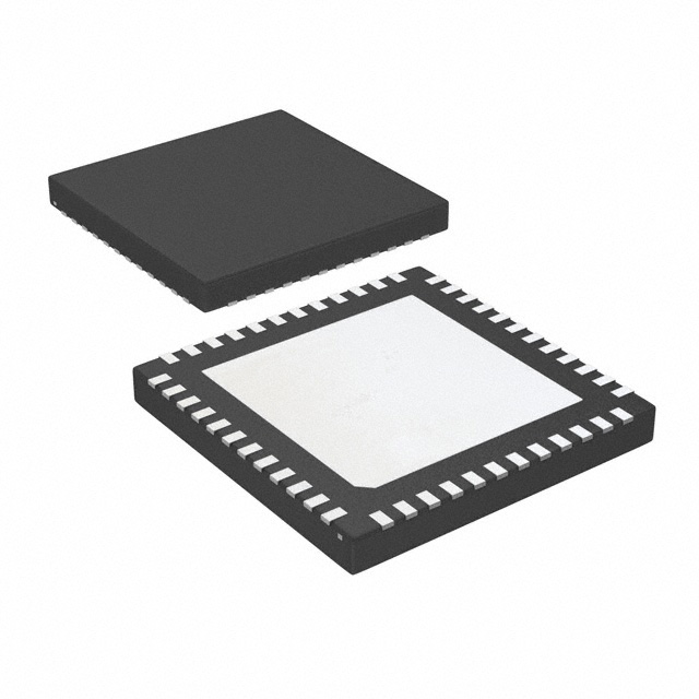
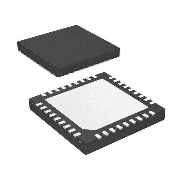
| 产品图片 |
|
| rohs | 符合RoHS无铅 / 符合限制有害物质指令(RoHS)规范要求 |
| 产品系列 | 接口 IC,LVDS 接口集成电路,Texas Instruments DS15MB200TSQ/NOPB- |
| 数据手册 | |
| 产品型号 | DS15MB200TSQ/NOPB |
| Tx/Rx类型 | LVDS |
| 产品目录页面 | |
| 产品种类 | LVDS 接口集成电路 |
| 传播延迟时间 | 2.5 ns |
| 供应商器件封装 | 48-WQFN(7X7) |
| 其它名称 | DS15MB200TSQ/NOPBDKR |
| 包装 | Digi-Reel® |
| 商标 | Texas Instruments |
| 安装类型 | 表面贴装 |
| 安装风格 | SMD/SMT |
| 封装 | Reel |
| 封装/外壳 | 48-WFQFN 裸露焊盘 |
| 封装/箱体 | LLP EP |
| 工作温度 | -40°C ~ 85°C |
| 工作电源电压 | 3.3 V |
| 工厂包装数量 | 250 |
| 应用 | LVDS |
| 延迟时间 | 1.0ns |
| 接收机数量 | 3 |
| 数据速率 | 1500 Mb/s |
| 数据速率(最大值) | 1.5Gbps |
| 最大工作温度 | + 85 C |
| 最小工作温度 | - 40 C |
| 标准包装 | 1 |
| 激励器数量 | 3 |
| 电压-电源 | 3 V ~ 3.6 V |
| 电容-输入 | 2pF |
| 电流-电源 | 225mA |
| 电源电压-最大 | 3.6 V |
| 电源电压-最小 | 3 V |
| 类型 | 缓冲器, 多路复用器 |
| 系列 | DS15MB200 |
| 输入 | BLVDS, CML, LVDS, LVPECL |
| 输出 | LVDS |
| 输出类型 | LVDS |
| 通道数 | 4 x 1:2, 2:1 |


- 商务部:美国ITC正式对集成电路等产品启动337调查
- 曝三星4nm工艺存在良率问题 高通将骁龙8 Gen1或转产台积电
- 太阳诱电将投资9.5亿元在常州建新厂生产MLCC 预计2023年完工
- 英特尔发布欧洲新工厂建设计划 深化IDM 2.0 战略
- 台积电先进制程称霸业界 有大客户加持明年业绩稳了
- 达到5530亿美元!SIA预计今年全球半导体销售额将创下新高
- 英特尔拟将自动驾驶子公司Mobileye上市 估值或超500亿美元
- 三星加码芯片和SET,合并消费电子和移动部门,撤换高东真等 CEO
- 三星电子宣布重大人事变动 还合并消费电子和移动部门
- 海关总署:前11个月进口集成电路产品价值2.52万亿元 增长14.8%


PDF Datasheet 数据手册内容提取
DS15MB200 www.ti.com SNLS196E–NOVEMBER2005–REVISEDMARCH2013 DS15MB200 Dual 1.5 Gbps 2:1/1:2 LVDS Mux/Buffer with Pre-Emphasis CheckforSamples:DS15MB200 FEATURES DESCRIPTION 1 • 1.5GbpsDataRatePerChannel The DS15MB200 is a dual-port 2 to 1 multiplexer and 2 1 to 2 repeater/buffer. High-speed data paths and • ConfigurableOff/OnPre-emphasisDrives flow-through pinout minimize internal device jitter and LossyBackplanesandCables simplify board layout, while pre-emphasis overcomes • LVDS/BLVDS/CML/LVPECLCompatibleInputs, ISI jitter effects from lossy backplanes and cables. LVDSCompatibleOutputs The differential inputs and outputs interface to LVDS or Bus LVDS signals such as those on Texas • LowOutputSkewandJitter Instrument's 10-, 16-, and 18-bit Bus LVDS SerDes, • On-chip100Ω InputandOutputTermination ortoCMLorLVPECLsignals. • 15kVESDProtectiononLVDSInputs/Outputs The 3.3V supply, CMOS process, and robust I/O • HotPlugProtection ensure high performance at low power over the entire • Single3.3VSupply industrial-40to+85°Ctemperaturerange. • Industrial-40to+85°CTemperatureRange • 48-pinWQFNPackage Typical Application Switch Fabric A ble a ane or C LVDS Mux Buffer LVDS FAPoSGrICA pl k Switch ac Fabric B B Figure1. 1 Pleasebeawarethatanimportantnoticeconcerningavailability,standardwarranty,anduseincriticalapplicationsof TexasInstrumentssemiconductorproductsanddisclaimerstheretoappearsattheendofthisdatasheet. Alltrademarksarethepropertyoftheirrespectiveowners. 2 PRODUCTIONDATAinformationiscurrentasofpublicationdate. Copyright©2005–2013,TexasInstrumentsIncorporated Products conform to specifications per the terms of the Texas Instruments standard warranty. Production processing does not necessarilyincludetestingofallparameters.
DS15MB200 SNLS196E–NOVEMBER2005–REVISEDMARCH2013 www.ti.com Block Diagram PREA_0 ENA_0 PREB_0 ENB_0 LI_0 SOA_0 SOB_0 PREL_0 ENL_0 SIA_0 LO_0 SIB_0 MUX_S0 Channel 0 Channel 1 Figure2. PINDESCRIPTIONS Pin WQFNPin I/O,Type Description Name Number SWITCHSIDEDIFFERENTIALINPUTS SIA_0+ 30 I,LVDS SwitchA-sideChannel0invertingandnon-invertingdifferentialinputs.LVDS,BusLVDS,CML,or SIA_0− 29 LVPECLcompatible. SIA_1+ 19 I,LVDS SwitchA-sideChannel1invertingandnon-invertingdifferentialinputs.LVDS,BusLVDS,CML,or SIA_1− 20 LVPECLcompatible. SIB_0+ 28 I,LVDS SwitchB-sideChannel0invertingandnon-invertingdifferentialinputs.LVDS,BusLVDS,CML,or SIB_0− 27 LVPECLcompatible. SIB_1+ 21 I,LVDS SwitchB-sideChannel1invertingandnon-invertingdifferentialinputs.LVDS,BusLVDS,CML,or SIB_1− 22 LVPECLcompatible. LINESIDEDIFFERENTIALINPUTS LI_0+ 40 I,LVDS Line-sideChannel0invertingandnon-invertingdifferentialinputs.LVDS,BusLVDS,CML,or LI_0− 39 LVPECLcompatible. LI_1+ 9 I,LVDS Line-sideChannel1invertingandnon-invertingdifferentialinputs.LVDS,BusLVDS,CML,or LI_1− 10 LVPECLcompatible. SWITCHSIDEDIFFERENTIALOUTPUTS SOA_0+ 34 O,LVDS SwitchA-sideChannel0invertingandnon-invertingdifferentialoutputs.LVDScompatible(1)(2). SOA_0− 33 SOA_1+ 15 O,LVDS SwitchA-sideChannel1invertingandnon-invertingdifferentialoutputs.LVDScompatible(1)(2). SOA_1− 16 SOB_0+ 32 O,LVDS SwitchB-sideChannel0invertingandnon-invertingdifferentialoutputs.LVDScompatible(1)(2). SOB_0− 31 SOB_1+ 17 O,LVDS SwitchB-sideChannel1invertingandnon-invertingdifferentialoutputs.LVDScompatible(1)(2). SOB_1− 18 LINESIDEDIFFERENTIALOUTPUTS LO_0+ 42 O,LVDS Line-sideChannel0invertingandnon-invertingdifferentialoutputs.LVDScompatible(1)(2). LO_0− 41 LO_1+ 7 O,LVDS Line-sideChannel1invertingandnon-invertingdifferentialoutputs.LVDScompatible(1)(2). LO_1− 8 (1) ForinterfacingLVDSoutputstoCMLorLVPECLcompatibleinputs,refertotheapplicationssectionofthisdatasheet(planned). (2) TheLVDSoutputsdonotsupportamultidrop(BLVDS)environment.TheLVDSoutputcharacteristicsoftheDS15MB200devicehave beenoptimizedforpoint-to-pointbackplaneandcableapplications. 2 SubmitDocumentationFeedback Copyright©2005–2013,TexasInstrumentsIncorporated ProductFolderLinks:DS15MB200
DS15MB200 www.ti.com SNLS196E–NOVEMBER2005–REVISEDMARCH2013 PINDESCRIPTIONS(continued) Pin WQFNPin I/O,Type Description Name Number DIGITALCONTROLINTERFACE MUX_S0 38 I,LVTTL MuxSelectControlInputs(perchannel)toselectwhichSwitch-sideinput,AorB,ispassedthrough MUX_S1 11 totheLine-side. PREA_0 26 I,LVTTL Outputpre-emphasiscontrolforSwitch-sideoutputs.EachoutputdriverontheSwitchA-sideandB- PREA_1 23 sidehasaseparatepintocontrolthepre-emphasisonoroff. PREB_0 25 PREB_1 24 PREL_0 44 I,LVTTL Outputpre-emphasiscontrolforLine-sideoutputs.EachoutputdriverontheLineA-sideandB-side PREL_1 5 hasaseparatepintocontrolthepre-emphasisonoroff. ENA_0 36 I,LVTTL OutputEnableControlforSwitchA-sideandB-sideoutputs.EachoutputdriverontheA-sideand ENA_1 13 B-sidehasaseparateenablepin. ENB_0 35 ENB_1 14 ENL_0 45 I,LVTTL OutputEnableControlforTheLine-sideoutputs.EachoutputdriverontheLine-sidehasaseparate ENL_1 4 enablepin. POWER V 2,6,12, I,Power V =3.3V±0.3V. DD DD 37,43,46, 48 GND 3,47(3) I,Power GroundreferenceforLVDSandCMOScircuitry. FortheWQFNpackage,theDAPisusedastheprimaryGNDconnectiontothedevice.TheDAPis theexposedmetalcontactatthebottomoftheWQFN-48package.Itshouldbeconnectedtothe groundplanewithatleast4viasforoptimalACandthermalperformance. (3) NotethattheDAPonthebacksideoftheWQFNpackageistheprimaryGNDconnectionforthedevicewhenusingtheWQFN package. Connection Diagrams VDD MUX_S1 LI_1- LI_1+ LO_1- LO-1+ VDD PREL_1 ENL_1 GND VDD N/C VDD MUX_S1 LI_1- LI_1+ LO_1- LO-1+ VDD PREL_1 ENL_1 GND VDD N/C 12 11 10 9 8 7 6 5 4 3 2 1 ENA_1 13 48 VDD ENA_1 VDD ENB_1 14 47 GND ENB_1 Channel 1 GND SOA_1+ 15 46 VDD SOA_1+ VDD SOA_1- 16 45 ENL_0 SOA_1- ENL_0 SOB_1+ 17 44 PREL_0 SOB_1+ PREL_0 Channel 0 SOB_1- 18 DAP 43 VDD SOB_1- VDD SIA_1+ 19 (GND) 42 LO_0+ SIA_1+ LO_0+ SIA_1- 20 41 LO_0- SIA_1- LO_0- SIB_1+ 21 40 LI_0+ SIB_1+ LI_0+ SIB_1- 22 39 LI_0- SIB_1- LI_0- PREA_1 23 38 MUX_S0 PREA_1 MUX_S0 PREB_1 24 37 VDD PREB_1 VDD 25 26 27 28 29 30 31 32 33 34 35 36 PREB_0 PREA_0 SIB_0- SIB_0+ SIA_0- SIA_0+ SOB_0- SOB_0+ SOA_0- SOA_0+ ENB_0 ENA_0 PREB_0 PREA_0 SIB_0- SIB_0+ SIA_0- SIA_0+ SOB_0- SOB_0+ SOA_0- SOA_0+ ENB_0 ENA_0 Figure3.WQFNTopView Figure4.DirectionalSignalPathsTopView DAP=GND (Refertopinnamesforsignalpolarity) Copyright©2005–2013,TexasInstrumentsIncorporated SubmitDocumentationFeedback 3 ProductFolderLinks:DS15MB200
DS15MB200 SNLS196E–NOVEMBER2005–REVISEDMARCH2013 www.ti.com Output Characteristics The output characteristics of the DS15MB200 have been optimized for point-to-point backplane and cable applications,andarenotintendedformultipointormultidropsignaling. A 100Ω output (source) termination resistor is incorporated in the device to eliminate the need for an external resistor, providing excellent drive characteristics by locating the source termination as close to the output as physicallypossible. Pre-Emphasis Controls The pre-emphasis is used to compensate for long or lossy transmission media. Separate pins are provided for each output to minimize power consumption. Pre-emphasis is programmable to be off or on per the Pre- emphasisControlTable. PREx_n(1) OutputPre-Emphasis 0 0% 1 100% (1) AppliestoPREA_0,PREA_1,PREB_0,PREB_1,PREL_0,PREL_1 Multiplexer Truth Table(2)(3) DataInputs ControlInputs Output SIA_0 SIB_0 MUX_S0 ENL_0 LO_0 X valid 0 1 SIB_0 valid X 1 1 SIA_0 X X X 0 Z (2) Samefunctionalityforchannel1 (3) X=Don'tCare Z=HighImpedance(TRI-STATE) Repeater/Buffer Truth Table(1)(2) DataInput ControlInputs Outputs LI_0 ENA_0 ENB_0 SOA_0 SOB_0 X 0 0 Z Z valid 0 1 Z LI_0 valid 1 0 LI_0 Z valid 1 1 LI_0 LI_0 (1) Samefunctionalityforchannel1 (2) X=Don'tCare Z=HighImpedance(TRI-STATE) Thesedeviceshavelimitedbuilt-inESDprotection.Theleadsshouldbeshortedtogetherorthedeviceplacedinconductivefoam duringstorageorhandlingtopreventelectrostaticdamagetotheMOSgates. 4 SubmitDocumentationFeedback Copyright©2005–2013,TexasInstrumentsIncorporated ProductFolderLinks:DS15MB200
DS15MB200 www.ti.com SNLS196E–NOVEMBER2005–REVISEDMARCH2013 Absolute Maximum Ratings(1) Value Unit SupplyVoltage(V ) −0.3to+4.0 V DD CMOSInputVoltage -0.3to (V +0.3) V DD LVDSReceiverInputVoltage(2) -0.3to (V +0.3) V DD LVDSDriverOutputVoltage -0.3to (V +0.3) V DD LVDSOutputShortCircuitCurrent +40 mA JunctionTemperature +150 °C StorageTemperature −65to+150 °C LeadTemperature(Solder,4sec) 260 °C MaxPkgPowerCapacity@25°C 5.2 W ThermalResistance(θ ) 24 °C/W JA PackageDeratingabove+25°C 41.7 mW/°C HBM,1.5kΩ,100pF 8 kV LVDSpinstoGNDonly 15 kV ESDLastPassingVoltage EIAJ,0Ω,200pF 250 V CDM 1000 V (1) Absolutemaximumratingsarethosevaluesbeyondwhichdamagetothedevicemayoccur.Thedatabookspecificationsshouldbemet, withoutexception,toensurethatthesystemdesignisreliableoveritspowersupply,temperature,andoutput/inputloadingvariables. TexasInstrumentsdoesnotrecommendoperationofproductsoutsideofrecommendedoperationconditions. (2) V max<2.4V ID Recommended Operating Conditions Min Max Unit SupplyVoltage(V ) 3.0 3.6 V CC InputVoltage(V)(1) 0 V V I CC OutputVoltage(V ) 0 V V O CC OperatingTemperature(T )Industrial −40 +85 °C A (1) V max<2.4V ID Copyright©2005–2013,TexasInstrumentsIncorporated SubmitDocumentationFeedback 5 ProductFolderLinks:DS15MB200
DS15MB200 SNLS196E–NOVEMBER2005–REVISEDMARCH2013 www.ti.com Electrical Characteristics Overrecommendedoperatingsupplyandtemperaturerangesunlessotherspecified. Symbol Parameter Conditions Min Typ(1) Max Units LVTTLDCSPECIFICATIONS(MUX_Sn,PREA_n,PREB_n,PREL_n,ENA_n,ENB_n,ENL_n) V HighLevelInputVoltage 2.0 V V IH DD V LowLevelInputVoltage GND 0.8 V IL I HighLevelInputCurrent V =V =V −10 +10 µA IH IN DD DDMAX I HighLevelInputCurrent PREA_n,PREB_n,PREL_n 40 200 µA IHR I LowLevelInputCurrent V =V ,V =V −10 +10 µA IL IN SS DD DDMAX C InputCapacitance AnyDigitalInputPintoV 2.0 pF IN1 SS C OutputCapacitance AnyDigitalOutputPintoV 4.0 pF OUT1 SS V InputClampVoltage I =−18mA −1.5 −0.8 V CL CL LVDSINPUTDCSPECIFICATIONS(SIA±,SIB±,LI±) V DifferentialInputHighThreshold(2) V =0.8Vor1.2Vor3.55V, TH CM 0 100 mV V =3.6V DD V DifferentialInputLowThreshold(2) V =0.8Vor1.2Vor3.55V, TL CM −100 0 mV V =3.6V DD V DifferentialInputVoltage V =0.8Vto3.55V,V =3.6V 100 2400 mV ID CM DD V CommonModeVoltageRange V =150mV,V =3.6V 0.05 3.55 V CMR ID DD C InputCapacitance IN+orIN−toV 2.0 pF IN2 SS I InputCurrent V =3.6V,V =V or0V −15 +15 µA IN IN DD DDMAX V =0V,V =V or0V −15 +15 µA IN DD DDMAX LVDSOUTPUTDCSPECIFICATIONS(SOA_n±,SOB_n±,LO_n±) V DifferentialOutputVoltage, R istheinternal100ΩbetweenOUT+ OD 0%Pre-emphasis(2) anLdOUT− 250 360 500 mV ΔV ChangeinV between OD OD -35 35 mV ComplementaryStates V OffsetVoltage(3) 1.05 1.22 1.475 V OS ΔV ChangeinV between OS OS -35 35 mV ComplementaryStates I OutputShortCircuitCurrent OUT+orOUT−ShorttoGND −21 -40 mA OS C OutputCapacitance OUT+orOUT−toGNDwhenTRI- OUT2 4.0 pF STATE SUPPLYCURRENT(Static) I SupplyCurrent Allinputsandoutputsenabledand CC active,terminatedwithexternalloadof 225 275 mA 100ΩbetweenOUT+andOUT-. I SupplyCurrent-PowerdownMode ENA_0=ENB_0=ENL_0=ENA_1= CCZ 0.6 4.0 mA ENB_1=ENL_1=L SWITCHINGCHARACTERISTICS—LVDSOUTPUTS t DifferentialLowtoHighTransition Useanalternating1and0patternat200 LHT 170 250 ps Time Mb/s,measurebetween20%and80%of V .(4) t DifferentialHightoLowTransition OD HLT 170 250 ps Time t DifferentialLowtoHighPropagation Useanalternating1and0patternat200 PLHD 1.0 2.5 ns Delay Mb/s,measureat50%V between OD inputtooutput. t DifferentialHightoLowPropagation PHLD 1.0 2.5 ns Delay t PulseSkew |t –t |(4) 25 75 ps SKD1 PLHD PHLD t OutputChanneltoChannelSkew Differenceinpropagationdelay(t or SKCC t )amongalloutputchannels.P(4L)HD 50 115 ps PHLD (1) TypicalparametersaremeasuredatV =3.3V,T =25°C.Theyareforreferencepurposes,andarenotproduction-tested. DD A (2) DifferentialoutputvoltageV isdefinedasABS(OUT+–OUT−).DifferentialinputvoltageV isdefinedasABS(IN+–IN−). OD ID (3) OutputoffsetvoltageV isdefinedastheaverageoftheLVDSsingle-endedoutputvoltagesatlogichighandlogiclowstates. OS (4) Notproductiontested.Guaranteedbystatisticalanalysisonasamplebasisatthetimeofcharacterization. 6 SubmitDocumentationFeedback Copyright©2005–2013,TexasInstrumentsIncorporated ProductFolderLinks:DS15MB200
DS15MB200 www.ti.com SNLS196E–NOVEMBER2005–REVISEDMARCH2013 Electrical Characteristics (continued) Overrecommendedoperatingsupplyandtemperaturerangesunlessotherspecified. Symbol Parameter Conditions Min Typ(1) Max Units t Jitter(0%Pre-emphasis)(5) RJ-Alternating1and0at750MHz(6) 1.1 1.5 psrms JIT DJ-K28.5Pattern,1.5Gbps(7) 20 34 psp-p TJ-PRBS27-1Pattern,1.5Gbps(8) 14 28 psp-p t LVDSOutputEnableTime TimefromENA_n,ENB_n,orENL_nto ON 0.5 1.5 µs OUT±changefromTRI-STATEtoactive. t LVDSOutputEnableTimefrom TimefromENA_n,ENB_n,orENL_nto ON2 PowerdownMode OUT±changefromPowerdownModeto 10 20 µs active. t LVDSOutputDisableTime TimefromENA_n,ENB_n,orENL_nto OFF OUT±changefromactivetoTRI-STATE 12 ns orPowerdownmode. (5) Jitterisnotproductiontested,butguaranteedthroughcharacterizationonasamplebasis. (6) RandomJitter,orRJ,ismeasuredRMSwithahistogramincluding1500histogramwindowhits.Theinputvoltage=V =500mV,50% ID dutycycleat750MHz,t =t =50ps(20%to80%). r f (7) DeterministicJitter,orD,ismeasuredtoahistogrammeanwithasamplesizeof350hits.Stimulusandfixturejitterhavebeen J subtracted.Theinputvoltage=V =500mV,K28.5patternat1.5Gbps,t =t =50ps(20%to80%).TheK28.5patternisrepeatingbit ID r f streamsof(00111110101100000101). (8) TotalJitter,orT,ismeasuredpeaktopeakwithahistogramincluding3500windowhits.Stimulusandfixturejitterhavebeen J subtracted.Theinputvoltage=V =500mV,27-1PRBSpatternat1.5Gbps,t =t =50ps(20%to80%). ID r f Copyright©2005–2013,TexasInstrumentsIncorporated SubmitDocumentationFeedback 7 ProductFolderLinks:DS15MB200
DS15MB200 SNLS196E–NOVEMBER2005–REVISEDMARCH2013 www.ti.com WQFN Performance Characteristics PowerSupplyCurrentvs.BitDataRate TotalJittervs.BitDataRate 350 60 mA) 300 50 ( PRE-EMPHASIS ON T PPLYCURREN 122505000 PRE-EMPHASIS OFF ALJITTER (ps) 3400 VCM = 1.2V U T 20 R S 100 TO VCM = 0.25V E W 10 O 50 P VCM = 3.0V 0 0 0 500 1000 1500 2000 0 500 1000 1500 2000 BITDATARATE (Mbps) BITDATARATE (Mbps) Dynamicpowersupplycurrentwasmeasuredwithallchannels TotalJittermeasuredat0VdifferentialwhilerunningaPRBS27-1 activeandtogglingatthebitdatarate.Datapatternhasnoeffect patternwithonechannelactive,allotherchannelsaredisabled. onthepowerconsumption. VDD=3.3V,TA=+25°C,VID=0.5V,pre-emphasisoff. V =3.3V,T =+25°C,V =0.5V,V =1.2V DD A ID CM Figure5. Figure6. TotalJittervs.Temperature 30 25 s) 20 p R ( E TT 15 JI L A T 10 O T 5 0 -40 -20 0 20 40 60 80 100 TEMPERATURE (°C) TotalJittermeasuredat0VdifferentialwhilerunningaPRBS27-1patternwithonechannelactive,allotherchannelsaredisabled.V = DD 3.3V,V =0.5V,V =1.2V,1.5Gbpsdatarate,pre-emphasisoff. ID CM Figure7. 8 SubmitDocumentationFeedback Copyright©2005–2013,TexasInstrumentsIncorporated ProductFolderLinks:DS15MB200
DS15MB200 www.ti.com SNLS196E–NOVEMBER2005–REVISEDMARCH2013 TRI-STATE AND POWERDOWN MODES The DS15MB200 has output enable control on each of the six onboard LVDS output drivers. This control allows each output individually to be placed in a low power TRI-STATE mode while the device remains active, and is useful to reduce power consumption on unused channels. In TRI-STATE mode, some outputs may remain active whilesomeareinTRI-STATE. When all six of the output enables (all drivers on both channels) are deasserted (LOW), then the device enters a Powerdown mode that consumes only 0.5mA (typical) of supply current. In this mode, the entire device is essentially powered off, including all receiver inputs, output drivers and internal bandgap reference generators. When returning to active mode from Powerdown mode, there is a delay until valid data is presented at the outputsbecauseoftheramptopoweruptheinternalbandgapreferencegenerators. Any single output enable that remains active will hold the device in active mode even if the other five outputs are inTRI-STATE. When in Powerdown mode, any output enable that becomes active will wake up the device back into active mode,eveniftheotherfiveoutputsareinTRI-STATE. Input Failsafe Biasing External pull up and pull down resistors may be used to provide enough of an offset to enable an input failsafe under open-circuit conditions. This configuration ties the positive LVDS input pin to VDD thru a pull up resistor and the negative LVDS input pin is tied to GND by a pull down resistor. The pull up and pull down resistors should be in the 5kΩ to 15kΩ range to minimize loading and waveform distortion to the driver. The common- mode bias point ideally should be set to approximately 1.2V (less than 1.75V) to be compatible with the internal circuitry. Please refer to application note AN-1194, “Failsafe Biasing of LVDS Interfaces” (SNLA051) for more information. Interfacing LVPECL to LVDS An LVPECL driver consists of a differential pair with coupled emitters connected to GND via a current source. This drives a pair of emitter-followers that require a 50 ohm to V -2.0 load. A modern LVPECL driver will CC typically include the termination scheme within the device for the emitter follower. If the driver does not include the load, then an external scheme must be used. The 1.3 V supply is usually not readily available on a PCB, therefore,aloadschemewithoutauniquepowersupplyrequirementmaybeused. 50: LVPECL 15MB200 50: R1 R2 150: 150: Figure8. DCCoupledLVPECLtoLVDSInterface Figure8isaseparatedπ terminationschemefora3.3VLVPECLdriver.R1andR2providesproperDCloadfor the driver emitter followers, and may be included as part of the driver device(1). The DS15MB200 includes a 100 ohm input termination for the transmission line. The common mode voltage will be at the normal LVPECL levels – around 2 V. This scheme works well with LVDS receivers that have rail-to-rail common mode voltage, V ,range.MostTexasInstrument'sLVDSreceivershavewideV range.Theexceptionsarenotedindevices’ CM CM respective datasheets. Those LVDS devices that do have a wide V range do not vary in performance CM significantlywhenreceivingasignalwithacommonmodeotherthanstandardLVDSV of1.2V. CM (1) ThebiasnetworksshownaboveforLVPECLdriversandreceiversmayormaynotbepresentwithinthedriverdevice.TheLVPECL driverandreceiverspecificationmustbereviewedcloselytoensurecompatibilitybetweenthedriverandreceiverterminationsand commonmodeoperatingranges. Copyright©2005–2013,TexasInstrumentsIncorporated SubmitDocumentationFeedback 9 ProductFolderLinks:DS15MB200
DS15MB200 SNLS196E–NOVEMBER2005–REVISEDMARCH2013 www.ti.com 0.1 PF 50: LVPECL 15MB200 50: 0.1 PF R1 R2 150: 150: Figure9. ACCoupledLVPECLtoLVDSInterface An AC coupled interface is preferred when transmitter and receiver ground references differ more than 1 V. This is a likely scenario when transmitter and receiver devices are on separate PCBs. Figure 9 illustrates an AC coupled interface between a LVPECL driver and LVDS receiver. R1 and R2, if not present in the driver device(2), provide DC load for the emitter followers and may range between 140-220 ohms for most LVPECL devices for this particular configuration. The DS15MB200 includes an internal 100 ohm resistor to terminate the transmission line for minimal reflections. The signal after AC coupling capacitors will swing around a level set by internal biasing resistors (i.e. fail-safe) which is either V /2 or 0 V depending on the actual failsafe implementation. If DD internalbiasingisnotimplemented,thesignalcommonmodevoltagewillslowlywandertoGNDlevel. Interfacing LVDS to LVPECL An LVDS driver consists of a current source (nominal 3.5mA) which drives a CMOS differential pair. It needs a differential resistive load in the range of 70 to 130 ohms to generate LVDS levels. In a system, the load should be selected to match transmission line characteristic differential impedance so that the line is properly terminated. The termination resistor should be placed as close to the receiver inputs as possible. When interfacing an LVDS driver with a non-LVDS receiver, one only needs to bias the LVDS signal so that it is within the common mode range of the receiver. This may be done by using separate biasing voltage which demands anotherpowersupply.Somereceivershaverequiredbiasingvoltageavailableon-chip(V ,V orV ). T TT BB 50: 15MB200 LVPECL 50: R1 R2 50: 50: VT Figure10. DCCoupledLVDStoLVPECLInterface Figure 10 illustrates interface between an LVDS driver and a LVPECL with a V pin available. R1 and R2, if not T present in the receiver(2), provide proper resistive load for the driver and termination for the transmission line, andV setsdesiredbiasforthereceiver. T (2) ThebiasnetworksshownaboveforLVPECLdriversandreceiversmayormaynotbepresentwithinthedriverdevice.TheLVPECL driverandreceiverspecificationmustbereviewedcloselytoensurecompatibilitybetweenthedriverandreceiverterminationsand commonmodeoperatingranges. 10 SubmitDocumentationFeedback Copyright©2005–2013,TexasInstrumentsIncorporated ProductFolderLinks:DS15MB200
DS15MB200 www.ti.com SNLS196E–NOVEMBER2005–REVISEDMARCH2013 VDD R1 R2 83: 83: 0.1 PF 50: 15MB200 LVPECL 50: 0.1 PF R3 R4 130: 130: Figure11. ACCoupledLVDStoLVPECLInterface Figure 11 illustrates AC coupled interface between an LVDS driver and LVPECL receiver without a V pin T available. The resistors R1, R2, R3, and R4, if not present in the receiver(2), provide a load for the driver, terminatethetransmissionline,andbiasthesignalforthereceiver. Packaging Information The Leadless Leadframe Package (WQFN) is a leadframe based chip scale package (CSP) that may enhance chip speed, reduce thermal impedance, and reduce the printed circuit board area required for mounting. The small size and very low profile make this package ideal for high density PCBs used in small-scale electronic applications such as cellular phones, pagers, and handheld PDAs. The WQFN package is offered in the no Pullback configuration. In the no Pullback configuration the standard solder pads extend and terminate at the edgeofthepackage.Thisfeatureoffersavisiblesolderfilletafterboardmounting. TheWQFNhasthefollowingadvantages: • Lowthermalresistance • Reducedelectricalparasitics • Improvedboardspaceefficiency • Reducedpackageheight • Reducedpackagemass For more details about WQFN packaging technology, refer to applications note AN-1187, "Leadless Leadframe Package"(SNOA401). Copyright©2005–2013,TexasInstrumentsIncorporated SubmitDocumentationFeedback 11 ProductFolderLinks:DS15MB200
DS15MB200 SNLS196E–NOVEMBER2005–REVISEDMARCH2013 www.ti.com REVISION HISTORY ChangesfromRevisionD(March2013)toRevisionE Page • ChangedlayoutofNationalDataSheettoTIformat.......................................................................................................... 11 12 SubmitDocumentationFeedback Copyright©2005–2013,TexasInstrumentsIncorporated ProductFolderLinks:DS15MB200
PACKAGE OPTION ADDENDUM www.ti.com 6-Feb-2020 PACKAGING INFORMATION Orderable Device Status Package Type Package Pins Package Eco Plan Lead/Ball Finish MSL Peak Temp Op Temp (°C) Device Marking Samples (1) Drawing Qty (2) (6) (3) (4/5) DS15MB200TSQ/NOPB ACTIVE WQFN RHS 48 250 Green (RoHS SN Level-3-260C-168 HR -40 to 85 15M200 & no Sb/Br) DS15MB200TSQX/NOPB ACTIVE WQFN RHS 48 2500 Green (RoHS SN Level-3-260C-168 HR -40 to 85 15M200 & no Sb/Br) (1) The marketing status values are defined as follows: ACTIVE: Product device recommended for new designs. LIFEBUY: TI has announced that the device will be discontinued, and a lifetime-buy period is in effect. NRND: Not recommended for new designs. Device is in production to support existing customers, but TI does not recommend using this part in a new design. PREVIEW: Device has been announced but is not in production. Samples may or may not be available. OBSOLETE: TI has discontinued the production of the device. (2) RoHS: TI defines "RoHS" to mean semiconductor products that are compliant with the current EU RoHS requirements for all 10 RoHS substances, including the requirement that RoHS substance do not exceed 0.1% by weight in homogeneous materials. Where designed to be soldered at high temperatures, "RoHS" products are suitable for use in specified lead-free processes. TI may reference these types of products as "Pb-Free". RoHS Exempt: TI defines "RoHS Exempt" to mean products that contain lead but are compliant with EU RoHS pursuant to a specific EU RoHS exemption. Green: TI defines "Green" to mean the content of Chlorine (Cl) and Bromine (Br) based flame retardants meet JS709B low halogen requirements of <=1000ppm threshold. Antimony trioxide based flame retardants must also meet the <=1000ppm threshold requirement. (3) MSL, Peak Temp. - The Moisture Sensitivity Level rating according to the JEDEC industry standard classifications, and peak solder temperature. (4) There may be additional marking, which relates to the logo, the lot trace code information, or the environmental category on the device. (5) Multiple Device Markings will be inside parentheses. Only one Device Marking contained in parentheses and separated by a "~" will appear on a device. If a line is indented then it is a continuation of the previous line and the two combined represent the entire Device Marking for that device. (6) Lead/Ball Finish - Orderable Devices may have multiple material finish options. Finish options are separated by a vertical ruled line. Lead/Ball Finish values may wrap to two lines if the finish value exceeds the maximum column width. Important Information and Disclaimer:The information provided on this page represents TI's knowledge and belief as of the date that it is provided. TI bases its knowledge and belief on information provided by third parties, and makes no representation or warranty as to the accuracy of such information. Efforts are underway to better integrate information from third parties. TI has taken and continues to take reasonable steps to provide representative and accurate information but may not have conducted destructive testing or chemical analysis on incoming materials and chemicals. TI and TI suppliers consider certain information to be proprietary, and thus CAS numbers and other limited information may not be available for release. In no event shall TI's liability arising out of such information exceed the total purchase price of the TI part(s) at issue in this document sold by TI to Customer on an annual basis. Addendum-Page 1
PACKAGE OPTION ADDENDUM www.ti.com 6-Feb-2020 Addendum-Page 2
PACKAGE MATERIALS INFORMATION www.ti.com 20-Sep-2016 TAPE AND REEL INFORMATION *Alldimensionsarenominal Device Package Package Pins SPQ Reel Reel A0 B0 K0 P1 W Pin1 Type Drawing Diameter Width (mm) (mm) (mm) (mm) (mm) Quadrant (mm) W1(mm) DS15MB200TSQ/NOPB WQFN RHS 48 250 178.0 16.4 7.3 7.3 1.3 12.0 16.0 Q1 DS15MB200TSQX/NOPB WQFN RHS 48 2500 330.0 16.4 7.3 7.3 1.3 12.0 16.0 Q1 PackMaterials-Page1
PACKAGE MATERIALS INFORMATION www.ti.com 20-Sep-2016 *Alldimensionsarenominal Device PackageType PackageDrawing Pins SPQ Length(mm) Width(mm) Height(mm) DS15MB200TSQ/NOPB WQFN RHS 48 250 210.0 185.0 35.0 DS15MB200TSQX/NOPB WQFN RHS 48 2500 367.0 367.0 38.0 PackMaterials-Page2
PACKAGE OUTLINE RHS0048A WQFN - 0.8 mm max height SCALE 1.800 PLASTIC QUAD FLATPACK - NO LEAD A 7.15 B 6.85 PIN 1 INDEX AREA 0.5 0.3 7.15 6.85 0.30 0.18 DETAIL OPTIONAL TERMINAL TYPICAL 0.8 0.7 C DIM A SEATING PLANE OPT 1 OPT 2 0.05 0.08 C (0.1) (0.2) 0.00 2X 5.5 (0.2) 5.1 0.1 (A) TYP 44X 0.5 13 24 12 25 EXPOSED THERMAL PAD 2X 49 SYMM 5.5 SEE TERMINAL DETAIL 1 36 0.30 48X 48 37 0.18 PIN 1 ID SYMM 0.5 0.1 C A B (OPTIONAL) 48X 0.3 0.05 4214990/B 04/2018 NOTES: 1. All linear dimensions are in millimeters. Any dimensions in parenthesis are for reference only. Dimensioning and tolerancing per ASME Y14.5M. 2. This drawing is subject to change without notice. 3. The package thermal pad must be soldered to the printed circuit board for thermal and mechanical performance. www.ti.com
EXAMPLE BOARD LAYOUT RHS0048A WQFN - 0.8 mm max height PLASTIC QUAD FLATPACK - NO LEAD ( 5.1) SYMM 48 37 48X (0.6) 1 36 48X (0.25) (1.05) TYP 44X (0.5) (1.25) TYP 49 SYMM (6.8) (R0.05) TYP ( 0.2) TYP VIA 12 25 13 24 (1.25) (1.05) TYP TYP (6.8) LAND PATTERN EXAMPLE EXPOSED METAL SHOWN SCALE:12X 0.07 MAX 0.07 MIN ALL AROUND ALL AROUND SOLDER MASK METAL EDGE OPENING EXPOSED METAL SOLDER MASK EXPOSED METAL UNDER OPENING METAL SOLDER MASK NON SOLDER MASK SOLDER MASK DEFINED DEFINED (PREFERRED) SOLDER MASK DETAILS 4214990/B 04/2018 NOTES: (continued) 4. This package is designed to be soldered to a thermal pad on the board. For more information, see Texas Instruments literature number SLUA271 (www.ti.com/lit/slua271). 5. Vias are optional depending on application, refer to device data sheet. If any vias are implemented, refer to their locations shown on this view. It is recommended that vias under paste be filled, plugged or tented. www.ti.com
EXAMPLE STENCIL DESIGN RHS0048A WQFN - 0.8 mm max height PLASTIC QUAD FLATPACK - NO LEAD (0.625) TYP (1.25) TYP 48 37 48X (0.6) 1 49 36 48X (0.25) 44X (0.5) (1.25) TYP (0.625) TYP SYMM (6.8) (R0.05) TYP METAL TYP 12 25 13 24 16X SYMM ( 1.05) (6.8) SOLDER PASTE EXAMPLE BASED ON 0.125 mm THICK STENCIL EXPOSED PAD 49 68% PRINTED SOLDER COVERAGE BY AREA UNDER PACKAGE SCALE:15X 4214990/B 04/2018 NOTES: (continued) 6. Laser cutting apertures with trapezoidal walls and rounded corners may offer better paste release. IPC-7525 may have alternate design recommendations. www.ti.com
IMPORTANTNOTICEANDDISCLAIMER TI PROVIDES TECHNICAL AND RELIABILITY DATA (INCLUDING DATASHEETS), DESIGN RESOURCES (INCLUDING REFERENCE DESIGNS), APPLICATION OR OTHER DESIGN ADVICE, WEB TOOLS, SAFETY INFORMATION, AND OTHER RESOURCES “AS IS” AND WITH ALL FAULTS, AND DISCLAIMS ALL WARRANTIES, EXPRESS AND IMPLIED, INCLUDING WITHOUT LIMITATION ANY IMPLIED WARRANTIES OF MERCHANTABILITY, FITNESS FOR A PARTICULAR PURPOSE OR NON-INFRINGEMENT OF THIRD PARTY INTELLECTUAL PROPERTY RIGHTS. These resources are intended for skilled developers designing with TI products. You are solely responsible for (1) selecting the appropriate TI products for your application, (2) designing, validating and testing your application, and (3) ensuring your application meets applicable standards, and any other safety, security, or other requirements. These resources are subject to change without notice. TI grants you permission to use these resources only for development of an application that uses the TI products described in the resource. Other reproduction and display of these resources is prohibited. No license is granted to any other TI intellectual property right or to any third party intellectual property right. TI disclaims responsibility for, and you will fully indemnify TI and its representatives against, any claims, damages, costs, losses, and liabilities arising out of your use of these resources. TI’s products are provided subject to TI’s Terms of Sale (www.ti.com/legal/termsofsale.html) or other applicable terms available either on ti.com or provided in conjunction with such TI products. TI’s provision of these resources does not expand or otherwise alter TI’s applicable warranties or warranty disclaimers for TI products. Mailing Address: Texas Instruments, Post Office Box 655303, Dallas, Texas 75265 Copyright © 2020, Texas Instruments Incorporated