ICGOO在线商城 > 集成电路(IC) > 时钟/计时 - 延迟线 > DS1110S-500+

 Datasheet下载
- 型号: DS1110S-500+
- 制造商: Maxim
- 库位|库存: xxxx|xxxx
- 要求:
| 数量阶梯 | 香港交货 | 国内含税 |
| +xxxx | $xxxx | ¥xxxx |
查看当月历史价格
查看今年历史价格
DS1110S-500+产品简介:
ICGOO电子元器件商城为您提供DS1110S-500+由Maxim设计生产,在icgoo商城现货销售,并且可以通过原厂、代理商等渠道进行代购。 DS1110S-500+价格参考¥46.04-¥46.04。MaximDS1110S-500+封装/规格:时钟/计时 - 延迟线, Delay Line IC 不可编程 10 Tap 500ns 16-SOIC(0.295",7.50mm 宽)。您可以下载DS1110S-500+参考资料、Datasheet数据手册功能说明书,资料中有DS1110S-500+ 详细功能的应用电路图电压和使用方法及教程。
Maxim Integrated的DS1110S-500+是一款基于硅技术的可编程延迟线芯片,广泛应用于需要精确时间延迟控制的电子系统中。其主要功能是提供精确且可编程的信号延迟,适用于通信、工业控制、测试测量设备以及精密时序控制等场景。

在通信系统中,DS1110S-500+可用于时钟信号的精确对齐和同步,确保数据传输的稳定性与可靠性。在工业自动化领域,该器件可帮助实现传感器信号的延迟匹配和设备之间的协调控制,提高系统整体精度。在测试与测量设备中,它可用于生成精确的触发信号或对信号进行时间校准,从而提升测试的准确性。

此外,DS1110S-500+也适用于需要时间延迟调节的音频或视频系统,如多声道音频同步、视频信号处理等应用。其低功耗、小封装设计使其特别适合空间受限且对功耗敏感的应用场景。

综上所述,DS1110S-500+凭借其高精度、可编程性和灵活性,广泛应用于通信、工业、测试设备及多媒体系统等各类需要精密时间控制的电子系统中。
| 参数 | 数值 |
| 产品目录 | 集成电路 (IC)半导体 |
| 描述 | IC DELAY LINE 10TAP 500NS 16SOIC延迟线/计时元素 5V 10-Tap Silicon De Delay Line |
| 产品分类 | |
| 品牌 | Maxim Integrated |
| 产品手册 | |
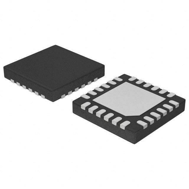
| 产品图片 |
|
| rohs | 符合RoHS无铅 / 符合限制有害物质指令(RoHS)规范要求 |
| 产品系列 | 时钟和计时器IC,延迟线/计时元素,Maxim Integrated DS1110S-500+- |
| 数据手册 | |
| 产品型号 | DS1110S-500+ |
| 产品培训模块 | http://www.digikey.cn/PTM/IndividualPTM.page?site=cn&lang=zhs&ptm=25703http://www.digikey.cn/PTM/IndividualPTM.page?site=cn&lang=zhs&ptm=25705 |
| 产品种类 | 延迟线/计时元素 |
| 供应商器件封装 | 16-SOIC W |
| 其它名称 | DS1110S500 |
| 功能 | Active Tapped Delay Line |
| 包装 | 管件 |
| 可用总延迟 | 500ns |
| 商标 | Maxim Integrated |
| 安装类型 | 表面贴装 |
| 安装风格 | SMD/SMT |
| 封装 | Tube |
| 封装/外壳 | 16-SOIC(0.295",7.50mm 宽) |
| 封装/箱体 | SOIC-Wide-16 |
| 工作温度 | -40°C ~ 85°C |
| 工厂包装数量 | 45 |
| 应用说明 | |
| 延迟到第一抽头 | 50ns |
| 抽头/步数 | 10 |
| 抽头增量 | 50ns |
| 最大工作温度 | + 85 C |
| 最小工作温度 | - 40 C |
| 标准包装 | 45 |
| 独立延迟数 | 1 |
| 电压-电源 | 4.75 V ~ 5.25 V |
| 电源电压-最大 | 5.25 V |
| 电源电压-最小 | 4.75 V |
| 系列 | DS1110S |
| 零件号别名 | 90-1110S+500 DS1110S |

.jpg)


- 商务部:美国ITC正式对集成电路等产品启动337调查
- 曝三星4nm工艺存在良率问题 高通将骁龙8 Gen1或转产台积电
- 太阳诱电将投资9.5亿元在常州建新厂生产MLCC 预计2023年完工
- 英特尔发布欧洲新工厂建设计划 深化IDM 2.0 战略
- 台积电先进制程称霸业界 有大客户加持明年业绩稳了
- 达到5530亿美元!SIA预计今年全球半导体销售额将创下新高
- 英特尔拟将自动驾驶子公司Mobileye上市 估值或超500亿美元
- 三星加码芯片和SET,合并消费电子和移动部门,撤换高东真等 CEO
- 三星电子宣布重大人事变动 还合并消费电子和移动部门
- 海关总署:前11个月进口集成电路产品价值2.52万亿元 增长14.8%


PDF Datasheet 数据手册内容提取
Rev 1; 11/03 10-Tap Silicon Delay Line General Description Features D The DS1110 delay line is an improved replacement for ♦ All-Silicon, 5V, 10-Tap Delay Line S the DS1010. It has ten equally spaced taps providing ♦ Improved, Drop-In Replacement for the DS1010 1 delays from 5ns to 500ns. The devices are offered in a 1 standard 16-pin SO or 14-pin TSSOP. The DS1110 series ♦ 10 Taps Equally Spaced 1 delay lines provide a nominal accuracy of ±5% or ±2ns, ♦ Delays are Stable and Precise whichever is greater, at 5V and +25°C. The DS1110 0 reproduces the input logic state at the tap 10 output after ♦ Leading- and Trailing-Edge Accuracy a fixed delay as specified by the dash number extension ♦ Delay Tolerance ±5% or ±2ns, whichever is of the part number. The DS1110 is designed to produce Greater, at 5V and +25°C both leading- and trailing-edge delays with equal preci- sion. Each tap is capable of driving up to ten 74LS type ♦ Economical loads. Dallas Semiconductor can customize standard ♦ Auto-Insertable, Low Profile products to meet special needs. ♦ Low-Power CMOS ♦ TTL/CMOS Compatible Applications ♦ Vapor Phase, IR, and Wave Solderable Communications Equipment ♦ Fast-Turn Prototypes Medical Devices ♦ Delays Specified Over Commercial and Industrial Automated Test Equipment Temperature Ranges PC Peripheral Devices ♦ Custom Delays Available ♦ Standard 16-Pin SO or 14-Pin TSSOP Pin Configurations Ordering Information PART TEMP RANGE PIN-PACKAGE DS1110E-XXX -40°C to +85°C 14 TSSOP TOP VIEW DS1110S-XXX -40°C to +85°C 16 SO IN 1 14 VCC N.C. 2 13 TAP1 TAP2 3 12 TAP3 DS1110E Selector Guide appears at end of data sheet. TAP4 4 11 TAP5 TAP6 5 10 TAP7 TAP8 6 9 TAP9 GND 7 8 TAP10 TSSOP Pin Configurations continued at end of data sheet. _____________________________________________Maxim Integrated Products 1 For pricing, delivery, and ordering information,please contact Maxim/Dallas Direct!at 1-888-629-4642, or visit Maxim’s website at www.maxim-ic.com.
10-Tap Silicon Delay Line 0 ABSOLUTE MAXIMUM RATINGS 1 Voltage on Any Pin Relative to Ground.................-0.5V to +6.0V Storage Temperature Range.............................-55°C to +125°C 1 Operating Temperature Range...........................-40°C to +85°C Soldering Temperature...................See IPC/JEDEC J-STD-020A 1 S D Stresses beyond those listed under “Absolute Maximum Ratings” may cause permanent damage to the device. These are stress ratings only, and functional operation of the device at these or any other conditions beyond those indicated in the operational sections of the specifications is not implied. Exposure to absolute maximum rating conditions for extended periods may affect device reliability. DC ELECTRICAL CHARACTERISTICS (VCC= 5.0V ±5%, TA= -40°C to +85°C.) PARAMETER SYMBOL CONDITIONS MIN TYP MAX UNITS Supply Voltage VCC (Note 1) 4.75 5.0 5.25 V VCC High-Level Input Voltage VIH (Note 1) 2.4 V + 0.3 Low-Level Input Voltage VIL (Note 1) -0.3 +0.8 V Input Leakage Current II 0V ≤ VI ≤ VCC -1.0 +1.0 µA Active Current ICC VCC = max, period = min (Note 2) 40 150 mA High-Level Output Current IOH VCC = min, VOH = 2.3V -1.0 mA Low-Level Output Current IOL VCC = min, VOL = 0.5V 12 mA AC ELECTRICAL CHARACTERISTICS (VCC= 5.0V ±5%, TA= -40°C to +85°C.) PARAMETER SYMBOL CONDITIONS MIN TYP MAX UNITS 10% of Input Pulse Width tWI (Note 6) ns tap 10 +25°C, 5.0V (Notes 3, 5, 6, 7, 9) -2 Table 1 +2 Input-to-Tap Delay tPLH (Delays ≤ 40ns) tPHL 0°C to +70°C (Notes 4–7) -3 Table 1 +3 ns -40°C to +85°C (Notes 4–7) -4 Table 1 +4 +25°C, 5.0V (Notes 3, 5, 6, 7, 9) -5 Table 1 +5 Input-to-Tap Delay tPLH 0°C to +70°C (Notes 4–7) -8 Table 1 +8 % (Delays > 40ns) tPHL -40°C to +85°C (Notes 4–7) -13 Table 1 +13 Power-Up Time tPU 200 ms 2 (tWI) or 20, Input Period Period (Note 8) whichever ns is greater 2 ______________________________________________________________________
10-Tap Silicon Delay Line CAPACITANCE D (TA= +25°C.) S PARAMETER SYMBOL CONDITIONS MIN TYP MAX UNITS 1 1 Input Capacitance CIN 5 10 pF 1 Note 1: All voltages are referenced to ground. 0 Note 2: Measured with outputs open. Note 3: Initial tolerances are ±with respect to the nominal value at +25°C and VCC= 5.0V for both leading and trailing edges. Note 4: Temperature and voltage tolerances are with respect to the actual delay measured over stated temperature range and a 4.75V to 5.25V range. Note 5: Intermediate delay values are available on a custom basis. Note 6: See Test Conditionssection. Note 7: All tap delays tend to vary unidirectionally with temperature or voltage changes. For example, if tap 1 slows down, all other taps also slow down; tap 3 can never be faster than tap 2. Note 8: Pulse width and period specifications may be exceeded; however, accuracy is application sensitive (decoupling, layout, etc.) Note 9: For Tap 1 delays greater than 20ns, the tolerance is ±3ns or ±5%, whichever is greater. Typical Operating Characteristics (VCC= 5.0V, TA= +25°C, unless otherwise noted.) DS1110-500 ACTIVE CURRENT DS1110-50 ACTIVE CURRENT vs. INPUT FREQUENCY vs. INPUT FREQUENCY 3450 DS1110 toc01 112680000 DS1110 toc02 mA) 30 mA) 140 NT ( 25 NT ( 120 RE RE UR 20 UR 100 C C ACTIVE 15 ACTIVE 6800 10 40 5 1V5CpCF = L 5O.2A5DV/TAP 20 1V5CpCF = L 5O.2A5DV/TAP 0 0 0.1 1.0 10 0.1 1.0 10 100 FREQUENCY (MHz) FREQUENCY (MHz) DS1110-500 TAP 10 DELAY DS1110-50 TAP 10 DELAY vs. TEMPERATURE vs. TEMPERATURE 555705 DS1110 toc03 5534 DS1110 toc04 52 525 DELAY (ns) 500 DELAY (ns) 5501 49 475 48 450 47 500kHz INPUT 425 46 -40 -15 10 35 60 85 -40 -15 10 35 60 85 TEMPERATURE (°C) TEMPERATURE (°C) _____________________________________________________________________ 3
10-Tap Silicon Delay Line 0 Typical Operating Characteristics (continued) 1 (VCC= 5.0V, TA= +25°C, unless otherwise noted.) 1 1 DS1110-500 DELAY vs. TAP DS1110-50 DELAY vs. TAP S D 445050000 FALLING EDGE DS1110 toc05 445050 FALLING EDGE DS1110 toc06 350 35 DELAY (ns) 223050000 RISING EDGE DELAY (ns) 223050 RISING EDGE 150 15 100 10 500kHz INPUT 50 5 0 0 1 2 3 4 5 6 7 8 9 10 1 2 3 4 5 6 7 8 9 10 TAP TAP DS1110-500 TAP 10 DELAY DS1110-50 TAP 10 DELAY vs. VOLTAGE vs. VOLTAGE 540 DS1110 toc07 5535 DS1110 toc08 520 DELAY (ns) 500 FALLING EDGE DELAY (ns) 4591 FALLING EDGE RISING EDGE RISING EDGE 480 47 500kHz INPUT 460 45 4.750 4.875 5.000 5.125 5.250 4.750 4.875 5.000 5.125 5.250 VOLTAGE (V) VOLTAGE (V) Pin Description PIN NAME FUNCTION TSSOP SO 1 1 IN Input 2 2, 3, 15 N.C. No Connection 7 8 GND Ground 13, 3, 12, 4, 11, 14, 4, 13, 5, 12, 6, 11, Tap 1–Tap 10 Tap Output Number 5, 10, 6, 9, 8 7, 10, 9 14 16 VCC 5.0V 4 ______________________________________________________________________
10-Tap Silicon Delay Line Detailed Description Table 1. Part Number by Delay (tPHL, tPLH) D The DS1110 delay line is an improved replacement for S the DS1010. It has ten equally spaced taps providing PART TOTAL DELAY* (ns) DELAY/TAP (ns) 1 delays from 5ns to 500ns. The devices are offered in a DS1110-50 50 5 1 standard 16-pin SO or 14-pin TSSOP. The DS1110 DS1110-60 60 6 1 series delay lines provide a nominal accuracy of ±5% DS1110-75 75 7.5 or ±2ns, whichever is greater, at 5V and +25°C. The 0 DS1110-80 80 8 DS1110 reproduces the input logic state at the tap 10 output after a fixed delay as specified by the dash DS1110-100 100 10 number extension of the part number. The DS1110 is DS1110-125 125 12.5 designed to produce both leading- and trailing-edge DS1110-150 150 15 delays with equal precision. Each tap is capable of dri- DS1110-175 175 17.5 ving up to ten 74LS type loads. Dallas Semiconductor can customize standard products to meet special DS1110-200 200 20 needs. For special requests call 972-371-4348. DS1110-250 250 25 DS1110-300 300 30 DS1110-350 350 35 DS1110-400 400 40 DS1110-450 450 45 DS1110-500 500 50 *Custom delays are available. TAP1 TAP2 TAP9 TAP10 IN 10% 10% 10% 10% Figure 1. Logic Diagram PERIOD tRISE tFALL VIH 2.2V 2.2V 1.5V 1.5V 1.5V 0.8V INVIL 0.8V tWI tWI tPLH tPLH 1.5V 1.5V OUT Figure 2. Timing Diagram: Silicon Delay Line _____________________________________________________________________ 5
10-Tap Silicon Delay Line 0 tPLH (Time Delay, Rising): The elapsed time between the 1.5V point on the leading edge of the input pulse 1 Terminology and the 1.5V point on the leading edge of any tap out- 1 Period: The time elapsed between the leading edge of put pulse. the first pulse and the leading edge of the following pulse. 1 S tWI (Pulse Width): The elapsed time on the pulse tPHL (Time Delay, Falling): The elapsed time between the 1.5V point on the trailing edge of the input pulse between the 1.5V point on the leading edge and the D and the 1.5V point on the trailing edge of any tap out- 1.5V point on the trailing edge, or the 1.5V point on the put pulse. trailing edge and the 1.5V point on the leading edge. tRISE(Input Rise Time):The elapsed time between the Test Setup Description 20% and the 80% point on the leading edge of the Figure 3 illustrates the hardware configuration used for input pulse. measuring the timing parameters on the DS1110. A precision pulse generator under software control pro- tFALL(Input Fall Time): The elapsed time between the duces the input waveform. Time delays are measured 80% and the 20% point on the trailing edge of the by a time interval counter (20ps resolution) connected input pulse. PULSE GENERATOR START Z0 = 50Ω TIME INTERVAL COUNTER STOP VHF SWITCH CONTROL UNIT DEVICE UNDER TEST Figure 3. Test Circuit 6 ______________________________________________________________________
10-Tap Silicon Delay Line between the input and each tap. Each tap is selected Table 2. Test Conditions D and connected to the counter by a VHF switch-control S unit. All measurements are fully automated, with each INPUT CONDITION instrument controlled by a central computer over an Ambient Temperature +25°C ±3°C 1 IEEE-488 bus. 1 Supply Voltage (VCC) 5.0V ±0.1V 1 Output High = 3.0V ±0.1V Input Pulse 0 Each output is loaded with the equivalent of one 74FO4 Low = 0.0V ±0.1V input gate. Delay is measured at the 1.5V level on the Source Impedance 50Ω max rising and falling edge. Rise and Fall Time 3ns max Pulse Width 500ns (1µs for -500ns) Period 1µs (2µs for -500ns) Chip Information Note:The above conditions are for test only and do not restrict the operation of the device under other data sheet conditions. TRANSISTOR COUNT: 6813 Selector Guide TOTAL TOTAL PIN- PIN- PART TEMP RANGE DELAY PART TEMP RANGE DELAY PACKAGE PACKAGE (ns)* (ns)* DS1110E-50 -40°C to +85°C 14 TSSOP 50 DS1110S-50 -40°C to +85°C 16 SO 50 DS1110E-60 -40°C to +85°C 14 TSSOP 60 DS1110S-60 -40°C to +85°C 16 SO 60 DS1110E-75 -40°C to +85°C 14 TSSOP 75 DS1110S-75 -40°C to +85°C 16 SO 75 DS1110E-80 -40°C to +85°C 14 TSSOP 80 DS1110S-80 -40°C to +85°C 16 SO 80 DS1110E-100 -40°C to +85°C 14 TSSOP 100 DS1110S-100 -40°C to +85°C 16 SO 100 DS1110E-125 -40°C to +85°C 14 TSSOP 125 DS1110S-125 -40°C to +85°C 16 SO 125 DS1110E-150 -40°C to +85°C 14 TSSOP 150 DS1110S-150 -40°C to +85°C 16 SO 150 DS1110E-175 -40°C to +85°C 14 TSSOP 175 DS1110S-175 -40°C to +85°C 16 SO 175 DS1110E-200 -40°C to +85°C 14 TSSOP 200 DS1110S-200 -40°C to +85°C 16 SO 200 DS1110E-250 -40°C to +85°C 14 TSSOP 250 DS1110S-250 -40°C to +85°C 16 SO 250 DS1110E-300 -40°C to +85°C 14 TSSOP 300 DS1110S-300 -40°C to +85°C 16 SO 300 DS1110E-350 -40°C to +85°C 14 TSSOP 350 DS1110S-350 -40°C to +85°C 16 SO 350 DS1110E-400 -40°C to +85°C 14 TSSOP 400 DS1110S-400 -40°C to +85°C 16 SO 400 DS1110E-450 -40°C to +85°C 14 TSSOP 450 DS1110S-450 -40°C to +85°C 16 SO 450 DS1110E-500 -40°C to +85°C 14 TSSOP 500 DS1110S-500 -40°C to +85°C 16 SO 500 *Custom delays are available. _____________________________________________________________________ 7
10-Tap Silicon Delay Line 0 Pin Configurations (continued) Package Information 1 For the latest package outline information, go to www.maxim-ic. 1 com/packages. TOP VIEW 1 S D IN1 1 16 VCC N.C. 2 15 N.C. N.C. 3 14 TAP1 TAP2 4 13 TAP3 DS1110S TAP4 5 12 TAP5 TAP6 6 11 TAP7 TAP8 7 10 TAP9 GND 8 9 TAP10 SO (300mil) Maxim cannot assume responsibility for use of any circuitry other than circuitry entirely embodied in a Maxim product. No circuit patent licenses are implied. Maxim reserves the right to change the circuitry and specifications without notice at any time. 8 _____________________Maxim Integrated Products, 120 San Gabriel Drive, Sunnyvale, CA 94086 408-737-7600 © 2002 Maxim Integrated Products Printed USA is a registered trademark of Maxim Integrated Products.
Mouser Electronics Authorized Distributor Click to View Pricing, Inventory, Delivery & Lifecycle Information: M axim Integrated: DS1110E-125 DS1110E-200 DS1110E-250 DS1110E-300 DS1110E-350 DS1110E-400 DS1110E-450 DS1110E- 50 DS1110E-500 DS1110E-60 DS1110E-80 DS1110S-100+ DS1110S-50+ DS1110E-100+ DS1110E-150+ DS1110E-175+ DS1110E-200+ DS1110E-250+ DS1110E-300+ DS1110E-350+ DS1110E-400+ DS1110E-450+ DS1110E-50+ DS1110E-500+ DS1110E-60+ DS1110E-75+ DS1110E-80+ DS1110S-100 DS1110S-125+ DS1110S-150 DS1110S-150+ DS1110S-200 DS1110S-200+ DS1110S-250 DS1110S-250+ DS1110S-300 DS1110S-300+ DS1110S-350+ DS1110S-400 DS1110S-400+ DS1110S-450+ DS1110S-50 DS1110S-500 DS1110S-500+ DS1110S-500+T DS1110S-60 DS1110S-60+ DS1110S-75 DS1110S-75+ DS1110S-80+