ICGOO在线商城 > 开发板,套件,编程器 > 评估和演示板和套件 > DRV8303EVM

 Datasheet下载
- 型号: DRV8303EVM
- 制造商: Texas Instruments
- 库位|库存: xxxx|xxxx
- 要求:
| 数量阶梯 | 香港交货 | 国内含税 |
| +xxxx | $xxxx | ¥xxxx |
查看当月历史价格
查看今年历史价格
DRV8303EVM产品简介:
ICGOO电子元器件商城为您提供DRV8303EVM由Texas Instruments设计生产,在icgoo商城现货销售,并且可以通过原厂、代理商等渠道进行代购。 DRV8303EVM价格参考¥783.68-¥783.68。Texas InstrumentsDRV8303EVM封装/规格:评估和演示板和套件, DRV8303, TMS320F28035 Motor Controller/Driver Power Management Evaluation Board。您可以下载DRV8303EVM参考资料、Datasheet数据手册功能说明书,资料中有DRV8303EVM 详细功能的应用电路图电压和使用方法及教程。
Texas Instruments(德州仪器)的DRV8303EVM是一款专门用于评估和测试DRV8303电机驱动器的开发板。它属于评估和演示板及套件类别,适用于多种电机驱动和控制应用场景。以下是DRV8303EVM的主要应用场景:

1. 无刷直流电机(BLDC)驱动:
   DRV8303EVM支持三相无刷直流电机的驱动和控制,能够提供高效率、低噪声的电机运行性能。适合家用电器、工业设备以及消费电子中的BLDC电机应用。

2. 电动工具开发:
   该评估板可以用于开发高性能电动工具,如电钻、电锯等。DRV8303的高集成度和高效能特性使其成为电动工具的理想选择。

3. 风机和泵控制:
   在需要精确速度控制的风机和泵系统中,DRV8303EVM可以帮助工程师快速评估和优化电机驱动性能,确保系统稳定运行。

4. 机器人技术:
   该评估板适用于小型和中型机器人的电机驱动设计,能够为机器人提供灵活的运动控制能力。

5. 电动车窗和座椅调节系统:
   在汽车领域,DRV8303EVM可用于评估电动车窗、座椅调节和其他辅助电机系统的驱动解决方案。

6. 教育和研发:
   对于高校和研究机构,DRV8303EVM是一个理想的工具,用于教学和研究电机驱动与控制技术。

DRV8303EVM集成了栅极驱动器、电流检测放大器和其他关键组件,简化了电机驱动系统的开发过程。通过使用该评估板,工程师可以快速验证设计概念,并加速产品上市时间。
| 参数 | 数值 |
| 产品目录 | 编程器,开发系统半导体 |
| 描述 | EVAL MODULE DRV8303电源管理IC开发工具 DRV8303 EVAL MOD |
| 产品分类 | |
| 品牌 | Texas Instruments |
| 产品手册 | |
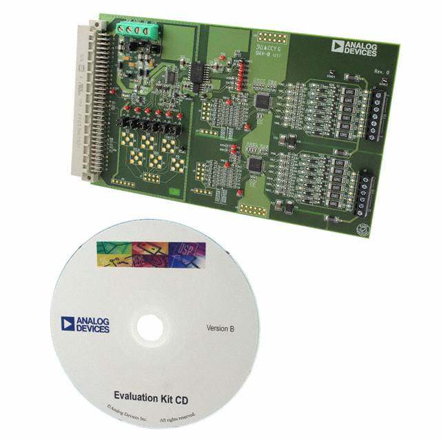
| 产品图片 |
|
| rohs | 符合RoHS无铅 / 符合限制有害物质指令(RoHS)规范要求 |
| 产品系列 | 电源管理IC开发工具,Texas Instruments DRV8303EVMC2000™, Piccolo™ |
| 数据手册 | 点击此处下载产品Datasheethttp://www.ti.com/lit/pdf/slvu983 |
| 产品型号 | DRV8303EVM |
| 主要属性 | 无刷交流(BLAC)或永磁同步电机(PMSM) |
| 主要用途 | 电源管理,电机控制 |
| 产品 | Evaluation Modules |
| 产品种类 | 电源管理IC开发工具 |
| 使用的IC/零件 | DRV8303, TMS320F28035 |
| 其它名称 | 296-37110 |
| 制造商产品页 | http://www.ti.com/general/docs/suppproductinfo.tsp?distId=10&orderablePartNumber=DRV8303EVM |
| 参考设计库 | http://www.digikey.com/rdl/4294959875/4294959892/1324 |
| 商标 | Texas Instruments |
| 嵌入式 | 是,MCU,32 位 |
| 工具用于评估 | DRV8303 |
| 所含物品 | 板,线缆 |
| 接口类型 | USB |
| 描述/功能 | Evaluation module for three phase pre-driver with dual current shunt amplifiers |
| 标准包装 | 1 |
| 特色产品 | http://www.digikey.cn/product-highlights/zh/texas-instruments-drv8303-threephase-predriver/51348 |
| 用于 | CCStudio v5.x, XDS100 JTAG Emulator |
| 类型 | Motor / Motion Controllers & Drivers |
| 系列 | DRV8303 |
| 辅助属性 | - |
| 输入电压 | 8 V to 60 V |


- 商务部:美国ITC正式对集成电路等产品启动337调查
- 曝三星4nm工艺存在良率问题 高通将骁龙8 Gen1或转产台积电
- 太阳诱电将投资9.5亿元在常州建新厂生产MLCC 预计2023年完工
- 英特尔发布欧洲新工厂建设计划 深化IDM 2.0 战略
- 台积电先进制程称霸业界 有大客户加持明年业绩稳了
- 达到5530亿美元!SIA预计今年全球半导体销售额将创下新高
- 英特尔拟将自动驾驶子公司Mobileye上市 估值或超500亿美元
- 三星加码芯片和SET,合并消费电子和移动部门,撤换高东真等 CEO
- 三星电子宣布重大人事变动 还合并消费电子和移动部门
- 海关总署:前11个月进口集成电路产品价值2.52万亿元 增长14.8%

PDF Datasheet 数据手册内容提取
Product Sample & Technical Tools & Support & Reference Folder Buy Documents Software Community Design DRV8303 SLOS846C–SEPTEMBER2013–REVISEDDECEMBER2016 DRV8303 Three-Phase Gate Driver With Dual-Current Shunt Amplifiers 1 Features 3 Description • 6-Vto60-VOperatingSupplyVoltageRange The DRV8303 is a gate driver IC for three-phase 1 motor-drive applications. The device provides three • 1.7-ASourceand2.3-ASinkGateDriveCurrent half bridge drivers, each capable of driving two N- Capability channel MOSFETs. The device supports up to 1.7-A • SlewRateControlforEMIReduction source and 2.3-A peak current capability. The • BootstrapGateDriverWith100%DutyCycle DRV8303 can operate off of a single power supply with a wide range from 6-V to 60-V. It uses a Support bootstrap gate-driver architecture with trickle charge • 6or3PWMInputModes circuitry to support 100% duty cycle. The DRV8303 • DualIntegratedCurrent-ShuntAmplifiersWith uses automatic hand shaking when the high-side or AdjustableGainandOffset low-side MOSFET is switching to prevent current shoot through. Integrated VDS sensing of the high- • 3.3-Vand5-VInterfaceSupport side and low-side MOSFETs is used to protect the • SerialPeripheralInterface(SPI) externalpowerstageagainstovercurrentconditions. • ProtectionFeatures: The DRV8303 includes two current-shunt amplifiers – ProgrammableDeadTimeControl(DTC) for accurate current measurement. The amplifiers – ProgrammableOvercurrentProtection(OCP) supportbi-directionalcurrentsensingandprovideand – PVDDandGVDDUndervoltageLockout adjustableoutputoffsetupto3V. (UVLO) The serial peripheral interface (SPI) provides detailed – GVDDOvervoltageLockout(OVLO) fault reporting and flexible parameter settings such as gainoptionsforthecurrent-shuntamplifiersandslew- – OvertemperatureWarning/Shutdown ratecontrolofthegatedrivers. (OTW/OTS) – ReportedthroughnFAULT,nOCTW,andSPI DeviceInformation(1) Registers PARTNUMBER PACKAGE BODYSIZE(NOM) DRV8303 TSSOP(48) 12.50mm×6.10mm 2 Applications (1) For all available packages, see the orderable addendum at • 3-PhaseBLDCandPMSMMotors theendofthedatasheet. • CPAPandPump • E-Bikes • PowerTools • RoboticsandRCToys • IndustrialAutomation SimplifiedSchematic 6 to 60 V PWM DRV8303 SPI Gate Drive 3-Phase el s Diff Amps Brushless nT U nE M C Pre-Driver aF M hS CO nFAULT Sense N-M Dual Shunt nOCTW Amps 1 An IMPORTANT NOTICE at the end of this data sheet addresses availability, warranty, changes, use in safety-critical applications, intellectualpropertymattersandotherimportantdisclaimers.PRODUCTIONDATA.
DRV8303 SLOS846C–SEPTEMBER2013–REVISEDDECEMBER2016 www.ti.com Table of Contents 1 Features.................................................................. 1 7.4 DeviceFunctionalModes........................................17 2 Applications........................................................... 1 7.5 Programming...........................................................19 3 Description............................................................. 1 7.6 RegisterMaps.........................................................20 4 RevisionHistory..................................................... 2 8 ApplicationandImplementation........................ 22 8.1 ApplicationInformation............................................22 5 PinConfigurationandFunctions......................... 3 8.2 TypicalApplication .................................................23 6 Specifications......................................................... 5 9 PowerSupplyRecommendations...................... 26 6.1 AbsoluteMaximumRatings......................................5 9.1 BulkCapacitance....................................................26 6.2 ESDRatings..............................................................5 10 Layout................................................................... 27 6.3 RecommendedOperatingConditions.......................6 6.4 ThermalInformation..................................................6 10.1 LayoutGuidelines.................................................27 6.5 ElectricalCharacteristics...........................................6 10.2 LayoutExample....................................................28 6.6 CurrentShuntAmplifierCharacteristics....................8 11 DeviceandDocumentationSupport................. 29 6.7 SPICharacteristics(SlaveModeOnly).....................8 11.1 DocumentationSupport........................................29 6.8 GateTimingandProtectionSwitching 11.2 ReceivingNotificationofDocumentationUpdates29 Characteristics...........................................................9 11.3 CommunityResources..........................................29 6.9 TypicalCharacteristics............................................10 11.4 Trademarks...........................................................29 7 DetailedDescription............................................ 11 11.5 ElectrostaticDischargeCaution............................29 7.1 Overview.................................................................11 11.6 Glossary................................................................29 7.2 FunctionalBlockDiagram.......................................12 12 Mechanical,Packaging,andOrderable 7.3 FeatureDescription.................................................13 Information........................................................... 29 4 Revision History NOTE:Pagenumbersforpreviousrevisionsmaydifferfrompagenumbersinthecurrentversion. ChangesfromRevisionB(November2015)toRevisionC Page • AddedthemaximumvoltagedifferenceandmaximumvoltageparametersfortheBST_X,GH_X,SL_X,andSH_X pinsintheAbsoluteMaximumRatingstable......................................................................................................................... 5 • AddedtheDocumentationsupportandReceivingNotificationofDocumentationUpdatessections ................................. 29 ChangesfromRevisionA(October2013)toRevisionB Page • AddedESDRatingstable,FeatureDescriptionsection,DeviceFunctionalModes,ApplicationandImplementation section,PowerSupplyRecommendationssection,Layoutsection,DeviceandDocumentationSupportsection,and Mechanical,Packaging,andOrderableInformationsection ................................................................................................. 1 • Updatedtitle............................................................................................................................................................................ 1 • V absolutemaxvoltageratingreducedfrom70Vto65V ............................................................................................. 5 PVDD • ClarificationmadeonhowtheOCPstatusbitsreportinOvercurrentProtection(OCP)andReporting ............................15 • UpdatetoPVDDundervoltageprotectioninUndervoltageProtection(UVLO)describingspecifictransientbrownout issue..................................................................................................................................................................................... 16 • UpdatetoEN_GATEpinfunctionaldescriptioninEN_GATEclarifyingproperEN_GATEresetpulselengths.................17 • Addedgatedriverpower-upsequencingerrata .................................................................................................................. 22 2 SubmitDocumentationFeedback Copyright©2013–2016,TexasInstrumentsIncorporated ProductFolderLinks:DRV8303
DRV8303 www.ti.com SLOS846C–SEPTEMBER2013–REVISEDDECEMBER2016 5 Pin Configuration and Functions DCAPackage 48-PinTSSOPPadDown TopView nOCTW 1 48 GND nFAULT 2 47 GND DTC 3 46 GND nSCS 4 45 VDD_SPI SDI 5 44 BST_A SDO 6 43 GH_A SCLK 7 42 SH_A DC_CAL 8 41 GL_A GVDD 9 D 40 SL_A A CP1 10 P 39 BST_B _ CP2 11 R 38 GH_B W EN_GATE 12 P 37 SH_B INH_A 13 9) - 36 GL_B INL_A 14 4 35 SL_B INH_B 15 D ( 34 BST_C N INL_B 16 G 33 GH_C INH_C 17 32 SH_C INL_C 18 31 GL_C DVDD 19 30 SL_C REF 20 29 SN1 SO1 21 28 SP1 SO2 22 27 SN2 AVDD 23 26 SP2 AGND 24 25 PVDD PinFunctions PIN I/O DESCRIPTION NO. NAME Overcurrentandovertemperaturewarningindicator.Thisoutputisopendrainwithexternalpullup 1 nOCTW O resistorrequired.ProgrammableoutputmodethroughSPIregisters. 2 nFAULT O Faultreportindicator.Thisoutputisopendrainwithexternalpullupresistorrequired. 3 DTC I Dead-timeadjustmentwithexternalresistortoGND 4 nSCS I SPIchipselect 5 SDI I SPIinput 6 SDO O SPIoutput 7 SCLK I SPIclocksignal WhenDC_CALishigh,deviceshortsinputsofshuntamplifiersanddisconnectsloads.DCoffset 8 DC_CAL I calibrationcanbedonethroughexternalmicrocontroller. 9 GVDD P Internalgatedrivervoltageregulator.GVDDcapshouldconnecttoGND 10 CP1 P Chargepumppin1,ceramiccapshouldbeusedbetweenCP1andCP2 11 CP2 P Chargepumppin2,ceramiccapshouldbeusedbetweenCP1andCP2 12 EN_GATE I Enablegatedriverandcurrentshuntamplifiers. 13 INH_A I PWMInputsignal(highside),half-bridgeA 14 INL_A I PWMInputsignal(lowside),half-bridgeA 15 INH_B I PWMInputsignal(highside),half-bridgeB 16 INL_B I PWMInputsignal(lowside),half-bridgeB 17 INH_C I PWMInputsignal(highside),half-bridgeC 18 INL_C I PWMInputsignal(lowside),half-bridgeC Copyright©2013–2016,TexasInstrumentsIncorporated SubmitDocumentationFeedback 3 ProductFolderLinks:DRV8303
DRV8303 SLOS846C–SEPTEMBER2013–REVISEDDECEMBER2016 www.ti.com PinFunctions(continued) PIN I/O DESCRIPTION NO. NAME Internal3.3-Vsupplyvoltage.DVDDcapshouldconnecttoAGND.Thisisanoutput,butnotspecifiedto 19 DVDD P driveexternalcircuitry. Referencevoltagetosetoutputofshuntamplifierswithabiasvoltagewhichequalstohalfofthe 20 REF I voltagesetonthispin.ConnecttoADCreferenceinmicrocontroller. 21 SO1 O Outputofcurrentamplifier1 22 SO2 O Outputofcurrentamplifier2 Internal6-Vsupplyvoltage,AVDDcapacitorshouldalwaysbeinstalledandconnectedtoAGND.Thisis 23 AVDD P anoutput,butnotspecifiedtodriveexternalcircuitry. 24 AGND P Analoggroundpin Powersupplypinforgatedriver,currentshuntamplifier,andSPIcommunication.PVDDcapshould 25 PVDD P connecttoGND Inputofcurrentamplifier2(connectingtopositiveinputofamplifier).Recommendtoconnecttoground 26 SP2 I sideofthesenseresistorforthebestcommonmoderejection. 27 SN2 I Inputofcurrentamplifier2(connectingtonegativeinputofamplifier). Inputofcurrentamplifier1(connectingtopositiveinputofamplifier).Recommendtoconnecttoground 28 SP1 I sideofthesenseresistorforthebestcommonmoderejection. 29 SN1 I Inputofcurrentamplifier1(connectingtonegativeinputofamplifier). Low-SideMOSFETsourceconnection,half-bridgeC.Low-sideV measuredbetweenthispinand 30 SL_C I DS SH_C. 31 GL_C O GatedriveoutputforLow-SideMOSFET,half-bridgeC High-SideMOSFETsourceconnection,half-bridgeC.High-sideV measuredbetweenthispinand 32 SH_C I DS PVDD. 33 GH_C O GatedriveoutputforHigh-SideMOSFET,half-bridgeC 34 BST_C P Bootstrapcapacitorpinforhalf-bridgeC Low-SideMOSFETsourceconnection,half-bridgeB.Low-sideV measuredbetweenthispinand 35 SL_B I DS SH_B. 36 GL_B O GatedriveoutputforLow-SideMOSFET,half-bridgeB High-SideMOSFETsourceconnection,half-bridgeB.High-sideV measuredbetweenthispinand 37 SH_B I DS PVDD. 38 GH_B O GatedriveoutputforHigh-SideMOSFET,half-bridgeB 39 BST_B P Bootstrapcappinforhalf-bridgeB Low-SideMOSFETsourceconnection,half-bridgeA.Low-sideV measuredbetweenthispinand 40 SL_A I DS SH_A. 41 GL_A O GatedriveoutputforLow-SideMOSFET,half-bridgeA High-SideMOSFETsourceconnection,half-bridgeA.High-sideV measuredbetweenthispinand 42 SH_A I DS PVDD. 43 GH_A O GatedriveoutputforHigh-SideMOSFET,half-bridgeA 44 BST_A P Bootstrapcapacitorpinforhalf-bridgeA 45 VDD_SPI I SPIsupplypintosupport3.3Vor5Vlogic.Connecttoeither3.3Vor5V. 469 47 GND GNDpin.Theexposedpowerpadmustbeelectricallyconnectedtogroundplanethroughsolderingto 48 O PCBforproperoperationandconnectedtobottomsideofPCBthroughviasforbetterthermal spreading. GND 49 (PWR_PAD) 4 SubmitDocumentationFeedback Copyright©2013–2016,TexasInstrumentsIncorporated ProductFolderLinks:DRV8303
DRV8303 www.ti.com SLOS846C–SEPTEMBER2013–REVISEDDECEMBER2016 6 Specifications 6.1 Absolute Maximum Ratings overoperatingfree-airtemperaturerange(unlessotherwisenoted)(1) MIN MAX UNIT Supplyvoltage RelativetoPGND –0.3 65 V V PVDD Maximumsupply-voltageramprate VoltagerisinguptoPVDD 1 V/µs MAX V MaximumvoltagebetweenPGNDandGND –0.3 0.3 V PGND V VoltageforSPxandSNxpins –0.6 0.6 V OPA_IN Inputvoltageforlogicanddigitalpins(INH_A,INL_A,INH_B,INL_B,INH_C,INL_C, V –0.3 7 V LOGIC EN_GATE,SCLK,SDI,SCS,DC_CAL) V MaximumvoltageforGVDDpin 13.2 V GVDD V MaximumvoltageforAVDDpin 8 V AVDD V MaximumvoltageforDVDDpin 3.6 V DVDD V MaximumvoltageforVDD_SPIpin 7 V VDD_SPI V V MaximumvoltageforSDOpin DD_SPI V SDO +0.3 V Maximumreferencevoltageforcurrentamplifier 7 V REF V MaximumvoltageforBST_XPin –0.3 80 V BST_MAX V Maximumvoltagedifferencefor(BST_X-SH_X)and(BST_X-GH_X) –0.3 14.5 V BST_DIFF V MaximumvoltageforGH_Xpin –0.3 80 V GH_MAX V Maximumvoltagedifferencefor(GH_X-SH_X) –0.3 14.5 V GH_DIF V MaximumvoltageforGL_Xpin –0.3 13.2 V GL_MAX V Maximumvoltagedifferencefor(GL_X-SL_X) –0.3 13.2 V GL_DIF V MaximumvoltageforSH_Xpin –2 PVDD+2 V SH_MAX V MaximumvoltageforSL_Xpin –0.6 0.6 V SL_MAX Maximumcurrentforalldigitalandanaloginputs(INH_A,INL_A,INH_B,INL_B, I –1 1 mA IN_MAX INH_C,INL_C,SCLK,SCS,SDI,EN_GATE,DC_CAL,DTC) I Maximumsinkingcurrentforopen-drainpins(nFAULTandnOCTWpins) 7 mA SINK_MAX I MaximumcurrentforREFpin 100 µA REF T Storagetemperature –55 150 °C stg (1) StressesbeyondthoselistedunderAbsoluteMaximumRatingsmaycausepermanentdamagetothedevice.Thesearestressratings only,whichdonotimplyfunctionaloperationofthedeviceattheseoranyotherconditionsbeyondthoseindicatedunderRecommended OperatingConditions.Exposuretoabsolute-maximum-ratedconditionsforextendedperiodsmayaffectdevicereliability. 6.2 ESD Ratings VALUE UNIT Humanbodymodel(HBM),perANSI/ESDA/JEDECJS-001(1) ±2000 V Electrostaticdischarge V (ESD) Chargeddevicemodel(CDM),perJEDECspecificationJESD22-C101(2) ±500 (1) JEDECdocumentJEP155statesthat500-VHBMallowssafemanufacturingwithastandardESDcontrolprocess. (2) JEDECdocumentJEP157statesthat250-VCDMallowssafemanufacturingwithastandardESDcontrolprocess. Copyright©2013–2016,TexasInstrumentsIncorporated SubmitDocumentationFeedback 5 ProductFolderLinks:DRV8303
DRV8303 SLOS846C–SEPTEMBER2013–REVISEDDECEMBER2016 www.ti.com 6.3 Recommended Operating Conditions Overoperatingfree-airtemperaturerange(unlessotherwisenoted). MIN NOM MAX UNIT V DCsupplyvoltagePVDDfornormaloperation RelativetoPGND 6 60 V PVDD I InputcurrentofdigitalpinswhenEN_GATEishigh 100 µA DIN_EN I InputcurrentofdigitalpinswhenEN_GATEislow 1 µA DIN_DIS C Maximumoutputcapacitanceonoutputsofshuntamplifier 20 pF O_OPA Deadtimecontrolresistor.Timerangeis50ns(–GND)to500ns(150kΩ)withalinear R 0 150 kΩ DTC approximation. I nFAULTpinsinkcurrent.Opendrain V=0.4V 2 mA FAULT I nOCTWpinsinkcurrent.Opendrain V=0.4V 2 mA OCTW V Externalvoltagereferencevoltageforcurrentshuntamplifiers 2 6 V REF Q =25nCortotal30-mAgate f Operatingswitchingfrequencyofgatedriver g(TOT) 200 kHz gate driveaveragecurrent I Totalaveragegatedrivecurrent 30 mA gate T Ambienttemperature –40 125 °C A 6.4 Thermal Information DRV8303 THERMALMETRIC(1) DCA(TSSOP) UNIT 48PINS R Junction-to-ambientthermalresistance 30.3 °C/W θJA R Junction-to-case(top)thermalresistance 33.5 °C/W θJC(top) R Junction-to-boardthermalresistance 17.5 °C/W θJB ψ Junction-to-topcharacterizationparameter 0.9 °C/W JT ψ Junction-to-boardcharacterizationparameter 7.2 °C/W JB R Junction-to-case(bottom)thermalresistance 0.9 °C/W θJC(bot) (1) Formoreinformationabouttraditionalandnewthermalmetrics,seetheSemiconductorandICPackageThermalMetricsapplication report. 6.5 Electrical Characteristics PVDD=6Vto60V,T =25°C,unlessspecifiedundertestcondition C PARAMETER TESTCONDITIONS MIN TYP MAX UNIT INPUTPINS:INH_X,INL_X,SCS,SDI,SCLK,EN_GATE,DC_CAL V Highinputthreshold 2 V IH V Lowinputthreshold 0.8 V IL RPULL_DOWN–INTERNALPULLDOWNRESISTORFORGATEDRIVERINPUTS R InternalpulldownresistorforEN_GATE 100 kΩ EN_GATE Internalpulldownresistorforhighside R EN_GATEhigh 100 kΩ INH_X PWMs(INH_A,INH_B,andINH_C) InternalpulldownresistorforlowsidePWMs R EN_GATEhigh 100 kΩ INH_X (INL_A,INL_B,andINL_C) R InternalpulldownresistorfornSCS EN_GATEhigh 100 kΩ SCS R InternalpulldownresistorforSDI EN_GATEhigh 100 kΩ SDI R InternalpulldownresistorforDC_CAL EN_GATEhigh 100 kΩ DC_CAL R InternalpulldownresistorforSCLK EN_GATEhigh 100 kΩ SCLK OUTPUTPINS:nFAULTANDnOCTW V Low-outputthreshold I =2mA 0.4 V OL O External47-kΩpullupresistorconnected V High-outputthreshold 2.4 V OH to3-5.5V 6 SubmitDocumentationFeedback Copyright©2013–2016,TexasInstrumentsIncorporated ProductFolderLinks:DRV8303
DRV8303 www.ti.com SLOS846C–SEPTEMBER2013–REVISEDDECEMBER2016 Electrical Characteristics (continued) PVDD=6Vto60V,T =25°C,unlessspecifiedundertestcondition C PARAMETER TESTCONDITIONS MIN TYP MAX UNIT Leakagecurrentonopendrainpinswhen I 1 µA OH logichigh(nFAULTandnOCTW) GATEDRIVEOUTPUT:GH_A,GH_B,GH_C,GL_A,GL_B,GL_C PVDD=8Vto60V,I =30mA, gate 9.5 11.5 C =22nF CP V GatedriverVgsvoltage V GX_NORM PVDD=8Vto60V,I =30mA, gate 9.5 11.5 C =220nF CP PVDD=6Vto8V,I =15mA, gate 8.8 C =22nF CP V GatedriverVgsvoltage V GX_MIN PVDD=6Vto8V,I =30mA, gate 8.3 C =220nF CP I Maximumsourcecurrentsetting1,peak VgsofFETequalsto2V.REG0x02 1.7 A oso1 I Maximumsinkcurrentsetting1,peak VgsofFETequalsto8V.REG0x02 2.3 A osi1 I Sourcecurrentsetting2,peak VgsofFETequalsto2V.REG0x02 0.7 A oso2 I Sinkcurrentsetting2,peak VgsofFETequalsto8V.REG0x02 1 A osi2 I Sourcecurrentsetting3,peak VgsofFETequalsto2V.REG0x02 0.25 A oso3 I Sinkcurrentsetting3,peak VgsofFETequalsto8V.REG0x02 0.5 A osi3 Gateoutputimpedanceduringstandby R modewhenEN_GATElow(pinsGH_x, 1.6 2.4 kΩ gate_off GL_x) SUPPLYCURRENTS I PVDDsupplycurrent,standby EN_GATEislow.PVDD=8V 20 50 µA PVDD_STB EN_GATEishigh,noloadongatedrive I PVDDsupplycurrent,operating output,switchingat10kHz, 15 mA PVDD_OP 100-nCgatecharge I PVDDsupplycurrent,Hi-Z EN_GATEishigh,gatenotswitching 2 5 10 mA PVDD_HIZ INTERNALREGULATORVOLTAGE PVDD=8Vto60V 6 6.5 7 A AVDDvoltage V VDD PVDD=6Vto8V 5.5 6 D DVDDvoltage 3 3.3 3.6 V VDD VOLTAGEPROTECTION V Undervoltageprotectionlimit,PVDD 6 V PVDD_UV V Undervoltageprotectionlimit,GVDD 7.5 V GVDD_UV V Overvoltageprotectionlimit,GVDD 16 V GVDD_OV CURRENTPROTECTION,(VDSSENSING) PVDD=8Vto60V 0.125 2.4 V Drain-sourcevoltageprotectionlimit V DS_OC PVDD=6Vto8V(1) 0.125 1.491 T OCsensingresponsetime 1.5 µs OC nOCTWpinreportingpulsestretchlengthfor T 64 µs OC_PULSE OCevent TEMPERATUREPROTECTION Junctiontemperatureforresettingover OTW_CLR 115 °C temperaturewarning Junctiontemperatureforovertemperature OTW_SET/ warningandresettingovertemperatureshut 130 °C OTSD_CLR down Junctiontemperatureforovertemperature OTSD_SET 150 °C shutdown (1) ReducedA voltagerangeresultsinlimitationsonsettingsforovercurrentprotection.SeeTable12. VDD Copyright©2013–2016,TexasInstrumentsIncorporated SubmitDocumentationFeedback 7 ProductFolderLinks:DRV8303
DRV8303 SLOS846C–SEPTEMBER2013–REVISEDDECEMBER2016 www.ti.com 6.6 Current Shunt Amplifier Characteristics Overoperatingfree-airtemperaturerange. PARAMETER TESTCONDITIONS MIN TYP MAX UNIT G1 Gainoption1 Tc=–40°Cto125°C 9.5 10 10.5 V/V G2 Gainoption2 Tc=–40°Cto125°C 18 20 21 V/V G3 GainOption3 Tc=–40°Cto125°C 38 40 42 V/V G4 GainOption4 Tc=–40°Cto125°C 75 80 85 V/V Tsettling Settlingtimeto1% Tc=0to60°C,G=10,Vstep=2V 300 ns Tsettling Settlingtimeto1% Tc=0to60°C,G=20,Vstep=2V 600 ns Tsettling Settlingtimeto1% Tc=0to60°C,G=40,Vstep=2V 1.2 µs Tsettling Settlingtimeto1% Tc=0to60°C,G=80,Vstep=2V 2.4 µs Vswing Outputswinglinearrange 0.3 5.7 V SlewRate G=10 10 V/µs DC_offset OffseterrorRTI G=10withinputshorted 4 mV Drift_offset OffsetdriftRTI 10 µV/C Ibias Inputbiascurrent 100 µA Vin_com Commoninputmoderange –0.15 0.15 V Vin_dif Differentialinputrange –0.3 0.3 V Withzeroinputcurrent,V upto Vo_bias Outputbias REF –0.5% 0.5×Vref 0.5% V 6V OverallCMRRwithgainresistor CMRR_OV CMRRatDC,gain=10 70 85 dB mismatch 6.7 SPI Characteristics (Slave Mode Only) MIN NOM MAX UNIT SPIreadyafterEN_GATEtransitions t PVDD>6V 5 10 ms SPI_READY toHIGH t MinimumSPIclockperiod 100 ns CLK t Clockhightime SeeFigure1 40 ns CLKH t Clocklowtime SeeFigure1 40 ns CLKL t SDIinputdatasetuptime 20 ns SU_SDI t SDIinputdataholdtime 30 ns HD_SDI SDOoutputdatadelaytime,CLK t C =20pF 20 ns D_SDO hightoSDOvalid L t SDOoutputdataholdtime SeeFigure1 40 ns HD_SDO t SCSsetuptime SeeFigure1 50 ns SU_SCS t SCSholdtime 50 ns HD_SCS SCSminimumhightimebeforeSCS t 40 ns HI_SCS activelow SCSaccesstime,SCSlowtoSDO t 10 ns ACC outofhighimpedance SCSdisabletime,SCShightoSDO t 10 ns DIS highimpedance 8 SubmitDocumentationFeedback Copyright©2013–2016,TexasInstrumentsIncorporated ProductFolderLinks:DRV8303
DRV8303 www.ti.com SLOS846C–SEPTEMBER2013–REVISEDDECEMBER2016 6.8 Gate Timing and Protection Switching Characteristics PARAMETER TESTCONDITIONS MIN TYP MAX UNIT TIMING,OUTPUTPINS t PositiveinputfallingtoGH_xfalling C =1nF,50%to50% 45 ns pd,If-O L t PositiveinputrisingtoGL_xfalling C =1nF,50%to50% 45 ns pd,Ir-O L t Minimumdeadtimeafterhandshaking(1) 50 ns d_min t Deadtime WithR settodifferentvalues 50 500 ns dtp DTC t Risetime,gatedriveoutput C =1nF,10%to90% 25 ns GDr L t Falltime,gatedriveoutput C =1nF,90%to10% 25 ns GDF L Notincludinghandshakecommunication. t Minimumonpulse 50 ns ON_MIN Hi-Ztoonstate,outputofgatedriver Propagationdelaymatchingbetweenhigh t 5 ns pd_match sideandlowside t Deadtimematching 5 ns dt_match TIMING,PROTECTIONANDCONTROL PVDDisupbeforestartup,allcharge Start-uptime,fromEN_GATEactivehigh t pumpcapsandregulatorcapacitorsasin 5 10 ms pd,R_GATE-OP todevicereadyfornormaloperation theRecommendedOperatingConditions IfEN_GATEgoesfromhightolowand backtohighstatewithinquickresettime, itwillonlyresetallfaultsandgatedriver t Maximumlowpulsetime 10 µs pd,R_GATE-Quick withoutpoweringdownchargepump, currentamp,andrelatedinternalvoltage regulators. t Delay,erroreventtoallgateslow 200 ns pd,E-L t Delay,erroreventtoFAULTlow 200 ns pd,E-FAULT (1) Deadtimeprogrammingdefinition:AdjustabledelayfromGH_xfallingedgetoGL_Xrisingedge,andGL_XfallingedgetoGH_Xrising edge.Thisisaminimumdead-timeinsertion.Itisnotaddedtothevaluesetbythemicrocontrollerexternally. t HI_SCS _ t t HD_SCS SU_SCS SCS t CLK SCLK t t CLKH CLKL MSB in SDI LSB (must be valid) t t SU_SDI HD_SDI SDO Z MSB out (is valid) LSB Z tACC tD_SDO tHD_SDO tDIS Figure1. SPISlaveModeTimingDefinition Copyright©2013–2016,TexasInstrumentsIncorporated SubmitDocumentationFeedback 9 ProductFolderLinks:DRV8303
DRV8303 SLOS846C–SEPTEMBER2013–REVISEDDECEMBER2016 www.ti.com 1 2 3 4 X 15 16 SCS SCLK SDI MSB LSB SDO MSB LSB Receive latch Points Figure2. SPISlaveModeTimingDiagram 6.9 Typical Characteristics 10.0 12.0 9.8 11.8 9.6 11.6 9.4 11.4 A) 9.2 V) 11.2 (µD1 9.0 DD (11.0 D V IPV 8.8 G10.8 8.6 10.6 8.4 10.4 8.2 10.2 8.0 10.0 -40 0 25 85 125 -40 0 25 85 125 Temperature ((cid:131)C) C001 Temperature ((cid:131)C) C002 PVDD=8V EN_GATE=LOW PVDD=8V EN_GATE=HIGH Figure3.I vsTemperature Figure4.GVDDvsTemperature PVDD1 12.0 11.8 11.6 11.4 V) 11.2 D (11.0 D V G10.8 10.6 10.4 10.2 10.0 -40 0 25 85 125 Temperature ((cid:131)C) C001 PVDD=60V EN_GATE=HIGH Figure5.GVDDvsTemperature 10 SubmitDocumentationFeedback Copyright©2013–2016,TexasInstrumentsIncorporated ProductFolderLinks:DRV8303
DRV8303 www.ti.com SLOS846C–SEPTEMBER2013–REVISEDDECEMBER2016 7 Detailed Description 7.1 Overview The DRV8303 is a 6-V to 60-V, gate driver IC for three-phase motor drive applications. This device reduces externalcomponentcountbyintegratingthreehalf-bridgedriversandtwocurrentshuntamplifiers.TheDRV8303 provides overcurrent, over-temperature, and undervoltage protection. Fault conditions are indicated through the nFAULTandnOCTWpinsinadditiontotheSPIregisters. Adjustable dead time control and peak gate drive current allows for finely tuning the switching of the external MOSFETs.Internalhandshakingisusedtopreventthroughcurrent. V sensing of the external MOSFETs allows for the DRV8303 to detect overcurrent conditions and respond DS appropriately.IndividualMOSFETovercurrentconditionsarereportedthroughtheSPIstatusregisters. Copyright©2013–2016,TexasInstrumentsIncorporated SubmitDocumentationFeedback 11 ProductFolderLinks:DRV8303
DRV8303 SLOS846C–SEPTEMBER2013–REVISEDDECEMBER2016 www.ti.com 7.2 Functional Block Diagram DRV8303 GVDD DVDD G V D D DVDD AVDD Trickle Charge DVDD C P 1 Charge DVDD AVDD Trickle AGND AVDD A V D D LDO LDO Charge RePguumlapto r C P 2 PVDD PVDD P V D D AGND GVDD Trickle Charge PVDD B S T _ A AGND nOCTW HS VDS HS G H _ A Sense nFAULT S H _ A LS VDS GVDD nSCS SPI Sense LS G L _ A Communication, SDI FRaeuglits Htearnsd, alinndg S L _ A PVDD SDO GVDD Trickle Charge PVDD B S T _ B SCLK VDD_SPI HSSen VsDeS HS G H _ B S H _ B LS VDS GVDD EN_GATE Sense LS G L _ B INH_A S L _ B PVDD INL_A GVDD Trickle Charge PVDD B S T _ C INH_B Gate Driver INL_B TCimonintrgo Ll aongdic HSSen VsDeS HS G H _ C S H _ C INH_C LS VDS GVDD INL_C Sense LS G L _ C DTC S L _ C REF REF REF GND S N 1 SO1 ½O fRfsEeFt CuArmrepnlti fSieern 1se S P 1 RISENSE DC_CAL REF S N 2 SO2 ½O fRfsEeFt CuArmrepnlti fSieern 2se S P 2 RISENSE GND GND GND (PWR_PAD) PGND AGND GND PGND 12 SubmitDocumentationFeedback Copyright©2013–2016,TexasInstrumentsIncorporated ProductFolderLinks:DRV8303
DRV8303 www.ti.com SLOS846C–SEPTEMBER2013–REVISEDDECEMBER2016 7.3 Feature Description ThefollowingsectionsdescribetheDRV8303features. 7.3.1 Three-PhaseGateDriver The half-bridge drivers use a bootstrap configuration with a trickle charge pump to support 100% duty cycle operation. Each half-bridge is configured to drive two N-channel MOSFETs, one for the high-side and one for the low-side. The half-bridge drivers can be used in combination to drive a 3-phase motor or separately to drive variousotherloads. The peak gate drive current and internal dead times are adjustable to accommodate a variety of external MOSFETs and applications. The peak gate drive current is set through a register setting and the dead time is adjusted with an external resistor on the DTC pin. Shorting the DTC pin to ground will provide the minimum dead time (50 ns). There is an internal hand shake between the high side and low side MOSFETs during switching transitionstopreventcurrentshootthrough. The three-phase gate driver can provide up to 30 mA of average gate drive current. This will support switching frequenciesupto200kHzwhentheMOSFETQ =25nC. g Each MOSFET gate driver has a VDS sensing circuit for overcurrent protection. The sense circuit measures the voltage from the drain to the source of the external MOSFETs while the MOSFET is enabled. This voltage is compared against the programmed trip point to determine if an overcurrent event has occurred. The high-side sense is between the PVDD1 and SH_X pins. The low-side sense is between the SH_X and SL_X pins. Ensuring a differential, low impedance connection to the external MOSFETs for these lines will help provide accurateVDSsensing. TheDRV8303allowsforboth6-PWMand3-PWMcontrolthrougharegistersetting. Table1.6-PWMMode INL_X INH_X GL_X GH_X 0 0 L L 0 1 L H 1 0 H L 1 1 L L Table2.3-PWMMode INL_X INH_X GL_X GH_X X 0 H L X 1 L H Table3.GateDriverExternalComponents NAME PIN1 PIN2 RECOMMENDED R nOCTW V (1) ≥10kΩ nOCTW CC R nFAULT V (1) ≥10kΩ nFAULT CC R DTC GND(PowerPAD) 0to150kΩ(50nsto500ns) DTC C GVDD GND(PowerPAD) 2.2-µF(20%)ceramic,≥16V GVDD C CP1 CP2 0.022-µF(20%)ceramic,ratedforPVDD CP C DVDD AGND 1-µF(20%)ceramic,≥6.3V DVDD C AVDD AGND 1-µF(20%)ceramic,≥10V AVDD C PVDD GND(PowerPAD) ≥4.7-µF(20%)ceramic,ratedforPVDD PVDD C BST_X SH_X 0.1-µF(20%)ceramic,≥16V BST_X (1) V isthelogicsupplytotheMCU CC Copyright©2013–2016,TexasInstrumentsIncorporated SubmitDocumentationFeedback 13 ProductFolderLinks:DRV8303
DRV8303 SLOS846C–SEPTEMBER2013–REVISEDDECEMBER2016 www.ti.com 7.3.2 CurrentShuntAmplifiers The DRV8303 includes two high performance current shunt amplifiers to accurate low-side, inline current measurement. The current shunt amplifiers have 4 programmable GAIN settings through the SPI registers. These are 10, 20, 40,and80V/V. They provide output offset up to 3 V to support bidirectional current sensing. The offset is set to half the voltage onthereferencepin(REF). TominimizeDCoffsetanddriftovertemperatureacalibrationmethodisprovidedthrougheithertheDC_CALpin or SPI register. When DC calibration is enabled, the device will short the input of the current shunt amplifier and disconnect the load. DC calibration can be done at any time, even during MOSFET switching, because the load is disconnected. For the best results, perform the DC calibration during the switching OFF period, when no load ispresent,toreducethepotentialnoiseimpacttotheamplifier. UseEquation1tocalculatetheoutputofthecurrentshuntamplifier. V VO = REF - G ´ (SNX - SPX) 2 where • V isthereferencevoltage(REFpin) REF • Gisthegainoftheamplifier(10,20,40,or80V/V) • SNXandSPxaretheinputsofchannelx.SPxshouldconnecttothegroundsideofthesenseresistorforthe nestcommonmoderejection. (1) Figure6 showsthesimplifiedblockdiagramforthecurrentshuntamplifier. 400kW S4 200kW S3 100kW S2 DC_CAL 50kW S1 SN 5kW _ AVDD 100W SO DC_CAL 5kW + SP 50kW S1 DC_CAL 100kW S2 200kW S3 400kW S4 Vref/2 REF _ AVDD 50kW + 50kW Figure6. CurrentShuntAmplifierSimplifiedBlockDiagram 14 SubmitDocumentationFeedback Copyright©2013–2016,TexasInstrumentsIncorporated ProductFolderLinks:DRV8303
DRV8303 www.ti.com SLOS846C–SEPTEMBER2013–REVISEDDECEMBER2016 7.3.3 ProtectionFeatures The DRV8303 provides a broad range of protection features and fault condition reporting. The DRV8303 has undervoltage and over-temperature protection for the IC. It also has overcurrent and undervoltage protection for the MOSFET power stage. In fault shut down conditions all gate driver outputs will be held low to ensure the externalMOSFETsareinahighimpedancestate. 7.3.3.1 PowerStageProtection The DRV8303 provides over-current and undervoltage protection for the MOSFET power stage. During fault shut downconditions,allgatedriveroutputswillbekeptlowtoensureexternalFETsathighimpedancestate. 7.3.3.2 OvercurrentProtection(OCP)andReporting To protect the power stage from damage due to excessive currents, VDS sensing circuitry is implemented in the DRV8303. Based on the R of the external MOSFETs and the maximum allowed IDS, a voltage threshold DS(on) can be determined to trigger the overcurrent protection features when exceeded. The voltage threshold is programmed through the SPI registers. Overcurrent protection should be used as a protection scheme only; it is not intended as a precise current regulation scheme. There can be up to a 20% tolerance across channels for theVDStrippoint. V =I ×R (2) DS DS DS(ON) The V sense circuit measures the voltage from the drain to the source of the external MOSFET while the DS MOSFET is enabled. The high-side sense is between the PVDD and SH_X pins. The low-side sense is between the SH_X and SL_X pins. Ensuring a differential, low impedance connection to the external MOSFETs for these lineswillhelpprovideaccurateV sensing. DS Therearefourdifferentovercurrentmodes(OC_MODE)thatcanbesetthroughtheSPIregisters.TheOCstatus bits operate in latched mode. When an overcurrent condition occurs the corresponding OC status bit will latch in theDRV8303registersuntilthefaultisreset. 1. CurrentLimitMode: Incurrentlimitmodethedeviceusescurrentlimitinginsteadofdeviceshutdownduring an overcurrent event. In this mode the device reports overcurrent events through the nOCTW pin. The nOCTW pin will be held low for a maximum 64-µs period (internal timer) or until the next PWM cycle. If another overcurrent event is triggered from another MOSFET, during a previous overcurrent event, the reporting will continue for another 64-µs period (internal timer will restart) or until both PWM signals cycle. The associated status bit will be asserted for the MOSFET in which the overcurrent was detected. There are two current control settings in current limit mode. These are set by one bit in the SPI registers. The default modeiscyclebycycle(CBC). – Cycle-By-Cycle Mode (CBC): In CBC mode, the MOSFET on which overcurrent has been detected on willshutoffuntilthenextPWMcycle. – Off-Time Control Mode: In Off-Time mode, the MOSFET in which overcurrent has been detected is disabledfora64-µsperiod(setbyinternaltimer).IfovercurrentisdetectedinanotherMOSFET,thetimer will be reset for another 64-µs period and both MOSFETs will be disabled for the duration. During this period,normaloperationcanberestoredforaspecificMOSFETwithacorrespondingPWMcycle. 2. OC Latch Shut Down Mode: When an overcurrent event occurs, both the high-side and low-side MOSFETs will be disabled in the corresponding half-bridge. The nFAULT pin, nFAULT status bit, and OC status bit for the MOSFET in which the overcurrent was detected will latch until the fault is reset through the GATE_RESETbitoraquickEN_GATEresetpulse. 3. Report Only Mode: No protective action will be taken in this mode when an overcurrent event occurs. The overcurrent event will be reported through the nOCTW pin (64-µs pulse) and SPI status register. The externalMCUshouldtakeactionbasedonitsowncontrolalgorithm. 4. OCDisableMode:Thedevicewillignoreandnotreportallovercurrentdetections. 7.3.3.3 UndervoltageProtection(UVLO) To protect the power output stage during start-up, shutdown, and other possible undervoltage conditions, the DRV8303 provides undervoltage protection by driving the gate drive outputs (GH_X, GL_X) low whenever PVDD or GVDD are below their undervoltage thresholds (PVDD_UV/GVDD_UV). This will put the external MOSFETs in a high impedance state. When the device is in PVDD_UV it will not respond to SPI commands and the SPI registerswillreverttotheirdefaultsettings. Copyright©2013–2016,TexasInstrumentsIncorporated SubmitDocumentationFeedback 15 ProductFolderLinks:DRV8303
DRV8303 SLOS846C–SEPTEMBER2013–REVISEDDECEMBER2016 www.ti.com A specific PVDD undervoltage transient brownout from 13 to 15 µs can cause the DRV8303 to become unresponsive to external inputs until a full power cycle. The transient condition consists of having PVDD greater thanthePVDD_UVlevelandthenPVDDdroppingbelowthePVDD_UVlevelforaspecificperiodof13to15 µs. Transients shorter or longer than 13 to 15 µs will not affect the normal operation of the undervoltage protection. AdditionalbulkcapacitancecanbeaddedtoPVDDtoreduceundervoltagetransients. 7.3.3.4 OvervoltageProtection(GVDD_OV) The device will shut down both the gate driver and charge pump if the GVDD voltage exceeds the GVDD_OV threshold to prevent potential issues related to the GVDD pin or the charge pump (for example, short of external GVDD cap or charge pump). The fault is a latched fault and can only be reset through a reset transition on the EN_GATEpin. 7.3.3.5 OvertemperatureProtection Atwo-levelover-temperaturedetectioncircuitisimplemented: • Level1:overtemperaturewarning(OTW) OTW is reported through nOCTW pin (over-current-temperature warning) for default setting. OCTW pin can besettoreportOTWorOCWonlythroughSPIcommand.SeeSPIRegistersection. • Level2:overtemperature(OT)latchedshutdownofgatedriverandchargepump(OTSD_GATE) Fault will be reported to nFAULT pin. This is a latched shut down, so gate driver will not be recovered automatically even OT condition is not present anymore. An EN_GATE reset through pin or SPI (RESET_GATE) is required to recover gate driver to normal operation after temperature goes below a preset value,t . OTSD_CLR SPIoperationisstillavailableandregistersettingswillberemaininginthedeviceduringOTSDoperationaslong asPVDDisstillwithindefinedoperationrange. 7.3.3.6 FaultandProtectionHandling The nFAULT pin indicates an error event with shut down has occurred such as over-current, over-temperature, overvoltage, or undervoltage. Note that nFAULT is an open-drain signal. nFAULT will go high when gate driver is readyforPWMsignal(internalEN_GATEgoeshigh)duringstartup. The nOCTW pin indicates overcurrent event and over temperature event that not necessary related to shut down. Table4summarizesallprotectionfeaturesandtheirreportingstructure: Table4.FaultandWarningReportingandHandling REPORTINGON REPORTINGON REPORTINGINSPI EVENT ACTION LATCH nFAULTPIN nOCTWPIN STATUSREGISTER ExternalFETsHiZ; PVDD Weakpulldownofallgate N Y N Y undervoltage driveroutput ExternalFETsHiZ; DVDD Weakpulldownofallgate N Y N N undervoltage driveroutput;Whenrecovering, resetallstatusregisters ExternalFETsHiZ; GVDD Weakpulldownofallgate N Y N Y undervoltage driveroutput ExternalFETsHiZ; Weakpulldownofallgatedriver output GVDD Shutdownthechargepump Y Y N Y overvoltage Won’trecoverandresetthrough SPIresetcommandor quickEN_GATEtoggling Y(indefault OTW None N N Y setting) 16 SubmitDocumentationFeedback Copyright©2013–2016,TexasInstrumentsIncorporated ProductFolderLinks:DRV8303
DRV8303 www.ti.com SLOS846C–SEPTEMBER2013–REVISEDDECEMBER2016 Table4.FaultandWarningReportingandHandling(continued) REPORTINGON REPORTINGON REPORTINGINSPI EVENT ACTION LATCH nFAULTPIN nOCTWPIN STATUSREGISTER Gatedriverlatchedshutdown. Weakpulldownofallgatedriver OTSD_GATE output Y Y Y Y toforceexternalFETsHiZ Shutdownthechargepump ExternalFET ExternalFETscurrentLimiting Y,indicateswhichphase overload–current N N Y (onlyOCdetectedFET) hasOC limitmode Weakpulldownofgatedriver ExternalFET outputandPWMlogic“0”of overload–Latch Y Y Y Y LSandHSinthesamephase. mode ExternalFETsHiZ ExternalFET overload– Y,indicateswhichphase Reportingonly N N Y reportingonly hasOC mode 7.3.4 Start-UpandShutdownSequenceControl During power up, all gate drive outputs are held low. Normal operation of gate driver and current shunt amplifiers can be initiated by toggling EN_GATE from a low state to a high state. If no errors are present, the DRV8303 is ready to accept PWM inputs. Gate driver always has control of the power FETs even in gate disable mode as longasPVDDiswithinfunctionalregion. There is an internal diode from SDO to VDD_SPI, so VDD_SPI is required to be powered to the same power level as other SPI devices (if there is any SDO signal from other devices) all the time. VDD_SPI supply should be powered up first before any signal appears at SDO pin and powered down after completing all communicationsatSDOpin. 7.4 Device Functional Modes 7.4.1 EN_GATE EN_GATE low is used to put gate driver, charge pump, current shunt amplifier, and internal regulator blocks into a low power consumption mode to save energy. SPI communication is not supported during this state. Device willputtheMOSFEToutputstagetohighimpedancemodeaslongasPVDDisstillpresent. When EN_GATE pin goes to high, it will go through a power-up sequence, and enable gate driver, current amplifiers,chargepump,internalregulator,andsoforth,andresetalllatchedfaultsrelatedtogatedriverblock.It will also reset status registers in SPI table. All latched faults can be reset when EN_GATE is toggled after an erroreventunlessthefaultisstillpresent. When EN_GATE goes from high to low, it will shut down gate driver block immediately, so gate output can put external FETs in high impedance mode. It will then wait for 10us before completely shutting down the rest of the blocks. A quick fault reset mode can be done by toggling EN_GATE pin for a very short period (less than 10 µs). This will prevent device to shut down other function blocks such as charge pump and internal regulators and bringaquickerandsimplefaultrecovery.SPIwillstillfunctionwithsuchaquickEN_GATEresetmode. The other way to reset all the faults is to use SPI command (RESET_GATE), which will only reset gate driver blockandalltheSPIstatusregisterswithoutshuttingdownotherfunctionblocks. One exception is to reset a GVDD_OV fault. A quick EN_GATE quick fault reset or SPI command reset does not work with GVDD_OV fault. A complete EN_GATE with low level holding longer than 10µS is required to reset GVDD_OVfault.TIhighlyrecommendsinspectingthesystemandboardwhenGVDD_OVoccurs. 7.4.2 DTC Dead time can be programmed through DTC pin. A resistor should be connected from DTC to ground to control the dead time. Dead time control range is from 50 ns to 500 ns. Short DTC pin to ground will provide minimum deadtime(50ns).Resistorrangeis0kΩ to150kΩ.Deadtimeislinearlysetoverthisresistorrange. Copyright©2013–2016,TexasInstrumentsIncorporated SubmitDocumentationFeedback 17 ProductFolderLinks:DRV8303
DRV8303 SLOS846C–SEPTEMBER2013–REVISEDDECEMBER2016 www.ti.com Device Functional Modes (continued) Current shoot through prevention protection will be enabled in the device all time independent of dead time settingandinputmodesetting. 7.4.3 VDD_SPI VDD_SPI is the power supply to power SDO pin. It must be connected to the same power supply (3.3V or 5V) thatMCUusesforitsSPIoperation. During power up or down transient, VDD_SPI pin could be zero voltage shortly. During this period, no SDO signal should be present at SDO pin from any other devices in the system because it causes a parasitic diode in the DRV8303 conducting from SDO to VDD_SPI pin as a short. This should be considered and prevented from systempowersequencedesign. 7.4.4 DC_CAL When DC_CAL is enabled, device will short inputs of shunt amplifier and disconnect from the load, so external microcontroller can do a DC offset calibration. DC offset calibration can be also done with SPI command. If using SPIexclusivelyforDCcalibration,theDC_CALpincanconnectedtoGND. 18 SubmitDocumentationFeedback Copyright©2013–2016,TexasInstrumentsIncorporated ProductFolderLinks:DRV8303
DRV8303 www.ti.com SLOS846C–SEPTEMBER2013–REVISEDDECEMBER2016 7.5 Programming 7.5.1 SPICommunication 7.5.1.1 SPI The DRV8303 SPI operates as a slave. The SPI input (SDI) data format consists of a 16 bit word with 1 read/writebit,4addressbits,and11databits.TheSPIoutput(SDO)dataformatconsistsofa16bitwordwith1 frame fault bit, 4 address bits, and 11 data bits. When a frame is not valid, frame fault bit will set to 1 and the remainingbitswillshiftoutas0. Avalidframemustmeetfollowingconditions: • ClockmustbelowwhennSCSgoeslow. • Shouldhave16fullclockcycles. • ClockmustbelowwhennSCSgoeshigh. When nSCS is asserted high, any signals at the SCLK and SDI pins are ignored and SDO is forced into a high impedance state. When nSCS transitions from HIGH to LOW, SDO is enabled and the SDO response word loadsintotheshiftregisterbasedonthepreviousSPIinputword. The SCLK pin must be low when nSCS transitions low. While nSCS is low, at each rising edge of the clock the responsewordisseriallyshiftedoutontheSDOpinwiththeMSBshiftedoutfirst. While SCS is low, at each falling edge of the clock the new input word is sampled on the SDI pin. The SPI input word is decoded to determine the register address and access type (read or write). The MSB will be shifted in first. Any amount of time may pass between bits, as long as nSCS stays active low. This allows two 8-bit words tobeused.IftheinputwordsenttoSDIislessthan16bitsormorethan16bits,itisconsideredaframeerror.If it is a write command, the data will be ignored. The fault bit in the next SDO response word will then report 1. After the 16th clock cycle or when nSCS transitions from LOW to HIGH, the SDI shift register data is transferred intoalatchwheretheinputwordisdecoded. For a READ command (Nth cycle) sent to SDI, SDO will respond with the data at the specified address in the nextcycle.(N+1) ForaWRITEcommand(Nthcycle)senttoSDI,SDOwillrespondwiththedatainStatusRegister1(0x00)inthe next cycle (N+1). This feature is intended to maximize SPI communication efficiency when having multiple write commands. 7.5.1.2 SPIFormat TheSDIinputdatawordis16bitslongandconsistsof: • 1read/writebitW[15] • 4addressbitsA[14:11] • 11databitsD[10:0] TheSDOoutputdatawordis16bitslongandconsistsof: • 1faultframebitF[15] • 4addressbitsA[14:11] • 11databitsD[10:0] TheSDOoutputword(Nthcycle)isinresponsetothepreviousSDIinputword(N-1cycle). ThereforeeachSPIQuery/Responsepairrequirestwofull16bitshiftcyclestocomplete. Table5.SPIInputDataControlWordFormat R/W ADDRESS DATA WordBit B15 B14 B13 B12 B11 B10 B9 B8 B7 B6 B5 B4 B3 B2 B1 B0 Command W0 A3 A2 A1 A0 D10 D9 D8 D7 D6 D5 D4 D3 D2 D1 D0 Copyright©2013–2016,TexasInstrumentsIncorporated SubmitDocumentationFeedback 19 ProductFolderLinks:DRV8303
DRV8303 SLOS846C–SEPTEMBER2013–REVISEDDECEMBER2016 www.ti.com Table6.SPIOutputDataResponseWordFormat R/W DATA WordBit B15 B14 B13 B12 B11 B10 B9 B8 B7 B6 B5 B4 B3 B2 B1 B0 Command F0 A3 A2 A1 A0 D10 D9 D8 D7 D6 D5 D4 D3 D2 D1 D0 7.6 Register Maps 7.6.1 Read/WriteBit The MSB bit of the SDI input word (W0) is a read/write bit. When W0 = 0, the input word is a write command. WhenW0=1,inputwordisareadcommand. 7.6.2 AddressBits Table7.RegisterAddress REGISTER ADDRESS[A3..A0] REGISTERNAME DESCRIPTION READANDWRITEACCESS TYPE Status 0 0 0 0 StatusRegister1 Statusregisterfordevicefaults R Register 0 0 0 1 StatusRegister2 StatusregisterfordevicefaultsandID R Control 0 0 1 0 ControlRegister1 R/W Register 0 0 1 1 ControlRegister2 R/W 7.6.3 SPIDataBits 7.6.3.1 StatusRegisters Table8.StatusRegister1(Address:0x00)(alldefaultvaluesarezero) REGISTER ADDRESS D10 D9 D8 D7 D6 D5 D4 D3 D2 D1 D0 NAME Status 0x00 FAULT GVDD_UV PVDD_UV OTSD OTW FETHA_OC FETLA_OC FETHB_OC FETLB_OC FETHC_OC FETLC_OC Register1 Table9.StatusRegister2(Address:0x01)(alldefaultvaluesarezero) ADDRESS REGISTER D10 D9 D8 D7 D6 D5 D4 D3 D2 D1 D0 NAME Status DeviceID DeviceID DeviceID DeviceID 0x01 GVDD_OV Register2 [3] [2] [1] [0] 7.6.3.2 ControlRegisters Table10.ControlRegister1forGateDriverControl(Address:0x02)(1) ADDRES NAME DESCRIPTION D10 D9 D8 D7 D6 D5 D4 D3 D2 D1 D0 S Gatedrivepeakcurrent1.7A 0(1) 0(1) Gatedrivepeakcurrent0.7A 0 1 GATE_CURRENT Gatedrivepeakcurrent0.25A 1 0 Reserved 1 1 Normalmode 0(1) GATE_RESET Resetgatedriverlatchedfaults(revertsto0) 1 0x02 6PWMinputs(seeTable1) 0(1) PWM_MODE 3PWMinputs(seeTable2) 1 Currentlimit 0(1) 0(1) OClatchshutdown 0 1 OCP_MODE Reportonly 1 0 OCdisabled 1 1 OC_ADJ_SET SeeOC_ADJ_SETtable X X X X X (1) Defaultvalue 20 SubmitDocumentationFeedback Copyright©2013–2016,TexasInstrumentsIncorporated ProductFolderLinks:DRV8303
DRV8303 www.ti.com SLOS846C–SEPTEMBER2013–REVISEDDECEMBER2016 Table11.ControlRegister2forCurrentShuntAmplifiersandMiscControl(Address:0x03)(1) ADDRESS NAME DESCRIPTION D10 D9 D8 D7 D6 D5 D4 D3 D2 D1 D0 ReportbothOTandOCatnOCTWpin 0(1) 0(1) ReportOTonly 0 1 OCTW_MODE ReportOConly 1 0 ReportOConly(reserved) 1 1 Gainofshuntamplifier:10V/V 0(1) 0(1) Gainofshuntamplifier:20V/V 0 1 GAIN Gainofshuntamplifier:40V/V 1 0 Gainofshuntamplifier:80V/V 1 1 0x03 Shuntamplifier1connectstoloadthroughinputpins 0(1) DC_CAL_CH1 Shuntamplifier1shortsinputpinsanddisconnectsfromload 1 forexternalcalibration Shuntamplifier2connectstoloadthroughinputpins 0(1) DC_CAL_CH2 Shuntamplifier2shortsinputpinsanddisconnectsfromload 1 forexternalcalibration Cyclebycycle 0(1) OC_TOFF Off-timecontrol 1 Reserved (1) Defaultvalue 7.6.3.3 OvercurrentAdjustment Table12.OC_ADJ_SETTable ControlBit(D6–D10)(0xH) 0 1 2 3 4 5 6 7 Vds(V) 0.060 0.068 0.076 0.086 0.097 0.109 0.123 0.138 ControlBit(D6–D10)(0xH) 8 9 10 11 12 13 14 15 Vds(V) 0.155 0.175 0.197 0.222 0.250 0.282 0.317 0.358 ControlBit(D6–D10)(0xH) 16 17 18 19 20 21 22 23 Vds(V) 0.403 0.454 0.511 0.576 0.648 0.730 0.822 0.926 CodeNumber(0xH) 24 25 26 27 28 29 30 31 Vds(V) 1.043 1.175 1.324 1.491 1.679(1) 1.892(1) 2.131(1) 2.400(1) (1) Donotusesettings28,29,30,31forV sensingiftheICisexpectedtooperateinthe6-Vto8-Vrange. DS Copyright©2013–2016,TexasInstrumentsIncorporated SubmitDocumentationFeedback 21 ProductFolderLinks:DRV8303
DRV8303 SLOS846C–SEPTEMBER2013–REVISEDDECEMBER2016 www.ti.com 8 Application and Implementation NOTE Information in the following applications sections is not part of the TI component specification, and TI does not warrant its accuracy or completeness. TI’s customers are responsible for determining suitability of components for their purposes. Customers should validateandtesttheirdesignimplementationtoconfirmsystemfunctionality. 8.1 Application Information The DRV8303 is a gate driver designed to drive a 3-phase BLDC motor in combination with external power MOSFETs. The device provides a high level of integration with three half-bridge gate drivers, two current shunt amplifier,andovercurrentprotection. 8.1.1 GateDriverPower-UpSequencingErrata TheDRV8301gatedriversmaynotcorrectlypowerupifavoltagegreaterthan8.5VispresentonanySH_Xpin when EN_GATE is brought logic high (device enabled) after PVDD power is applied (PVDD1 > PVDD_UV). This sequence should be avoided by ensuring the voltage levels on the SH_X pins are less than 8.5 V when the DRV8301isenabledthroughEN_GATE. 22 SubmitDocumentationFeedback Copyright©2013–2016,TexasInstrumentsIncorporated ProductFolderLinks:DRV8303
DRV8303 www.ti.com SLOS846C–SEPTEMBER2013–REVISEDDECEMBER2016 8.2 Typical Application VCC MCU (cid:13) (cid:13) VCC 10 k 10 k POWER DRV8303 GPIO 1 nOCTW GND 48 1 (cid:13) 23 nDFTACULT GGNNDD 4476 4 nSCS VDD_SPI 45 VCC 5 SDI BST_A 440.1 µF SPI 6 SDO GH_A 43 GH_A 7 SCLK SH_A 42 SH_A 8 DC_CAL GL_A 41 GL_A 9 GVDD SL_A 40 SL_A GPIO 2.2 µF 0.022 µF 1101 CCPP12 BGSHT__BB 33980.1 µF GH_B 12 EN_GATE SH_B 37 SH_B 13 INH_A GL_B 36 GL_B 14 INL_A SL_B 35 SL_B 15 INH_B BST_C 340.1 µF PWM 16 INL_B GH_C 33 GH_C 17 INH_C SH_C 32 SH_C 18 INL_C GL_C 31 GL_C PVDDSENSE 1 µF 19 DVDD SL_C 30 SL_C ABCSSSEEENNNSSSEEE ADC 2200 pF 2200 pF5566 (cid:13)(cid:13) 1 µF 2222201234 RSSAAOOEVGFD12NDD PPAD49 PVSSSSDNNPPD1212 2222298765 0.1 µF SSSS4.7 µFNNPP1212 PVDD AGND GND PGND PVDD VCC + 220 µF + 220 µF 0.1 µF (cid:13)3.3 0.01 µF (cid:13)34.8 k PVDDSENSE (cid:13)4.99 k 0.1 µF PVDD PVDD PVDD 10 (cid:13) 2.2 µF 10 (cid:13) 2.2 µF 10 (cid:13) 2.2 µF GH_A GH_B GH_B VCC VCC VCC SH_A SH_B SH_B (cid:13) (cid:13) (cid:13) GL_A 10 (cid:13) 34.8 k GL_B 10 (cid:13) 34.8 k GL_B 10 (cid:13) 34.8 k DifSfSS.L PNP_a11Air 1000 pF (cid:13)10 m (cid:13)4.99 k 0.1 µF ASENSE DifSfSS.L PNP_a22Bir 1000 pF (cid:13)10 m (cid:13)4.99 k 0.1 µF BSENSE SL_B (cid:13)4.99 k 0.1 µF CSENSE AGND GND PGND Figure7. TypicalApplicationSchematic Copyright©2013–2016,TexasInstrumentsIncorporated SubmitDocumentationFeedback 23 ProductFolderLinks:DRV8303
DRV8303 SLOS846C–SEPTEMBER2013–REVISEDDECEMBER2016 www.ti.com Typical Application (continued) 8.2.1 DesignRequirements Table13liststhedesignparametersforthisexample. Table13.DesignParameters DESIGNPARAMETER REFERENCE VALUE Supplyvoltage PVDD 24V Motorwindingresistance M 0.5Ω R Motorwindinginductance M 0.28mH L Motorpoles M 16poles P MotorratedRPM M 4000RPM RPM Targetfull-scalecurrent I 14A MAX Senseresistor R 0.01Ω SENSE MOSFETQ Q 29nC g g MOSFETRDS(on) R 4.7mΩ DS(on) VDStriplevel OC_ADJ_SET 0.123V Switchingfrequency ƒ 45kHz SW Seriesgateresistance R 10Ω GATE Amplifierreference V 3.3V REF Amplifiergain Gain 10V/V 8.2.2 DetailedDesignProcedure 8.2.2.1 GateDriveAverageCurrentLoad The gate drive supply (GVDD) of the DRV8303 can deliver up to 30 mA (RMS) of current to the external power MOSFETs.UseEquation3 todeterminetheapproximateRMSloadonthegatedrivesupply: GateDriveRMSCurrent=MOSFETQ ×NumberofSwitchingMOSFETs×SwitchingFrequency (3) g Example: 7.83mA=29nC×6×45kHz (4) Thisisaroughapproximationonly. 8.2.2.2 OvercurrentProtectionSetup The DRV8303 provides overcurrent protection for the external power MOSFETs through the use of V monitors DS for both the high side and low side MOSFETs. These are intended for protecting the MOSFET in overcurrent conditionsandnotforprecisecurrentregulation. The overcurrent protection works by monitoring the V voltage of the external MOSFET and comparing it DS against the OC_ADJ_SET register value. If the V exceeds the OC_ADJ_SET value the DRV8303 takes action DS accordingtotheOC_MODEregister. OvercurrentTrip=OC_ADJ_SET/MOSFETR (5) DS(on) Example: 26.17A=0.123V/4.7mΩ (6) MOSFETR changeswithtemperatureandthiswillaffecttheovercurrenttriplevel. DS(on) 8.2.2.3 SenseAmplifierSetup The DRV8303 provides two bidirectional low-side current shunt amplifiers. These can be used to sense a sum of the three half-bridges, two of the half-bridges individually, or in conjunction with an additional shunt amplifier to senseallthreehalf-bridgesindividually. 1. Determine the peak current that the motor will demand (I ). This will be dependent on the motor MAX parametersandyourspecificapplication.I inthisexampleis14A. (MAX) 2. Determine the available voltage range for the current shunt amplifier. This will be ± half of the amplifier 24 SubmitDocumentationFeedback Copyright©2013–2016,TexasInstrumentsIncorporated ProductFolderLinks:DRV8303
DRV8303 www.ti.com SLOS846C–SEPTEMBER2013–REVISEDDECEMBER2016 referencevoltage(V ).Inthiscasetheavailablerangeis±1.65V. REF 3. Determine the sense resistor value and amplifier gain settings. There are common tradeoffs for both the sense resistor value and amplifier gain. The larger the sense resistor value, the better the resolution of the half-bridge current. This comes at the cost of additional power dissipated from the sense resistor. A larger gain value will allow you to decrease the sense resistor, but at the cost of increased noise in the output signal. This example uses a 0.01-Ω sense resistor and the minimum gain setting of the DRV8303 (10 V/V). These values allow the current shunt amplifiers to measure ±16.5 A (some additional margin on the 14-A requirement). 8.2.3 ApplicationCurves Figure8.MotorSpinning2000RPM Figure9.MotorSpinning4000RPM Figure10.GateDrive20%DutyCycle Figure11.GateDrive80%DutyCycle Copyright©2013–2016,TexasInstrumentsIncorporated SubmitDocumentationFeedback 25 ProductFolderLinks:DRV8303
DRV8303 SLOS846C–SEPTEMBER2013–REVISEDDECEMBER2016 www.ti.com 9 Power Supply Recommendations 9.1 Bulk Capacitance Having appropriate local bulk capacitance is an important factor in motor drive system design. It is generally beneficialtohavemorebulkcapacitance,whilethedisadvantagesareincreasedcostandphysicalsize. Theamountoflocalcapacitanceneededdependsonavarietyoffactors,including: • Thehighestcurrentrequiredbythemotorsystem • Thecapacitanceofthepowersupplyanditsabilitytosourceorsinkcurrent • Theamountofparasiticinductancebetweenthepowersupplyandmotorsystem • Theacceptablevoltageripple • Thetypeofmotorused(brushedDC,brushlessDC,stepper) • Themotorbrakingmethod The inductance between the power supply and motor drive system will limit the rate current can change from the power supply. If the local bulk capacitance is too small, the system will respond to excessive current demands or dumps from the motor with a change in voltage. When adequate bulk capacitance is used, the motor voltage remainsstableandhighcurrentcanbequicklysupplied. The data sheet generally provides a recommended value, but system-level testing is required to determine the appropriatesizedbulkcapacitor. Parasitic Wire Inductance Power Supply Motor Drive System VM + + Motor – Driver GND Local IC Bypass Bulk Capacitor Capacitor Figure12. ExampleSetupofMotorDriveSystemWithExternalPowerSupply The voltage rating for bulk capacitors should be higher than the operating voltage, to provide margin for cases whenthemotortransfersenergytothesupply. 26 SubmitDocumentationFeedback Copyright©2013–2016,TexasInstrumentsIncorporated ProductFolderLinks:DRV8303
DRV8303 www.ti.com SLOS846C–SEPTEMBER2013–REVISEDDECEMBER2016 10 Layout 10.1 Layout Guidelines UsetheselayoutrecommendationswhendesigningaPCBfortheDRV8303. • The DRV8303 makes an electrical connection to GND through the PowerPAD. Always check to ensure that thePowerPADhasbeenproperlysoldered(seePowerPAD™ThermallyEnhancedPackage). • PVDD bypass capacitors should be placed close to their corresponding pins with a low impedance path to deviceGND(PowerPAD). • GVDD bypass capacitor should be placed close its corresponding pin with a low impedance path to device GND(PowerPAD). • AVDDandDVDDbypasscapacitorsshouldbeplacedclosetotheircorrespondingpinswithalowimpedance pathtotheAGNDpin.Itispreferabletomakethisconnectiononthesamelayer. • AGNDshouldbetiedtodeviceGND(PowerPAD)throughalowimpedancetrace/copperfill. • AddstitchingviastoreducetheimpedanceoftheGNDpathfromthetoptobottomside. • Try to clear the space around and underneath the DRV8303 to allow for better heat spreading from the PowerPAD. Copyright©2013–2016,TexasInstrumentsIncorporated SubmitDocumentationFeedback 27 ProductFolderLinks:DRV8303
DRV8303 SLOS846C–SEPTEMBER2013–REVISEDDECEMBER2016 www.ti.com 10.2 Layout Example Figure13. LayoutRecommendation 28 SubmitDocumentationFeedback Copyright©2013–2016,TexasInstrumentsIncorporated ProductFolderLinks:DRV8303
DRV8303 www.ti.com SLOS846C–SEPTEMBER2013–REVISEDDECEMBER2016 11 Device and Documentation Support 11.1 Documentation Support 11.1.1 RelatedDocumentation Forrelateddocumentationseethefollowing: • DRV8303EVMUserGuide • PowerPAD™ThermallyEnhancedPackage • Sensored3-PhaseBLDCMotorControlUsingMSP430 11.2 Receiving Notification of Documentation Updates To receive notification of documentation updates, navigate to the device product folder on ti.com. In the upper right corner, click on Alert me to register and receive a weekly digest of any product information that has changed.Forchangedetails,reviewtherevisionhistoryincludedinanyreviseddocument. 11.3 Community Resources The following links connect to TI community resources. Linked contents are provided "AS IS" by the respective contributors. They do not constitute TI specifications and do not necessarily reflect TI's views; see TI's Terms of Use. TIE2E™OnlineCommunity TI'sEngineer-to-Engineer(E2E)Community.Createdtofostercollaboration amongengineers.Ate2e.ti.com,youcanaskquestions,shareknowledge,exploreideasandhelp solveproblemswithfellowengineers. DesignSupport TI'sDesignSupport QuicklyfindhelpfulE2Eforumsalongwithdesignsupporttoolsand contactinformationfortechnicalsupport. 11.4 Trademarks E2EisatrademarkofTexasInstruments. Allothertrademarksarethepropertyoftheirrespectiveowners. 11.5 Electrostatic Discharge Caution Thesedeviceshavelimitedbuilt-inESDprotection.Theleadsshouldbeshortedtogetherorthedeviceplacedinconductivefoam duringstorageorhandlingtopreventelectrostaticdamagetotheMOSgates. 11.6 Glossary SLYZ022—TIGlossary. Thisglossarylistsandexplainsterms,acronyms,anddefinitions. 12 Mechanical, Packaging, and Orderable Information The following pages include mechanical packaging and orderable information. This information is the most current data available for the designated devices. This data is subject to change without notice and revision of thisdocument.Forbrowser-basedversionsofthisdatasheet,refertotheleft-handnavigation. Copyright©2013–2016,TexasInstrumentsIncorporated SubmitDocumentationFeedback 29 ProductFolderLinks:DRV8303
PACKAGE OPTION ADDENDUM www.ti.com 6-Feb-2020 PACKAGING INFORMATION Orderable Device Status Package Type Package Pins Package Eco Plan Lead/Ball Finish MSL Peak Temp Op Temp (°C) Device Marking Samples (1) Drawing Qty (2) (6) (3) (4/5) DRV8303DCA ACTIVE HTSSOP DCA 48 40 Green (RoHS NIPDAU Level-3-260C-168 HR -40 to 125 DRV8303 & no Sb/Br) DRV8303DCAR ACTIVE HTSSOP DCA 48 2000 Green (RoHS NIPDAU Level-3-260C-168 HR -40 to 125 DRV8303 & no Sb/Br) (1) The marketing status values are defined as follows: ACTIVE: Product device recommended for new designs. LIFEBUY: TI has announced that the device will be discontinued, and a lifetime-buy period is in effect. NRND: Not recommended for new designs. Device is in production to support existing customers, but TI does not recommend using this part in a new design. PREVIEW: Device has been announced but is not in production. Samples may or may not be available. OBSOLETE: TI has discontinued the production of the device. (2) RoHS: TI defines "RoHS" to mean semiconductor products that are compliant with the current EU RoHS requirements for all 10 RoHS substances, including the requirement that RoHS substance do not exceed 0.1% by weight in homogeneous materials. Where designed to be soldered at high temperatures, "RoHS" products are suitable for use in specified lead-free processes. TI may reference these types of products as "Pb-Free". RoHS Exempt: TI defines "RoHS Exempt" to mean products that contain lead but are compliant with EU RoHS pursuant to a specific EU RoHS exemption. Green: TI defines "Green" to mean the content of Chlorine (Cl) and Bromine (Br) based flame retardants meet JS709B low halogen requirements of <=1000ppm threshold. Antimony trioxide based flame retardants must also meet the <=1000ppm threshold requirement. (3) MSL, Peak Temp. - The Moisture Sensitivity Level rating according to the JEDEC industry standard classifications, and peak solder temperature. (4) There may be additional marking, which relates to the logo, the lot trace code information, or the environmental category on the device. (5) Multiple Device Markings will be inside parentheses. Only one Device Marking contained in parentheses and separated by a "~" will appear on a device. If a line is indented then it is a continuation of the previous line and the two combined represent the entire Device Marking for that device. (6) Lead/Ball Finish - Orderable Devices may have multiple material finish options. Finish options are separated by a vertical ruled line. Lead/Ball Finish values may wrap to two lines if the finish value exceeds the maximum column width. Important Information and Disclaimer:The information provided on this page represents TI's knowledge and belief as of the date that it is provided. TI bases its knowledge and belief on information provided by third parties, and makes no representation or warranty as to the accuracy of such information. Efforts are underway to better integrate information from third parties. TI has taken and continues to take reasonable steps to provide representative and accurate information but may not have conducted destructive testing or chemical analysis on incoming materials and chemicals. TI and TI suppliers consider certain information to be proprietary, and thus CAS numbers and other limited information may not be available for release. In no event shall TI's liability arising out of such information exceed the total purchase price of the TI part(s) at issue in this document sold by TI to Customer on an annual basis. Addendum-Page 1
PACKAGE OPTION ADDENDUM www.ti.com 6-Feb-2020 Addendum-Page 2
PACKAGE MATERIALS INFORMATION www.ti.com 14-Feb-2019 TAPE AND REEL INFORMATION *Alldimensionsarenominal Device Package Package Pins SPQ Reel Reel A0 B0 K0 P1 W Pin1 Type Drawing Diameter Width (mm) (mm) (mm) (mm) (mm) Quadrant (mm) W1(mm) DRV8303DCAR HTSSOP DCA 48 2000 330.0 24.4 8.6 13.0 1.8 12.0 24.0 Q1 PackMaterials-Page1
PACKAGE MATERIALS INFORMATION www.ti.com 14-Feb-2019 *Alldimensionsarenominal Device PackageType PackageDrawing Pins SPQ Length(mm) Width(mm) Height(mm) DRV8303DCAR HTSSOP DCA 48 2000 350.0 350.0 43.0 PackMaterials-Page2
None
None
None
IMPORTANTNOTICEANDDISCLAIMER TI PROVIDES TECHNICAL AND RELIABILITY DATA (INCLUDING DATASHEETS), DESIGN RESOURCES (INCLUDING REFERENCE DESIGNS), APPLICATION OR OTHER DESIGN ADVICE, WEB TOOLS, SAFETY INFORMATION, AND OTHER RESOURCES “AS IS” AND WITH ALL FAULTS, AND DISCLAIMS ALL WARRANTIES, EXPRESS AND IMPLIED, INCLUDING WITHOUT LIMITATION ANY IMPLIED WARRANTIES OF MERCHANTABILITY, FITNESS FOR A PARTICULAR PURPOSE OR NON-INFRINGEMENT OF THIRD PARTY INTELLECTUAL PROPERTY RIGHTS. These resources are intended for skilled developers designing with TI products. You are solely responsible for (1) selecting the appropriate TI products for your application, (2) designing, validating and testing your application, and (3) ensuring your application meets applicable standards, and any other safety, security, or other requirements. These resources are subject to change without notice. TI grants you permission to use these resources only for development of an application that uses the TI products described in the resource. Other reproduction and display of these resources is prohibited. No license is granted to any other TI intellectual property right or to any third party intellectual property right. TI disclaims responsibility for, and you will fully indemnify TI and its representatives against, any claims, damages, costs, losses, and liabilities arising out of your use of these resources. TI’s products are provided subject to TI’s Terms of Sale (www.ti.com/legal/termsofsale.html) or other applicable terms available either on ti.com or provided in conjunction with such TI products. TI’s provision of these resources does not expand or otherwise alter TI’s applicable warranties or warranty disclaimers for TI products. Mailing Address: Texas Instruments, Post Office Box 655303, Dallas, Texas 75265 Copyright © 2020, Texas Instruments Incorporated