ICGOO在线商城 > 集成电路(IC) > 接口 - 模拟开关,多路复用器,多路分解器 > DG413DYZ

 Datasheet下载
- 型号: DG413DYZ
- 制造商: Intersil
- 库位|库存: xxxx|xxxx
- 要求:
| 数量阶梯 | 香港交货 | 国内含税 |
| +xxxx | $xxxx | ¥xxxx |
查看当月历史价格
查看今年历史价格
DG413DYZ产品简介:
ICGOO电子元器件商城为您提供DG413DYZ由Intersil设计生产,在icgoo商城现货销售,并且可以通过原厂、代理商等渠道进行代购。 DG413DYZ价格参考。IntersilDG413DYZ封装/规格:接口 - 模拟开关,多路复用器,多路分解器, 4 Circuit IC Switch 1:1 35 Ohm 16-SOIC。您可以下载DG413DYZ参考资料、Datasheet数据手册功能说明书,资料中有DG413DYZ 详细功能的应用电路图电压和使用方法及教程。
Renesas Electronics America Inc. 生产的 DG413DYZ 是一款接口类模拟开关、多路复用器和多路分解器。以下是其典型应用场景:

 1. 信号切换与路由
   - DG413DYZ 可用于在多个输入信号中选择一个信号进行输出,或在一个输入信号和多个输出之间分配信号。这种功能广泛应用于音频、视频和其他模拟信号的切换。
   - 示例:家庭娱乐系统中的音频/视频信号切换,允许用户在不同设备(如电视、游戏机、DVD 播放器)之间快速切换。

 2. 数据采集系统
   - 在多通道数据采集系统中,DG413DYZ 可以作为多路复用器,将多个传感器的信号依次传输到单个 ADC(模数转换器)进行处理。
   - 示例:工业自动化中的温度、压力或振动传感器信号采集。

 3. 通信系统
   - 该器件可用于通信系统的信号路由,例如在射频(RF)或中频(IF)电路中实现信号的动态切换。
   - 示例:无线通信设备中的天线切换或信号路径选择。

 4. 医疗设备
   - 在医疗设备中,DG413DYZ 可用于多通道生理信号的采集和处理,例如心电图(ECG)、脑电图(EEG)等设备中的信号切换。
   - 示例:多导联心电图仪中,选择不同的电极信号进行测量。

 5. 测试与测量仪器
   - 测试设备(如示波器或多用表)需要对多个输入信号进行选择和处理,DG413DYZ 可以高效完成这一任务。
   - 示例:数字万用表中切换不同的测量模式(电压、电流、电阻等)。

 6. 汽车电子
   - 在汽车电子系统中,DG413DYZ 可用于车载信息娱乐系统、传感器信号切换以及诊断接口的信号管理。
   - 示例:汽车音响系统中切换不同的音源输入(如蓝牙、USB、FM 收音机)。

 7. 消费电子产品
   - 该器件适用于需要信号切换的消费电子产品,例如智能手机、平板电脑或便携式媒体播放器中的音频/视频信号管理。
   - 示例:耳机插孔检测和音频路径切换。

 特性优势:
   - 低导通电阻:确保信号完整性,减少信号失真。
   - 宽工作电压范围:支持多种电源环境下的应用。
   - 高可靠性:适合工业级和消费级应用。

总结来说,DG413DYZ 的应用场景涵盖了信号切换、数据采集、通信、医疗、测试测量、汽车电子以及消费电子产品等领域,是一款多功能的模拟开关和多路复用器解决方案。
| 参数 | 数值 |
| 产品目录 | 集成电路 (IC)半导体 |
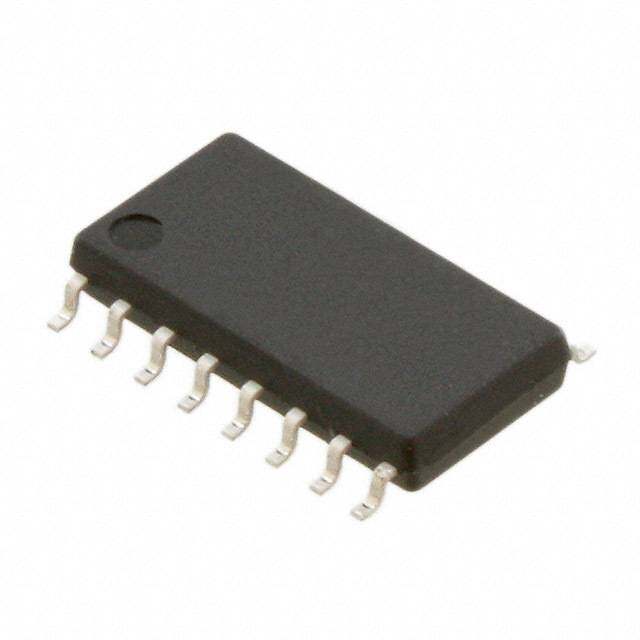
| 描述 | IC SWITCH QUAD SPST 16SOIC模拟开关 IC SWITCH 4X SPST MIX 1 6NSOIC IND |
| 产品分类 | |
| 品牌 | Intersil |
| 产品手册 | |
| 产品图片 |
|
| rohs | 符合RoHS无铅 / 符合限制有害物质指令(RoHS)规范要求 |
| 产品系列 | 开关 IC,模拟开关 IC,Intersil DG413DYZ- |
| 数据手册 | |
| 产品型号 | DG413DYZ |
| PCN组件/产地 | |
| 产品种类 | 模拟开关 IC |
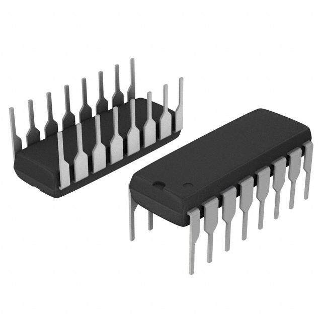
| 供应商器件封装 | 16-SOIC |
| 功能 | |
| 包装 | 管件 |
| 商标 | Intersil |
| 安装类型 | 表面贴装 |
| 安装风格 | SMD/SMT |
| 导通电阻 | 80 欧姆 |
| 导通电阻—最大值 | 45 Ohms |
| 封装 | Tube |
| 封装/外壳 | 16-SOIC(0.154",3.90mm 宽) |
| 封装/箱体 | SOIC-16 |
| 工作温度 | -40°C ~ 85°C |
| 工作电源电压 | 5 V to 44 V |
| 工厂包装数量 | 48 |
| 开关数量 | 4 |
| 开关电压—最大值 | 15 V |
| 开关配置 | SPST |
| 最大双重电源电压 | +/- 20 V |
| 最大工作温度 | + 85 C |
| 最小工作温度 | - 40 C |
| 标准包装 | 48 |
| 电压-电源,单/双 (±) | 5 V ~ 44 V, ±5 V ~ 20 V |
| 电压源 | 单/双电源 |
| 电流-电源 | 100pA |
| 电源电压-最大 | 44 V |
| 电源电压-最小 | 5 V |
| 电源电流 | 0.0001 uA |
| 电源电流—最大值 | 5 uA |
| 电路 | 4 x SPST - NC/NO |
| 空闲时间—最大值 | 140 ns |
| 系列 | DG413 |
| 运行时间—最大值 | 315 ns |


- 商务部:美国ITC正式对集成电路等产品启动337调查
- 曝三星4nm工艺存在良率问题 高通将骁龙8 Gen1或转产台积电
- 太阳诱电将投资9.5亿元在常州建新厂生产MLCC 预计2023年完工
- 英特尔发布欧洲新工厂建设计划 深化IDM 2.0 战略
- 台积电先进制程称霸业界 有大客户加持明年业绩稳了
- 达到5530亿美元!SIA预计今年全球半导体销售额将创下新高
- 英特尔拟将自动驾驶子公司Mobileye上市 估值或超500亿美元
- 三星加码芯片和SET,合并消费电子和移动部门,撤换高东真等 CEO
- 三星电子宣布重大人事变动 还合并消费电子和移动部门
- 海关总署:前11个月进口集成电路产品价值2.52万亿元 增长14.8%


PDF Datasheet 数据手册内容提取
DATASHEET DG411, DG412, DG413 FN3282 Monolithic Quad SPST, CMOS Analog Switches Rev 13.00 June 20, 2007 The DG411 series monolithic CMOS analog switches are Features drop-in replacements for the popular DG211 and DG212 • ON-Resistance (Max). . . . . . . . . . . . . . . . . . . . . . . . . 35 series devices. They include four independent single pole throw (SPST) analog switches, and TTL and CMOS • Low Power Consumption (PD). . . . . . . . . . . . . . . . . . <35µW compatible digital inputs. • Fast Switching Action These switches feature lower analog ON-resistance (<35) - tON (Max) . . . . . . . . . . . . . . . . . . . . . . . . . . . . . . 175ns and faster switch time (tON<175ns) compared to the DG211 - tOFF (Max) . . . . . . . . . . . . . . . . . . . . . . . . . . . . . 145ns or DG212. Charge injection has been reduced, simplifying • Low Charge Injection sample and hold applications. • Upgrade from DG211, DG212 The improvements in the DG411 series are made possible by using a high voltage silicon-gate process. An epitaxial • TTL, CMOS Compatible layer prevents the latch-up associated with older CMOS • Single or Split Supply Operation technologies. The 44V maximum voltage range permits controlling 40VP-P signals. Power supplies may be • Pb-Free Plus Anneal Available (RoHS Compliant) single-ended from +5V to 44V, or split from ±5V to ±20V. Applications The four switches are bilateral, equally matched for AC or bidirectional signals. The ON-resistance variation with analog • Audio Switching signals is quite low over a ±15V analog input range. The • Battery Operated Systems switches in the DG411 and DG412 are identical, differing only • Data Acquisition in the polarity of the selection logic. Two of the switches in the DG413 (#2 and #3) use the logic of the DG211 and DG411 • Hi-Rel Systems (i.e., a logic “0” turns the switch ON) and the other two • Sample and Hold Circuits switches use DG212 and DG412 positive logic. This permits independent control of turn-on and turn-off times for SPDT • Communication Systems configurations, permitting “break-before-make” or “make- • Automatic Test Equipment before-break” operation with a minimum of external logic. FN3282 Rev 13.00 Page 1 of 13 June 20, 2007
DG411, DG412, DG413 Ordering Information PART NUMBER PART MARKING TEMP. RANGE (°C) PACKAGE PKG. DWG. # DG411DJ DG411DJ -40 to +85 16 Ld PDIP E16.3 DG411DJZ (Note) DG411DJZ -40 to +85 16 Ld PDIP** (Pb-free) E16.3 DG411DY* DG411DY -40 to +85 16 Ld SOIC (150 mil) M16.15 DG411DYZ* (Note) DG411DYZ -40 to +85 16 Ld SOIC (150 mil) (Pb-free) M16.15 DG411DVZ* (Note) DG411 DVZ -40 to +85 16 Ld TSSOP (4.4mm) (Pb-free) M16.173 DG412DJ DG412DJ -40 to +85 16 Ld PDIP E16.3 DG412DJZ (Note) DG412DJZ -40 to +85 16 Ld PDIP** (Pb-free) E16.3 DG412DY* DG412DY -40 to +85 16 Ld SOIC (150 mil) M16.15 DG412DYZ* (Note) DG412DYZ -40 to +85 16 Ld SOIC (150 mil) (Pb-free) M16.15 DG412DVZ* (Note) DG412 DVZ -40 to +85 16 Ld TSSOP (4.4mm) (Pb-free) M16.173 DG413DJ DG413DJ -40 to +85 16 Ld PDIP E16.3 DG413DJZ (Note) DG413DJZ -40 to +85 16 Ld PDIP** (Pb-free) E16.3 DG413DY* DG413DY -40 to +85 16 Ld SOIC (150 mil) M16.15 DG413DYZ* (Note) DG413DYZ -40 to +85 16 Ld SOIC (150 mil) (Pb-free) M16.15 DG413DVZ* (Note) DG413 DVZ -40 to +85 16 Ld TSSOP (4.4mm) (Pb-free) M16.173 *Add “-T” suffix for tape and reel. **Pb-free PDIPs can be used for through hole wave solder processing only. They are not intended for use in Reflow solder processing applications. NOTE: Intersil Pb-free plus anneal products employ special Pb-free material sets; molding compounds/die attach materials and 100% matte tin plate termination finish, which are RoHS compliant and compatible with both SnPb and Pb-free soldering operations. Intersil Pb-free products are MSL classified at Pb-free peak reflow temperatures that meet or exceed the Pb-free requirements of IPC/JEDEC J STD-020. Pin Descriptions TRUTH TABLE PIN SYMBOL DESCRIPTION DG411 DG412 DG413 1 IN1 Logic Control for Switch 1. SWITCH SWITCH 2 D1 Drain (Output) Terminal for Switch 1. LOGIC SWITCH SWITCH 1, 4 2, 3 3 S1 Source (Input) Terminal for Switch 1. 0 On Off Off On 4 V- Negative Power Supply Terminal. 1 Off On On Off 5 GND Ground Terminal (Logic Common). NOTE: Logic “0” 0.8V. Logic “1” 2.4V. 6 S4 Source (Input) Terminal for Switch 4. 7 D4 Drain (Output) Terminal for Switch 4. Pinout 8 IN4 Logic Control for Switch 4. 9 IN3 Logic Control for Switch 3. DG411, DG412, DG413 (16 LD PDIP, SOIC, TSSOP) 10 D3 Drain (Output) Terminal for Switch 3. TOP VIEW 11 S3 Source (Input) Terminal for Switch 3. 12 VL Logic Reference Voltage. IN1 1 16 IN2 13 V+ Positive Power Supply Terminal (Substrate). D1 2 15 D2 14 S2 Source (Input) Terminal for Switch 2. S1 3 14 S2 15 D2 Drain (Output) Terminal for Switch 2. V- 4 13 V+ 16 IN2 Logic Control for Switch 2. GND 5 12 VL S4 6 11 S3 D4 7 10 D3 IN4 8 9 IN3 FN3282 Rev 13.00 Page 2 of 13 June 20, 2007
DG411, DG412, DG413 Functional Diagrams Four SPST Switches per Package Switches Shown for Logic “1” Input DG411 DG412 DG413 S1 S1 S1 IN1 IN1 IN1 D1 D1 D1 S2 S2 S2 IN2 IN2 IN2 D2 D2 D2 S3 S3 S3 IN3 IN3 IN3 D3 D3 D3 S4 S4 S4 IN4 IN4 IN4 D4 D4 D4 Schematic Diagram (1 Channel) V+ S V- VL V+ INX D GND V- FN3282 Rev 13.00 Page 3 of 13 June 20, 2007
DG411, DG412, DG413 Absolute Maximum Ratings Thermal Information V+ to V- . . . . . . . . . . . . . . . . . . . . . . . . . . . . . . . . . . . . . . . . . . . 44V Thermal Resistance (Typical, Note 2) JA (°C/W) GND to V-. . . . . . . . . . . . . . . . . . . . . . . . . . . . . . . . . . . . . . . . . . 25V PDIP Package* . . . . . . . . . . . . . . . . . . . . . . . . . . . . 90 VL. . . . . . . . . . . . . . . . . . . . . . . . . . . . . . (GND -0.3V) to (V+) +0.3V SOIC Package. . . . . . . . . . . . . . . . . . . . . . . . . . . . . 110 Digital Inputs, VS, VD (Note 1). . . . . (V-) -2V to (V+) + 2V or 30mA, TSSOP Package . . . . . . . . . . . . . . . . . . . . . . . . . . . 150 Whichever Occurs First Maximum Junction Temperature (Plastic Packages). . . . . . .+150°C Continuous Current (Any Terminal) . . . . . . . . . . . . . . . . . . . . . 30mA Maximum Storage Temperature Range. . . . . . . . . .-65°C to +150°C Peak Current, S or D (Pulsed 1ms, 10% Duty Cycle Max) . . 100mA Pb-free reflow profile . . . . . . . . . . . . . . . . . . . . . . . . . .see link below http://www.intersil.com/pbfree/Pb-FreeReflow.asp Operating Conditions (SOIC and TSSOP - Lead Tips Only) *Pb-free PDIPs can be used for through hole wave solder Voltage Range. . . . . . . . . . . . . . . . . . . . . . . . . . . . . . . . 20V (Max) processing only. They are not intended for use in Reflow solder Temperature Range. . . . . . . . . . . . . . . . . . . . . . . . . .-40°C to +85°C processing applications. Input Low Voltage . . . . . . . . . . . . . . . . . . . . . . . . . . . . . 0.8V (Max) Input High Voltage . . . . . . . . . . . . . . . . . . . . . . . . . . . . . . 2.4V (Min) Input Rise and Fall Time . . . . . . . . . . . . . . . . . . . . . . . . . . . . 20ns CAUTION: Do not operate at or near the maximum ratings listed for extended periods of time. Exposure to such conditions may adversely impact product reliability and result in failures not covered by warranty. NOTES: 1. Signals on SX, DX, or INX exceeding V+ or V- will be clamped by internal diodes. Limit forward diode current to maximum current ratings. 2. JA is measured with the component mounted on a low effective thermal conductivity test board in free air. See Tech Brief TB379 for details. Electrical Specifications Test Conditions: V+ = +15V, V- = -15V, VL = 5V, VIN = 2.4V, 0.8V (Note 3), Unless Otherwise Specified. TEMP MIN TYP MAX PARAMETER TEST CONDITIONS (°C) (Note 4) (Note 5) (Note 4) UNITS DYNAMIC CHARACTERISTICS Turn-ON Time, tON RL = 300, CL = 35pF, VS = 10V (Figure 1) 25 - 110 175 ns 85 - - 220 ns Turn-OFF Time, tOFF 25 - 100 145 ns 85 - - 160 ns Break-Before-Make Time Delay DG413 Only, RL = 300, CL = 35pF (Figure 2) 25 - 25 - ns Charge Injection, Q (Figure 3) CL = 10nF, VG = 0V, RG = 0 25 - 5 - pC OFF Isolation (Figure 5) RL = 50, CL = 5pF, f = 1MHz 25 - 68 - dB Crosstalk (Channel-to-Channel), 25 - -85 - dB (Figure 4) Source OFF Capacitance, CS(OFF) f = 1MHz (Figure 6) 25 - 9 - pF Drain OFF Capacitance, CD(OFF) 25 - 9 - pF Channel ON Capacitance, 25 - 35 - pF CD(ON) + CS(ON) DIGITAL INPUT CHARACTERISTICS Input Current VIN Low, IIL VIN Under Test = 0.8V, All Others = 2.4V Full -0.5 0.005 0.5 A Input Current VIN High, IIH VIN Under Test = 2.4V, All Others = 0.8V Full -0.5 0.005 0.5 A ANALOG SWITCH CHARACTERISTICS Analog Signal Range, VANALOG IS = 10mA Full -15 - 15 V Drain-Source ON Resistance, IS = 10mA, VD = 8.5V, V+ = 13.5V, V- = -13.5V 25 - 25 35 rDS(ON) Full - - 45 FN3282 Rev 13.00 Page 4 of 13 June 20, 2007
DG411, DG412, DG413 Electrical Specifications Test Conditions: V+ = +15V, V- = -15V, VL = 5V, VIN = 2.4V, 0.8V (Note 3), Unless Otherwise Specified. (Continued) TEMP MIN TYP MAX PARAMETER TEST CONDITIONS (°C) (Note 4) (Note 5) (Note 4) UNITS Source OFF Leakage Current, V+ = 16.5V, V- = -16.5V, VD = 15.5V, VS = 15.5V 25 -0.25 0.1 0.25 nA IS(OFF) Full -5 - +5 nA Drain OFF Leakage Current, 25 -0.25 0.1 0.25 nA ID(OFF) Full -5 - +5 nA Channel ON Leakage Current, V+ = 16.5V, V- = -16.5V, VS = VD = 15.5V 25 -0.4 0.1 0.4 nA ID(ON)+ IS(ON) Full -10 - +10 nA POWER SUPPLY CHARACTERISTICS Positive Supply Current, I+ V+ = 16.5V, V- = -16.5V, VIN = 0V or 5V 25 - 0.0001 1 A 85 - - 5 A Negative Supply Current, I- 25 -1 -0.0001 - A 85 -5 - - A Logic Supply Current, IL 25 - 0.0001 1 A 85 - - 5 A Ground Current, IGND 25 -1 -0.0001 - A 85 -5 - - A Electrical Specifications (Single Supply) Test Conditions: V+ = +12V, V- = 0V, VL = 5V, VIN = 2.4V, 0.8V (Note 3), Unless Otherwise Specified. TEMP MIN TYP MAX PARAMETER TEST CONDITIONS (°C) (Note 4) (Note 5) (Note 4) UNITS DYNAMIC CHARACTERISTICS Turn-ON Time, tON RL = 300, CL = 35pF, 25 - 175 250 ns VS = 8V, (Figure 1) 85 - - 315 ns Turn-OFF Time, tOFF 25 - 95 125 ns 85 - - 140 ns Break-Before-Make Time Delay DG413 Only, RL = 300, 25 - 25 - ns CL = 35pF, VS = 8V Charge Injection, Q CL = 10nF, VG = 6.0V, RG = 0 25 - 25 - pC ANALOG SWITCH CHARACTERISTICS Analog Signal Range, VANALOG Full 0 - 12 V Drain-Source ON-Resistance, IS = -10mA, VD = 3V, 8V 25 - 40 80 rDS(ON) V+ = 10.8V Full - - 100 FN3282 Rev 13.00 Page 5 of 13 June 20, 2007
DG411, DG412, DG413 Electrical Specifications (Single Supply) Test Conditions: V+ = +12V, V- = 0V, VL = 5V, VIN = 2.4V, 0.8V (Note 3), Unless Otherwise Specified. (Continued) TEMP MIN TYP MAX PARAMETER TEST CONDITIONS (°C) (Note 4) (Note 5) (Note 4) UNITS POWER SUPPLY CHARACTERISTICS Positive Supply Current, I+ V+ = 13.2V, V- = 0V 25 - 0.0001 1 A VIN = 0V or 5V 85 - - 5 A Negative Supply Current, I- 25 -1 -0.0001 - A 85 -5 - - A Logic Supply Current, IL 25 - 0.0001 1 A 85 - - 5 A Ground Current, IGND 25 -1 -0.0001 - A 85 -5 - - A NOTES: 3. VIN = input voltage to perform proper function. 4. The algebraic convention whereby the most negative value is a minimum and the most positive a maximum, is used in this data sheet. 5. Typical values are for DESIGN AID ONLY, not guaranteed nor subject to production testing. Test Circuits and Waveforms VO is the steady state output with the switch on. Feedthrough via switch capacitance may result in spikes at the leading and trailing edge of the output waveform. +5V +15V LOGIC 3V ttfr << 2200nnss VL V+ SWITCH INPUT 0V 50% SWINITPCUHT S1 D1 OUTPUVTO tOFF IN1 SWITCH INPUT VS LOGIC RL CL VO 90% 90% INPUT V- GND SWITCH OUTPUT 0V -15V tON Repeat test for all IN and S. For load conditions, see Specifications. CL includes fixture and stray NOTE: Logic input waveform is inverted for switches that have the capacitance. V = V ---------------R-----L---------------- opposite logic sense. O S RL+rDSON FIGURE 1A. MEASUREMENTS POINTS FIGURE 1B. TEST CIRCUIT FIGURE 1. SWITCHING TIMES 3V +5V +15V LOGIC VL V+ INPUT 0V S1 D1 VO1 VS1 VS1 = 10V OSUWTITPCUHT 90% S2 D2 VO2 30R0L1 C35Lp1F (V01) VS2 = 10V V0SV2 IN1, IN2 30R0L2 C35Lp2F 90% LOGIC SWITCH INPUT OUTPUT V- VO2 0V GND -15V CL includes fixture and tD tD stray capacitance. FIGURE 2A. MEASUREMENT POINTS FIGURE 2B. TEST CIRCUITS FIGURE 2. BREAK-BEFORE-MAKE TIME FN3282 Rev 13.00 Page 6 of 13 June 20, 2007
DG411, DG412, DG413 Test Circuits and Waveforms (Continued) V+ SWITCH VO OUTPUT RG D1 VO INX OFF ON OFF VG CL V- VIN = 3V ON GND INX OFF Q = VO x CL OFF NOTE: INX dependent on switch configuration, input polarity determined by sense of switch. FIGURE 3A. TEST CIRCUIT FIGURE 3B. MEASUREMENT POINTS FIGURE 3. CHARGE INJECTION +15V C V+ +15V C V+ SGIEGNNEARLATOR 0dBm VS VD 50 GENESRIGATNOARL 0dBm VS 0V, 2.4V IN1 IN2 0V, 2.4V INX 0V, 2.4V ANALYZER VD NC ANALYZER VD RL V- C RL GND V- C GND -15V -15V FIGURE 4. CROSSTALK TEST CIRCUIT FIGURE 5. OFF ISOLATION TEST CIRCUIT +15V C V+ VS INX 0V, 2.4V IMPEDANCE ANALYZER VD f = 1MHz C V- GND -15V FIGURE 6. SOURCE/DRAIN CAPACITANCES TEST CIRCUIT FN3282 Rev 13.00 Page 7 of 13 June 20, 2007
DG411, DG412, DG413 Application Information Summing Amplifier When driving a high impedance, high capacitance load such Single Supply Operation as shown in Figure 7, where the inputs to the summing The DG411, DG412, DG413 can be operated with unipolar amplifier have some noise filtering, it is necessary to have supplies from 5V to 44V. These devices are characterized shunt switches for rapid discharge of the filter capacitor, thus and tested for single supply operation at 12V to facilitate the preventing offsets from occurring at the output. majority of applications. To function properly, 12V is tied to Pins 13 and 0V is tied to Pin 4. Pin 12 still requires 5V for TTL compatible switching. R1 R2 VIN1 C1 R5 R3 R4 VIN2 - VOUT + R6 C2 DG413 FIGURE 7. SUMMING AMPLIFIER FN3282 Rev 13.00 Page 8 of 13 June 20, 2007
DG411, DG412, DG413 Typical Performance Curves 50 240 A: ±5V V+ = 15V, V- = -15V 45 B: ±8V 210 VL = 5V, VS = 10V A C: ±10V 40 D: ±12V 180 35 E: ±15V r ()DS(ON) 322050 F: ±20V BC D E F , t (ns)ONOFF 11529000 tON tOFF t 15 60 10 30 5 TA = +25°C 0 0 -20 -15 -10 -5 0 5 10 15 20 -55 -35 -15 5 25 45 65 85 105 125 DRAIN VOLTAGE (V) TEMPERATURE (°C) FIGURE 8. ON RESISTANCE vs VD AND POWER SUPPLY FIGURE 9. SWITCHING TIME vs TEMPERATURE VOLTAGE 40 100mA V+ = 15V, V- = -15V V+ = 15V, V- = -15V 30 VL = 5V, TA = +25°C VL = 5V 10mA 20 10 ID(OFF) 1mA I+, I- pA) 0 IS(OFF) LY 100A (D -10 PP 4SW I, IS -20 ID(ON) + IS(ON) ISU 10A IL -30 1A 4SW -40 100nA -50 1SW 1SW -60 10nA -15 -10 -5 0 5 10 15 10 100 1k 10k 100k 1M 10M VS, VD (V) FREQUENCY (Hz) FIGURE 10. LEAKAGE CURRENTS vs ANALOG VOLTAGE FIGURE 11. SUPPLY CURRENT vs INPUT SWITCHING FREQUENCY 100 140 V+ = 15V, V- = -15V V+ = 15V, V- = -15V 80 VL = 5V 120 VL = 5V CL = 10nF 100 60 80 CL = 1nF 40 60 C) CL = 10nF C) p 20 p 40 Q ( Q ( 20 0 0 -20 CL = 1nF -20 -40 -40 -60 -60 -15 -10 -5 0 5 10 15 -15 -10 -5 0 5 10 15 VS (V) VD (V) FIGURE 12. CHARGE INJECTION vs SOURCE VOLTAGE FIGURE 13. CHARGE INJECTION vs DRAIN VOLTAGE FN3282 Rev 13.00 Page 9 of 13 June 20, 2007
DG411, DG412, DG413 Die Characteristics DIE DIMENSIONS: PASSIVATION: 2760mm x 1780mm x 485mm Type: Nitride Thickness: 8kÅ ±1kÅ METALLIZATION: WORST CASE CURRENT DENSITY: Type: SiAl Thickness: 12kÅ ±1kÅ 1.5 x 10⁵ A/cm2 Metallization Mask Layout DG411, DG412, DG413 D1 IN1 IN2 (2) (1) (16) (15) D2 S1 (3) (14) S2 (13) V+ SUBSTRATE V- (4) GND (5) (12) VL S4 (6) (11) S3 (7) (8) (9) (10) D4 IN4 IN3 D3 FN3282 Rev 13.00 Page 10 of 13 June 20, 2007
DG411, DG412, DG413 Thin Shrink Small Outline Plastic Packages (TSSOP) M16.173 N 16 LEAD THIN SHRINK SMALL OUTLINE PLASTIC PACKAGE IANRDEEAX E 0.25(0.010) M B M INCHES MILLIMETERS E1 GAUGE SYMBOL MIN MAX MIN MAX NOTES -B- PLANE A - 0.043 - 1.10 - A1 0.002 0.006 0.05 0.15 - 1 2 3 A2 0.033 0.037 0.85 0.95 - L 0.05(0.002) SEATING PLANE 0.25 b 0.0075 0.012 0.19 0.30 9 0.010 -A- c 0.0035 0.008 0.09 0.20 - D A D 0.193 0.201 4.90 5.10 3 -C- E1 0.169 0.177 4.30 4.50 4 e 0.026 BSC 0.65 BSC - e A2 A1 c E 0.246 0.256 6.25 6.50 - b 0.10(0.004) L 0.020 0.028 0.50 0.70 6 0.10(0.004) M C A M B S N 16 16 7 a 0o 8o 0o 8o - NOTES: Rev. 1 2/02 1. These package dimensions are within allowable dimensions of JEDEC MO-153-AB, Issue E. 2. Dimensioning and tolerancing per ANSI Y14.5M-1982. 3. Dimension “D” does not include mold flash, protrusions or gate burrs. Mold flash, protrusion and gate burrs shall not exceed 0.15mm (0.006 inch) per side. 4. Dimension “E1” does not include interlead flash or protrusions. Interlead flash and protrusions shall not exceed 0.15mm (0.006 inch) per side. 5. The chamfer on the body is optional. If it is not present, a visual index feature must be located within the crosshatched area. 6. “L” is the length of terminal for soldering to a substrate. 7. “N” is the number of terminal positions. 8. Terminal numbers are shown for reference only. 9. Dimension “b” does not include dambar protrusion. Allowable dambar protrusion shall be 0.08mm (0.003 inch) total in excess of “b” dimension at maximum material condition. Minimum space between protrusion and adjacent lead is 0.07mm (0.0027 inch). 10. Controlling dimension: MILLIMETER. Converted inch dimen- sions are not necessarily exact. (Angles in degrees) FN3282 Rev 13.00 Page 11 of 13 June 20, 2007
DG411, DG412, DG413 Dual-In-Line Plastic Packages (PDIP) N E16.3 (JEDEC MS-001-BB ISSUE D) E1 16 LEAD DUAL-IN-LINE PLASTIC PACKAGE INDEX AREA 1 2 3 N/2 INCHES MILLIMETERS -B- SYMBOL MIN MAX MIN MAX NOTES -A- A - 0.210 - 5.33 4 D E A1 0.015 - 0.39 - 4 BASE PLANE -C- A2 A A2 0.115 0.195 2.93 4.95 - SEATING B 0.014 0.022 0.356 0.558 - PLANE L CL B1 0.045 0.070 1.15 1.77 8, 10 DB11 e D1 A1 eC eAC C 0.008 0.014 0.204 0.355 - B D 0.735 0.775 18.66 19.68 5 e B 0.010 (0.25) M C A B S D1 0.005 - 0.13 - 5 NOTES: E 0.300 0.325 7.62 8.25 6 1. Controlling Dimensions: INCH. In case of conflict between English and E1 0.240 0.280 6.10 7.11 5 Metric dimensions, the inch dimensions control. e 0.100 BSC 2.54 BSC - 2. Dimensioning and tolerancing per ANSI Y14.5M-1982. 3. Symbols are defined in the “MO Series Symbol List” in Section 2.2 of eA 0.300 BSC 7.62 BSC 6 Publication No. 95. eB - 0.430 - 10.92 7 4. Dimensions A, A1 and L are measured with the package seated in JE- L 0.115 0.150 2.93 3.81 4 DEC seating plane gauge GS-3. N 16 16 9 5. D, D1, and E1 dimensions do not include mold flash or protrusions. Mold flash or protrusions shall not exceed 0.010 inch (0.25mm). Rev. 0 12/93 6. E and eA are measured with the leads constrained to be perpendic- ular to datum -C- . 7. eB and eC are measured at the lead tips with the leads unconstrained. eC must be zero or greater. 8. B1 maximum dimensions do not include dambar protrusions. Dambar protrusions shall not exceed 0.010 inch (0.25mm). 9. N is the maximum number of terminal positions. 10. Corner leads (1, N, N/2 and N/2 + 1) for E8.3, E16.3, E18.3, E28.3, E42.6 will have a B1 dimension of 0.030 - 0.045 inch (0.76 - 1.14mm). FN3282 Rev 13.00 Page 12 of 13 June 20, 2007
DG411, DG412, DG413 Small Outline Plastic Packages (SOIC) N M16.15 (JEDEC MS-012-AC ISSUE C) 16 LEAD NARROW BODY SMALL OUTLINE PLASTIC PACKAGE INDEX AREA H 0.25(0.010) M B M INCHES MILLIMETERS E SYMBOL MIN MAX MIN MAX NOTES -B- A 0.0532 0.0688 1.35 1.75 - 1 2 3 A1 0.0040 0.0098 0.10 0.25 - L B 0.013 0.020 0.33 0.51 9 SEATING PLANE C 0.0075 0.0098 0.19 0.25 - -A- D A h x 45° D 0.3859 0.3937 9.80 10.00 3 E 0.1497 0.1574 3.80 4.00 4 -C- e 0.050 BSC 1.27 BSC - e H 0.2284 0.2440 5.80 6.20 - A1 C h 0.0099 0.0196 0.25 0.50 5 B 0.10(0.004) L 0.016 0.050 0.40 1.27 6 0.25(0.010) M C A M B S N 16 16 7 NOTES: 0° 8° 0° 8° - 1. Symbols are defined in the “MO Series Symbol List” in Section 2.2 of Rev. 1 6/05 Publication Number 95. 2. Dimensioning and tolerancing per ANSI Y14.5M-1982. 3. Dimension “D” does not include mold flash, protrusions or gate burrs. Mold flash, protrusion and gate burrs shall not exceed 0.15mm (0.006 inch) per side. 4. Dimension “E” does not include interlead flash or protrusions. Interlead flash and protrusions shall not exceed 0.25mm (0.010 inch) per side. 5. The chamfer on the body is optional. If it is not present, a visual index feature must be located within the crosshatched area. 6. “L” is the length of terminal for soldering to a substrate. 7. “N” is the number of terminal positions. 8. Terminal numbers are shown for reference only. 9. The lead width “B”, as measured 0.36mm (0.014 inch) or greater above the seating plane, shall not exceed a maximum value of 0.61mm (0.024 inch). 10. Controlling dimension: MILLIMETER. Converted inch dimensions are not necessarily exact. © Copyright Intersil Americas LLC 2002-2007. All Rights Reserved. All trademarks and registered trademarks are the property of their respective owners. For additional products, see www.intersil.com/en/products.html Intersil products are manufactured, assembled and tested utilizing ISO9001 quality systems as noted in the quality certifications found at www.intersil.com/en/support/qualandreliability.html Intersil products are sold by description only. Intersil may modify the circuit design and/or specifications of products at any time without notice, provided that such modification does not, in Intersil's sole judgment, affect the form, fit or function of the product. Accordingly, the reader is cautioned to verify that datasheets are current before placing orders. Information furnished by Intersil is believed to be accurate and reliable. However, no responsibility is assumed by Intersil or its subsidiaries for its use; nor for any infringements of patents or other rights of third parties which may result from its use. No license is granted by implication or otherwise under any patent or patent rights of Intersil or its subsidiaries. For information regarding Intersil Corporation and its products, see www.intersil.com FN3282 Rev 13.00 Page 13 of 13 June 20, 2007