ICGOO在线商城 > 集成电路(IC) > 接口 - 模拟开关,多路复用器,多路分解器 > DG408DJZ

 Datasheet下载
- 型号: DG408DJZ
- 制造商: Intersil
- 库位|库存: xxxx|xxxx
- 要求:
| 数量阶梯 | 香港交货 | 国内含税 |
| +xxxx | $xxxx | ¥xxxx |
查看当月历史价格
查看今年历史价格
DG408DJZ产品简介:
ICGOO电子元器件商城为您提供DG408DJZ由Intersil设计生产,在icgoo商城现货销售,并且可以通过原厂、代理商等渠道进行代购。 DG408DJZ价格参考。IntersilDG408DJZ封装/规格:接口 - 模拟开关,多路复用器,多路分解器, 1 Circuit IC Switch 8:1 100 Ohm 16-PDIP。您可以下载DG408DJZ参考资料、Datasheet数据手册功能说明书,资料中有DG408DJZ 详细功能的应用电路图电压和使用方法及教程。
Renesas Electronics America Inc.生产的DG408DJZ是一款模拟开关、多路复用器和多路分解器,广泛应用于需要信号切换和路由的场景。以下是其主要应用场景:

1. 数据采集系统:DG408DJZ可以用于多通道数据采集系统中,通过选择不同的输入信号通道,将信号传输到ADC(模数转换器)进行处理。这种应用常见于工业控制、医疗设备和环境监测等领域。

2. 音频信号切换:在音频设备中,该芯片可用于切换不同的音频输入源,例如麦克风、线路输入或其他音频设备。这使得音频设备能够灵活地选择信号源,适用于音响系统、耳机放大器等。

3. 测试与测量设备:在测试仪器中,DG408DJZ可以实现对多个测试点的信号切换,方便对不同电路节点进行测量。例如,在示波器或多用表中,它可以快速切换信号通道以提高测试效率。

4. 通信系统:在通信设备中,该芯片可用于信号路径的选择和切换,支持多路信号的传输和处理。例如,在无线通信基站或有线通信网络中,可以用来管理信号的输入输出。

5. 汽车电子:在汽车电子系统中,DG408DJZ可用于传感器信号切换,例如温度传感器、压力传感器等。它可以帮助控制系统从多个传感器中选择合适的信号进行处理,确保车辆运行的安全性和稳定性。

6. 消费电子:在一些消费电子产品中,如家用电器、遥控器等,该芯片可以用于信号的分配和切换,以实现多功能操作。

总之,DG408DJZ凭借其低导通电阻、高带宽和低功耗特性,适合需要高性能信号切换的应用场合,能够满足多种电子系统的信号管理需求。
| 参数 | 数值 |
| 产品目录 | 集成电路 (IC)半导体 |
| 描述 | IC MULTIPLEXER 8X1 16DIP多路器开关 IC MUX 8:1 16PDIP IND |
| 产品分类 | |
| 品牌 | Intersil |
| 产品手册 | |
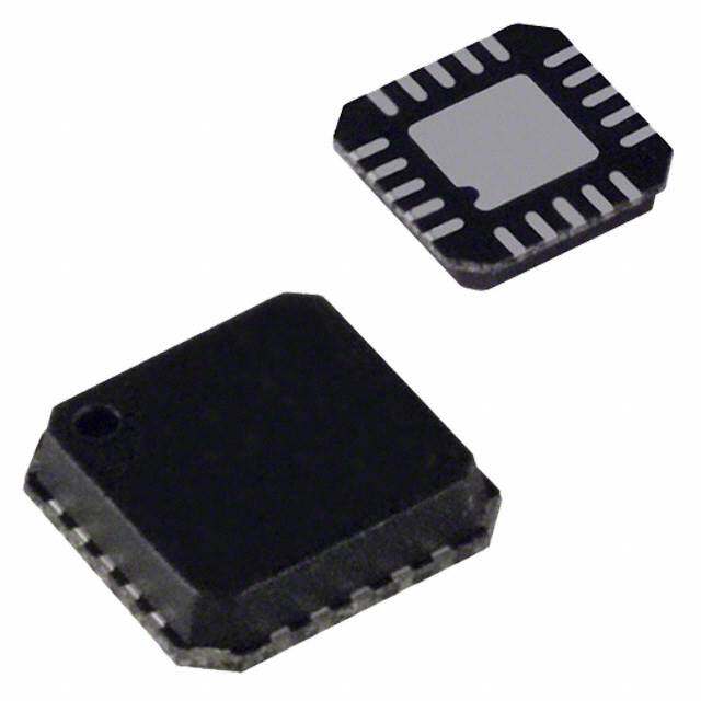
| 产品图片 |
|
| rohs | 符合RoHS无铅 / 符合限制有害物质指令(RoHS)规范要求 |
| 产品系列 | 开关 IC,多路器开关 IC,Intersil DG408DJZ- |
| 数据手册 | |
| 产品型号 | DG408DJZ |
| PCN组件/产地 | |
| 产品目录页面 | |
| 产品种类 | 多路器开关 IC |
| 传播延迟时间 | 250 ns |
| 供应商器件封装 | 16-PDIP |
| 功能 | 多路复用器 |
| 包装 | 管件 |
| 商标 | Intersil |
| 安装类型 | 通孔 |
| 导通电阻 | 100 欧姆 |
| 导通电阻—最大值 | 100 Ohms |
| 封装 | Tube |
| 封装/外壳 | 16-DIP(0.300",7.62mm) |
| 封装/箱体 | PDIP |
| 工作温度 | -40°C ~ 85°C |
| 工作电源电压 | 9 V, 12 V, 15 V, 18 V, 24 V, 28 V |
| 工作电源电流 | +/- 0.5 mA |
| 工厂包装数量 | 25 |
| 开关数量 | 1 |
| 最大工作温度 | + 85 C |
| 最小工作温度 | - 40 C |
| 标准包装 | 25 |
| 电压-电源,单/双 (±) | 5 V ~ 34 V, ±5 V ~ 20 V |
| 电压源 | 单/双电源 |
| 电流-电源 | 200µA |
| 电路 | 1 x 8:1 |
| 空闲时间—最大值 | 120 ns |
| 系列 | DG408 |
| 运行时间—最大值 | 180 ns |
| 通道数量 | 1 Channel |


- 商务部:美国ITC正式对集成电路等产品启动337调查
- 曝三星4nm工艺存在良率问题 高通将骁龙8 Gen1或转产台积电
- 太阳诱电将投资9.5亿元在常州建新厂生产MLCC 预计2023年完工
- 英特尔发布欧洲新工厂建设计划 深化IDM 2.0 战略
- 台积电先进制程称霸业界 有大客户加持明年业绩稳了
- 达到5530亿美元!SIA预计今年全球半导体销售额将创下新高
- 英特尔拟将自动驾驶子公司Mobileye上市 估值或超500亿美元
- 三星加码芯片和SET,合并消费电子和移动部门,撤换高东真等 CEO
- 三星电子宣布重大人事变动 还合并消费电子和移动部门
- 海关总署:前11个月进口集成电路产品价值2.52万亿元 增长14.8%


PDF Datasheet 数据手册内容提取
DATASHEET DG408, DG409 FN3283 Single 8-Channel/Differential 4-Channel, CMOS Analog Multiplexers Rev 8.00 Jun 13, 2006 The DG408 Single 8-Channel, and DG409 Differential Features 4-Channel monolithic CMOS analog multiplexers are drop-in • ON Resistance (Max, 25°C). . . . . . . . . . . . . . . . . . . 100 replacements for the popular DG508A and DG509A series devices. They each include an array of eight analog • Low Power Consumption (PD) . . . . . . . . . . . . . . .<11mW switches, a TTL/CMOS compatible digital decode circuit for • Fast Switching Action channel selection, a voltage reference for logic thresholds and an ENABLE input for device selection when several - tTRANS . . . . . . . . . . . . . . . . . . . . . . . . . . . . . . . .<250ns multiplexers are present. - tON/OFF(EN) . . . . . . . . . . . . . . . . . . . . . . . . . . . .<150ns • Low Charge Injection The DG408 and DG409 feature lower signal ON resistance (<100) and faster switch transition time (tTRANS < 250ns) • Upgrade from DG508A/DG509A compared to the DG508A or DG509A. Charge injection has • TTL, CMOS Compatible been reduced, simplifying sample and hold applications. The improvements in the DG408 series are made possible by • Single or Split Supply Operation using a high-voltage silicon-gate process. An epitaxial layer • Pb-Free Plus Anneal Available (RoHS Compliant) prevents the latch-up associated with older CMOS technologies. Power supplies may be single-ended from +5V Applications to +34V, or split from 5V to 20V. • Data Acquisition Systems The analog switches are bilateral, equally matched for AC or • Audio Switching Systems bidirectional signals. The ON resistance variation with analog signals is quite low over a 5V analog input range. • Automatic Testers • Hi-Rel Systems • Sample and Hold Circuits • Communication Systems • Analog Selector Switch Ordering Information PART PART TEMP. PKG. NUMBER MARKING RANGE (°C) PACKAGE DWG. # DG408DJ DG408DJ -40 to 85 16 Ld PDIP E16.3 DG408DJZ (Note) DG408DJZ -40 to 85 16 Ld PDIP** (Pb-free) E16.3 DG408DY* DG408DY -40 to 85 16 Ld SOIC M16.15 DG408DYZ* (Note) DG408DYZ -40 to 85 16 Ld SOIC (Pb-free) M16.15 DG408DVZ* (Note) DG408DVZ -40 to 85 16 Ld TSSOP (Pb-free) M16.173 DG409DJ DG409DJ -40 to 85 16 Ld PDIP E16.3 DG409DJZ (Note) DG409DJZ -40 to 85 16 Ld PDIP** (Pb-free) E16.3 DG409DY* DG409DY -40 to 85 16 Ld SOIC M16.15 DG409DYZ* (Note) DG409DYZ -40 to 85 16 Ld SOIC (Pb-free) M16.15 DG409DVZ* (Note) DG409DVZ -40 to 85 16 Ld TSSOP (Pb-free) M16.173 *Add “-T” suffix for tape and reel. **Pb-free PDIPs can be used for through hole wave solder processing only. They are not intended for use in Reflow solder processing applications. NOTE: Intersil Pb-free plus anneal products employ special Pb-free material sets; molding compounds/die attach materials and 100% matte tin plate termination finish, which are RoHS compliant and compatible with both SnPb and Pb-free soldering operations. Intersil Pb-free products are MSL classified at Pb-free peak reflow temperatures that meet or exceed the Pb-free requirements of IPC/JEDEC J STD-020. FN3283 Rev 8.00 Page 1 of 17 Jun 13, 2006
DG408, DG409 Pinouts DG408 (PDIP, SOIC, TSSOP) DG409 (PDIP, SOIC, TSSOP) TOP VIEW TOP VIEW A0 1 16 A1 A0 1 16 A1 EN 2 15 A2 EN 2 15 GND V- 3 14 GND V- 3 14 V+ S1 4 13 V+ S1A 4 13 S1B S2 5 12 S5 S2A 5 12 S2B S3 6 11 S6 S3A 6 11 S3B S4 7 10 S7 S4A 7 10 S4B D 8 9 S8 DA 8 9 DB Functional Block Diagrams DG408 DG409 S1 D S1A DA S2 S4A DECODER/ DRIVER S1B DB S8 S4B DEDCROIVDEERR/ 5V LEVEL 5V LEVEL REF SHIFT REF SHIFT †DIGITAL † † † † †DIGITAL † † † INPUT INPUT PROTECTION PROTECTION A0 A1 A2 EN A0 A1 EN TRUTH TABLE DG408 TRUTH TABLE DG409 A2 A1 A0 EN ON SWITCH A1 A0 EN ON SWITCH X X X 0 NONE X X 0 NONE 0 0 0 1 1 0 0 1 1 0 0 1 1 2 0 1 1 2 0 1 0 1 3 1 0 1 3 0 1 1 1 4 1 1 1 4 1 0 0 1 5 NOTES: 1 0 1 1 6 1. VAH Logic “1”2.4V. 2. VAL Logic “0” 0.8V. 1 1 0 1 7 1 1 1 1 8 FN3283 Rev 8.00 Page 2 of 17 Jun 13, 2006
DG408, DG409 Pin Descriptions - (DG408) Pin Descriptions - (DG409) PIN SYMBOL DESCRIPTION PIN SYMBOL DESCRIPTION 1 A0 Logic Decode Input (Bit 0, LSB) 1 A0 Logic Decode Input (Bit 0, LSB) 2 EN Enable Input 2 EN Enable Input 3 V- Negative Power Supply Terminal 3 V- Negative Power Supply Terminal 4 S1 Source (Input) for Channel 1 4 S1A Source (Input) for Channel 1a 5 S2 Source (Input) for Channel 2 5 S2A Source (Input) for Channel 2a 6 S3 Source (Input) for Channel 3 6 S3A Source (Input) for Channel 3a 7 S4 Source (Input) for Channel 4 7 S4A Source (Input) for Channel 4a 8 D Drain (Output) 8 DA Drain a (Output a) 9 S8 Source (Input) for Channel 8 9 DB Drain b (Output b) 10 S7 Source (Input) for Channel 7 10 S4B Source (Input) for Channel 4b 11 S6 Source (Input) for Channel 6 11 S3B Source (Input) for Channel 3b 12 S5 Source (Input) for Channel 5 12 S2B Source (Input) for Channel 2b 13 V+ Positive Power Supply Terminal (Substrate) 13 S1B Source (Input) for Channel 1b 14 GND Ground Terminal (Logic Common) 14 V+ Positive Power Supply Terminal 15 A2 Logic Decode Input (Bit 2, MSB) 15 GND Ground Terminal (Logic Common) 16 A1 Logic Decode Input (Bit 1) 16 A1 Logic Decode Input (Bit 1, MSB) FN3283 Rev 8.00 Page 3 of 17 Jun 13, 2006
DG408, DG409 Absolute Maximum Ratings Thermal Information V+ to V- . . . . . . . . . . . . . . . . . . . . . . . . . . . . . . . . . . . . . . . . . . 44.0V Thermal Resistance (Typical, Note 4) JA (°C/W) GND to V-. . . . . . . . . . . . . . . . . . . . . . . . . . . . . . . . . . . . . . . . . . .25V PDIP Package . . . . . . . . . . . . . . . . . . . . . . . . . . . . . 90 Digital Inputs, VS, VD (Note 3). . . . . .(V-) -2V to (V+) + 2V or 20mA, SOIC Package. . . . . . . . . . . . . . . . . . . . . . . . . . . . . 110 Whichever Occurs First TSSOP Package . . . . . . . . . . . . . . . . . . . . . . . . . . . 150 Continuous Current (Any Terminal) . . . . . . . . . . . . . . . . . . . . . 30mA Maximum Junction Temperature . . . . . . . . . . . . . . . . . . . . . . .150°C Peak Current, S or D (Pulsed 1ms, 10% Duty Cycle Max) . . 100mA Maximum Storage Temperature Range. . . . . . . . . . -65°C to 125°C Maximum Lead Temperature (Soldering 10s) . . . . . . . . . . . . .300°C Operating Conditions (SOIC and TSSOP - Lead Tips Only) Temperature Range. . . . . . . . . . . . . . . . . . . . . . . . . . -40°C to 85°C CAUTION: Stresses above those listed in “Absolute Maximum Ratings” may cause permanent damage to the device. This is a stress only rating and operation of the device at these or any other conditions above those indicated in the operational sections of this specification is not implied. NOTES: 3. Signals on SX, DX, EN or AX exceeding V+ or V- are clamped by internal diodes. Limit diode current to maximum current ratings. 4. JA is measured with the component mounted on an evaluation PC board in free air. Electrical Specifications Test Conditions: V+ = +15V, V- = -15V, VAL = 0.8V, VAH = 2.4V, Unless Otherwise Specified (NOTE 5) (NOTE 6) (NOTE 5) PARAMETER TEST CONDITIONS TEMP (°C) MIN TYP MAX UNITS DYNAMIC CHARACTERISTICS Transition Time, tTRANS (See Figure 1) Full - 160 250 ns Break-Before-Make Interval, tOPEN (See Figure 3) 25 10 - - ns Enable Turn-ON Time, tON(EN) (See Figure 2) 25 - 115 150 ns Full - - 225 ns Enable Turn-OFF Time, tOFF(EN) (See Figure 2) Full - 105 150 ns Charge Injection, Q CL = 10nF, VS = 0V 25 - 20 - pC OFF Isolation VEN = 0V, RL = 1k, 25 - -75 - dB f = 100kHz (Note 9) Logic Input Capacitance, CIN f = 1MHz 25 - 8 - pF Source OFF Capacitance, CS(OFF) VEN = 0V, VS = 0V, 25 - 3 - pF f = 1MHz Drain OFF Capacitance, CD(OFF) VEN = 0V, VD = 0V, DG408 f = 1MHz 25 - 26 - pF DG409 25 - 14 - pF Drain ON Capacitance, CD(ON) VEN = 3V, VD = 0V, DG408 f = 1MHz, VA = 0V or 3V 25 - 37 - pF DG409 25 - 25 - pF DIGITAL INPUT CHARACTERISTICS Logic Input Current, VA = 2.4V, 15V Full -10 - 10 A Input Voltage High, IAH Logic Input Current, VEN = 0V, 2.4V, Full -10 - 10 A Input Voltage Low, IAL VA = 0V ANALOG SWITCH CHARACTERISTICS Analog Signal Range, VANALOG Full -15 - 15 V Drain-Source ON Resistance, VD = 10V, IS = -10mA 25 - 40 100 rDS(ON) (Note 7) Full - - 125 rDS(ON) Matching Between Channels, VD = 10V, -10V (Note 8) 25 - - 15 rDS(ON) Source OFF Leakage Current, IS(OFF) VEN = 0V, VS = 10V, 25 -0.5 - 0.5 nA VD = +10V Full -5 - 5 nA FN3283 Rev 8.00 Page 4 of 17 Jun 13, 2006
DG408, DG409 Electrical Specifications Test Conditions: V+ = +15V, V- = -15V, VAL = 0.8V, VAH = 2.4V, Unless Otherwise Specified (Continued) (NOTE 5) (NOTE 6) (NOTE 5) PARAMETER TEST CONDITIONS TEMP (°C) MIN TYP MAX UNITS Drain OFF Leakage Current, ID(OFF) VEN = 0V, VD = 10V, DG408 VS = +10V 25 -1 - 1 nA Full -20 - 20 nA DG409 25 -1 - 1 nA Full -10 - 10 nA Drain ON Leakage Current, ID(ON) VS = VD = 10V (Note 7) DG408 25 -1 - 1 nA Full -20 - 20 nA DG409 25 -1 - 1 nA Full -10 - 10 nA POWER SUPPLY CHARACTERISTICS Positive Supply Current, I+ VEN = 0V, VA = 0V (Standby) Full - 10 75 A Negative Supply Current, I- Full -75 1 - A Positive Supply Current, I+ VEN = 2.4V, VA = 0V 25 - 0.2 0.5 mA (Enabled) Full - - 2 mA Negative Supply Current, I- Full -500 - - A Electrical Specifications Single Supply Test Conditions: V+ = 12V, V- = 0V, VAL = 0.8V, VAH = 2.4V, Unless Otherwise Specified TEST (NOTE 5) (NOTE 6) (NOTE 5) PARAMETER CONDITION TEMP (°C) MIN TYP MAX UNITS DYNAMIC CHARACTERISTICS Switching Time of Multiplexer, tTRANS VS1 = 8V, VS8 = 0V, VIN = 2.4V 25 - 180 - ns Enable Turn-ON Time, tON(EN) VINH = 2.4V, VINL = 0V, 25 - 180 - ns VS1 = 5V Enable Turn-OFF Time, tOFF(EN) 25 - 120 - ns Charge Injection, Q CL = 10nF, VGEN = 0V, 25 - 5 - pC RGEN = 0 ANALOG SWITCH CHARACTERISTICS Analog Signal Range, VANALOG Full 0 - 12 V Drain-Source ON-Resistance, VD = 3V, 10V, IS = -1mA 25 - 90 - rDS(ON) (Note 7) NOTES: 5. The algebraic convention whereby the most negative value is a minimum and the most positive a maximum, is used in this data sheet. 6. Typical values are for DESIGN AID ONLY, not guaranteed nor production tested. 7. Sequence each switch ON. 8. rDS(ON) = rDS(ON) (Max) - rDS(ON) (Min). 9. Worst case isolation occurs on channel 4 due to proximity to the drain pin. FN3283 Rev 8.00 Page 5 of 17 Jun 13, 2006
DG408, DG409 Test Circuits and Waveforms +15V +15V +2.4V +2.4V EN V+ S1 10V EN V+S1B 10V A0 S2 - S7 S1A - S4A, DA LINOPGUICT A1 DG408 S8 10V SOWUTITPCUHT LINOPGUICT A0 DG409 S4B 10V SOWUTITPCUHT A2GND V- D VO A1GND V- DB VO 50 300 35pF 50 300 35pF -15V -15V FIGURE 1A. DG408 TEST CIRCUIT FIGURE 1B. DG409 TEST CIRCUIT tr < 20ns tf < 20ns 3V LOGIC 50% 50% INPUT 0V S1 ON VS1 SWITCH 0.8 VS1 OUTPUT 0V VO 0.8 VS8 VS8 tTRANS tTRANS S8 ON FIGURE 1C. MEASUREMENT POINTS FIGURE 1. TRANSITION TIME +15V +15V V+ V+ A0 S1 -5V A0 S1B -5V DG408 DG409 LOGIC A1 S2 - S8 SWITCH LOGIC A1 S1A - S4A SWITCH INPUT VIN EAN2GND V- D OUTPUVTO INPUT VIN ENGS2NBD - S4VB-, DDBA OUTPUVTo 50 300 35pF 50 300 35pF -15V -15V FIGURE 2A. DG408 TEST CIRCUIT FIGURE 2B. DG409 TEST CIRCUIT tr < 20ns 3V tf < 20ns LOGIC 50% 50% INPUT VIN 0V tON(EN) 0V SWITCH OUTPUT VO 0.9 VO VO tOFF(EN) FIGURE 2C. MEASUREMENT POINTS FIGURE 2. ENABLE SWITCHING TIMES FN3283 Rev 8.00 Page 6 of 17 Jun 13, 2006
DG408, DG409 Test Circuits and Waveforms (Continued) +15V tr < 20ns 3V tf < 20ns +2.4V LOGIC INPUT V+ 0V EN ALL S AND DA +5V (VS) A0 DG408 VS LINOPGUICT A1 DG409 SOWUTITPCUHT OSUWTITPCUHT 80% 80% A2GND V-D, DB VO VO 50 300 35pF 0V -15V tOPEN FIGURE 3A. TEST CIRCUIT FIGURE 3B. MEASUREMENT POINTS FIGURE 3. BREAK-BEFORE-MAKE INTERVAL +15V 3V LOGIC RGEN V+ INPUT 0V SX D VO VGEN CHANNEL A0 CL SELECT AA12 10nF OSUWTITPCUHT ON OFF VO EN GND V- VO IS THE MEASURED VOLTAGE DUE TO CHARGE TRANSFER ERROR, Q LOGIC INPUT -15V Q = CL xVO FIGURE 4A. TEST CIRCUIT FIGURE 4B. MEASUREMENT POINTS FIGURE 4. CHARGE INJECTION 5V +15V 0V +15V VIN S1 EN V+ S|X EN V+ 1k VIN SX | VO || VO S8 D S8 D GESNIEGRNAATLOR AAA210 V- 1k GESNIEGRNAATLOR AAA210 V- 1k GND GND -15V -15V ANALYZER ANALYZER V OFFISOLATION = 20Log-----O-----U-----T-- VOUT V CROSSTALK = 20Log----------------- IN V IN FIGURE 5. OFF ISOLATION FIGURE 6. CROSSTALK FN3283 Rev 8.00 Page 7 of 17 Jun 13, 2006
DG408, DG409 Test Circuits and Waveforms (Continued) 5V +15V 3V OR 0V +15V VIN S1 EN V+ EN V+ A2 S1 VO | D CHANNEL | SELECT A1 S8 GESNIEGRNAATLOR AAA210 RL A0 D IMANPEADLYAZNECRE V- V- GND GND -15V -15V ANALYZER V OUT INSERTIONLOSS = 20Log----------------- V IN FIGURE 7. INSERTION LOSS FIGURE 8. SOURCE/DRAIN CAPACITANCES Typical Applications Overvoltage Protection V+ A very convenient form of overvoltage protection consists of adding two small signal diodes (1N4148, 1N914 type) in 1N4148 series with the supply pins (see Figure 9). This arrangement effectively blocks the flow of reverse currents. It also floats the supply pin above or below the normal V+ or V- value. In this case the overvoltage signal actually becomes the power SX D supply of the IC. From the point of view of the chip, nothing has changed, as long as the difference V+ - (V-) doesn’t DG408 exceed 44V. The addition of these diodes will reduce the VG analog signal range to 1V below V+ and 1V above V-, but it 1N4148 preserves the low channel resistance and low leakage characteristics. V- Typical application information is for Design Aid Only, not FIGURE 9. OVERVOLTAGE PROTECTION USING BLOCKING guaranteed and not subject to production testing. DIODES FN3283 Rev 8.00 Page 8 of 17 Jun 13, 2006
DG408, DG409 Typical Performance Curves 3.5 75 3.0 CD(ON) V+ = +15V V- = -15V 2.0 50 F) I (pA)IN 1.0 C (pS, D CD(OFF) 0.5pA 25 0.0 CS(OFF) -1.0 0 0 5 10 15 0 4 8 12 VIN (V) VA (V) FIGURE 10. INPUT LOGIC CURRENT vs LOGIC INPUT FIGURE 11. SOURCE/DRAIN CAPACITANCE vs ANALOG VOLTAGE VOLTAGE (SINGLE 12V SUPPLY) 80 VSUPPLY = 15V V+ = +15V VIN = 0V V- = -15V 0 60 CD(ON) pF) CD(OFF) A) -200 C (S, D 40 I (pIN -400 20 CS(OFF) -600 0 -800 -15 0 15 -55 5 45 85 125 VA (V) TEMPERATURE (°C) FIGURE 12. SOURCE/DRAIN CAPACITANCE vs ANALOG FIGURE 13. LOGIC INPUT CURRENT vs TEMPERATURE VOLTAGE 60 100 V+ = 15V 40 DG408 ID(OFF) 60 V- = -15V DG409 ID(OFF) VS = -VD FOR ID(OFF) DG409 ID(ON) VD = VS(OPEN) FOR ID(ON) 20 20 DG408 ID(ON) A) A) (pD 0 (pD -20 I I -60 -20 DG409 ID(OFF) -40 VS = 0V FOR ID(OFF) -100 DG409 ID(ON) VS = VD FOR ID(ON) DG408 ID(ON), ID(OFF) -60 -140 0 2 4 6 8 10 12 -15 0 15 VD (V) VS, VD (V) FIGURE 14. DRAIN LEAKAGE CURRENT vs SOURCE/DRAIN FIGURE 15. DRAIN LEAKAGE CURRENT vs SOURCE/DRAIN VOLTAGE (SINGLE 12V SUPPLY) VOLTAGE FN3283 Rev 8.00 Page 9 of 17 Jun 13, 2006
DG408, DG409 Typical Performance Curves (Continued) 20 2.0 15 1.5 V+ = +15V 10 V- = -15V A) (pF) 5 (V)N 1.0 OF VI S( I 0 V+ = +12V 0.5 V- = 0V -5 -10 0.0 -15 0 15 4 8 12 16 20 VS (V) VSUPPLY (V) FIGURE 16. SOURCE LEAKAGE CURRENT vs SOURCE FIGURE 17. INPUT SWITCHING THRESHOLD vs SUPPLY VOLTAGE VOLTAGE 105 104 VSUPPLY = 15V VSUPPLY = 15V 104 103 EN = 2.4V 103 102 A) A) -(I-) ( 102 I+ (m 10 EN = 0V 10 1 EN = 2.4V 1 0.1 EN = 0V 0.1 0.01 100 1K 10K 100K 1M 10M 100 1k 10k 100k 1M 10M SWITCHING FREQUENCY (Hz) SWITCHING FREQUENCY (Hz) FIGURE 18. NEGATIVE SUPPLY CURRENT vs SWITCHING FIGURE 19. POSITIVE SUPPLY CURRENT vs SWITCHING FREQUENCY FREQUENCY 105 VSUPPLY = 15V 0 104 I+ 103 -200 +, I- (nA) 11002 I- (nA) -400 I V+ = 15V 1 V- = -15V -600 VIN = 0V 0.1 VEN = 0V -(I-) 0.01 -800 -55 5 45 85 125 -55 5 45 85 125 TEMPERATURE (°C) TEMPERATURE (°C) FIGURE 20. ISUPPLY vs TEMPERATURE FIGURE 21. NEGATIVE SUPPLY CURRENT vs TEMPERATURE FN3283 Rev 8.00 Page 10 of 17 Jun 13, 2006
DG408, DG409 Typical Performance Curves (Continued) 90 20 80 CL = 10,000pF V+ = 15V VIN = 5VP-P V- = -15V 70 VIN = 0V 60 15 VEN = 0V V+ = 15V 50 V- = -15V I+ (A) 10 Q (pC) 4300 20 5 10 V+ = 12V 0 V- = 0V -10 0 -15 -10 -5 0 5 10 15 -55 5 45 85 125 VS (V) TEMPERATURE (°C) FIGURE 22. POSITIVE SUPPLY CURRENT vs TEMPERATURE FIGURE 23. CHARGE INJECTION vs ANALOG VOLTAGE (DG408) 120 160 140 100 V+ = 7.5V 5V 120 80 ) ) 100 10V (DS(ON) 60 8V10V12V (DS(ON) 80 12V 15V r r 60 20V 40 40 22V 15V V- = 0V 20 20 20V 0 0 -20 -16 -12 -8 -4 0 4 8 12 16 20 0 4 8 12 16 20 22 VD (V) VD (V) FIGURE 24. rDS(ON) vs VD AND SUPPLY FIGURE 25. rDS(ON) vs VD (SINGLE SUPPLY) 80 130 V+ = 15V 125°C 70 V- = -15V 110 60 85°C 125°C 90 50 ()ON) 40 85°C ()ON) 70 25°C S( 25°C S( D D r 30 r 50 20 0°C 0°C 10 -40°C 30 -40°C V+ = 12V -55°C V- = 0V -55°C 0 10 -15 0 15 0 4 8 12 VS (V) VS (V) FIGURE 26. rDS(ON) vs VS AND TEMPERATURE FIGURE 27. rDS(ON) vs VS AND TEMPERATURE (SINGLE SUPPLY) FN3283 Rev 8.00 Page 11 of 17 Jun 13, 2006
DG408, DG409 Typical Performance Curves (Continued) -150 275 V+ = +15V -130 V- = -15V 250 RL = 1k 225 -110 (dB) -90 OFF ISOLATION t(ns) 210705 tTRANS -70 tOFF(EN) 150 -50 CROSSTALK 125 tON(EN) -30 100 100 1k 10k 100k 1M 10M 100M 8 9 10 11 12 13 14 15 FREQUENCY (Hz) VSUPPLY (V) FIGURE 28. OFF ISOLATION AND CROSSTALK vs FREQUENCY FIGURE 29. SWITCHING TIME vs SINGLE SUPPLY 200 190 tTRANS tTRANS 175 170 150 150 tON(EN) s) s) n n t ( t ( 125 130 tOFF(EN) 100 110 tOFF(EN) tON(EN) 75 90 10 12 14 16 18 20 22 2 3 4 5 VSUPPLY (V) VIN (V) FIGURE 30. SWITCHING TIME vs BIPOLAR SUPPLY FIGURE 31. SWITCHING TIME vs VIN (SINGLE SUPPLY) 180 1 RL = 1k tTRANS 0 160 -1 V+ = +15V V- = -15V 140 B) -2 REF. 1VRMS t (ns) OSS (d -3 120 L tOFF(EN) -4 100 -5 RL = 50 tON(EN) 80 -6 2 3 4 5 10 102 103 104 105 106 107 108 VIN (V) FREQUENCY (Hz) FIGURE 32. SWITCHING TIME vs VIN (BIPOLAR SUPPLY) FIGURE 33. INSERTION LOSS vs FREQUENCY FN3283 Rev 8.00 Page 12 of 17 Jun 13, 2006
DG408, DG409 Die Characteristics DIE DIMENSIONS: PASSIVATION: 1800m x 3320m x 485m Type: Nitride Thickness: 8kÅ 1kÅ METALLIZATION: WORST CASE CURRENT DENSITY: Type: SiAl Thickness: 12kÅ 1kÅ 9.1 x 10⁴ A/cm2 Metallization Mask Layout DG408 EN A0 A1 A2 GND (2) (1) (16) (15) (14) NC V- (3) (13) V+ S1 (4) (12) S5 S2 (5) (11) S6 S3 (6) NC S4 (7) (8) (9) (10) D S8 S7 FN3283 Rev 8.00 Page 13 of 17 Jun 13, 2006
DG408, DG409 Die Characteristics DIE DIMENSIONS: PASSIVATION: 1800m x 3320m x 485m Type: Nitride Thickness: 8kÅ 1kÅ METALLIZATION: WORST CASE CURRENT DENSITY: Type: SiAl Thickness: 12kÅ 1kÅ 9.1 x 10⁴ A/cm2 Metallization Mask Layout DG409 EN A0 A1 GND (2) (1) (16) NC (15) NC V- (3) (14) V+ S1A (4) (13) S1B S2A (5) (12) S2B S3A (6) (11) S3B S4A (7) (8) (9) (10) DA DB S4B FN3283 Rev 8.00 Page 14 of 17 Jun 13, 2006
DG408, DG409 Thin Shrink Small Outline Plastic Packages (TSSOP) M16.173 N 16 LEAD THIN SHRINK SMALL OUTLINE PLASTIC PACKAGE IANRDEEAX E 0.25(0.010) M B M INCHES MILLIMETERS E1 GAUGE SYMBOL MIN MAX MIN MAX NOTES -B- PLANE A - 0.043 - 1.10 - A1 0.002 0.006 0.05 0.15 - 1 2 3 A2 0.033 0.037 0.85 0.95 - L 0.05(0.002) SEATING PLANE 0.25 b 0.0075 0.012 0.19 0.30 9 0.010 -A- c 0.0035 0.008 0.09 0.20 - D A D 0.193 0.201 4.90 5.10 3 -C- E1 0.169 0.177 4.30 4.50 4 e 0.026 BSC 0.65 BSC - e A2 A1 c E 0.246 0.256 6.25 6.50 - b 0.10(0.004) L 0.020 0.028 0.50 0.70 6 0.10(0.004) M C A M B S N 16 16 7 0o 8o 0o 8o - NOTES: Rev. 1 2/02 1. These package dimensions are within allowable dimensions of JEDEC MO-153-AB, Issue E. 2. Dimensioning and tolerancing per ANSI Y14.5M-1982. 3. Dimension “D” does not include mold flash, protrusions or gate burrs. Mold flash, protrusion and gate burrs shall not exceed 0.15mm (0.006 inch) per side. 4. Dimension “E1” does not include interlead flash or protrusions. Interlead flash and protrusions shall not exceed 0.15mm (0.006 inch) per side. 5. The chamfer on the body is optional. If it is not present, a visual index feature must be located within the crosshatched area. 6. “L” is the length of terminal for soldering to a substrate. 7. “N” is the number of terminal positions. 8. Terminal numbers are shown for reference only. 9. Dimension “b” does not include dambar protrusion. Allowable dambar protrusion shall be 0.08mm (0.003 inch) total in excess of “b” dimension at maximum material condition. Minimum space between protrusion and adjacent lead is 0.07mm (0.0027 inch). 10. Controlling dimension: MILLIMETER. Converted inch dimen- sions are not necessarily exact. (Angles in degrees) FN3283 Rev 8.00 Page 15 of 17 Jun 13, 2006
DG408, DG409 Dual-In-Line Plastic Packages (PDIP) N E16.3 (JEDEC MS-001-BB ISSUE D) E1 16 LEAD DUAL-IN-LINE PLASTIC PACKAGE INDEX AREA 1 2 3 N/2 INCHES MILLIMETERS -B- SYMBOL MIN MAX MIN MAX NOTES -A- A - 0.210 - 5.33 4 D E A1 0.015 - 0.39 - 4 BASE PLANE -C- A2 A A2 0.115 0.195 2.93 4.95 - SEATING B 0.014 0.022 0.356 0.558 - PLANE L CL B1 0.045 0.070 1.15 1.77 8, 10 DB11 e D1 A1 eC eAC C 0.008 0.014 0.204 0.355 - B D 0.735 0.775 18.66 19.68 5 e B 0.010 (0.25) M C A B S D1 0.005 - 0.13 - 5 NOTES: E 0.300 0.325 7.62 8.25 6 1. Controlling Dimensions: INCH. In case of conflict between English and E1 0.240 0.280 6.10 7.11 5 Metric dimensions, the inch dimensions control. e 0.100 BSC 2.54 BSC - 2. Dimensioning and tolerancing per ANSI Y14.5M-1982. 3. Symbols are defined in the “MO Series Symbol List” in Section 2.2 of eA 0.300 BSC 7.62 BSC 6 Publication No. 95. eB - 0.430 - 10.92 7 4. Dimensions A, A1 and L are measured with the package seated in JE- L 0.115 0.150 2.93 3.81 4 DEC seating plane gauge GS-3. N 16 16 9 5. D, D1, and E1 dimensions do not include mold flash or protrusions. Mold flash or protrusions shall not exceed 0.010 inch (0.25mm). Rev. 0 12/93 6. E and eA are measured with the leads constrained to be perpendic- ular to datum -C- . 7. eB and eC are measured at the lead tips with the leads unconstrained. eC must be zero or greater. 8. B1 maximum dimensions do not include dambar protrusions. Dambar protrusions shall not exceed 0.010 inch (0.25mm). 9. N is the maximum number of terminal positions. 10. Corner leads (1, N, N/2 and N/2 + 1) for E8.3, E16.3, E18.3, E28.3, E42.6 will have a B1 dimension of 0.030 - 0.045 inch (0.76 - 1.14mm). FN3283 Rev 8.00 Page 16 of 17 Jun 13, 2006
DG408, DG409 Small Outline Plastic Packages (SOIC) N M16.15 (JEDEC MS-012-AC ISSUE C) 16 LEAD NARROW BODY SMALL OUTLINE PLASTIC PACKAGE INDEX AREA H 0.25(0.010) M B M INCHES MILLIMETERS E SYMBOL MIN MAX MIN MAX NOTES -B- A 0.0532 0.0688 1.35 1.75 - 1 2 3 A1 0.0040 0.0098 0.10 0.25 - L B 0.013 0.020 0.33 0.51 9 SEATING PLANE C 0.0075 0.0098 0.19 0.25 - -A- D A h x 45° D 0.3859 0.3937 9.80 10.00 3 E 0.1497 0.1574 3.80 4.00 4 -C- e 0.050 BSC 1.27 BSC - e H 0.2284 0.2440 5.80 6.20 - A1 C h 0.0099 0.0196 0.25 0.50 5 B 0.10(0.004) L 0.016 0.050 0.40 1.27 6 0.25(0.010) M C A M B S N 16 16 7 NOTES: 0° 8° 0° 8° - 1. Symbols are defined in the “MO Series Symbol List” in Section 2.2 of Rev. 1 6/05 Publication Number 95. 2. Dimensioning and tolerancing per ANSI Y14.5M-1982. 3. Dimension “D” does not include mold flash, protrusions or gate burrs. Mold flash, protrusion and gate burrs shall not exceed 0.15mm (0.006 inch) per side. 4. Dimension “E” does not include interlead flash or protrusions. Interlead flash and protrusions shall not exceed 0.25mm (0.010 inch) per side. 5. The chamfer on the body is optional. If it is not present, a visual index feature must be located within the crosshatched area. 6. “L” is the length of terminal for soldering to a substrate. 7. “N” is the number of terminal positions. 8. Terminal numbers are shown for reference only. 9. The lead width “B”, as measured 0.36mm (0.014 inch) or greater above the seating plane, shall not exceed a maximum value of 0.61mm (0.024 inch). 10. Controlling dimension: MILLIMETER. Converted inch dimensions are not necessarily exact. © Copyright Intersil Americas LLC 1999-2006. All Rights Reserved. All trademarks and registered trademarks are the property of their respective owners. For additional products, see www.intersil.com/en/products.html Intersil products are manufactured, assembled and tested utilizing ISO9001 quality systems as noted in the quality certifications found at www.intersil.com/en/support/qualandreliability.html Intersil products are sold by description only. Intersil may modify the circuit design and/or specifications of products at any time without notice, provided that such modification does not, in Intersil's sole judgment, affect the form, fit or function of the product. Accordingly, the reader is cautioned to verify that datasheets are current before placing orders. Information furnished by Intersil is believed to be accurate and reliable. However, no responsibility is assumed by Intersil or its subsidiaries for its use; nor for any infringements of patents or other rights of third parties which may result from its use. No license is granted by implication or otherwise under any patent or patent rights of Intersil or its subsidiaries. For information regarding Intersil Corporation and its products, see www.intersil.com FN3283 Rev 8.00 Page 17 of 17 Jun 13, 2006