 Datasheet下载
- 型号: DCR011205P
- 制造商: Texas Instruments
- 库位|库存: xxxx|xxxx
- 要求:
| 数量阶梯 | 香港交货 | 国内含税 |
| +xxxx | $xxxx | ¥xxxx |
查看当月历史价格
查看今年历史价格
DCR011205P产品简介:
ICGOO电子元器件商城为您提供DCR011205P由Texas Instruments设计生产,在icgoo商城现货销售,并且可以通过原厂、代理商等渠道进行代购。 DCR011205P价格参考¥73.53-¥122.62。Texas InstrumentsDCR011205P封装/规格:直流转换器, 隔离模块 DC/DC 转换器 1 输出 5V 200mA 10.8V - 13.2V 输入。您可以下载DCR011205P参考资料、Datasheet数据手册功能说明书,资料中有DCR011205P 详细功能的应用电路图电压和使用方法及教程。
Texas Instruments(德州仪器)的直流转换器型号DCR011205P是一款高度集成的、基于电感-电容(LC)滤波器的降压型DC/DC转换器模块。其应用场景主要集中在需要高效、紧凑和稳定电源解决方案的领域。以下是该型号的主要应用场景:

 1. 嵌入式系统
   - DCR011205P适用于各种嵌入式系统,例如工业控制器、可编程逻辑控制器(PLC)以及数据采集设备。它能够为微控制器、数字信号处理器(DSP)和其他低功耗芯片提供稳定的电源。

 2. 通信设备
   - 在通信领域,如路由器、交换机、基站等设备中,DCR011205P可以为射频(RF)模块、网络接口卡(NIC)以及其他关键组件供电。其高效率和小尺寸特性非常适合空间有限的设计。

 3. 消费类电子产品
   - 该模块可用于便携式或小型化消费类电子产品,如智能家居设备、游戏控制器、音响系统等。它的低噪声输出有助于提高音频和视频质量。

 4. 医疗设备
   - 医疗仪器如便携式心率监测仪、血糖仪、超声波设备等需要可靠的电源供应。DCR011205P以其高精度电压调节能力满足这些需求,并确保设备运行的安全性和准确性。

 5. 汽车电子
   - 在车载信息娱乐系统、传感器模块以及辅助驾驶系统中,DCR011205P可以作为次级电源为相关电路供电。其宽输入电压范围(4.5V至28V)使其适应不同的汽车电气环境。

 6. 物联网(IoT)设备
   - 对于低功耗的IoT节点,例如无线传感器网络、智能仪表等,DCR011205P提供了高效的电源管理方案,延长电池寿命并减少热量产生。

 7. 测试与测量仪器
   - 在示波器、信号发生器或其他精密测量仪器中,DCR011205P的低纹波和快速瞬态响应特性有助于保持信号完整性。

 总结
DCR011205P凭借其高性能指标(如高达90%的效率、固定开关频率500kHz以及内置补偿功能),成为众多需要稳定直流电源的应用的理想选择。同时,其易用性和紧凑设计大大简化了工程师的设计流程,缩短产品上市时间。
| 参数 | 数值 |
| 产品目录 | |
| 描述 | IC REG ISOLATED 5V 0.2A 10DIP隔离式DC/DC转换器 Mini 1W Iso Regs DC/DC Converter |
| 产品分类 | DC DC ConvertersDC/DC转换器 |
| 品牌 | Texas Instruments |
| 产品手册 | |
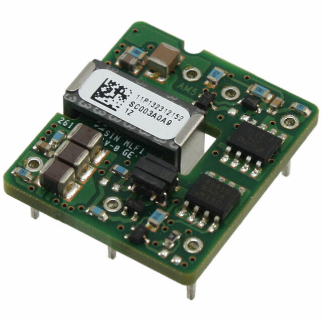
| 产品图片 |
|
| rohs | 符合RoHS无铅 / 符合限制有害物质指令(RoHS)规范要求 |
| 产品系列 | 隔离式DC/DC转换器,Texas Instruments DCR011205PDCR01 |
| mouser_ship_limit | 该产品可能需要其他文档才能发货到中国。 |
| 数据手册 | |
| 产品型号 | DCR011205P |
| 产品 | Isolated |
| 产品目录页面 | |
| 产品种类 | 隔离式DC/DC转换器 |
| 制造商产品页 | http://www.ti.com/general/docs/suppproductinfo.tsp?distId=10&orderablePartNumber=DCR011205P |
| 功率(W)-制造系列 | 1W |
| 功率(W)-最大值 | 1W |
| 包装 | 管件 |
| 商标 | Texas Instruments |
| 大小/尺寸 | 0.90" 长 x 0.28" 宽 x 0.21" 高 (22.9mm x 7.1mm x 5.3mm) |
| 安装类型 | 通孔 |
| 安装风格 | SMD/SMT |
| 封装 | Tube |
| 封装/外壳 | 18-DIP 模块 (10 个接脚) |
| 封装/箱体尺寸 | PDIP-10 |
| 工作温度 | -40°C ~ 85°C |
| 工作温度范围 | - 40 C to + 85 C |
| 工厂包装数量 | 20 |
| 效率 | - |
| 标准包装 | 20 |
| 特性 | 远程开/关,OTP,SCP |
| 电压-输入(最大值) | 13.2V |
| 电压-输入(最小值) | 10.8V |
| 电压-输出1 | 5V |
| 电压-输出2 | - |
| 电压-输出3 | - |
| 电压-隔离 | 1kV(1000V) |
| 电流-输出(最大值) | 200mA |
| 类型 | 隔离模块 |
| 系列 | DCR011205 |
| 输入电压范围 | 10.8 V to 13.2 V |
| 输出功率 | 1 W |
| 输出数 | 1 |
| 输出电压—通道1 | 5.1 V |
| 输出电流—通道1 | 200 mA |
| 输出端数量 | 1 |

.jpg)


- 商务部:美国ITC正式对集成电路等产品启动337调查
- 曝三星4nm工艺存在良率问题 高通将骁龙8 Gen1或转产台积电
- 太阳诱电将投资9.5亿元在常州建新厂生产MLCC 预计2023年完工
- 英特尔发布欧洲新工厂建设计划 深化IDM 2.0 战略
- 台积电先进制程称霸业界 有大客户加持明年业绩稳了
- 达到5530亿美元!SIA预计今年全球半导体销售额将创下新高
- 英特尔拟将自动驾驶子公司Mobileye上市 估值或超500亿美元
- 三星加码芯片和SET,合并消费电子和移动部门,撤换高东真等 CEO
- 三星电子宣布重大人事变动 还合并消费电子和移动部门
- 海关总署:前11个月进口集成电路产品价值2.52万亿元 增长14.8%


PDF Datasheet 数据手册内容提取
Product Sample & Technical Tools & Support & Reference Folder Buy Documents Software Community Design DCR010503,DCR012405,DCR010505 DCR011203,DCR011205,DCR012403 SBVS013D–OCTOBER2001–REVISEDJUNE2016 DCR01 Series, 1-W, 1000-Vrms Isolated, Regulated DC–DC Converter Modules 1 Features 3 Description • 1000-VrmsIsolation(Operational) TheDCR01familyisaseriesofhigh-efficiency,input- 1 isolated, output-regulated DC–DC converters. In • UL1950RecognizedComponent addition to 1 W nominal, galvanically-isolated output • 53W/in3(3.3W/cm3)PowerDensity power capability, this range of DC–DCs offer very low • 10-PinPDIPand12-PinSOPPackages outputnoise,thermalprotection,andhighaccuracy. • Device-to-DeviceSynchronization This combination of features and small size makes • ThermalProtection the DCR01 series of devices suitable for a wide range of applications, and is an easy-to-use solution • 400-kHzSwitching inapplicationsrequiringsignalpathisolation. • 125FITsat55ºC • ±10%InputRange CAUTION • Short-CircuitProtected This product has • 5-V,12-V,and24-VInputs operational isolation and is • 3.3-Vand5-VOutputs intended for signal isolation • HighEfficiency only. It must not be used as a part of a safety 2 Applications isolation circuit requiring reinforced isolation. See • Point-of-UsePowerConversion definitions in Feature • DigitalInterfacePower Description. • GroundLoopElimination • Power-SupplyNoiseReduction DeviceInformation(1) PARTNUMBER PACKAGE BODYSIZE(NOM) PDIP(10) 22.86mm×6.61mm DCR01 SOP(12) 17.90mm×7.50mm (1) For all available packages, see the orderable addendum at theendofthedatasheet. DCR01BlockDiagram +V V S REC +V OUT SYNC Input LDO ERROR Controller Regulator ENABLE -V -V S OUT Copyright © 2016, Texas Instruments Incorporated 1 An IMPORTANT NOTICE at the end of this data sheet addresses availability, warranty, changes, use in safety-critical applications, intellectualpropertymattersandotherimportantdisclaimers.PRODUCTIONDATA.
DCR010503,DCR012405,DCR010505 DCR011203,DCR011205,DCR012403 SBVS013D–OCTOBER2001–REVISEDJUNE2016 www.ti.com Table of Contents 1 Features.................................................................. 1 8.4 DeviceFunctionalModes........................................14 2 Applications........................................................... 1 9 ApplicationandImplementation........................ 15 3 Description............................................................. 1 9.1 ApplicationInformation............................................15 4 RevisionHistory..................................................... 2 9.2 TypicalApplication .................................................17 5 DeviceComparisonTable..................................... 3 10 PowerSupplyRecommendations..................... 18 6 PinConfigurationandFunctions......................... 4 11 Layout................................................................... 18 11.1 LayoutGuidelines.................................................18 7 Specifications......................................................... 5 11.2 LayoutExamples...................................................19 7.1 AbsoluteMaximumRatings......................................5 12 DeviceandDocumentationSupport................. 20 7.2 ESDRatings..............................................................5 7.3 RecommendedOperatingConditions.......................5 12.1 ReceivingNotificationofDocumentationUpdates20 7.4 ThermalInformation..................................................5 12.2 RelatedLinks........................................................20 7.5 ElectricalCharacteristics...........................................6 12.3 CommunityResources..........................................20 7.6 TypicalCharacteristics..............................................7 12.4 Trademarks...........................................................20 12.5 ElectrostaticDischargeCaution............................20 8 DetailedDescription............................................ 11 12.6 Glossary................................................................20 8.1 Overview.................................................................11 13 Mechanical,Packaging,andOrderable 8.2 FunctionalBlockDiagram.......................................11 Information........................................................... 20 8.3 FeatureDescription.................................................11 4 Revision History ChangesfromRevisionC(May2003)toRevisionD Page • AddedDeviceInformationtable,DeviceComparisontable,ESDRatingstable,ThermalInformationtable,Feature Descriptionsection,DeviceFunctionalModes,ApplicationandImplementationsection,PowerSupply Recommendationssection,Layoutsection,DeviceandDocumentationSupportsection,andMechanical, Packaging,andOrderableInformationsection...................................................................................................................... 1 • RemovedPackage/OrderingInformationtable,seePOAattheendofthedatasheet ....................................................... 1 • AddedadditionalgraphstotheTypicalCharacteristicssection ............................................................................................ 7 • AddedIsolationsectiontotheFeatureDescriptionsection ................................................................................................ 11 • AddedatypicalapplicationdesigntotheApplicationInformationsection .......................................................................... 15 2 SubmitDocumentationFeedback Copyright©2001–2016,TexasInstrumentsIncorporated ProductFolderLinks:DCR010503 DCR012405 DCR010505DCR011203 DCR011205 DCR012403
DCR010503,DCR012405,DCR010505 DCR011203,DCR011205,DCR012403 www.ti.com SBVS013D–OCTOBER2001–REVISEDJUNE2016 5 Device Comparison Table atT =25°C,+V =nominal,I =10mA,C =2.2-µFceramic,C =1-µFceramic,C =0.1-µFceramic(unless A S O IN FILTER OUT otherwisenoted) INPUT OUTPUT OUTPUT RIPPLE(2) NOISE(3) SUPPLYCURRENT(mA) DEVICENUMBER(1) VOVLST(AVG)E VOVLOT(AVG)E CU(RmRAE)NT (mVp-p) (mVp-p) IO=0mA IO=10mA IOL=O1A0D0% TYP TYP MAX TYP TYP TYP TYP TYP DCR010503P 5 35 18 28 335 3.3 300 DCR010503U 8 23 24 33 339 5 DCR010505P 6 20 25 40 306 5 200 DCR010505U 9 20 25 40 306 DCR011203P 390 10 54 13 17 173 3.3 DCR011203U 300 8 22 13 17 136 12 DCR011205P 6 45 13 18 125 5 200 DCR011205U 6 21 14 19 123 DCR012403P 390 10 22 17 18 97 3.3 DCR012403U 300 8 22 15 17 75 24 DCR012405P 10 22 15 18 69 5 200 DCR012405U 13 32 15 18 67 (1) Thelastcharacterinthepartnumberdenotesthepackagetype;P=PDIP,U=SOP (2) 20-MHzBandwidth,50%Load (3) 100-MHzBandwidth,50%Load Copyright©2001–2016,TexasInstrumentsIncorporated SubmitDocumentationFeedback 3 ProductFolderLinks:DCR010503 DCR012405 DCR010505DCR011203 DCR011205 DCR012403
DCR010503,DCR012405,DCR010505 DCR011203,DCR011205,DCR012403 SBVS013D–OCTOBER2001–REVISEDJUNE2016 www.ti.com 6 Pin Configuration and Functions NVEPackage 10-PinPDIP DVBPackage TopView 12-PinSOP TopView +VS 1 18 SYNC +VS 1 28 SYNC NC 2 17 -VS +VS 2 27 -VS NC 3 26 -VS DCR01P DCR01U V 7 12 ERROR REC V 12 17 ERROR REC -VOUT 8 11 ENABLE -VOUT 13 16 ENABLE +VOUT 9 10 DNC +VOUT 14 15 DNC PinFunctions PIN I/O DESCRIPTION NAME PDIP SOP ENABLE 11 16 I OutputVoltageEnable ERROR 12 17 O ErrorFlagActiveLow DNC 10 15 — DoNotConnect NC 2 3 — NoConnection SYNC 18 28 I SynchronizationInput –V 8 13 O OutputGround OUT +V 9 14 O VoltageOutput OUT V 7 12 O RectifiedOutput REC –V 17 26,27 I InputGround S +V 1 1,2 I VoltageInput S 4 SubmitDocumentationFeedback Copyright©2001–2016,TexasInstrumentsIncorporated ProductFolderLinks:DCR010503 DCR012405 DCR010505DCR011203 DCR011205 DCR012403
DCR010503,DCR012405,DCR010505 DCR011203,DCR011205,DCR012403 www.ti.com SBVS013D–OCTOBER2001–REVISEDJUNE2016 7 Specifications 7.1 Absolute Maximum Ratings overoperatingfree-airtemperaturerange(unlessotherwisenoted)(1)(2) MIN MAX UNIT 5-Vinputdevices 7 Inputvoltage 12-Vinputdevices 15 V 24-Vinputdevices 29 Surfacetemperatureofdevicebodyorpins Leadtemperature PDIPpackage 270 °C (maximum10s) Reflowsoldertemperature SOPpackage Surfacetemperatureofdevicebodyorpins 260 °C Storagetemperature,T –60 125 °C stg (1) StressesbeyondthoselistedunderAbsoluteMaximumRatingsmaycausepermanentdamagetothedevice.Thesearestressratings only,whichdonotimplyfunctionaloperationofthedeviceattheseoranyotherconditionsbeyondthoseindicatedunderRecommended OperatingConditions.Exposuretoabsolute-maximum-ratedconditionsforextendedperiodsmayaffectdevicereliability. (2) Seethepackageoptionaddendumattheendofthedatasheetforadditionalpackageinformation. 7.2 ESD Ratings VALUE UNIT Human-bodymodel(HBM),perANSI/ESDA/JEDECJS-001(1) ±1000 V Electrostaticdischarge V (ESD) Charged-devicemodel(CDM),perJEDECspecificationJESD22-C101(2) ±250 (1) JEDECdocumentJEP155statesthat500-VHBMallowssafemanufacturingwithastandardESDcontrolprocess. (2) JEDECdocumentJEP157statesthat250-VCDMallowssafemanufacturingwithastandardESDcontrolprocess. 7.3 Recommended Operating Conditions overoperatingfree-airtemperaturerange(unlessotherwisenoted) MIN NOM MAX UNIT 5-Vinputdevices 4.5 5 5.5 Inputvoltage 12-Vinputdevices 10.8 12 13.2 V 24-Vinputdevices 21.6 24 26.4 Operatingtemperature –40 85 °C 7.4 Thermal Information DCR01 THERMALMETRIC(1) NVE(PDIP) DVB(SOP) UNIT 10PINS 12PINS R Junction-to-ambientthermalresistance 60 60 °C/W θJA R Junction-to-case(top)thermalresistance 26 26 °C/W θJC(top) R Junction-to-boardthermalresistance 24 24 °C/W θJB ψ Junction-to-topcharacterizationparameter 7 7 °C/W JT ψ Junction-to-boardcharacterizationparameter 24 24 °C/W JB (1) Formoreinformationabouttraditionalandnewthermalmetrics,seetheSemiconductorandICPackageThermalMetricsapplication report. Copyright©2001–2016,TexasInstrumentsIncorporated SubmitDocumentationFeedback 5 ProductFolderLinks:DCR010503 DCR012405 DCR010505DCR011203 DCR011205 DCR012403
DCR010503,DCR012405,DCR010505 DCR011203,DCR011205,DCR012403 SBVS013D–OCTOBER2001–REVISEDJUNE2016 www.ti.com 7.5 Electrical Characteristics atT =25°C,+V =nominal,I =10mA,C =2.2-µFceramic,C =1-µFceramic,C =0.1-µFceramic(unless A S O IN FILTER OUT otherwisenoted) PARAMETER TESTCONDITIONS MIN TYP MAX UNIT OUTPUT DCR01xx03 3.3 Nominaloutputvoltage(+V ) V OUT DCR01xx05 5 Setpointaccuracy 0.5% 2% Outputshort-circuitprotected Duration Infinite Lineregulation 1 mV/V Overlineandload I =10mAtoFullLoad,Over+V range 1% 2.5% O S Temperaturevariation –40°C≤T ≤+85°C 1% A INPUT DCR0105xx 5 Nominalinputvoltage(+V ) DCR0112xx 12 V S DCR0124xx 24 Voltagerange –10% 10% Reflectedripplecurrent 20-MHzBandwidth,I =100%Load 8 mAp-p O ISOLATION Voltage 1 kVrms 1-sFlashTest dV/dt 500 V/s Isolation LeakageCurrent 30 nA Continuousworking DC 60 VDC voltageacrossisolation barrier AC 42.5 VAC Barriercapacitance 25 pF OUTPUTENABLECONTROL Logichighinputvoltage 2 V V REC Logichighinputcurrent 2<V <V 100 nA ENABLE REC Logiclowinputvoltage –0.2 0.5 V Logiclowinputcurrent 0<V <0.5 100 nA ENABLE All3.3-VOutputs 3.3 Rectifiedoutput,V V REC All5-VOutputs 5 ERRORFLAG Logichighopen-collectorleakage V =5V 10 µA ERROR Logiclowoutputvoltage Sinking2mA 0.4 V THERMALSHUTDOWN TemperatureActivated 150 Junctiontemperature °C TemperatureDeactivated 130 SYNCHRONIZATIONPIN MaxexternalcapacitanceonSYNCpin 3 pF Internaloscillatorfrequency 720 800 880 kHz Externalsynchronizationfrequency 720 880 kHz Externalsynchronizationsignalhigh 2.5 3 V Externalsynchronizationsignallow 0 0.4 V TEMPERATURERANGE Operating –40 85 °C 6 SubmitDocumentationFeedback Copyright©2001–2016,TexasInstrumentsIncorporated ProductFolderLinks:DCR010503 DCR012405 DCR010505DCR011203 DCR011205 DCR012403
DCR010503,DCR012405,DCR010505 DCR011203,DCR011205,DCR012403 www.ti.com SBVS013D–OCTOBER2001–REVISEDJUNE2016 7.6 Typical Characteristics atT =25°C,+V =nominal,I =10mA,C =2.2µF,C =1µF,C =0.1µF,(unlessotherwisenoted) A S O IN FILTER OUT 70 80 85°C +85°C 60 70 +25°C 60 50 %) –40°C %) 50 Efficiency ( 4300 25°C Effeciency ( 4300 –40°C 20 20 10 10 0 0 0 10 20 30 40 50 60 70 80 90 100 0 10 20 30 40 50 60 70 80 90 100 Load (%) Load (%) DCR010503P, DCR010503U DCR010505P, DCR010505U DCR011205P, DCR011205U DCR011205P, DCR011205U Figure1.EfficiencyvsLoad Figure2.EfficiencyvsLoad 60 70 60 50 50 %) 40 %) ncy ( 30 ncy ( 40 Efficie 20 Efficie 30 20 10 10 0 0 0 10 20 30 40 50 60 70 80 90 100 0 10 20 30 40 50 60 70 80 90 100 Load% Load (%) DCR012403P DCR012403U DCR010505U DCR011205U Figure3.EfficiencyvsLoad Figure4.EfficiencyvsLoad 70 18 16 60 14 %) 50 mVp-p) 12 y ( 40 e ( 10 c g n a Efficie 30 e Volt 86 20 ppl Ri 4 10 2 0 0 0 10 20 30 40 50 60 70 80 90 100 0 20 40 60 80 100 Load (%) Load (%) DCR012405P DCR012405U AlldevicesexceptforDCR011203P&DCR012403P 20-MHzBandwidth Figure5.EfficiencyvsLoad Figure6.OutputVoltageRipple Copyright©2001–2016,TexasInstrumentsIncorporated SubmitDocumentationFeedback 7 ProductFolderLinks:DCR010503 DCR012405 DCR010505DCR011203 DCR011205 DCR012403
DCR010503,DCR012405,DCR010505 DCR011203,DCR011205,DCR012403 SBVS013D–OCTOBER2001–REVISEDJUNE2016 www.ti.com Typical Characteristics (continued) atT =25°C,+V =nominal,I =10mA,C =2.2µF,C =1µF,C =0.1µF,(unlessotherwisenoted) A S O IN FILTER OUT 30.0 80 70 25.0 p) 60 p- mV 20.0 p) 50 age ( 15.0 mVp- 40 ple Volt 10.0 Noise ( 30 p Ri 20 5.0 10 0 0 0 20 40 60 80 100 0 20 40 60 80 100 Load (%) Load (%) DCR011203P 20-MHzBandwidth All5-VInputDevices 100-MHzBandwidth DCR012403P Figure7.OutputVoltageRipple Figure8.OutputVoltageNoise 120.0 60.0 100.0 50.0 Vp-p) 80.0 Vp-p) 40.0 Noise (m 6400..00 Noise (m 3200..00 20.0 10.0 0 0 0 20 40 60 80 100 0% 20% 40% 60% 80% 100% Load (%) Load% DCR011203P 100-MHzBandwidth DCR011205P 100-MHzBandwidth Figure9.OutputVoltageNoise Figure10.OutputVoltageNoise All5-VOutputDevices All3.3-VoutputdevicesexceptDCR010503P Figure11.5-VOutputLoadRegulation Figure12.3.3-VOutputLoadRegulation 8 SubmitDocumentationFeedback Copyright©2001–2016,TexasInstrumentsIncorporated ProductFolderLinks:DCR010503 DCR012405 DCR010505DCR011203 DCR011205 DCR012403
DCR010503,DCR012405,DCR010505 DCR011203,DCR011205,DCR012403 www.ti.com SBVS013D–OCTOBER2001–REVISEDJUNE2016 Typical Characteristics (continued) atT =25°C,+V =nominal,I =10mA,C =2.2µF,C =1µF,C =0.1µF,(unlessotherwisenoted) A S O IN FILTER OUT 3.305 85°C 3.3 3.295 3.29 V) v (UT 3.285 A/di VO 3.28 25°C 0m 2 3.275 3.27 –40°C 3.265 0 10 20 30 40 50 60 70 80 90 100 Load (%) 500ns/div DCR010503P 20-MHzBandwidth Figure13.3.3-VOutputLoadRegulation Figure14.InputCurrentReflectedRipple A/div V/div m m 40 5 500ns/div 200ns/div 100-MHzBandwidth 20-MHzBandwidth Figure15.InputCurrentReflectedRipple Figure16.DCR010505POutputVoltageRipple at100%Load V/div V/div m m 20 5 200ns/div 200ns/div 100-MHzBandwidth 20-MHzBandwidth Figure17.DCR010505POutputVoltageNoise Figure18.DCR010503POutputVoltageRipple at100%Load at100%Load Copyright©2001–2016,TexasInstrumentsIncorporated SubmitDocumentationFeedback 9 ProductFolderLinks:DCR010503 DCR012405 DCR010505DCR011203 DCR011205 DCR012403
DCR010503,DCR012405,DCR010505 DCR011203,DCR011205,DCR012403 SBVS013D–OCTOBER2001–REVISEDJUNE2016 www.ti.com Typical Characteristics (continued) atT =25°C,+V =nominal,I =10mA,C =2.2µF,C =1µF,C =0.1µF,(unlessotherwisenoted) A S O IN FILTER OUT Load Current Load Current g n giA anm h5 C2 3 div 0mAto V/ 3 m 0 2 Output Voltage Output Voltage v di V/ m 0 0 2 200ns/div 100-MHzBandwidth 10µs/div Figure19.DCR010503POutputVoltageNoise Figure20.DCR010503PLoadTransientResponse at100%Load 150mAChangingto 300mA Load Current 20mAChangingto 200mA Load Current v mV/di Output Voltage V/div Output Voltage 0 m 0 0 2 0 2 10µs/div 10µs/div Figure21.DCR010503PLoadTransientResponse Figure22.DCR010505PLoadTransientResponse g Load Current n ngiA am Ch00 mAo 2 0t 0 1 div Output Voltage V/ m 0 0 2 10µs/div Figure23.DCR010505PLoadTransientResponse 10 SubmitDocumentationFeedback Copyright©2001–2016,TexasInstrumentsIncorporated ProductFolderLinks:DCR010503 DCR012405 DCR010505DCR011203 DCR011205 DCR012403
DCR010503,DCR012405,DCR010505 DCR011203,DCR011205,DCR012403 www.ti.com SBVS013D–OCTOBER2001–REVISEDJUNE2016 8 Detailed Description 8.1 Overview The DCR01 series of power modules offer isolation from a regulated power supply operating from a choice of input voltages. The DCR01s provide a regulated 3.3-V or 5-V output voltage at a nominal output power of 1 W or above. The DCR01 devices include a low dropout linear regulator internal to the device to achieve a well- regulated output voltage. The DCR01 devices are specified for operational isolation only. The circuit design uses anadvancedBiCMOS/DMOSprocess. 8.2 Functional Block Diagram SYNC +V V S REC +V OUT Oscillator Divide-by-2 800 kHz Reset LDO Power ERROR Regulator Stage Watchdog Startup ENABLE PSU Thermal Input Shutdown Controller -V -V S OUT Copyright © 2016, Texas Instruments Incorporated 8.3 Feature Description 8.3.1 Isolation UnderwritersLaboratories,UL™,definesseveralclassesofisolationthatareusedinmodernpowersupplies. Safety extra low voltage (SELV) is defined by UL (UL1950 E199929) as a secondary circuit which is so designated and protected that under normal and single fault conditions the voltage between any two accessible parts, or between an accessible part and the equipment earthing terminal for operational isolation does not exceedsteadystate42.4V or60V peak. RMS DC 8.3.1.1 OperationorFunctionalIsolation The type of isolation used in the DCR01 products is referred to as operational or functional isolation. Insulated wire used in the construction of the transformer acts as the primary isolation barrier. A high-potential (hipot), one- second duration test (dielectric voltage, withstand test) is a production test used to verify that the isolation barrier isfunctioning.Productswithoperationalisolationmustneverbeusedasanelementinasafety-isolationsystem. 8.3.1.2 BasicorEnhancedIsolation Basic or enhanced isolation is defined by specified creepage and clearance limits between the primary and secondarycircuitsofthepowersupply.Basicisolationistheuseofanisolationbarrierinadditiontotheinsulated wire in the construction of the transformer. Input and output circuits must also be physically separated by specifieddistances. Copyright©2001–2016,TexasInstrumentsIncorporated SubmitDocumentationFeedback 11 ProductFolderLinks:DCR010503 DCR012405 DCR010505DCR011203 DCR011205 DCR012403
DCR010503,DCR012405,DCR010505 DCR011203,DCR011205,DCR012403 SBVS013D–OCTOBER2001–REVISEDJUNE2016 www.ti.com Feature Description (continued) NOTE TheDCR01productsDONOTprovidebasicorenhancedisolation. 8.3.1.3 WorkingVoltage For a device with operational isolation, the continuous working voltage that can be applied across the device in normaloperationmustbelessthan42.4V or60V ,(SELVlimits). RMS DC WARNING Do not use the device as an element of a safety isolation system if SELV is exceeded. Ifthedeviceisexpectedtofunctioncorrectlywithmorethan42.4V or60V appliedcontinuouslyacrossthe RMS DC isolation barrier, then the circuitry on both sides of the barrier must be regarded as operating at an unsafe voltage, and further isolation or insulation systems must form a barrier between these circuits and any user- accessiblecircuitryaccordingtosafetystandardrequirements. 8.3.1.4 IsolationVoltageRating The terms Hipot test,flash-tested,withstand voltage,proof voltage, dielectric withstand voltage, and isolation test voltage are all terms that relate to the same thing; a test voltage applied for a specified time across a component designed to provide electrical isolation to verify the integrity of that isolation. TI’s DCR01 series of DC-DC convertersareall100%productiontestedat1kV foronesecond. AC 8.3.1.5 RepeatedHigh-VoltageIsolationTesting Repeatedhigh-voltageisolationtestingofabarriercomponentcandegradetheisolationcapability,dependingon materials, construction, and environment. The DCV01 series of DC–DC converters have toroidal, enameled, wire isolation transformers with no additional insulation between the primary and secondary windings. While a device can be expected to withstand several times the stated test voltage, the isolation capability depends on the wire insulation. Any material, including this enamel (typically polyurethane), is susceptible to eventual chemical degradation when subject to very-high applied voltages. Therefore, strictly limit the number of high-voltage tests and repeated high-voltage isolation testing. However, if it is absolutely required, reduce the voltage by 20% from specifiedtestvoltagewithadurationlimitofonesecondpertest. 8.3.2 PowerStage The DCR01 series of devices use a push-pull, center-tapped topology. The DCV01 devices switch at 400 kHz (divide-by-2froman800-kHzoscillator). 8.3.3 Rectification The transformer’s output is full wave rectified and filtered by the external 1-μF ceramic capacitor connected to V . REC 8.3.4 Regulator The internal low dropout linear regulator provides a well-regulated output voltage throughout the operating range ofthedevice. 8.3.5 OscillatorandWatchdog The onboard, 800-kHz oscillator generates the switching frequency through a divide-by-2 circuit. The oscillator can be synchronized to other DCR01 device circuits or an external source, and is used to minimize system noise. 12 SubmitDocumentationFeedback Copyright©2001–2016,TexasInstrumentsIncorporated ProductFolderLinks:DCR010503 DCR012405 DCR010505DCR011203 DCR011205 DCR012403
DCR010503,DCR012405,DCR010505 DCR011203,DCR011205,DCR012403 www.ti.com SBVS013D–OCTOBER2001–REVISEDJUNE2016 Feature Description (continued) A watchdog circuit monitors the operation of the oscillator circuit. The oscillator can be disabled by pulling the SYNC pin low. When the SYNC pin goes low, the output pins transition into tri-state mode, which occurs within 2μs. 8.3.6 ERROR Flag The DCR01 has an ERROR pin which provides a power good flag, as long as the internal regulator is in regulation. If the ERROR output is required, place a 10-kΩ resistor between the ERROR pin and the output voltage. 8.3.7 Synchronization When more than one DC–DC converter is switching in an application, beat frequencies and other electrical interference can be generated. This interference occurs because of the small variations in switching frequencies betweentheDC–DCconverters. The DCR01 series of devices overcome this interference by allowing devices to be synchronized to one another. Synchronize up to eight devices by connecting the SYNC pins of each device, taking care to minimize the capacitance of tracking. Stray capacitance (greater than 3 pF) reduces the switching frequency, or can sometimesstoptheoscillatorcircuit.ThemaximumrecommendedvoltageappliedtotheSYNCpinis3V. For an application that uses more than eight synchronized devices use an external device to drive the SYNC pins. The application report External Synchronization of the DCP01/02 Series of DC/DC Converters describes thisconfiguration. NOTE During the start-up period, all synchronized devices draw maximum current from the input simultaneously. If the input voltage falls below approximately 4 V, the devices may not start up. A ceramic capacitor should be connected close to each device's input pin. Use a 2.2-μF capacitor for 5-V input devices, and a 0.47-μF capacitor for the 12-V and 24-V devices. 8.3.8 Construction The basic construction of the DCR01 series of devices is the same as standard integrated circuits. The molded package contains no substrate. The DCV01 series of devices are constructed using an IC, low dropout linear regulator, rectifier diodes, and a wound magnetic toroid on a leadframe. Because the package contains no solder, the devices do not require any special printed-circuit board (PCB) assembly processing. This architecture resultsinanisolatedDC–DCconverterwithinherentlyhighreliability. 8.3.9 ThermalConsiderations Due to the high power density of this device, it is advisable to provide ground planes on the input and output rails.Theoutputregulatorismountedonacopperleadframe,andagroundplaneservesasanefficientheatsink. 8.3.10 Decoupling – RippleReduction DuetotheverylowforwardresistanceoftheDMOSswitchingtransistors,highcurrentdemandsareplacedupon the input supply for a short time. By using a good quality low Equivalent Series Resistance (ESR) capacitor of 2.2 μF (minimum) for the 5-V input devices and a 0.47-μF capacitor for the 12-V and 24-V devices, placed close totheICsupplyinputpins,theeffectsonthepowersupplycanbeminimized. The high switching frequency of 400 kHz allows relatively small values of capacitors to be used for filtering the rectified output voltage. A good-quality, low-ESR, 1-μF ceramic capacitor placed close to the VREC pin and output ground is required and reduces the ripple. The output at VREC is full wave rectified and produces a ripple of800kHz. TI recommends that a 0.1-μF, low-ESR, ceramic capacitor is connected close to the output pin and ground to reduce noise on the output. The capacitor values listed are minimum values. If lower ripple is required, the filter capacitorshouldbeincreasedinvalueto2.2 μF. Copyright©2001–2016,TexasInstrumentsIncorporated SubmitDocumentationFeedback 13 ProductFolderLinks:DCR010503 DCR012405 DCR010505DCR011203 DCR011205 DCR012403
DCR010503,DCR012405,DCR010505 DCR011203,DCR011205,DCR012403 SBVS013D–OCTOBER2001–REVISEDJUNE2016 www.ti.com Feature Description (continued) As with all switching power supplies, the best performance is obtained with low ESR,ceramic capacitors connected close to the device pins. If low ESR, ceramic capacitors are not used, the ESR generates a voltage drop when the capacitor is supplying the load power. Often a larger capacitor is chosen for this purpose, when a lowESR,smallercapacitorwouldperformaswell. NOTE TI does not recommend that the DCR01 be fitted using an IC socket, as this degrades performance. 8.4 Device Functional Modes 8.4.1 DeviceDisableandEnable Each of the DCR01 series devices can be disabled or enabled by driving the SYNC pin using an open-drain CMOS gate. If the SYNC pin is pulled low, the DCR01 becomes disabled. The disable time depends upon the external loading. The internal disable function is implemented in 2 μs. Removal of the pulldown causes the DCR01tobeenabled. Capacitive loading on the SYNC pin must be minimized (≤ 3 pF) to prevent a reduction in the oscillator frequency. The application report External Synchronization of the DCP01/02 Series of DC/DC Converters describes disable and enable control circuitry. This document contains information on how to null the effects of additional capacitance on the SYNC pin. The oscillator’s frequency can be measured at V , as this is the REC fundamentalfrequencyoftheripplecomponent. 8.4.2 RegulatedOutputDisableandEnable The regulated output of the DCR01 can be disabled by pulling the ENABLE pin LOW. Disabling the output voltage this way still produces a voltage on the V pin. When using the ENABLE control, TI recommends REC placing a 10-kΩ resistor between the V and ENABLE pins. The ENABLE pin only controls the internal linear REC regulator. If disabling the regulated output is not required, pull the ENABLE pin HIGH by shorting it directly to the V pin. REC Thisenablestheregulatedoutputvoltage,thusallowingtheoutputtobecontrolledfromtheisolatedside. 14 SubmitDocumentationFeedback Copyright©2001–2016,TexasInstrumentsIncorporated ProductFolderLinks:DCR010503 DCR012405 DCR010505DCR011203 DCR011205 DCR012403
DCR010503,DCR012405,DCR010505 DCR011203,DCR011205,DCR012403 www.ti.com SBVS013D–OCTOBER2001–REVISEDJUNE2016 9 Application and Implementation NOTE Information in the following applications sections is not part of the TI component specification, and TI does not warrant its accuracy or completeness. TI’s customers are responsible for determining suitability of components for their purposes. Customers should validateandtesttheirdesignimplementationtoconfirmsystemfunctionality. 9.1 Application Information 9.1.1 DCR01SingleVoltageOutput The DCR01 can be used to provide a single voltage output by connecting it as shown in Figure 24. The ERROR output signal will be pulled up to the value of V . The value of R will depend on the loading on the ERROR OUT ERR line;however,thetotalloadonthe ERROR linemustnotexceedthevaluegiveninElectricalCharacteristics. The output may be permanently enabled by connecting the ENABLE pin to the V pin. The DCR01 may be REC enabledremotelybyconnectingtheENABLEpintoV throughapullupresistor(R );thevalueofthisresistor REC EN is not critical for the DCR01 as only a small current flows. The switch SW1 can be used to pull the ENABLE pin LOW, thus disabling the output. The switching devices can be a bipolar transistor, FET, or a mechanical device; themainloadthatitseesisR . EN SYNC +VOUT RERR +VOUT 10 k(cid:13) VIN +VS ERROR ERROR VREC COUT CIN(1) DCR01 ENABLE REN 0.1 µF 10k(cid:13) CFILTER SW1 1 µF –VS –VOUT –VOUT (1)C =2.2μFfor5-Vinputdevicesand0.47μFfor12-Vand24-Vinputdevices.LowESR,ceramiccapacitorsare IN required. Figure24. DCR01SingleOutputVoltage Copyright©2001–2016,TexasInstrumentsIncorporated SubmitDocumentationFeedback 15 ProductFolderLinks:DCR010503 DCR012405 DCR010505DCR011203 DCR011205 DCR012403
DCR010503,DCR012405,DCR010505 DCR011203,DCR011205,DCR012403 SBVS013D–OCTOBER2001–REVISEDJUNE2016 www.ti.com Application Information (continued) 9.1.2 GeneratingTwoPositiveOutputVoltages Two DCR01s can be used to create output voltages of +3.3 V and +5 V, as shown in Figure 25. The two DCR01s are connected in self-synchronization, thus locking the oscillators of both devices to a single frequency. The ERROR and ENABLE facilities may be used in a similar configuration for a single DCR01. The filter capacitors connected to the V pins (C ) must be kept separate from each other and connected in close REC FILTER proximitytotheirrespectiveDCR01. VIN +VS +VOUT RERR +VOUT1 10 k(cid:13) CIN(1) ERVRROERC COUT ERROR1 DCR01 0.1 µF –VS ENABLE C1 FµILFTER SYNC –VOUT -VOUT SYNC +VOUT RERR +VOUT2 10 k(cid:13) VIN +VS ERROR ERROR2 VREC COUT CIN(1) DCR01 ENABLE CFILTER 0.1 µF 1 µF –VS –VOUT (1)C =2.2μFfor5-Vinputdevicesand0.47μFfor12-Vand24-Vinputdevices.LowESR,ceramiccapacitorsare IN required. Figure25. TwoPositiveVoltagesfromSelf-SynchronizedDCR01s 9.1.3 GenerationofDualPolarityVoltagesfromTwoSelf-SynchronizedDCR01s TwoDCR01scanbeconfiguredtoproduceadualpolaritysupply(thatis,±5V);thecircuitmustbeconnectedas showninFigure26. Itmustbeobservedthatbothdevicesareproducingapositiveregulatedoutput;thereforetheERROR,ENABLE, and VREC are all relative to that particular device's –V pin and must not be directly connected together, or in OUT thecaseofthenegativeoutputdevice,connectedtothecommon0-Voutput. VIN +VS +VOUT VPOS O/P CIN(1) ERVRROERC COUT DCR01 0.1 µF –VS ENABLE C1 FµILFTER SYNC –VOUT 0V SYNC +VOUT VIN +VS ERROR VREC COUT CIN(1) DCR01 ENABLE CFILTER 0.1 µF 1 µF –VS –VOUT VNEG O/P (1)C =2.2μFfor5-Vinputdevicesand0.47μFfor12-Vand24-Vinputdevices.LowESR,ceramiccapacitorsare IN required. Figure26. DualPolarityVoltageGeneration 16 SubmitDocumentationFeedback Copyright©2001–2016,TexasInstrumentsIncorporated ProductFolderLinks:DCR010503 DCR012405 DCR010505DCR011203 DCR011205 DCR012403
DCR010503,DCR012405,DCR010505 DCR011203,DCR011205,DCR012403 www.ti.com SBVS013D–OCTOBER2001–REVISEDJUNE2016 9.2 Typical Application DCR010505 +VOUT = 5V SYNC +VOUT VIN = 5V 1R0E kR(cid:13)R +VS ERROR CIN VREC C0.O1U µTF 2.2 µF ENABLE CFILTER –VS 1.0 µF –VOUT –VOUT Copyright © 2016, Texas Instruments Incorporated Figure27. DCR01TypicalSchematic 9.2.1 DesignRequirements Forthisdesignexample,usetheparameterslistedinTable1andfollowthedesignprocedure. Table1.DesignExampleParameters DESIGNPARAMETER VALUE InputVoltageV 5Vtypical IN OutputVoltageV 5Vregulated OUT OutputCurrentRating 200mA Isolation 1000-Voperational 9.2.2 DetailedDesignProcedure 9.2.2.1 InputCapacitor Forthisdesign,a2.2-μF,ceramiccapacitorisrequiredfortheinputdecouplingcapacitor. 9.2.2.2 OutputCapacitor Forthisdesign,a0.1-μF,ceramiccapacitorisrequiredforbetween+V and –V . OUT OUT 9.2.2.3 FilterCapacitor A high-quality, low-ESR, 1-μF, ceramic capacitor placed close to the VREC pin and output ground is required to reduceoutputvoltageripple. 9.2.2.4 ERROR Flag Place a 10-kΩ resistor between the ERROR pin and the output voltage to provide a power good signal when the internalregulatorisinregulation. Copyright©2001–2016,TexasInstrumentsIncorporated SubmitDocumentationFeedback 17 ProductFolderLinks:DCR010503 DCR012405 DCR010505DCR011203 DCR011205 DCR012403
DCR010503,DCR012405,DCR010505 DCR011203,DCR011205,DCR012403 SBVS013D–OCTOBER2001–REVISEDJUNE2016 www.ti.com 9.2.3 ApplicationCurves 80 +85°C 70 +25°C 60 %) 50 y ( c n 40 cie –40°C Effe 30 20 10 0 0 10 20 30 40 50 60 70 80 90 100 Load (%) Figure28.DCR010505Efficiency Figure29.DCR010505LoadRegulation 10 Power Supply Recommendations The DCR01 is a switching power supply, and as such can place high peak current demands on the input supply. To avoid the supply falling momentarily during the fast switching pulses, ground and power planes must be used to connect the power to the input of DCR01. If this connection is not possible, then the supplies must be connectedinastarformationwiththetracesmadeaswideaspossible. 11 Layout 11.1 Layout Guidelines CarefullyconsiderthelayoutofthePCBinorderforthebestresultstobeobtained. Input and output power and ground planes provide a low-impedance path for the input and output power. For the output,thepositiveandnegativevoltageoutputsconductthroughwidetracestominimizelosses. A good-quality, low-ESR, ceramic capacitor placed as close as practical across the input reduces reflected ripple andensureasmoothstart-up. A good-quality, low-ESR, ceramic capacitor placed as close as practical across the rectifier output terminal and outputgroundgivesthebestrippleandnoiseperformance. Thelocationofthedecouplingcapacitorsincloseproximitytotheirrespectivepinsensureslowlossesduetothe effects of stray inductance, thus improving the ripple performance. This location is of particular importance to the input decoupling capacitor, because this capacitor supplies the transient current associated with the fast switchingwaveformsofthepowerdrivecircuits. If the SYNC pin is being used, the tracking between device SYNC pins must be short to avoid stray capacitance. Never connect a capacitor to the SYNC pin. If the SYNC pin is not being used it is advisable to place a guard ring (connected to input ground) around this pin to avoid any noise pick-up. Ensure that no other trace is in close proximity to this trace SYNC trace to decrease the stray capacitance on this pin. The stray capacitance affects theperformanceoftheoscillator. Figure 30 shows a schematic for a single DCR01, SOP package device. Figure 31 and Figure 32 show a typical layoutfortheSOPpackageDCR01device.Thelayoutshowsproperplacementofcapacitorsandpowerplanes. 18 SubmitDocumentationFeedback Copyright©2001–2016,TexasInstrumentsIncorporated ProductFolderLinks:DCR010503 DCR012405 DCR010505DCR011203 DCR011205 DCR012403
DCR010503,DCR012405,DCR010505 DCR011203,DCR011205,DCR012403 www.ti.com SBVS013D–OCTOBER2001–REVISEDJUNE2016 11.2 Layout Examples DCR01U U1 1 +VS +VS 2 +VS C1 SYNC 28 -VS 26 –VS 27 –VS ERROR 17 VREC 12 VREC C2 ENABLE 16 -VOUT 13 –VOUT C3 +VOUT 14 +VOUT Figure30. DCR01PCBSchematic,UPackage U1 SYNC SYNC +V +V S S -VS C1 -VS V C2 V REC REC ERROR ERROR ENABLE ENABLE -V -V OUT OUT +VOUT C3 +VOUT Figure31.PCBLayoutExample, Figure32.PCBLayoutExample, Component-SideView Non-Component-SideView Copyright©2001–2016,TexasInstrumentsIncorporated SubmitDocumentationFeedback 19 ProductFolderLinks:DCR010503 DCR012405 DCR010505DCR011203 DCR011205 DCR012403
DCR010503,DCR012405,DCR010505 DCR011203,DCR011205,DCR012403 SBVS013D–OCTOBER2001–REVISEDJUNE2016 www.ti.com 12 Device and Documentation Support 12.1 Receiving Notification of Documentation Updates To receive notification of documentation updates, navigate to the device product folder on ti.com. In the upper right corner, click on Alert me to register and receive a weekly digest of any product information that has changed.Forchangedetails,reviewtherevisionhistoryincludedinanyreviseddocument. 12.2 Related Links The table below lists quick access links. Categories include technical documents, support and community resources,toolsandsoftware,andquickaccesstosampleorbuy. Table2.RelatedLinks TECHNICAL TOOLS& SUPPORT& PARTS PRODUCTFOLDER SAMPLE&BUY DOCUMENTS SOFTWARE COMMUNITY DCR010503 Clickhere Clickhere Clickhere Clickhere Clickhere DCR012405 Clickhere Clickhere Clickhere Clickhere Clickhere DCR010505 Clickhere Clickhere Clickhere Clickhere Clickhere DCR011203 Clickhere Clickhere Clickhere Clickhere Clickhere DCR011205 Clickhere Clickhere Clickhere Clickhere Clickhere DCR012403 Clickhere Clickhere Clickhere Clickhere Clickhere 12.3 Community Resources The following links connect to TI community resources. Linked contents are provided "AS IS" by the respective contributors. They do not constitute TI specifications and do not necessarily reflect TI's views; see TI's Terms of Use. TIE2E™OnlineCommunity TI'sEngineer-to-Engineer(E2E)Community.Createdtofostercollaboration amongengineers.Ate2e.ti.com,youcanaskquestions,shareknowledge,exploreideasandhelp solveproblemswithfellowengineers. DesignSupport TI'sDesignSupport QuicklyfindhelpfulE2Eforumsalongwithdesignsupporttoolsand contactinformationfortechnicalsupport. 12.4 Trademarks E2EisatrademarkofTexasInstruments. UnderwritersLaboratories,ULaretrademarksofULLLC. Allothertrademarksarethepropertyoftheirrespectiveowners. 12.5 Electrostatic Discharge Caution This integrated circuit can be damaged by ESD. Texas Instruments recommends that all integrated circuits be handled with appropriateprecautions.Failuretoobserveproperhandlingandinstallationprocedurescancausedamage. ESDdamagecanrangefromsubtleperformancedegradationtocompletedevicefailure.Precisionintegratedcircuitsmaybemore susceptibletodamagebecauseverysmallparametricchangescouldcausethedevicenottomeetitspublishedspecifications. 12.6 Glossary SLYZ022—TIGlossary. Thisglossarylistsandexplainsterms,acronyms,anddefinitions. 13 Mechanical, Packaging, and Orderable Information The following pages include mechanical, packaging, and orderable information. This information is the most current data available for the designated devices. This data is subject to change without notice and revision of thisdocument.Forbrowser-basedversionsofthisdatasheet,refertotheleft-handnavigation. 20 SubmitDocumentationFeedback Copyright©2001–2016,TexasInstrumentsIncorporated ProductFolderLinks:DCR010503 DCR012405 DCR010505DCR011203 DCR011205 DCR012403
PACKAGE OPTION ADDENDUM www.ti.com 12-Aug-2017 PACKAGING INFORMATION Orderable Device Status Package Type Package Pins Package Eco Plan Lead/Ball Finish MSL Peak Temp Op Temp (°C) Device Marking Samples (1) Drawing Qty (2) (6) (3) (4/5) DCR010503P ACTIVE PDIP NVE 10 20 Pb-Free CU NIPDAU N / A for Pkg Type -40 to 85 DCR010503P (RoHS) DCR010503U ACTIVE SOP DVB 12 28 Pb-Free CU NIPDAU Level-3-260C-168 HR -40 to 85 DCR010503U (RoHS) DCR010503U/1K ACTIVE SOP DVB 12 1000 Pb-Free CU NIPDAU Level-3-260C-168 HR -40 to 85 DCR010503U (RoHS) DCR010503UE4 ACTIVE SOP DVB 12 28 Pb-Free CU NIPDAU Level-3-260C-168 HR -40 to 85 DCR010503U (RoHS) DCR010505P ACTIVE PDIP NVE 10 20 Pb-Free CU NIPDAU N / A for Pkg Type -40 to 85 DCR010505P (RoHS) DCR010505U ACTIVE SOP DVB 12 28 Pb-Free CU NIPDAU Level-3-260C-168 HR -40 to 85 DCR010505U (RoHS) DCR010505U/1K ACTIVE SOP DVB 12 1000 Pb-Free CU NIPDAU Level-3-260C-168 HR -40 to 85 DCR010505U (RoHS) DCR010505U/1KE4 ACTIVE SOP DVB 12 1000 Pb-Free CU NIPDAU Level-3-260C-168 HR -40 to 85 DCR010505U (RoHS) DCR010505UE4 ACTIVE SOP DVB 12 28 Pb-Free CU NIPDAU Level-3-260C-168 HR -40 to 85 DCR010505U (RoHS) DCR011203P ACTIVE PDIP NVE 10 20 TBD CU NIPDAU N / A for Pkg Type -40 to 85 DCR011203P DCR011203U ACTIVE SOP DVB 12 28 Pb-Free CU NIPDAU Level-3-260C-168 HR -40 to 85 DCR011203U (RoHS) DCR011203U/1K ACTIVE SOP DVB 12 1000 Pb-Free CU NIPDAU Level-3-260C-168 HR -40 to 85 DCR011203U (RoHS) DCR011203UE4 ACTIVE SOP DVB 12 28 Pb-Free CU NIPDAU Level-3-260C-168 HR -40 to 85 DCR011203U (RoHS) DCR011205P ACTIVE PDIP NVE 10 20 Pb-Free CU NIPDAU N / A for Pkg Type -40 to 85 DCR011205P (RoHS) DCR011205U ACTIVE SOP DVB 12 28 Pb-Free CU NIPDAU Level-3-260C-168 HR -40 to 85 DCR011205U (RoHS) DCR011205U/1K ACTIVE SOP DVB 12 1000 Pb-Free CU NIPDAU Level-3-260C-168 HR -40 to 85 DCR011205U (RoHS) DCR011205UE4 ACTIVE SOP DVB 12 28 Pb-Free CU NIPDAU Level-3-260C-168 HR -40 to 85 DCR011205U (RoHS) Addendum-Page 1
PACKAGE OPTION ADDENDUM www.ti.com 12-Aug-2017 Orderable Device Status Package Type Package Pins Package Eco Plan Lead/Ball Finish MSL Peak Temp Op Temp (°C) Device Marking Samples (1) Drawing Qty (2) (6) (3) (4/5) DCR012403P ACTIVE PDIP NVE 10 20 Pb-Free CU NIPDAU N / A for Pkg Type -40 to 85 DCR012403P (RoHS) DCR012403U ACTIVE SOP DVB 12 28 Pb-Free CU NIPDAU Level-3-260C-168 HR -40 to 85 DCR012403U (RoHS) DCR012405P ACTIVE PDIP NVE 10 20 Pb-Free CU NIPDAU N / A for Pkg Type -40 to 85 DCR012405P (RoHS) DCR012405U ACTIVE SOP DVB 12 28 Pb-Free CU NIPDAU Level-3-260C-168 HR -40 to 85 DCR012405U (RoHS) DCR012405U/1K ACTIVE SOP DVB 12 1000 Pb-Free CU NIPDAU Level-3-260C-168 HR -40 to 85 DCR012405U (RoHS) DCR012405UE4 ACTIVE SOP DVB 12 28 Pb-Free CU NIPDAU Level-3-260C-168 HR -40 to 85 DCR012405U (RoHS) (1) The marketing status values are defined as follows: ACTIVE: Product device recommended for new designs. LIFEBUY: TI has announced that the device will be discontinued, and a lifetime-buy period is in effect. NRND: Not recommended for new designs. Device is in production to support existing customers, but TI does not recommend using this part in a new design. PREVIEW: Device has been announced but is not in production. Samples may or may not be available. OBSOLETE: TI has discontinued the production of the device. (2) RoHS: TI defines "RoHS" to mean semiconductor products that are compliant with the current EU RoHS requirements for all 10 RoHS substances, including the requirement that RoHS substance do not exceed 0.1% by weight in homogeneous materials. Where designed to be soldered at high temperatures, "RoHS" products are suitable for use in specified lead-free processes. TI may reference these types of products as "Pb-Free". RoHS Exempt: TI defines "RoHS Exempt" to mean products that contain lead but are compliant with EU RoHS pursuant to a specific EU RoHS exemption. Green: TI defines "Green" to mean the content of Chlorine (Cl) and Bromine (Br) based flame retardants meet JS709B low halogen requirements of <=1000ppm threshold. Antimony trioxide based flame retardants must also meet the <=1000ppm threshold requirement. (3) MSL, Peak Temp. - The Moisture Sensitivity Level rating according to the JEDEC industry standard classifications, and peak solder temperature. (4) There may be additional marking, which relates to the logo, the lot trace code information, or the environmental category on the device. (5) Multiple Device Markings will be inside parentheses. Only one Device Marking contained in parentheses and separated by a "~" will appear on a device. If a line is indented then it is a continuation of the previous line and the two combined represent the entire Device Marking for that device. (6) Lead/Ball Finish - Orderable Devices may have multiple material finish options. Finish options are separated by a vertical ruled line. Lead/Ball Finish values may wrap to two lines if the finish value exceeds the maximum column width. Addendum-Page 2
PACKAGE OPTION ADDENDUM www.ti.com 12-Aug-2017 Important Information and Disclaimer:The information provided on this page represents TI's knowledge and belief as of the date that it is provided. TI bases its knowledge and belief on information provided by third parties, and makes no representation or warranty as to the accuracy of such information. Efforts are underway to better integrate information from third parties. TI has taken and continues to take reasonable steps to provide representative and accurate information but may not have conducted destructive testing or chemical analysis on incoming materials and chemicals. TI and TI suppliers consider certain information to be proprietary, and thus CAS numbers and other limited information may not be available for release. In no event shall TI's liability arising out of such information exceed the total purchase price of the TI part(s) at issue in this document sold by TI to Customer on an annual basis. Addendum-Page 3
MECHANICAL DATA MPDI055 – APRIL 2001 NVE (R-PDIP-T10/18) PLASTIC DUAL-IN-LINE D 0.920 (23,37) 0.880 (22,35) 18 10 0.280 (7,11) 0.240 (6,10) D 1 9 Index Area E 0.070 (1,78) 0.195 (4,95) 0.325 (8,26) 0.045 (1,14) 0.115 (2,92) 0.300 (7,62) Base 0.210 (5,33) Plane MAX –C– Seating Plane E 0.150 (3,81) 0.005 (0,13) 0.100 (2,54) 0.115 (2,92) 0.300 (7,63) MIN 4 PL 0.014 (0,36) Full Lead D 0.022 (0,56) 0.015 (0,38) 0.008 (0,20) MIN 0.014 (0,36) 0.060 (1,52) 0.010 (0,25)M C 0.000 (0,00) 0.430 (10,92) F MAX F 4202497/A 03/01 NOTES: A. All linear dimensions are in inches (millimeters). B. This drawing is subject to change without notice. C. Falls within JEDEC MS-001-AC with the exception of lead count. D. Dimensions do not include mold flash or protrusions. Mold flash or protrusions shall not exceed 0.010 (0,25). E. Dimensions measured with the leads constrained to be perpendicular to Datum C. F. Dimensions are measured at the lead tips with the leads unconstrained. G. A visual index feature must be located within the cross-hatched area. POST OFFICE BOX 655303 • DALLAS, TEXAS 75265 1
PACKAGE OUTLINE DVB0012A SOP - 2.65 mm max height SCALE 0.900 PLASTIC SMALL OUTLINE C 10.65 10.01 SEATING PLANE PIN 1 ID A AREA 0.1 C 8X 1.27 28 1 18.1 17.7 2X 16.51 NOTE 3 14 15 0.51 12X 7.6 0.33 B 7.4 0.25 C A B 0.32 TYP 2.65 MAX 0.23 SEE DETAIL A 8 1.27 0.3 0 0.40 0.1 DETAIL A TYPICAL 4222497/A 10/2015 NOTES: 1. All linear dimensions are in millimeters. Dimensions in parenthesis are for reference only. Dimensioning and tolerancing per ASME Y14.5M. 2. This drawing is subject to change without notice. 3. This dimension does not include mold flash, protrusions, or gate burrs. Mold flash, protrusions, or gate burrs shall not exceed 0.15 mm per side. 4. Reference JEDEC registration MS-013. www.ti.com
EXAMPLE BOARD LAYOUT DVB0012A SOP - 2.65 mm max height PLASTIC SMALL OUTLINE 12X (2) SYMM 1 28 12X (0.6) (R0.05) TYP SYMM (16.51) 8X (1.27) 14 15 (9.3) LAND PATTERN EXAMPLE SCALE:6X SOLDER MASK METAL METAL UNDER SOLDER MASK OPENING SOLDER MASK OPENING 0.07 MAX 0.07 MIN ALL AROUND ALL AROUND NON SOLDER MASK SOLDER MASK DEFINED DEFINED SOLDER MASK DETAILS 4222497/A 10/2015 NOTES: (continued) 5. Publication IPC-7351 may have alternate designs. 6. Solder mask tolerances between and around signal pads can vary based on board fabrication site. www.ti.com
EXAMPLE STENCIL DESIGN DVB0012A SOP - 2.65 mm max height PLASTIC SMALL OUTLINE 12X (2) SYMM 1 28 12X (0.6) (R0.05) SYMM (16.51) 8X (1.27) 14 15 (9.3) SOLDER PASTE EXAMPLE BASED ON 0.125 mm THICK STENCIL SCALE:6X 4222497/A 10/2015 NOTES: (continued) 7. Laser cutting apertures with trapezoidal walls and rounded corners may offer better paste release. IPC-7525 may have alternate design recommendations. 8. Board assembly site may have different recommendations for stencil design. www.ti.com
IMPORTANTNOTICE TexasInstrumentsIncorporated(TI)reservestherighttomakecorrections,enhancements,improvementsandotherchangestoits semiconductorproductsandservicesperJESD46,latestissue,andtodiscontinueanyproductorserviceperJESD48,latestissue.Buyers shouldobtainthelatestrelevantinformationbeforeplacingordersandshouldverifythatsuchinformationiscurrentandcomplete. TI’spublishedtermsofsaleforsemiconductorproducts(http://www.ti.com/sc/docs/stdterms.htm)applytothesaleofpackagedintegrated circuitproductsthatTIhasqualifiedandreleasedtomarket.AdditionaltermsmayapplytotheuseorsaleofothertypesofTIproductsand services. ReproductionofsignificantportionsofTIinformationinTIdatasheetsispermissibleonlyifreproductioniswithoutalterationandis accompaniedbyallassociatedwarranties,conditions,limitations,andnotices.TIisnotresponsibleorliableforsuchreproduced documentation.Informationofthirdpartiesmaybesubjecttoadditionalrestrictions.ResaleofTIproductsorserviceswithstatements differentfromorbeyondtheparametersstatedbyTIforthatproductorservicevoidsallexpressandanyimpliedwarrantiesforthe associatedTIproductorserviceandisanunfairanddeceptivebusinesspractice.TIisnotresponsibleorliableforanysuchstatements. BuyersandotherswhoaredevelopingsystemsthatincorporateTIproducts(collectively,“Designers”)understandandagreethatDesigners remainresponsibleforusingtheirindependentanalysis,evaluationandjudgmentindesigningtheirapplicationsandthatDesignershave fullandexclusiveresponsibilitytoassurethesafetyofDesigners'applicationsandcomplianceoftheirapplications(andofallTIproducts usedinorforDesigners’applications)withallapplicableregulations,lawsandotherapplicablerequirements.Designerrepresentsthat,with respecttotheirapplications,Designerhasallthenecessaryexpertisetocreateandimplementsafeguardsthat(1)anticipatedangerous consequencesoffailures,(2)monitorfailuresandtheirconsequences,and(3)lessenthelikelihoodoffailuresthatmightcauseharmand takeappropriateactions.DesigneragreesthatpriortousingordistributinganyapplicationsthatincludeTIproducts,Designerwill thoroughlytestsuchapplicationsandthefunctionalityofsuchTIproductsasusedinsuchapplications. TI’sprovisionoftechnical,applicationorotherdesignadvice,qualitycharacterization,reliabilitydataorotherservicesorinformation, including,butnotlimitedto,referencedesignsandmaterialsrelatingtoevaluationmodules,(collectively,“TIResources”)areintendedto assistdesignerswhoaredevelopingapplicationsthatincorporateTIproducts;bydownloading,accessingorusingTIResourcesinany way,Designer(individuallyor,ifDesignerisactingonbehalfofacompany,Designer’scompany)agreestouseanyparticularTIResource solelyforthispurposeandsubjecttothetermsofthisNotice. TI’sprovisionofTIResourcesdoesnotexpandorotherwisealterTI’sapplicablepublishedwarrantiesorwarrantydisclaimersforTI products,andnoadditionalobligationsorliabilitiesarisefromTIprovidingsuchTIResources.TIreservestherighttomakecorrections, enhancements,improvementsandotherchangestoitsTIResources.TIhasnotconductedanytestingotherthanthatspecifically describedinthepublisheddocumentationforaparticularTIResource. Designerisauthorizedtouse,copyandmodifyanyindividualTIResourceonlyinconnectionwiththedevelopmentofapplicationsthat includetheTIproduct(s)identifiedinsuchTIResource.NOOTHERLICENSE,EXPRESSORIMPLIED,BYESTOPPELOROTHERWISE TOANYOTHERTIINTELLECTUALPROPERTYRIGHT,ANDNOLICENSETOANYTECHNOLOGYORINTELLECTUALPROPERTY RIGHTOFTIORANYTHIRDPARTYISGRANTEDHEREIN,includingbutnotlimitedtoanypatentright,copyright,maskworkright,or otherintellectualpropertyrightrelatingtoanycombination,machine,orprocessinwhichTIproductsorservicesareused.Information regardingorreferencingthird-partyproductsorservicesdoesnotconstitutealicensetousesuchproductsorservices,orawarrantyor endorsementthereof.UseofTIResourcesmayrequirealicensefromathirdpartyunderthepatentsorotherintellectualpropertyofthe thirdparty,oralicensefromTIunderthepatentsorotherintellectualpropertyofTI. TIRESOURCESAREPROVIDED“ASIS”ANDWITHALLFAULTS.TIDISCLAIMSALLOTHERWARRANTIESOR REPRESENTATIONS,EXPRESSORIMPLIED,REGARDINGRESOURCESORUSETHEREOF,INCLUDINGBUTNOTLIMITEDTO ACCURACYORCOMPLETENESS,TITLE,ANYEPIDEMICFAILUREWARRANTYANDANYIMPLIEDWARRANTIESOF MERCHANTABILITY,FITNESSFORAPARTICULARPURPOSE,ANDNON-INFRINGEMENTOFANYTHIRDPARTYINTELLECTUAL PROPERTYRIGHTS.TISHALLNOTBELIABLEFORANDSHALLNOTDEFENDORINDEMNIFYDESIGNERAGAINSTANYCLAIM, INCLUDINGBUTNOTLIMITEDTOANYINFRINGEMENTCLAIMTHATRELATESTOORISBASEDONANYCOMBINATIONOF PRODUCTSEVENIFDESCRIBEDINTIRESOURCESOROTHERWISE.INNOEVENTSHALLTIBELIABLEFORANYACTUAL, DIRECT,SPECIAL,COLLATERAL,INDIRECT,PUNITIVE,INCIDENTAL,CONSEQUENTIALOREXEMPLARYDAMAGESIN CONNECTIONWITHORARISINGOUTOFTIRESOURCESORUSETHEREOF,ANDREGARDLESSOFWHETHERTIHASBEEN ADVISEDOFTHEPOSSIBILITYOFSUCHDAMAGES. UnlessTIhasexplicitlydesignatedanindividualproductasmeetingtherequirementsofaparticularindustrystandard(e.g.,ISO/TS16949 andISO26262),TIisnotresponsibleforanyfailuretomeetsuchindustrystandardrequirements. WhereTIspecificallypromotesproductsasfacilitatingfunctionalsafetyorascompliantwithindustryfunctionalsafetystandards,such productsareintendedtohelpenablecustomerstodesignandcreatetheirownapplicationsthatmeetapplicablefunctionalsafetystandards andrequirements.Usingproductsinanapplicationdoesnotbyitselfestablishanysafetyfeaturesintheapplication.Designersmust ensurecompliancewithsafety-relatedrequirementsandstandardsapplicabletotheirapplications.DesignermaynotuseanyTIproductsin life-criticalmedicalequipmentunlessauthorizedofficersofthepartieshaveexecutedaspecialcontractspecificallygoverningsuchuse. Life-criticalmedicalequipmentismedicalequipmentwherefailureofsuchequipmentwouldcauseseriousbodilyinjuryordeath(e.g.,life support,pacemakers,defibrillators,heartpumps,neurostimulators,andimplantables).Suchequipmentincludes,withoutlimitation,all medicaldevicesidentifiedbytheU.S.FoodandDrugAdministrationasClassIIIdevicesandequivalentclassificationsoutsidetheU.S. TImayexpresslydesignatecertainproductsascompletingaparticularqualification(e.g.,Q100,MilitaryGrade,orEnhancedProduct). Designersagreethatithasthenecessaryexpertisetoselecttheproductwiththeappropriatequalificationdesignationfortheirapplications andthatproperproductselectionisatDesigners’ownrisk.Designersaresolelyresponsibleforcompliancewithalllegalandregulatory requirementsinconnectionwithsuchselection. DesignerwillfullyindemnifyTIanditsrepresentativesagainstanydamages,costs,losses,and/orliabilitiesarisingoutofDesigner’snon- compliancewiththetermsandprovisionsofthisNotice. MailingAddress:TexasInstruments,PostOfficeBox655303,Dallas,Texas75265 Copyright©2017,TexasInstrumentsIncorporated