ICGOO在线商城 > 开发板,套件,编程器 > 评估板 - 模数转换器(ADC) > DC1369A-C
 Datasheet下载
- 型号: DC1369A-C
- 制造商: LINEAR TECHNOLOGY
- 库位|库存: xxxx|xxxx
- 要求:
| 数量阶梯 | 香港交货 | 国内含税 |
| +xxxx | $xxxx | ¥xxxx |
查看当月历史价格
查看今年历史价格
DC1369A-C产品简介:
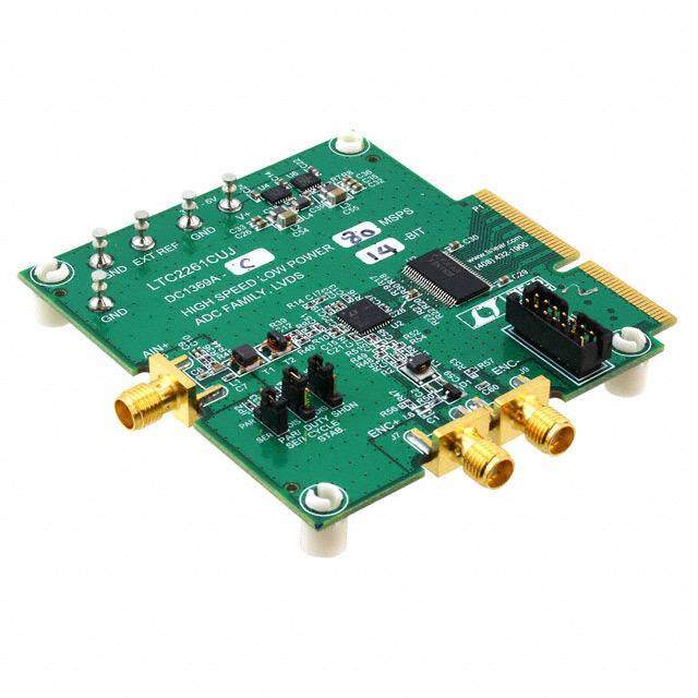
ICGOO电子元器件商城为您提供DC1369A-C由LINEAR TECHNOLOGY设计生产,在icgoo商城现货销售,并且可以通过原厂、代理商等渠道进行代购。 DC1369A-C价格参考¥1543.26-¥1653.50。LINEAR TECHNOLOGYDC1369A-C封装/规格:评估板 - 模数转换器(ADC), LTC2259-14 - 14 Bit 80M Samples per Second Analog to Digital Converter (ADC) Evaluation Board。您可以下载DC1369A-C参考资料、Datasheet数据手册功能说明书,资料中有DC1369A-C 详细功能的应用电路图电压和使用方法及教程。
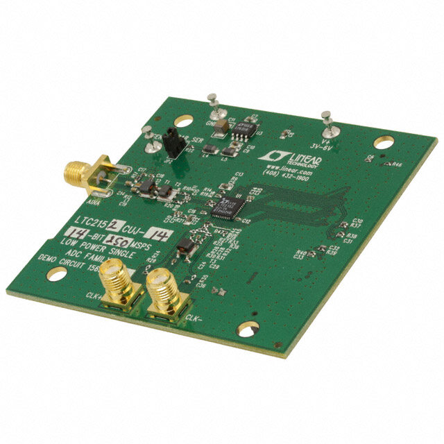
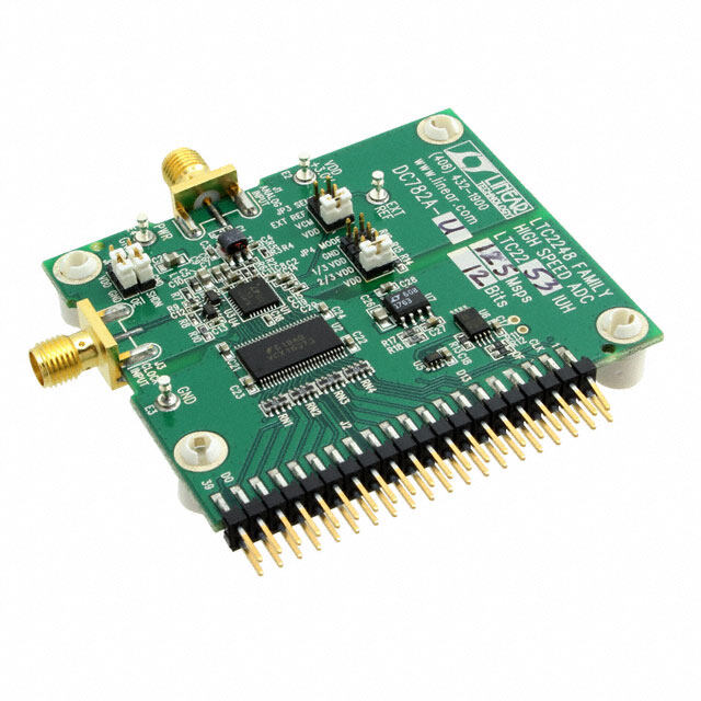
DC1369A-C是Linear Technology(现为Analog Devices公司产品线)推出的一款评估板,专用于LTC2380-24型模数转换器(ADC)的性能测试与开发验证。该评估板主要面向高精度、高速数据采集系统的研发场景,适用于需要24位分辨率和高达500 kSPS采样率的应用领域。

典型应用场景包括精密工业测量设备、高保真音频处理系统、科学仪器(如光谱仪、质谱仪)、医疗成像设备以及地震监测等对信号精度要求极高的场合。DC1369A-C支持差分输入和单端输入模式,具备低噪声电源设计和优化的模拟前端电路,能够充分展现LTC2380-24的优异动态性能(如高SNR和低失真),便于工程师评估其在真实环境中的表现。

此外,该评估板兼容Linduino开发平台,支持通过USB接口连接PC,配合专用软件进行数据采集、频谱分析和时域波形观察,极大简化了系统调试与算法验证过程。因此,DC1369A-C广泛应用于高端ADC的技术预研、原型设计及教学实验中,是开发高精度数据转换系统的理想工具。
| 参数 | 数值 |
| ADC数 | 1 |
| 产品目录 | 编程器,开发系统 |
| 描述 | BOARD DEMO 80MSPS LTC2259-14 |
| 产品分类 | 评估板 - 模数转换器 (ADC) |
| 品牌 | Linear Technology |
| 数据手册 | http://www.linear.com/docs/26930点击此处下载产品Datasheet |
| 产品图片 |
|
| 产品型号 | DC1369A-C |
| rohs | 无铅 / 符合限制有害物质指令(RoHS)规范要求 |
| 产品系列 | PScope™ |
| 不同条件下的功率(典型值) | 170mW @ 80MSPS |
| 位数 | 14 |
| 使用的IC/零件 | LTC2259-14 |
| 其它名称 | DC1369AC |
| 工作温度 | 0°C ~ 70°C |
| 所含物品 | 板 |
| 数据接口 | 并联 |
| 标准包装 | 1 |
| 相关产品 | /product-detail/zh/DC890B/DC890B-ND/2552648/product-detail/zh/LTC2259IUJ-14%23TRPBF/LTC2259IUJ-14%23TRPBF-ND/2002093/product-detail/zh/LTC2259CUJ-14%23TRPBF/LTC2259CUJ-14%23TRPBF-ND/2002092/product-detail/zh/LTC2259IUJ-12%23TRPBF/LTC2259IUJ-12%23TRPBF-ND/2002091/product-detail/zh/LTC2259CUJ-12%23TRPBF/LTC2259CUJ-12%23TRPBF-ND/2002090/product-detail/zh/LTC2259IUJ-14%23PBF/LTC2259IUJ-14%23PBF-ND/1990609/product-detail/zh/LTC2259IUJ-12%23PBF/LTC2259IUJ-12%23PBF-ND/1990608/product-detail/zh/LTC2259CUJ-14%23PBF/LTC2259CUJ-14%23PBF-ND/1990607/product-detail/zh/LTC2259CUJ-12%23PBF/LTC2259CUJ-12%23PBF-ND/1990606 |
| 设计资源 | http://cds.linear.com/docs/39921 |
| 软件下载 | http://ltspice.linear.com/software/ltcps.exe |
| 输入范围 | 1 ~ 2 Vpp |
| 采样率(每秒) | 80M |


- 商务部:美国ITC正式对集成电路等产品启动337调查
- 曝三星4nm工艺存在良率问题 高通将骁龙8 Gen1或转产台积电
- 太阳诱电将投资9.5亿元在常州建新厂生产MLCC 预计2023年完工
- 英特尔发布欧洲新工厂建设计划 深化IDM 2.0 战略
- 台积电先进制程称霸业界 有大客户加持明年业绩稳了
- 达到5530亿美元!SIA预计今年全球半导体销售额将创下新高
- 英特尔拟将自动驾驶子公司Mobileye上市 估值或超500亿美元
- 三星加码芯片和SET,合并消费电子和移动部门,撤换高东真等 CEO
- 三星电子宣布重大人事变动 还合并消费电子和移动部门
- 海关总署:前11个月进口集成电路产品价值2.52万亿元 增长14.8%

PDF Datasheet 数据手册内容提取
DEMO MANUAL DC1369A LTC2262-14/-12, LTC2261-14/-12, LTC2260-14/-12, LTC2259-14/-12, LTC2258-14/-12, LTC2257-14/-12, LTC2256-14/-12, 14/12-Bit, 25Msps to 150Msps ADCs Description Demonstration circuit 1369A supports a family of Several versions of the 1369A demo board supporting the 14/12-bit 25Msps to 150Msps ADCs. Each assembly LTC2261 14/12-bit series of A/D converters are listed in features one of the following devices: LTC2262-14 or Table 1. Depending on the required resolution and sample LTC2262-12, LTC2261-14, LTC2261-12, LTC2260-14, rate, the DC1369A is supplied with the appropriate ADC. LTC2260-12, LTC2259-14, LTC2259-12, LTC2258-14, The circuitry on the analog inputs is optimized for analog LTC2258-12, LTC2257-14, LTC2257-12, LTC2256-14, input frequencies from 5MHz to 170MHz. Refer to the LTC2256-12, high speed, high dynamic range ADCs. data sheet for proper input networks for different input frequencies. Demonstration circuit 1369A supports the LTC2261 family DDR LVDS output mode. This family of ADCs is also sup- Design files for this circuit board are available at ported by demonstration circuit 1370A, which is compatible http://www.linear.com/demo with CMOS and DDR CMOS output modes. L, LT, LTC, LTM, Linear Technology and the Linear logo are registered trademarks and PScope and QuikEval are trademarks of Linear Technology Corporation. All other trademarks are the property of their respective owners. performance summary (T = 25°C) A Table 1 PARAMETER CONDITION VALUE Supply Voltage – DC1369A Depending on sampling rate and the A/D converter Optimized for 3.6V provided, this supply must provide up to 250mA 3.5V ↔ 6.0V Min/Max Analog Input Range Depending on SENSE Pin Voltage 1V to 2V P-P P-P Logic Input Voltages Minimum Logic High 1.3V Maximum Logic Low 0.6V Logic Output Voltages (Differential) Nominal Logic Levels (100Ω Load, 3.5mA Mode) 350mV/1.25V Common Mode Minimum Logic Levels (100Ω Load, 3.5mA Mode) 247mV/1.25V Common Mode Sampling Frequency (Convert Clock Frequency) See Table 1 Convert Clock Level Single-Ended Encode Mode (ENC – Tied to GND) 0V to 3.6V Convert Clock Level Differential Encode Mode (ENC – Not Tied to GND) 0.2V to 3.6V Resolution See Table 1 Input Frequency Range See Table 1 SFDR See Applicable Data Sheet SNR See Applicable Data Sheet dc1369af 1
DEMO MANUAL DC1369A Quick start proceDure Table 2. DC1369A Variants DC1369A VARIANTS ADC PART NUMBER RESOLUTION MAXIMUM SAMPLE RATE INPUT FREQUENCY 1369A-A LTC2261-14 14-Bit 125Msps 5MHz to 170MHz 1369A-B LTC2260-14 14-Bit 105Msps 5MHz to 170MHz 1369A-C LTC2259-14 14-Bit 80Msps 5MHz to 170MHz 1369A-D LTC2258-14 14-Bit 65Msps 5MHz to 170MHz 1369A-E LTC2257-14 14-Bit 40Msps 5MHz to 170MHz 1369A-F LTC2256-14 14-Bit 25Msps 5MHz to 170MHz 1369A-G LTC2261-12 12-Bit 125Msps 5MHz to 170MHz 1369A-H LTC2260-12 12-Bit 105Msps 5MHz to 170MHz 1369A-I LTC2259-12 12-Bit 80Msps 5MHz to 170MHz 1369A-J LTC2258-12 12-Bit 65Msps 5MHz to 170MHz 1369A-K LTC2257-12 12-Bit 40Msps 5MHz to 170MHz 1369A-L LTC2256-12 12-Bit 25Msps 5MHz to 170MHz 1369A-M LTC2262-14 14-Bit 150Msps 5MHz to 170MHz 1369A-N LTC2262-12 12-Bit 150Msps 5MHz to 170MHz Demonstration circuit 1369A is easy to set up to evaluate Applying Power and Signals to the DC1369A the performance of the LTC2262 family of A/D converters. Demonstration Circuit Refer to Figure 1 for proper measurement equipment setup If a DC890 is used to acquire data from the DC1369A, and follow the procedure below: the DC890 must first be connected to a powered USB port or provided an external 6V to 9V before applying Setup 3.6V to 6.0V across the pins marked V+ and GND on the If a DC890 QuikEval™ II Data Acquisition and Collection DC1369A. DC1369A requires 3.6V for proper operation. System was supplied with the DC1369A demonstration Regulators on the board produce the voltages required for circuit, follow the DC890 Quick Start Guide to install the the ADC. The DC1369A demonstration circuit requires up required software and for connecting the DC890 to the to 250mA depending on the sampling rate and the A/D DC1369A and to a PC. converter supplied. The DC890 data collection board is powered by the USB DC1369A Demonstration Circuit Board Jumpers cable and does not require an external power supply unless The DC1369A demonstration circuit board should have it must be connected to the PC through an unpowered hub, the following jumper settings as default positions (as per in which case it must be supplied an external 6V to 9V on Figure 1): turrets G7(+) and G1(–) or the adjacent 2.1mm power jack. JP2: PAR/SER: Selects Parallel or Serial programming Analog Input Network mode. (Default – Serial) For optimal distortion and noise performance the RC JP3: Duty Cycle Stabilizer: Enables/Disable Duty Cycle network on the analog inputs may need to be optimized Stabilizer. (Default – Enable) for different analog input frequencies. For input frequen- JP4: SHDN: Enables and disables the LTC2262 cies above 170MHz, refer to the LTC2262 data sheet for a (Default – Enable) proper input network. Other input networks may be more appropriate for input frequencies less that 5MHz. dc1369af 2
DEMO MANUAL DC1369A Quick start proceDure 3.5V to 6V Jumpers Are Shown in + Default Positions Analog Input Parallel Data Output to DC890 Parallel/Serial Programming Mode Duty Cycle Stabilizer DC1369A F01 SHDN Single-Ended Encode Clock Figure 1. DC1369A Setup dc1369af 3
DEMO MANUAL DC1369A Quick start proceDure In almost all cases, filters will be required on both analog For the best noise performance, the encode input must input and encode clock to provide data sheet SNR. In the be driven with a very low jitter, square wave source. The case of the DC1369A a bandpass filter used for the clock amplitude should be large, up to 3V or 13dBm. When P-P should be used prior to the DC1075A. using a sinusoidal signal generator a squaring circuit can be used. Linear Technology also provides demo board The filters should be located close to the inputs to avoid DC1075A that divides a high frequency sine wave by four, reflections from impedance discontinuities at the driven producing a low jitter square wave for best results with end of a long transmission line. Most filters do not present the LTC2262 family. 50Ω outside the passband. In some cases, 3dB to 10dB pads may be required to obtain low distortion. Using bandpass filters on the clock and the analog input will improve the noise performance by reducing the If your generator cannot deliver full-scale signals without wideband noise power of the signals. In the case of the distortion, you may benefit from a medium power amplifier DC1369A a bandpass filter used for the clock should be based on a Gallium Arsenide Gain block prior to the final used prior to the DC1075A. Data sheet FFT plots are taken filter. This is particularly true at higher frequencies where with 10 pole LC filters made by TTE (Los Angeles, CA) to IC based operational amplifiers may be unable to deliver suppress signal generator harmonics, non harmonically the combination of low noise figure and High IP3 point related spurs and broadband noise. Low phase noise Agilent required. A high order filter can be used prior to this final 8644B generators are used with TTE bandpass filters for amplifier, and a relatively lower Q filter used between the both the clock input and the analog input. amplifier and the demo circuit. Apply the analog input signal of interest to the SMA con- Encode Clock nectors on the DC1369A demonstration circuit board marked J5 A +. These inputs are capacitive coupled to NOTE: Apply an encode clock to the SMA connector on IN Balun transformers ETC1-1-13. the DC1369A demonstration circuit board marked J7. As a default the DC1369A is populated to have a single- An internally generated conversion clock output is avail- ended input. able on J1 which could be collected via a logic analyzer, or other data collection system if populated with a SAMTEC MEC8-150 type connector or collected by the DC890 Qui- kEval II Data Acquisition Board using PScope™ software. dc1369af 4
DEMO MANUAL DC1369A Quick start proceDure Software Manual Configuration settings: The DC890 is controlled by the PScope System Software Bits: 14 (or 12 for 12-bit parts) provided or downloaded from the Linear Technology Alignment: 14 website at http://www.linear.com/software/. If a DC890 was provided, follow the DC890 Quick Start Guide and FPGA Ld: DDR LVDS the instructions below. Channs: 2 To start the data collection software if PScope.exe is in- Bipolar: Checked stalled (by default) in \Program Files\LTC\PScope\, double Positive-Edge Clk: Checked click the PScope Icon or bring up the run window under the start menu and browse to the PScope directory and If everything is hooked up properly, powered and a suit- select PScope. able convert clock is present, clicking the Collect button should result in time and frequency plots displayed in If the DC1369A demonstration circuit is properly connected the PScope window. Additional information and help for to the DC890, PScope should automatically detect the PScope is available in the DC890 Quick Start Guide and in DC1369A, and configure itself accordingly. If necessary the online help available within the PScope program itself. the procedure below explains how to manually configure PScope. Under the Configure menu, go to “ADC Configuration....” Check the Config Manually box and use the following configuration options (see Figure 2): Figure 2. ADC Configuration dc1369af 5
DEMO MANUAL DC1369A Quick start proceDure Serial Programming This menu allows any of the options available for the LTC2262 family to be programmed serially. The LTC2262 PScope has the ability to program the DC1369A board family has the following options: serially through the DC890. There are several options available in the LTC2262 family that are only available Power Control: Selects between normal operation, nap, through serially programming. PScope allows all of these and sleep modes features to be tested. • Normal (Default): Entire ADC is powered, and active These options are available by first clicking on the Set • Nap: ADC core powers down while references stay Demo Bd Options icon on the PScope toolbar (Figure 3). active This will bring up the menu shown in Figure 4. • Shutdown: The entire ADC is powered down Clock Inversion: Selects the polarity of the CLKOUT signal • Normal (Default): Normal CLKOUT polarity • Inverted: CLKOUT polarity is inverted Figure 3. PScope Toolbar Clock Delay: Selects the phase delay of the CLKOUT signal • None (Default): No CLKOUT delay • 45 deg: CLKOUT delayed by 45 degrees • 90 deg: CLKOUT delayed by 90 degrees • 135 deg: CLKOUT delayed by 135 degrees Clock Duty Cycle: Enable or Disables Duty Cycle Stabilizer • Stabilizer Off (Default): Duty cycle stabilizer disabled • Stabilizer On: Duty cycle stabilizer enabled Output Current: Selects the LVDS output drive current • 1.75mA (Default): LVDS output driver current • 2.1mA: LVDS output driver current • 2.5mA: LVDS output driver current Figure 4. Demo Board Configuration Options • 3.0mA: LVDS output driver current • 3.5mA: LVDS output driver current • 4.0mA: LVDS output driver current • 4.5mA: LVDS output driver current dc1369af 6
DEMO MANUAL DC1369A Quick start proceDure Internal Termination: Enables LVDS Internal Termination Alternate Bit: Alternate Bit Polarity (ABP) Mode • Off (Default): Disables internal termination • Off (Default): Disables alternate bit polarity • On: Enables internal termination • On: Enables alternate bit polarity (Before enabling ABP, be sure the part is in offset binary mode) Outputs: Enables Digital Outputs • Enabled (Default): Enables digital outputs Randomizer: Enables Data Output Randomizer • Disabled: Disables digital outputs • Off (Default): Disables data output randomizer • On: Enables data output randomizer Output Mode: Selects Digital Output Mode • Full Rate: Full rate CMOS output mode (This mode is Two’s Complement: Enables Two’s Complement Mode not supported by the DC1369A, please use the DC1370) • Off (Default): Selects offset binary mode • Double LVDS (Default): Double data rate LVDS output • On: Selects two’s complement mode mode • Double CMOS: Double data rate CMOS output mode Once the desired settings are selected hit OK and PScope (This mode is not supported by the DC1369A, please will automatically update the register of the device on the use the DC1370) DC1369A demo board. Test Pattern: Selects Digital Output Test Patterns • Off (Default): ADC data presented at output • All Out = 1: All digital outputs are 1 • All Out = 0: All digital outputs are 0 • Checkerboard: OF, and D13-D0 Alternate between 101 0101 1010 0101 and 010 1010 0101 1010 on alternat- ing samples. • Alternating: Digital outputs alternate between all 1’s and all 0’s on alternating samples. dc1369af 7
DEMO MANUAL DC1369A parts List ITEM QTY REFERENCE PART DESCRIPTION MANUFACTURER/PART NUMBER 1 1 C1 RES, 0402 150Ω 1% 1/16W VISHAY CRCW0402150RFKED 2 9 C2, C3, C6, C7, C38, C39, C59-C61 CAP, 0402 0.01uF 10% 16V X7R AVX 0402YC103KAT 3 2 C10, C9 CAP, 0402 8.2pF 5% 50V COG AVX 04025A8R2JAT2A 4 6 C12, C15, C18, C19, C21, C37 CAP, 0402 0.1uF 10% 10V X5R TDK C1005X5R1A104K 5 3 C13, C17, C23 CAP, 0402 1uF 10% 10V X5R TDK C1005X5R1A105K 6 2 C14, C22 CAP, 0603 1uF 10% 16V X7R TDK C1608X7R1C105K 7 1 C20 CAP, 0402 1uF 10% 10V X5R MURATA GRM155R61A105KE15D 8 1 C24 CAP, 0603 4.7uF 20% 6.3V X5R TDK C1608X5R0J475MT 9 12 C26-C36, C56 CAP, 0603 0.1uF 10% 50V X7R TDK C1608X7R1H104K 10 1 C51 CAP, 0402 4.7pF +/-0.25pF 50V NPO AVX 04025A4R7CAT2A 11 2 C53, C52 CAP, 0402 100pf 5% 50V COG TDK C1005C0G1H101J 12 2 C54, C55 CAP, 1206 22uF 10% 6.3V X5R AVX 12066D226KAT2A 13 7 R9, R10, R48, R54, R57, C57, C58 RES, 0402 0Ω JUMPER VISHAY CRCW04020000Z0ED 14 1 D1 DIODE, SCHOTTKY SOT-23 AVAGO HSMS-2822 15 3 JP2, JP3, JP4 HEADER, 3-PIN, 2mm SAMTEC TMM-103-02-L-S 16 3 J5, J7, J9 CONN, BNC, SMA 50Ω EDGE-LANCH E.F.JOHNSON, 142-0701-851 17 1 J8 HEADER, 2×7 2mm MOLEX 87331-1420 18 1 L1 IND, 0603 56uH 5% MURATA LQP18MN56NG02D 19 3 L2, L3, L4 FERRITE BEAD, 1206 MURATA BLM31PG330SN1L 20 1 L5 IND, 0603 BEAD ? 21 1 L6 IND, 0603 OPTION OPTION 22 1 P1 EDGE FINGERS ON PCB PART OF THE PCB 23 2 RN2, RN1 RES ARRAY, 33Ω VISHAY CRA04SS08333R0JTD 24 2 R1, R2 RES, 0402 301Ω 1% 1/16W VISHAY CRCW0402301RFKED 25 3 R4, R5, R56 RES, 0402 OPTION OPTION 26 1 R6 RES, 0402 10kΩ 5% 1/16W VISHAY CRCW040210K0JNED 27 1 R7 RES, 0402 10kΩ 1% 1/16W VISHAY CRCW040210K0FKED 28 1 R8 RES, 0402 6.81kΩ 1% 1/16W YAGEO RC0402FR-076K81L 29 4 R14, R33, R34, R35 RES, 0402 1kΩ 5% 1/16W VISHAY CRCW04021K00JNTDE3 30 1 R16 RES, 0402 100Ω 5% 1/16W VISHAY CRCW0402100RJNED 31 8 R17-R23, R30 RES, 0201 100Ω 5% 1/16W VISHAY CRCW0201100RFNTD 32 1 R24 RES, 0402 100kΩ 5% 1/16W VISHAY CRCW0402100KJNED 33 3 R25, R26, R29 RES, 0603 4.99kΩ 1% 1/16W AAC CR16-4991FM 34 3 R36, R44, R45 RES, 0402 86.6Ω 1% 1/16W VISHAY CRCW040286R6FKED 35 2 R40, R39 RES, 0402 24.9Ω 1% 1/16W VISHAY CRCW040224R9FKED 36 0 R46, R49, R52, R53, R55 RES, 0402 OPTION VISHAY CRCW0402101J ? 37 1 R47 RES, 0402 20Ω 1% 1/16W VISHAY CRCW040220R0FKED 38 1 R50 IND, 36nH COILCRAFT 0402CS-36NXJB 39 0 R51 RES, 0402 301Ω 1% 1/16W OPTION VISHAY CRCW0402301RFKED OPTION 40 5 TP1, TP2, TP3, TP4, TP5 TURRETS MILLMAX 2501-2-00-80-00-00-07-0 41 1 T1 XFMR, 1:1 MACOM MABA-007159-000000 42 1 T2 XFMR, 1:1 CT M/A-C0M MABAES0060/COILCRAFT WBC1-1LB dc1369af 8
DEMO MANUAL DC1369A parts List ITEM QTY REFERENCE PART DESCRIPTION MANUFACTURER/PART NUMBER 43 1 T3 XFMR, 1:4 CT COILCRAFT WBC4-1WLB 44 1 U1 IC, EEPROM MICROCHIP TECH. 24LC025-I/ST 45 1 U3 IC, FIN1108 FAIRCHILD FIN1108 46 1 U4 IC, LDO Micropower Regulators LINEAR TECH. LT1763CDE-1.8 47 1 U5 IC, 8-BIT I/0 EXPANDER PHILIPS SEMI PCF8574TS/3 48 1 U6 IC, LDO Micropower Regulators LINEAR TECH. LT1763CDE 49 1 U7 IC, EEPROM MICROCHIP TECH. 24LC32A-I/ST 50 3 XJP2, XJP3, XJP4 SHUNT, 2mm SAMTEC 2SN-BK-G 51 4 STANDOFF, SNAP ON KEYSTONE_8831 See page 2 of the Schematic Diagram for U2. dc1369af 9
DEMO MANUAL DC1369A schematic Diagram D C B A 21REVISION HISTORYREVISION HISTORYREVISION HISTORYDESCRIPTIONDATEAPPROVEDECOREVDESCRIPTIONDATEAPPROVEDECOREVDESCRIPTIONDATEAPPROVEDECOREV 333PROTO08/11/08PROTO08/11/08PROTO08/11/08 Change3.105/22/12Clarence M. VOUT 2568712244P1EDGE-CON-100P1EDGE-CON-100U3U3FIN1108FIN110812354CCCCC21VVVVV343EN122265EN342787EN5646109EN78131211ENABLEEN14131615445+D12/D13IN1-OUT1-5441817-D12/D13IN1+OUT1+6432019+D10/D11IN2+OUT2+7422221-D10/D11IN2-OUT2-8412423+D8/D9IN3-OUT3-9402625-D8/D9IN3+OUT3+10392827+CLKIN4+OUR4+30291138-CLKIN4-OUT4-14353231+D6/D7IN5-OUT5-15343433-D6/D7IN5+OUT5+16333635+D4/D5IN6+OUT6+32173837-D4/D5OUT6-IN6-18314039+D2/D3IN7-OUT7-19304241-D2/D3IN7+OUT7+44432029+D0/D1IN8+OUT8+21284645-D0/D0IN8-OUT8-48475049245251VBB123455453EEEEEVVVVV565558571236760592336261646366656867706972717473767578778079828184838685VSS8887SCL90899291SDA9493VCC_IN9695R294.99K1%R294.99K1%9897R23R23VOUT10099100100ENABLE R24R24100K100K C560.1uFC560.1uF U724LC32A-I/STU724LC32A-I/ST18VCC_INA0VCC27VSSA1WP36SCLA2SCL45SDAA3SDAOXA2 J8J81VUNREG25VRN133RN133FAST DAACS BOARD ID CIRCUITRY618VSSCSCS427SCKSCK/SCL736SDIMOSI/SDA545SD0C270.1uFC270.1uFMISOVCC_IN10C53C53C52C52EEVCC91%1%EESDA11100pF100pF100pF100pFU124LC025-I/STU124LC025-I/STR254.99KR254.99KEESCL1812SCLA0VCCEEGND27A1WP36SCLA2SCL45SDADDDA3SDA14OXA0NNNNCGGGR264.99K1%R264.99K1%SDAVCC_IN833SDA1SCLVSS CONTRACT NO.CONTRACT NO.CONTRACT NO.1630 McCarthy Blvd.1630 McCarthy Blvd.1630 McCarthy Blvd.Milpitas, CA 95035Milpitas, CA 95035Milpitas, CA 95035Phone: (408)432-1900Phone: (408)432-1900Phone: (408)432-1900APPROVALSAPPROVALSAPPROVALSDATEDATEDATETECHNOLOGYTECHNOLOGYTECHNOLOGYFax: (408)434-0507Fax: (408)434-0507Fax: (408)434-0507DRAWNDRAWNDRAWNMI10/31/07MI10/31/07MI10/31/07TITLETITLETITLECHECKEDCHECKEDCHECKEDSCH, LTC2261CUJ, HIGH SPEED LOW POWERSCH, LTC2261CUJ, HIGH SPEED LOW POWERSCH, LTC2261CUJ, HIGH SPEED LOW POWERAPPROVEDAPPROVEDAPPROVED125MSPS ADC FAMILY, LVDS125MSPS ADC FAMILY, LVDS125MSPS ADC FAMILY, LVDSENGINEERENGINEERENGINEERSIZESIZESIZECAGE CODECAGE CODECAGE CODEDWG NODWG NODWG NOREVREVREVDESIGNERDESIGNERDESIGNERDC1369ADC1369ADC1369A3.13.13.1 05/22/12 05:59:3905/22/12 05:59:3905/22/12 05:59:39NONENONENONESCALE:FILENAME:SCALE:FILENAME:SCALE:FILENAME:222SHEET1369A-3.DSNSHEET1369A-3.DSNSHEET1369A-3.DSNOF1OF1OF121 R22R22100100 R20R20100100R21R21100100 VDD R35R351K1KJP4JP41 2SDI 3 SHDNSHDN VOUT R6R6 10K10K ENEN DISDIS SCKSDISD0 CS 543This circuit is proprietary to Linear Technology and suppliedThis circuit is proprietary to Linear Technology and suppliedThis circuit is proprietary to Linear Technology and suppliedfor use with Linear Technology parts.for use with Linear Technology parts.for use with Linear Technology parts.VDDCustomer Notice:Customer Notice:Customer Notice:Linear Technology has made a best effort toLinear Technology has made a best effort toLinear Technology has made a best effort todesign a circuit that meets customer-supplied specifications;design a circuit that meets customer-supplied specifications;design a circuit that meets customer-supplied specifications;however, it remains the customers responsibility to verify properhowever, it remains the customers responsibility to verify properhowever, it remains the customers responsibility to verify properR14R14and reliable operation in the actual application, Componentand reliable operation in the actual application, Componentand reliable operation in the actual application, Component1K1Ksubstitution and printed circuit board layout may significantlysubstitution and printed circuit board layout may significantlysubstitution and printed circuit board layout may significantlyTP1TP1affect circuit performance or reliability. Contact Linearaffect circuit performance or reliability. Contact Linearaffect circuit performance or reliability. Contact LinearApplications Engineering for assistance.Applications Engineering for assistance.Applications Engineering for assistance.EXT REFEXT REFC17C17R90R90 1uF1uFR4586.61%R4586.61% T1T1R39R39R17R17MABA-007159-000000MABA-007159-00000024.924.9T2T2C6C6L1L156uH56uH1%1%100100MABAES0060MABAES0060J5J512AIN+AIN+0.01uF0.01uFC13C13C12C12R44R44R36R36R18R182R40R401uF1uFC7C786.686.686.686.610010024.924.90.1uF0.1uF1%1%1%1%1%1%0.01uF0.01uF1R16R16C10C10C9C9100100C23C238.2pF8.2pF8.2pF8.2pFR19R191001001uF1uFVDDVDDR100R100 C51C5113924576803333333334C33C33C19C19C26C26C18C18MFED---+++F13FE13SD4.7pF4.7pFC11O11ORNV__V__1300.1uF0.1uF0.1uF0.1uF0.1uF0.1uF0.1uF0.1uFVE0202AIN+D8_9+11S11DDDD229AIN-D8_9-R30R30328100100GNDCLKOUT+VOUTC15C15427REFHCLKOUT-5260.1uF0.1uFOVDDREFHOVDDC35C35C36C36C30C30C32C32C31C31C34C34C28C28C29C29C20C20625REFLOGND0.1uF0.1uF0.1uF0.1uF0.1uF0.1uF0.1uF0.1uF0.1uF0.1uF0.1uF0.1uFC21C210.1uF0.1uF0.1uF0.1uF1uF1uF724REFLD6_7+8230.1uF0.1uFPAR/SERD6_7-922PAR/SERTP4TP4VDDD4_5+1021VDDGNDVDDVDDD4_5-L5L5R46OPTR46OPT++--+-1133DOCCK____IU2U2N**SNNCDD0022G2CDDDDEESSSBEADBEADC61C610.01uF0.01uF12345678901R480R480R470R470111111111241 R56R56R49R49OPTOPTR5OPTR5OPTOPTOPTC57C5712T3T3R2R2K0R5036nHR5036nHWBC4-1WLWBC4-1WL301301L6L6J7J7C20.01uFC20.01uFISCDD1%1%ENC+ENC+CSSSR51R51OPTOPTOPTOPT3C58C58212C3C3212R1R1C1C12C59C590.01uF0.01uF301301D1D11OPTOPT1%1%HSMS-2822HSMS-282210.01uF0.01uFR52R521OPTOPTR4OPTR4OPTR55OPTR55OPTJ9J9ENC-ENC-2C60C60R540R540R53OPTR53OPTR57R57000.01uF0.01uF1 OVDDVDDVINU4LT1763CDE-1.8U4LT1763CDE-1.8VDDVDDL2L2TP2TP2102V+V+INOUT113INOUTC24C24BEADBEADC14C14C54C543.5V - 6V3.5V - 6V512R34R34R33R33L4L4SENSENCTP3TP311K1KC38C381K1K4.7uF4.7uF1uF1uF22uF22uFNC4GNDGNDJP2JP2NC90.01uF0.01uFBEADBEADC37C37JP3JP3NC6110.1uF0.1uFBYPPARPARENEN7228CSPAR/SERTP5TP5GNDSHDNGNDGND33VOUTSERSERDISDISL3BEADL3BEADU6LT1763CDEU6LT1763CDEPAR/SERPAR/SERDUTY CYCLE STAB.DUTY CYCLE STAB.102R86.81K1%R86.81K1%R710K1%R710K1%INOUT113INOUTC22C22512SENSENC1VOUT1uF1uFNC4C39C39C55C55NC9U5U5NC6PCF8574TS/3PCF8574TS/30.01uF0.01uF22uF22uFBYP5RN233RN2331071818DP0INTGNDSHDN1127DP1V12236SCLP2SCL45144SDAP3SDA163P4NC178P5NC19P6206P7A0718DA1NC913NA2NCGOX4051 543 D C B A dc1369af 10
DEMO MANUAL DC1369A schematic Diagram D C B A VVV111 RERERE3.3.3. 222 RRR EEE FFF WWW OOO OOO PPP 1 1630 McCarthy Blvd.1630 McCarthy Blvd.1630 McCarthy Blvd.Milpitas, CA 95035Milpitas, CA 95035Milpitas, CA 95035Phone: (408)432-1900Phone: (408)432-1900Phone: (408)432-1900Fax: (408)434-0507Fax: (408)434-0507Fax: (408)434-0507 EED LOW EED LOW EED LOW Y, LVDSY, LVDSY, LVDS 369A369A369A 222SHEETSHEETSHEET 1 GYGYGY SPSPSPMILMILMIL C1C1C1 OOO H H H AAA DDD NNN TECHNOLTECHNOLTECHNOL 261CUJ, HIG261CUJ, HIG261CUJ, HIGMSPS ADC FMSPS ADC FMSPS ADC F DWG NODWG NODWG NO NAME:NAME:NAME:1369A-3.DS1369A-3.DS1369A-3.DS 2 TC2TC2TC2125125125 ODEODEODE FILEFILEFILE 2 LLL CCC CTURE PCB AND OFFS TITLETITLETITLESCH, SCH, SCH, SIZECAGE SIZECAGE SIZECAGE NONENONENONESCALE:SCALE:SCALE: ANUFA X1X1 1 X2X2 1 X3X3 1 X4X4 1 NTS ST DATEDATEDATE 10/31/0710/31/0710/31/07 M E 3 USED TO REPRES CONTRACT NO.CONTRACT NO.CONTRACT NO. APPROVALSAPPROVALSAPPROVALSDRAWNDRAWNDRAWNMIMIMICHECKEDCHECKEDCHECKED APPROVEDAPPROVEDAPPROVED ENGINEERENGINEERENGINEER DESIGNERDESIGNERDESIGNER 05/22/12 06:00:3305/22/12 06:00:3305/22/12 06:00:33 3 R Y 0 0 0 0 0 0 0 0 0 0 0 0 0 0 C 7 7 7 7 7 7 7 7 7 7 7 7 7 7 EN < 1 < 1 < 1 < 1 < 1 < 1 < 1 < 1 < 1 < 1 < 1 < 1 < 1 < 1 U N N N N N N N N N N N N N N REQ < AI < AI < AI < AI < AI < AI < AI < AI < AI < AI < AI < AI < AI < AI F 5 5 5 5 5 5 5 5 5 5 5 5 5 5 S 54 This circuit is proprietary to Linear Technology and suppliedThis circuit is proprietary to Linear Technology and suppliedThis circuit is proprietary to Linear Technology and suppliedfor use with Linear Technology parts.for use with Linear Technology parts.for use with Linear Technology parts.Customer Notice:Customer Notice:Customer Notice:Linear Technology has made a best effort toLinear Technology has made a best effort toLinear Technology has made a best effort todesign a circuit that meets customer-supplied specifications;design a circuit that meets customer-supplied specifications;design a circuit that meets customer-supplied specifications;however, it remains the customers responsibility to verify properhowever, it remains the customers responsibility to verify properhowever, it remains the customers responsibility to verify properand reliable operation in the actual application, Componentand reliable operation in the actual application, Componentand reliable operation in the actual application, Componentsubstitution and printed circuit board layout may significantlysubstitution and printed circuit board layout may significantlysubstitution and printed circuit board layout may significantlyaffect circuit performance or reliability. Contact Linearaffect circuit performance or reliability. Contact Linearaffect circuit performance or reliability. Contact LinearApplications Engineering for assistance.Applications Engineering for assistance.Applications Engineering for assistance. * No. of BITSAMPLE RATEASSYADC LTC2261-1414125Msps-A LTC2160-1414-B105Msps LTC2259-1414-C80Msps LTC2258-1414-D65Msps LTC2257-1414-E40Msps LTC2256-1414-F25Msps LTC2261-1212-G125Msps 12LTC2260-12-H105Msps 12-ILTC2259-1280Msps 12LTC2258-12-J65Msps LTC2257-1212-K40Msps 12LTC2256-12-L25Msps 150Msps-M14LTC2262-14 12LTC2262-12-N150Msps 54 D C B A dc1369af 11 Information furnished by Linear Technology Corporation is believed to be accurate and reliable. However, no responsibility is assumed for its use. Linear Technology Corporation makes no representa- tion that the interconnection of its circuits as described herein will not infringe on existing patent rights.
DEMO MANUAL DC1369A DEMONSTRATION BOARD IMPORTANT NOTICE Linear Technology Corporation (LTC) provides the enclosed product(s) under the following AS IS conditions: This demonstration board (DEMO BOARD) kit being sold or provided by Linear Technology is intended for use for ENGINEERING DEVELOPMENT OR EVALUATION PURPOSES ONLY and is not provided by LTC for commercial use. As such, the DEMO BOARD herein may not be complete in terms of required design-, marketing-, and/or manufacturing-related protective considerations, including but not limited to product safety measures typically found in finished commercial goods. As a prototype, this product does not fall within the scope of the European Union directive on electromagnetic compatibility and therefore may or may not meet the technical requirements of the directive, or other regulations. If this evaluation kit does not meet the specifications recited in the DEMO BOARD manual the kit may be returned within 30 days from the date of delivery for a full refund. THE FOREGOING WARRANTY IS THE EXCLUSIVE WARRANTY MADE BY THE SELLER TO BUYER AND IS IN LIEU OF ALL OTHER WARRANTIES, EXPRESSED, IMPLIED, OR STATUTORY, INCLUDING ANY WARRANTY OF MERCHANTABILITY OR FITNESS FOR ANY PARTICULAR PURPOSE. EXCEPT TO THE EXTENT OF THIS INDEMNITY, NEITHER PARTY SHALL BE LIABLE TO THE OTHER FOR ANY INDIRECT, SPECIAL, INCIDENTAL, OR CONSEQUENTIAL DAMAGES. The user assumes all responsibility and liability for proper and safe handling of the goods. Further, the user releases LTC from all claims arising from the handling or use of the goods. Due to the open construction of the product, it is the user’s responsibility to take any and all appropriate precautions with regard to electrostatic discharge. Also be aware that the products herein may not be regulatory compliant or agency certified (FCC, UL, CE, etc.). No License is granted under any patent right or other intellectual property whatsoever. LTC assumes no liability for applications assistance, customer product design, software performance, or infringement of patents or any other intellectual property rights of any kind. LTC currently services a variety of customers for products around the world, and therefore this transaction is not exclusive. Please read the DEMO BOARD manual prior to handling the product. Persons handling this product must have electronics training and observe good laboratory practice standards. Common sense is encouraged. This notice contains important safety information about temperatures and voltages. For further safety concerns, please contact a LTC applica- tion engineer. Mailing Address: Linear Technology 1630 McCarthy Blvd. Milpitas, CA 95035 Copyright © 2004, Linear Technology Corporation dc1369af 12 Linear Technology Corporation LT 0612 • PRINTED IN USA 1630 McCarthy Blvd., Milpitas, CA 95035-7417 (408) 432-1900 ● FAX: (408) 434-0507 ● www.linear.com LINEAR TECHNOLOGY CORPORATION 2012