ICGOO在线商城 > 集成电路(IC) > 数据采集 - 数模转换器 > DAC902E
 Datasheet下载
- 型号: DAC902E
- 制造商: Texas Instruments
- 库位|库存: xxxx|xxxx
- 要求:
| 数量阶梯 | 香港交货 | 国内含税 |
| +xxxx | $xxxx | ¥xxxx |
查看当月历史价格
查看今年历史价格
DAC902E产品简介:
ICGOO电子元器件商城为您提供DAC902E由Texas Instruments设计生产,在icgoo商城现货销售,并且可以通过原厂、代理商等渠道进行代购。 DAC902E价格参考¥54.22-¥90.85。Texas InstrumentsDAC902E封装/规格:数据采集 - 数模转换器, 12 位 数模转换器 1 28-TSSOP。您可以下载DAC902E参考资料、Datasheet数据手册功能说明书,资料中有DAC902E 详细功能的应用电路图电压和使用方法及教程。
Texas Instruments(德州仪器)的DAC902E是一款12位电压输出数模转换器(DAC),适用于多种需要高精度模拟信号生成的应用场景。以下是该型号的一些典型应用场景:

 1. 工业自动化与控制
   DAC902E常用于工业控制系统中,如PLC(可编程逻辑控制器)、DCS(分布式控制系统)等。它能够将数字信号转换为精确的模拟电压输出,用于控制电机、阀门、传感器等设备的运行状态。例如,在温度、压力或流量控制回路中,DAC902E可以提供高精度的控制信号,确保系统的稳定性和响应速度。

 2. 测试与测量设备
   在精密测试仪器中,DAC902E可以用于生成标准的电压信号,作为参考源或激励信号。例如,示波器、信号发生器、万用表等设备可以通过DAC902E生成精确的模拟信号,用于校准或测试其他电子设备的性能。其12位分辨率和低噪声特性使得它非常适合用于要求高精度的测量应用。

 3. 音频处理与合成
   DAC902E也可应用于音频设备中,特别是在需要高质量音频信号生成的场合。它可以将数字音频信号转换为模拟电压信号,驱动扬声器或耳机。由于其较高的分辨率和线性度,DAC902E能够提供清晰、无失真的音频输出,适用于专业音频设备、音乐合成器等领域。

 4. 医疗设备
   在医疗领域,DAC902E可用于各种诊断和治疗设备中,如心电图机、超声设备、监护仪等。这些设备通常需要精确的模拟信号来驱动传感器或生成刺激信号。DAC902E的高精度和稳定性使其能够在这些关键应用中发挥重要作用,确保设备的准确性和安全性。

 5. 通信系统
   在通信领域,DAC902E可以用于调制解调器、无线发射机等设备中,生成所需的模拟信号以实现数据传输。它的低功耗和小尺寸设计使其非常适合便携式通信设备,同时其高精度特性也有助于提高通信质量。

总之,DAC902E凭借其高精度、低功耗和广泛的适用性,广泛应用于工业、医疗、通信、音频等多个领域,满足了不同行业对高精度模拟信号生成的需求。
| 参数 | 数值 |
| 产品目录 | 集成电路 (IC)半导体 |
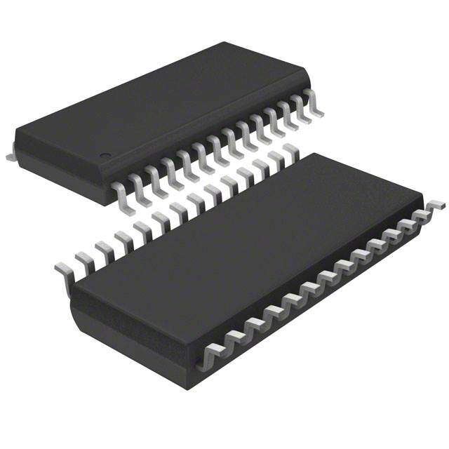
| 描述 | IC 12-BIT D/A CONV 28-TSSOP数模转换器- DAC 12-Bit 165MSPS SpeedPlus DAC |
| 产品分类 | |
| 品牌 | Texas Instruments |
| 产品手册 | |
| 产品图片 |
|
| rohs | 符合RoHS无铅 / 符合限制有害物质指令(RoHS)规范要求 |
| 产品系列 | 数据转换器IC,数模转换器- DAC,Texas Instruments DAC902ESpeedPlus™ |
| 数据手册 | |
| 产品型号 | DAC902E |
| 产品培训模块 | http://www.digikey.cn/PTM/IndividualPTM.page?site=cn&lang=zhs&ptm=13240 |
| 产品目录页面 | |
| 产品种类 | 数模转换器- DAC |
| 位数 | 12 |
| 供应商器件封装 | 28-TSSOP |
| 分辨率 | 12 bit |
| 制造商产品页 | http://www.ti.com/general/docs/suppproductinfo.tsp?distId=10&orderablePartNumber=DAC902E |
| 包装 | 管件 |
| 单位重量 | 117.500 mg |
| 商标 | Texas Instruments |
| 安装类型 | 表面贴装 |
| 安装风格 | SMD/SMT |
| 封装 | Tube |
| 封装/外壳 | 28-TSSOP(0.173",4.40mm 宽) |
| 封装/箱体 | TSSOP-28 |
| 工作温度 | -40°C ~ 85°C |
| 工厂包装数量 | 50 |
| 建立时间 | 30ns |
| 接口类型 | Parallel |
| 数据接口 | 并联 |
| 最大工作温度 | + 85 C |
| 最小工作温度 | - 40 C |
| 标准包装 | 50 |
| 电压参考 | Internal or External |
| 电压源 | 模拟和数字 |
| 电源电压-最大 | 5.5 V |
| 电源电压-最小 | 2.7 V |
| 积分非线性 | +/- 2.5 LSB |
| 稳定时间 | 30 ns |
| 系列 | DAC902 |
| 结构 | Current Steering |
| 转换器数 | 1 |
| 转换器数量 | 1 |
| 输出数和类型 | 2 电流,单极 |
| 输出类型 | Current |
| 配用 | /product-detail/zh/DEM-DAC90XU/296-9470-ND/379765 |
| 采样比 | 200 MSPs |
| 采样率(每秒) | 200M |


PDF Datasheet 数据手册内容提取
DAC902 D A C 9 0 2 DAC902 SBAS094B – MAY 2002 12-Bit, 165MSPS TM DIGITAL-TO-ANALOG CONVERTER FEATURES APPLICATIONS (cid:1) SINGLE +5V OR +3V OPERATION (cid:1) COMMUNICATION TRANSMIT CHANNELS: (cid:1) HIGH SFDR: 5MHz Output at 100MSPS: 67dBc WLL, Cellular Base Station Digital Microwave Links (cid:1) LOW GLITCH: 3pV-s Cable Modems (cid:1) LOW POWER: 170mW at +5V (cid:1) WAVEFORM GENERATION: (cid:1) INTERNAL REFERENCE: Direct Digital Synthesis (DDS) Arbitrary Waveform Generation (ARB) Optional Ext. Reference Adjustable Full-Scale Range (cid:1) MEDICAL/ULTRASOUND Multiplying Option (cid:1) HIGH-SPEED INSTRUMENTATION AND CON- TROL (cid:1) VIDEO, DIGITAL TV DESCRIPTION For noncontinuous operation of the DAC902, a power-down mode results in only 45mW of standby power. The DAC902 is a high-speed, Digital-to-Analog Converter (DAC) The DAC902 comes with an integrated 1.24V bandgap reference offering a 12-bit resolution option within the SpeedPlus Family of and edge-triggered input latches, offering a complete converter high-performance converters. Featuring pin compatibility among solution. Both +3V and +5V CMOS logic families can be inter- family members, the DAC908, DAC900, and DAC904 provide a faced to the DAC902. component selection option to an 8-, 10-, and 14-bit resolution, The reference structure of the DAC902 allows for additional respectively. All models within this family of DACs support update flexibility by utilizing the on-chip reference, or applying an exter- rates in excess of 165MSPS with excellent dynamic performance, nal reference. The full-scale output current can be adjusted over a and are especially suited to fulfill the demands of a variety of span of 2mA to 20mA, with one external resistor, while maintain- applications. ing the specified dynamic performance. The advanced segmentation architecture of the DAC902 is opti- The DAC902 is available in the SO-28 and TSSOP-28 packages. mized to provide a high Spurious-Free Dynamic Range (SFDR) for single-tone, as well as for multi-tone signals—essential when used for the transmit signal path of communication systems. +VA BW +VD The DAC902 has a high impedance (200kΩ) current output with a DAC902 nominal range of 20mA and an output compliance of up to 1.25V. IOUT LSB The differential outputs allow for both a differential or single- FSA Switches IOUT Current BYP ended analog signal interface. The close matching of the current outputs ensures superior dynamic performance in the differential REFIN Sources Segmented Switches configuration, which can be implemented with a transformer. Utilizing a small geometry CMOS process, the monolithic DAC902 INT/EXT can be operated on a wide, single-supply range of +2.7V to +5.5V. Latches PD Its low power consumption allows for use in portable and battery- +1.24V Ref. operated systems. Further optimization can be realized by lowering 12-Bit Data Input the output current with the adjustable full-scale option. AGND CLK D11...D0 DGND Please be aware that an important notice concerning availability, standard warranty, and use in critical applications of Texas Instruments semiconductor products and disclaimers thereto appears at the end of this data sheet. PRODUCTION DATA information is current as of publication date. Copyright © 2002, Texas Instruments Incorporated Products conform to specifications per the terms of Texas Instruments standard warranty. Production processing does not necessarily include testing of all parameters. www.ti.com
ABSOLUTE MAXIMUM RATINGS ELECTROSTATIC +V to AGND........................................................................–0.3V to +6V DISCHARGE SENSITIVITY A +V to DGND........................................................................–0.3V to +6V D AGND to DGND.................................................................–0.3V to +0.3V This integrated circuit can be damaged by ESD. Texas Instru- +V to +V ...............................................................................–6V to +6V A D ments recommends that all integrated circuits be handled with CLK, PD to DGND.....................................................–0.3V to V + 0.3V D D0-D11 to DGND.......................................................–0.3V to V + 0.3V appropriate precautions. Failure to observe proper handling D I , I to AGND........................................................–1V to V + 0.3V and installation procedures can cause damage. OUT OUT A BW, BYP to AGND.....................................................–0.3V to V + 0.3V A ESD damage can range from subtle performance degradation REF , FSA to AGND.................................................–0.3V to V + 0.3V IN A INT/EXT to AGND......................................................–0.3V to V + 0.3V to complete device failure. Precision integrated circuits may A Junction Temperature....................................................................+150°C be more susceptible to damage because very small parametric Case Temperature.........................................................................+100°C changes could cause the device not to meet its published Storage Temperature....................................................................+125°C specifications. PACKAGE/ORDERING INFORMATION PACKAGE SPECIFIED DRAWING TEMPERATURE PACKAGE ORDERING TRANSPORT PRODUCT PACKAGE NUMBER RANGE MARKING NUMBER(1) MEDIA DAC902U SO-28 217 –40°C to +85°C DAC902U DAC902U Rails " " " " " DAC902U/1K Tape and Reel DAC902E TSSOP-28 360 –40°C to +85°C DAC902E DAC902E Rails " " " " " DAC902E/2K5 Tape and Reel NOTE: (1) Models with a slash (/) are available only in Tape and Reel in the quantities indicated (e.g., /2K5 indicates 2500 devices per reel). Ordering 2500 pieces of “DAC902E/2K5” will get a single 2500-piece Tape and Reel. DEMO BOARD ORDERING INFORMATION DEMO BOARD PRODUCT ORDERING NUMBER COMMENT DAC902U DEM-DAC90xU Populated evaluation board without the DAC. Order sample of desired DAC90x model separately. DAC902E DEM-DAC902E Populated evaluation board including the DAC902E. ELECTRICAL CHARACTERISTICS At T = full specified temperature range, +V = +5V, +V = +5V, differential transformer coupled output, 50Ω doubly terminated, unless otherwise specified. A A D DAC902U/E PARAMETER CONDITIONS MIN TYP MAX UNITS RESOLUTION 12 Bits OUTPUT UPDATE RATE 2.7V to 3.3V 125 165 MSPS Output Update Rate (f ) 4.5V to 5.5V 165 200 MSPS CLOCK Full Specified Temperature Range, Operating Ambient, T –40 +85 °C A STATIC ACCURACY(1) T = +25°C A Differential Nonlinearity (DNL) f = 25MSPS, f = 1.0MHz –1.75 ±0.5 +1.75 LSB CLOCK OUT Integral Nonlinearity (INL) –2.5 ±1.0 +2.5 LSB DYNAMIC PERFORMANCE T = +25°C A Spurious-Free Dynamic Range (SFDR) To Nyquist f = 1MHz, f = 25MSPS 71 77 dBc OUT CLOCK f = 2.1MHz, f = 50MSPS 75 dBc OUT CLOCK f = 5.04MHz, f = 50MSPS 68 dBc OUT CLOCK f = 5.04MHz, f = 100MSPS 67 dBc OUT CLOCK f = 20.2MHz, f = 100MSPS 61 dBc OUT CLOCK f = 25.3MHz, f = 125MSPS 61 dBc OUT CLOCK f = 41.5MHz, f = 125MSPS 57 dBc OUT CLOCK f = 27.4MHz, f = 165MSPS 60 dBc OUT CLOCK f = 54.8MHz, f = 165MSPS 53 dBc OUT CLOCK Spurious-Free Dynamic Range within a Window f = 5.04MHz, f = 50MSPS 2MHz Span 80 dBc OUT CLOCK f = 5.04MHz, f = 100MSPS 4MHz Span 80 dBc OUT CLOCK Total Harmonic Distortion (THD) f = 2.1MHz, f = 50MSPS –74 dBc OUT CLOCK f = 2.1MHz, f = 125MSPS –75 dBc OUT CLOCK Two Tone f = 13.5MHz, f = 14.5MHz, f = 100MSPS 64 dBc OUT1 OUT2 CLOCK DAC902 2 SBAS094B
ELECTRICAL CHARACTERISTICS (Cont.) At T = full specified temperature range, +V = +5V, +V = +5V, differential transformer coupled output, 50Ω doubly terminated, unless otherwise specified. A A D DAC902U/E PARAMETER CONDITIONS MIN TYP MAX UNITS DYNAMIC PERFORMANCE (Cont.) Output Settling Time(2) to 0.1% 30 ns Output Rise Time(2) 10% to 90% 2 ns Output Fall Time(2) 10% to 90% 2 ns Glitch Impulse 3 pV-s DC-ACCURACY Full-Scale Output Range(3)(FSR) All Bits High, I 2.0 20.0 mA OUT Output Compliance Range –1.0 +1.25 V Gain Error With Internal Reference –10 ±1 +10 %FSR Gain Error With External Reference –10 ±2 +10 %FSR Gain Drift With Internal Reference ±120 ppmFSR/°C Offset Error With Internal Reference –0.025 +0.025 %FSR Offset Drift With Internal Reference ±0.1 ppmFSR/°C Power-Supply Rejection, +V –0.2 +0.2 %FSR/V A Power-Supply Rejection, +V –0.025 +0.025 %FSR/V D Output Noise I = 20mA, R = 50Ω 50 pA/√Hz OUT LOAD Output Resistance 200 kΩ Output Capacitance I , I to Ground 12 pF OUT OUT REFERENCE Reference Voltage +1.24 V Reference Tolerance ±5 % Reference Voltage Drift ±50 ppmFSR/°C Reference Output Current 10 µA Reference Input Resistance 1 MΩ Reference Input Compliance Range 0.1 1.25 V Reference Small-Signal Bandwidth(4) 1.3 MHz DIGITAL INPUTS Logic Coding Straight Binary Latch Command Rising Edge of Clock Logic High Voltage, V +V = +5V 3.5 5 V IH D Logic Low Voltage, V +V = +5V 0 1.2 V IL D Logic High Voltage, V +V = +3V 2 3 V IH D Logic Low Voltage, V +V = +3V 0 0.8 V IL D Logic High Current, I (5) +V = +5V ±20 µA IH D Logic Low Current, I +V = +5V ±20 µA IL D Input Capacitance 5 pF POWER SUPPLY Supply Voltages +V +2.7 +5 +5.5 V A +V +2.7 +5 +5.5 V D Supply Current(6) I 24 30 mA VA I , Power-Down Mode 1.1 2 mA VA I 8 15 mA VD Power Dissipation +5V, I = 20mA 170 230 mW OUT +3V, I = 2mA 50 mW OUT Power Dissipation, Power-Down Mode 45 mW Thermal Resistance, θ JA SO-28 75 °C/W TSSOP-28 50 °C/W NOTES: (1) At output I , while driving a virtual ground. (2) Measured single-ended into 50Ω Load. (3) Nominal full-scale output current is 32 • I ; see Application OUT REF Section for details. (4) Reference bandwidth depends on size of external capacitor at the BW pin and signal level. (5) Typically 45µA for the PD pin, which has an internal pull-down resistor. (6) Measured at f = 50MSPS and f = 1.0MHz. CLOCK OUT DAC902 3 SBAS094B
PIN CONFIGURATION PIN DESCRIPTIONS PIN DESIGNATOR DESCRIPTION Top View SO, TSSOP 1 Bit 1 Data Bit 1 (D11), MSB 2 Bit 2 Data Bit 2 (D10) 3 Bit 3 Data Bit 3 (D9) 4 Bit 4 Data Bit 4 (D8) 5 Bit 5 Data Bit 5 (D7) 6 Bit 6 Data Bit 6 (D6) Bit 1 1 28 CLK 7 Bit 7 Data Bit 7 (D5) Bit 2 2 27 +VD 8 Bit 8 Data Bit 8 (D4) 9 Bit 9 Data Bit 9 (D3) Bit 3 3 26 DGND 10 Bit 10 Data Bit 10 (D2) Bit 4 4 25 NC 11 Bit 11 Data Bit 11 (D1) 12 Bit 12 Data Bit 12 (D0), LSB Bit 5 5 24 +VA 13 NC No Connection 14 NC No Connection Bit 6 6 23 BYP 15 PD Power Down, Control Input; Active Bit 7 7 22 I HIGH. Contains internal pull-down circuit; DAC902 OUT may be left unconnected if not used. Bit 8 8 21 IOUT 16 INT/EXT Reference Select Pin; Internal ( = 0) or External ( = 1) Reference Operation. Bit 9 9 20 AGND 17 REF Reference Input/Ouput. See Applica- IN Bit 10 10 19 BW tions section for further details. 18 FSA Full-Scale Output Adjust Bit 11 11 18 FSA 19 BW Bandwidth/Noise Reduction Pin: Bypass with 0.1µF to +V for Optimum Bit 12 12 17 REF A IN Performance. NC 13 16 INT/EXT 20 AGND Analog Ground 21 I Complementary DAC Current Output OUT NC 14 15 PD 22 I DAC Current Output OUT 23 BYP Bypass Node: Use 0.1µF to AGND 24 +V Analog Supply Voltage, 2.7V to 5.5V A 25 NC No Connection 26 DGND Digital Ground 27 +V Digital Supply Voltage, 2.7V to 5.5V D 28 CLK Clock Input TYPICAL CONNECTION CIRCUIT +5V +5V 0.1µF +VA BW +VD DAC902 I 1:1 OUT FSA LSB IOUT Switches BYP Current REFIN Sources Segmented 0.1µF 50Ω R MSB 20pF 50Ω 20pF SET 0.1µF Switches INT/EXT PD Latches +1.24V Ref. 12-Bit Data Input AGND CLK D11.......D0 DGND DAC902 4 SBAS094B
TIMING DIAGRAM t2 t1 CLOCK tS tH D13D0 Data Changes Data Changes Stable Valid Data tPD tSET Iout or Iout SYMBOL DESCRIPTION MIN TYP MAX UNITS t Clock Pulse HIGH Time 3.0 ns 1 t Clock Pulse LOW Time 3.0 ns 2 t Data Setup Time 1.0 ns S t Data Hold Time 1.5 ns H t Propagation Delay Time 1 ns PD t Output Settling Time to 0.1% 30.0 ns SET DAC902 5 SBAS094B
TYPICAL CHARACTERISTICS: V = V = +5V D A At T = +25°C, differential transformer coupled output, 50Ω doubly terminated, and SFDR up to Nyquist, unless otherwise noted. A TYPICAL INL TYPICAL DNL 2.5 2.5 2.0 2.0 1.5 1.5 1.0 1.0 Bs) 0.5 Bs) 0.5 S S or (L 0 or (L 0 Err –0.5 Err –0.5 –1.0 –1.0 –1.5 –1.5 –2.0 –2.0 –2.5 –2.5 0 0 0 0 0 0 0 0 06 0 0 0 0 0 0 0 0 06 0 0 0 0 0 0 0 09 0 0 0 0 0 0 0 09 5 0 5 0 5 0 5 00 5 0 5 0 5 0 5 00 1 1 2 2 3 3 44 1 1 2 2 3 3 44 DAC Code DAC Code SFDR vs f AT 25MSPS SFDR vs f AT 50MSPS OUT OUT 90 85 85 80 80 75 Bc) –6dBFS Bc) d d –6dBFS R ( 75 R ( 70 D D F F S S 70 65 0dBFS 0dBFS 65 60 60 55 0 2.0 4.0 6.0 8.0 10.0 12.0 0 5.0 10.0 15.0 20.0 25.0 Frequency (MHz) Frequency (MHz) SFDR vs f AT 100MSPS SFDR vs f AT 125MSPS OUT OUT 85 85 80 80 75 75 c) 70 c) 70 dB –6dBFS dB –6dBFS R ( 65 R ( 65 D D SF 60 SF 60 55 55 0dBFS 0dBFS 50 50 45 45 0 10.0 20.0 30.0 40.0 50.0 0 10.0 20.0 30.0 40.0 50.0 60.0 Frequency (MHz) Frequency (MHz) DAC902 6 SBAS094B
TYPICAL CHARACTERISTICS: V = V = +5V (Cont.) D A At T = +25°C, differential transformer coupled output, 50Ω doubly terminated, and SFDR up to Nyquist, unless otherwise noted. A SFDR vs f AT 165MSPS SFDR vs f AT 200MSPS OUT OUT 80 80 75 75 70 70 –6dBFS c) 65 c) 65 dB dB –6dBFS R ( 60 R ( 60 D D SF 55 SF 55 0dBFS 0dBFS 50 50 45 45 40 40 0 10.0 20.0 30.0 40.0 50.0 60.0 70.0 80.0 0 10.0 20.0 30.0 40.0 50.0 60.0 70.0 80.0 90.0 Frequency (MHz) Frequency (MHz) DIFFERENTIAL vs SINGLE-ENDED SFDR vs f OUT AT 100MSPS SFDR vs I and f AT 100MSPS, 0dBFS OUTFS OUT 85 80 2.1MHz 80 75 X 75 70 X I (–6dBFS) OUT c) 70 c) 65 20.2MHz B Diff (–6dBFS) B d d DR ( 65 X X DR ( 60 10.1MHz SF 60 Diff (0dBFS) X SF 55 40.4MHz X X X 55 X 50 X X I (0dBFS) 50 OUT 45 45 40 0 10.0 20.0 30.0 40.0 50.0 2 5 10 20 Frequency (MHz) I (mA) OUTFS THD vs f AT f = 2.1MHz SFDR vs TEMPERATURE AT 100MSPS, 0dBFS CLOCK OUT –70 85 2HD 80 –75 2.1MHz 75 –80 THD (dBc) –85 X X X 34HHDD X SFDR (dBc) 766050 10.1MHz –90 55 40.4MHz –95 50 X X X X X X X –100 45 0 25 50 100 125 150 –40 –20 0 25 50 70 85 f (MSPS) Temperature (°C) CLOCK DAC902 7 SBAS094B
TYPICAL CHARACTERISTICS: V = V = +5V (Cont.) D A At T = +25°C, differential transformer coupled output, 50Ω doubly terminated, and SFDR up to Nyquist, unless otherwise noted. A SINGLE-TONE OUTPUT SPECTRUM DUAL-TONE OUTPUT SPECTRUM 0 0 –10 –10 –20 fCLOCK = 100MSPS –20 fCLOCK = 100MSPS –30 fOUT = 2.1MHz –30 fOUT1 = 13.5MHz m) SFDR = 74dBc m) f = 14.5MHz dB –40 Amplitude = 0dBFS dB –40 SOFUDT2R = 64dBc de ( –50 de ( –50 Amplitude = 0dBFS u u nit –60 nit –60 g g Ma –70 Ma –70 –80 –80 –90 –90 –100 –100 0 5 10 15 20 25 30 35 40 45 50 0 5 10 15 20 25 30 35 40 45 50 Frequency (MHz) Frequency (MHz) FOUR-TONE OUTPUT SPECTRUM 0 –10 f = 50MSPS –20 CLOCK f = 6.25MHz OUT1 m) –30 fOUT2 = 6.75MHz B –40 f = 7.25MHz d OUT3 de ( –50 fOUT4 = 7.75MHz u SFDR = 66dBc gnit –60 Amplitude = 0dBFS Ma –70 –80 –90 –100 0 5 10 15 20 25 Frequency (MHz) DAC902 8 SBAS094B
TYPICAL CHARACTERISTICS: V = V = +3V D A At T = +25°C, differential transformer coupled output, 50Ω doubly terminated, and SFDR up to Nyquist, unless otherwise noted. A SFDR vs f AT 25MSPS SFDR vs f AT 50MSPS OUT OUT 85 85 80 80 –6dBFS 75 75 c) c) B B –6dBFS d d R ( 70 R ( 70 D D SF 0dBFS SF 65 65 60 60 0dBFS 55 55 0 2.0 4.0 6.0 8.0 10.0 12.0 0 5.0 10.0 15.0 20.0 25.0 Frequency (MHz) Frequency (MHz) SFDR vs f AT 100MSPS SFDR vs f AT 125MSPS OUT OUT 85 85 80 80 75 75 –6dBFS c) 70 c) 70 dB –6dBFS dB R ( 65 R ( 65 D D SF 60 SF 60 0dBFS 55 55 0dBFS 50 50 45 45 0 10.0 20.0 30.0 40.0 50.0 0 10.0 20.0 30.0 40.0 50.0 60.0 Frequency (MHz) Frequency (MHz) DIFFERENTIAL vs SINGLE-ENDED SFDR vs f OUT SFDR vs f AT 165MSPS AT 100MSPS OUT 80 85 75 80 I (–6dBFS) OUT 70 75 –6dBFS Diff (–6dBFS) c) 65 c) 70 dB dB Diff (0dBFS) R ( 60 R ( 65 D D SF 55 SF 60 50 55 0dBFS 45 50 I (0dBFS) OUT 40 45 0 10.0 20.0 30.0 40.0 50.0 60.0 70.0 80.0 0 10.0 20.0 30.0 40.0 50.0 Frequency (MHz) Frequency (MHz) DAC902 9 SBAS094B
TYPICAL CHARACTERISTICS: V = V = +3V (Cont.) D A At T = +25°C, differential transformer coupled output, 50Ω doubly terminated, and SFDR up to Nyquist, unless otherwise noted. A SFDR vs I and f AT 100MSPS, 0dBFS THD vs f AT f = 2.1MHz OUTFS OUT CLOCK OUT 80 –70 2.1MHz 2HD 75 –75 70 SFDR (dBc) 665505 1200..12MMHHzz THD (dBc) ––8805 3HD –90 50 X 4HD X 40.4MHz 45 X X –95 40 –100 2 5 10 20 0 25 50 100 125 150 I (mA) f (MSPS) OUTFS CLOCK SFDR vs TEMPERATURE AT 100MSPS, 0dBFS SINGLE-TONE OUTPUT SPECTRUM 85 0 80 –10 2.1MHz f = 100MSPS –20 CLOCK 75 f = 2.1MHz –30 OUT R (dBc) 7605 10.1MHz de (dBm) ––4500 SAFmDpRlit u=d 7e6 =d B0dcBFS D u SF 60 gnit –60 Ma –70 55 40.4MHz X –80 X 50 X X X X X –90 45 –100 –40 –20 0 25 50 70 85 0 5 10 15 20 25 30 35 40 45 50 Temperature (°C) Frequency (MHz) DUAL-TONE OUTPUT SPECTRUM FOUR-TONE OUTPUT SPECTRUM 0 0 –10 –10 f = 50MSPS –20 fCLOCK = 100MSPS –20 CLOCK f = 6.25MHz f = 13.5MHz OUT1 m) –30 fOUT1 = 14.5MHz m) –30 fOUT2 = 6.75MHz B –40 OUT2 B –40 f = 7.25MHz d SFDR = 68dBc d OUT3 de ( –50 Amplitude = 0dBFS de ( –50 fOUT4 = 7.75MHz u u SFDR = 66dBc gnit –60 gnit –60 Amplitude = 0dBFS Ma –70 Ma –70 –80 –80 –90 –90 –100 –100 0 5 10 15 20 25 30 35 40 45 50 0 5 10 15 20 25 Frequency (MHz) Frequency (MHz) DAC902 10 SBAS094B
APPLICATION INFORMATION DAC TRANSFER FUNCTION The total output current, I , of the DAC902 is the THEORY OF OPERATION OUTFS summation of the two complementary output currents: The architecture of the DAC902 uses the current steering technique to enable fast switching and a high update rate. The I = I + I (1) core element within the monolithic DAC is an array of OUTFS OUT OUT segmented current sources that are designed to deliver a full- scale output current of up to 20mA, as shown in Figure 1. An The individual output currents depend on the DAC code and internal decoder addresses the differential current switches can be expressed as: each time the DAC is updated and a corresponding output current is formed by steering all currents to either output I = I • (Code/4096) (2) OUT OUTFS summing node, I or I . The complementary outputs OUT OUT deliver a differential output signal that improves the dynamic I = I • (4095 – Code/4096) (3) performance through reduction of even-order harmonics, OUT OUTFS common-mode signals (noise), and double the peak-to-peak output signal swing by a factor of two, compared to single- where ‘Code’ is the decimal representation of the DAC data ended operation. input word. Additionally, IOUTFS is a function of the refer- ence current I , which is determined by the reference The segmented architecture results in a significant reduc- REF voltage and the external setting resistor, R . tion of the glitch energy, improves the dynamic perfor- SET mance (SFDR), and DNL. The current outputs maintain a very high output impedance of greater than 200kΩ. IOUTFS = 32 • IREF = 32 • VREF/RSET (4) The full-scale output current is determined by the ratio of the internal reference voltage (1.24V) and an external In most cases the complementary outputs will drive resistive resistor, R . The resulting I is internally multiplied by loads or a terminated transformer. A signal voltage will SET REF a factor of 32 to produce an effective DAC output current develop at each output according to: that can range from 2mA to 20mA, depending on the value of RSET. VOUT = IOUT • RLOAD (5) The DAC902 is split into a digital and an analog portion, each of which is powered through its own supply pin. The V = I • R (6) OUT OUT LOAD digital section includes edge-triggered input latches and the decoder logic, while the analog section comprises the cur- rent source array with its associated switches, and the reference circuitry. +3V to +5V +3V to +5V Analog Digital 0.1µF Bandwidth Control DAC902 +VA BW +VD FuAlld-Sjucsatle LSB IOUT 1:1 VOUT Resistor FSA PMOS Switches IOUT R2kSΩET 0In.1RpµeuFft REFIN CARomnetfpr ol 400pF CSAuorrurrarecynet SSegwMmitScehBnetesd 0.1µF 50Ω 20pF 50Ω 20pF BYP INT/EXT Ref Buffer Latches and Switch Decoder Logic PD +1.24V Ref Power Down (internal pull-down) AGND CLK 12-Bit Data Input DGND Analog Clock D11...D0 Digital Ground Input Ground NOTE: Supply bypassing not shown. FIGURE 1. Functional Block Diagram of the DAC902. DAC902 11 SBAS094B
The value of the load resistance is limited by the output I and I . Furthermore, using the differential output OUT OUT compliance specification of the DAC902. To maintain speci- configuration in combination with a transformer will be fied linearity performance, the voltage for I and I instrumental for achieving excellent distortion performance. OUT OUT should not exceed the maximum allowable compliance range. Common-mode errors, such as even-order harmonics or noise, can be substantially reduced. This is particularly the The two single-ended output voltages can be combined to case with high output frequencies and/or output amplitudes find the total differential output swing: below full-scale. V =V –V =(2•Code–4095)•I •R (7) For those applications requiring the optimum distortion and OUTDIFF OUT OUT 4096 OUTFS LOAD noise performance, it is recommended to select a full-scale output of 20mA. A lower full-scale range down to 2mA may ANALOG OUTPUTS be considered for applications that require a low power The DAC902 provides two complementary current outputs, consumption, but can tolerate a reduced performance level. I and I . The simplified circuit of the analog output OUT OUT stage representing the differential topology is shown in INPUT CODE (D11 - D0) I I Figure 2. The output impedance of 200kΩ || 12pF for I OUT OUT OUT 1111 1111 1111 20mA 0mA and I results from the parallel combination of the differ- OUT 1000 0000 0000 10mA 10mA ential switches, along with the current sources and associ- 0000 0000 0000 0mA 20mA ated parasitic capacitances. TABLE I. Input Coding vs Analog Output Current. OUTPUT CONFIGURATIONS +V The current output of the DAC902 allows for a variety of A configurations, some of which are illustrated below. As men- DAC902 tioned previously, utilizing the converter’s differential out- puts will yield the best dynamic performance. Such a differ- ential output circuit may consist of an RF transformer or a differential amplifier configuration. The transformer configu- ration is ideal for most applications with ac coupling, while op amps will be suitable for a DC-coupled configuration. The single-ended configuration may be considered for appli- cations requiring a unipolar output voltage. Connecting a I I OUT OUT resistor from either one of the outputs to ground will convert R R the output current into a ground-referenced voltage signal. L L To improve on the DC linearity, an I-to-V converter can be used instead. This will result in a negative signal excursion and, therefore, requires a dual supply amplifier. FIGURE 2. Equivalent Analog Output. DIFFERENTIAL WITH TRANSFORMER The signal voltage swing that may develop at the two Using an RF transformer provides a convenient way of outputs, I and I , is limited by a negative and positive OUT OUT converting the differential output signal into a single-ended compliance. The negative limit of –1V is given by the signal while achieving excellent dynamic performance (see breakdown voltage of the CMOS process, and exceeding it Figure 3). The appropriate transformer should be carefully will compromise the reliability of the DAC902, or even selected based on the output frequency spectrum and imped- cause permanent damage. With the full-scale output set to ance requirements. The differential transformer configura- 20mA, the positive compliance equals 1.25V, operating with tion has the benefit of significantly reducing common-mode +V = 5V. Note that the compliance range decreases to D signals, thus improving the dynamic performance over a about 1V for a selected output current of I = 2mA. OUTFS wide range of frequencies. Furthermore, by selecting a Care should be taken that the configuration of DAC902 does suitable impedance ratio (winding ratio), the transformer can not exceed the compliance range to avoid degradation of the be used to provide optimum impedance matching while distortion performance and integral linearity. controlling the compliance voltage for the converter outputs. Best distortion performance is typically achieved with the The model shown in Figure 3 has a 1:1 ratio and may be used maximum full-scale output signal limited to approximately to interface the DAC902 to a 50Ω load. This results in a 25Ω 0.5V. This is the case for a 50Ω doubly-terminated load and load for each of the outputs, I and I . The output OUT OUT a 20mA full-scale output current. A variety of loads can be signals are ac coupled and inherently isolated because of its adapted to the output of the DAC902 by selecting a suitable magnetic coupling. transformer while maintaining optimum voltage levels at DAC902 12 SBAS094B
As shown in Figure 3, the transformer’s center tap is con- The OPA680 is configured for a gain of two. Therefore, nected to ground. This forces the voltage swing on I and operating the DAC902 with a 20mA full-scale output will OUT I to be centered at 0V. In this case the two resistors, R , produce a voltage output of ±1V. This requires the amplifier OUT S may be replaced with one, R , or omitted altogether. This to operate off of a dual power supply (±5V). The tolerance DIFF approach should only be used if all components are close to of the resistors typically sets the limit for the achievable each other, and if the VSWR is not important. A complete common-mode rejection. An improvement can be obtained power transfer from the DAC output to the load can be by fine tuning resistor R . 4 realized, but the output compliance range should be ob- This configuration typically delivers a lower level of ac served. Alternatively, if the center tap is not connected, the performance than the previously discussed transformer solu- signal swing will be centered at R • I /2. However, in S OUTFS tion because the amplifier introduces another source of dis- this case, the two resistors (R ) must be used to enable the S tortion. Suitable amplifiers should be selected based on their necessary DC-current flow for both outputs. slew-rate, harmonic distortion, and output swing capabilities. High-speed amplifiers like the OPA680 or OPA687 may be considered. The ac performance of this circuit may be im- proved by adding a small capacitor, C , between the ADT1-1WT DIFF outputs I and I (as shown in Figure 4). This will (Mini-Circuits) OUT OUT 1:1 introduce a real pole to create a low-pass filter in order to I OUT slew-limiting the DACs fast output signal steps that other- R DAC902 Optional 50SΩ R wise could drive the amplifier into slew-limitations or into an RDIFF L overload condition; both would cause excessive distortion. The difference amplifier can easily be modified to add a level I OUT shift for applications requiring the single-ended output volt- R 50SΩ age to be unipolar, i.e., swing between 0V and +2V. DUAL TRANSIMPEDANCE OUTPUT CONFIGURATION FIGURE 3. Differential Output Configuration Using an RF The circuit example of Figure 5 shows the signal output Transformer. currents connected into the summing junction of the OPA2680, which is set up as a transimpedance stage, or DIFFERENTIAL CONFIGURATION USING AN OP AMP I-to-V converter. With this circuit, the DAC’s output will be kept at a virtual ground, minimizing the effects of output If the application requires a DC-coupled output, a difference impedance variations, which results in the best DC linearity amplifier may be considered, as shown in Figure 4. Four (INL). However, as mentioned previously, the amplifier external resistors are needed to configure the voltage-feed- may be driven into slew-rate limitations, and produce un- back op amp OPA680 as a difference amplifier performing wanted distortion. This may occur especially at high DAC the differential to single-ended conversion. Under the shown update rates. configuration, the DAC902 generates a differential output signal of 0.5Vp-p at the load resistors, R . The resistor L values shown were selected to result in a symmetric 25Ω +5V loading for each of the current outputs since the input 50Ω impedance of the difference amplifier is in parallel to resis- 1/2 tors RL, and should be considered. OPA2680 –VOUT = IOUT • RF DAC902 RF1 R 2 402Ω C F1 I C R OUT D1 1 200Ω IOUT RF2 DAC902 OPA680 VOUT I OUT C COPT 20R03Ω IOUT CD2 F2 –5V +5V RL RL R4 1/2 26.1Ω 28.7Ω 402Ω OPA2680 –VOUT = IOUT • RF 50Ω FIGURE 4. Difference Amplifier Provides Differential to –5V Single-Ended Conversion and DC-Coupling. FIGURE 5. Dual, Voltage-Feedback Amplifier OPA2680 Forms Differential Transimpedance Amplifier. DAC902 13 SBAS094B
The DC gain for this circuit is equal to feedback resistor R . INTERNAL REFERENCE OPERATION F At high frequencies, the DAC output impedance (C , C ) D1 D2 The DAC902 has an on-chip reference circuit that comprises will produce a zero in the noise gain for the OPA2680 that a 1.24V bandgap reference and a control amplifier. Ground- may cause peaking in the closed-loop frequency response. ing pin 16, INT/EXT, enables the internal reference opera- C is added across R to compensate for this noise-gain F F tion. The full-scale output current, I , of the DAC902 is OUTFS peaking. To achieve a flat transimpedance frequency re- determined by the reference voltage, V , and the value of REF sponse, the pole in each feedback network should be set to: resistor R . I can be calculated by: SET OUTFS 1 GBP I = 32 • I = 32 • V / R (10) = OUTFS REF REF SET (8) 2πR C 4πR C F F F D As shown in Figure 7, the external resistor R connects to with GBP = Gain Bandwidth Product of OPA SET the FSA pin (Full-Scale Adjust). The reference control am- plifier operates as a V-to-I converter producing a reference which will give a corner frequency f of approximately: current, I , which is determined by the ratio of V and -3dB REF REF R , as shown in Equation 10. The full-scale output current, SET I , results from multiplying I by a fixed factor of 32. OUTFS REF GBP f−3dB = 2πR C (9) F D +5V C COMPEXT 0.1µF The full-scale output voltage is simply defined by the prod- uct of I • R , and has a negative unipolar excursion. To OUTFS F improve on the ac performance of this circuit, adjustment of BW +V R and/or I should be considered. Further extensions of DAC902 A F OUTFS this application example may include adding a differential V I = REF filter at the OPA2680’s output followed by a transformer, in REF R SET order to convert to a single-ended signal. FSA Ref Current Control REF Sources IN Amp SINGLE-ENDED CONFIGURATION RSET C 2kΩ COMP Using a single load resistor connected to the one of the DAC 0.1µF 400pF INT/EXT outputs, a simple current-to-voltage conversion can be ac- complished. The circuit in Figure 6 shows a 50Ω resistor connected to I , providing the termination of the further OUT connected 50Ω cable. Therefore, with a nominal output +1.24V Ref. current of 20mA, the DAC produces a total signal swing of 0V to 0.5V into the 25Ω load. FIGURE 7. Internal Reference Configuration. Using the internal reference, a 2kΩ resistor value results in a 20mA full-scale output. Resistors with a tolerance of 1% I = 20mA OUTFS or better should be considered. Selecting higher values, the V = 0V to +0.5V OUT I converter output can be adjusted from 20mA down to 2mA. OUT DAC902 Operating the DAC902 at lower than 20mA output currents IOUT 50Ω 50Ω may be desirable for reasons of reducing the total power consumption, improving the distortion performance, or ob- 25Ω serving the output compliance voltage limitations for a given load condition. It is recommended to bypass the REF pin with a ceramic chip IN capacitor of 0.1µF or more. The control amplifier is internally FIGURE 6. Driving a Doubly-Terminated 50Ω Cable Directly. compensated, and its small signal bandwidth is approximately 3MHz. To improve the ac performance, an additional capacitor Different load resistor values may be selected as long as the (C ) should be applied between the BW pin and the COMPEXT output compliance range is not exceeded. Additionally, the analog supply, +V , as shown in Figure 7. Using a 0.1µF A output current, I , and the load resistor may be mutually capacitor, the small-signal bandwidth and output impedance of OUTFS adjusted to provide the desired output signal swing and the control amplifier is further diminished, reducing the noise performance. that is fed into the current source array. This also helps shunting feedthrough signals more effectively, and improving the noise performance of the DAC902. DAC902 14 SBAS094B
EXTERNAL REFERENCE OPERATION POWER-DOWN MODE The internal reference can be disabled by applying a logic The DAC902 features a power-down function that can be HIGH (+V ) to pin INT/EXT. An external reference voltage used to reduce the supply current to less than 9mA over the A can then be driven into the REF pin, which in this case specified supply range of 2.7V to 5.5V. Applying a logic IN functions as an input, as shown in Figure 8. The use of an HIGH to the PD pin will initiate the power-down mode, external reference may be considered for applications that while a logic LOW enables normal operation. When left require higher accuracy and drift performance, or to add the unconnected, an internal active pull-down circuit will enable ability of dynamic gain control. the normal operation of the converter. While a 0.1µF capacitor is recommended to be used with the internal reference, it is optional for the external reference GROUNDING, DECOUPLING AND operation. The reference input, REF , has a high input LAYOUT INFORMATION IN impedance (1MΩ) and can easily be driven by various Proper grounding and bypassing, short lead length, and the sources. Note that the voltage range of the external reference use of ground planes are particularly important for high should stay within the compliance range of the reference frequency designs. Multilayer pc-boards are recommended input (0.1V to 1.25V). for best performance since they offer distinct advantages such as minimization of ground impedance, separation of DIGITAL INPUTS signal layers by ground layers, etc. The DAC902 uses separate pins for its analog and digital The digital inputs, D0 (LSB) through D11 (MSB) of the supply and ground connections. The placement of the decou- DAC902 accepts standard-positive binary coding. The digi- pling capacitor should be such that the analog supply (+V ) tal input word is latched into a master-slave latch with the A is bypassed to the analog ground (AGND), and the digital rising edge of the clock. The DAC output becomes updated supply bypassed to the digital ground (DGND). In most with the following falling clock edge (refer to the specifica- cases 0.1uF ceramic chip capacitors at each supply pin are tion table and timing diagram for details). The best perfor- adequate to provide a low impedance decoupling path. Keep mance will be achieved with a 50% clock duty cycle, in mind that their effectiveness largely depends on the however, the duty cycle may vary as long as the timing proximity to the individual supply and ground pins. There- specifications are met. Additionally, the setup and hold fore, they should be located as close as physically possible times may be chosen within their specified limits. to those device leads. Whenever possible, the capacitors All digital inputs are CMOS compatible. The logic thresh- should be located immediately under each pair of supply/ olds depend on the applied digital supply voltage such that ground pins on the reverse side of the pc-board. This layout they are set to approximately half the supply voltage; approach will minimize the parasitic inductance of compo- Vth = +V /2 (±20% tolerance). The DAC902 is designed to D nent leads and pcb runs. operate over a supply range of 2.7V to 5.5V. +5V C COMPEXT 0.1µF BW +V DAC902 A V I = REF REF R SET FSA Ref Current Control External REFIN Amp Sources Reference C COMP 400pF R INT/EXT SET +5V +1.24V Ref. FIGURE 8. External Reference Configuration. DAC902 15 SBAS094B
Further supply decoupling with surface mount tantalum The power to the DAC902 should be provided through the capacitors (1uF to 4.7uF) may be added as needed in use of wide pcb runs or planes. Wide runs will present a proximity of the converter. lower trace impedance, further optimizing the supply decou- Low noise is required for all supply and ground connections pling. The analog and digital supplies for the converter to the DAC902. It is recommended to use a multilayer pc- should only be connected together at the supply connector of board utilizing separate power and ground planes. Mixed the pc-board. In the case of only one supply voltage being signal designs require particular attention to the routing of available to power the DAC, ferrite beads along with bypass the different supply currents and signal traces. Generally, capacitors may be used to create an LC filter. This will analog supply and ground planes should only extend into generate a low-noise analog supply voltage that can then be analog signal areas, such as the DAC output signal and the connected to the +VA supply pin of the DAC902. reference signal. Digital supply and ground planes must be While designing the layout, it is important to keep the analog confined to areas covering digital circuitry, including the signal traces separate from any digital line, in order to digital input lines connecting to the converter, as well as the prevent noise coupling onto the analog signal path. clock signal. The analog and digital ground planes should be joined together at one point underneath the DAC. This can be realized with a short track of approximately 1/8" (3mm). DAC902 16 SBAS094B
PACKAGE OPTION ADDENDUM www.ti.com 6-Feb-2020 PACKAGING INFORMATION Orderable Device Status Package Type Package Pins Package Eco Plan Lead/Ball Finish MSL Peak Temp Op Temp (°C) Device Marking Samples (1) Drawing Qty (2) (6) (3) (4/5) DAC902E ACTIVE TSSOP PW 28 50 Green (RoHS NIPDAU Level-2-260C-1 YEAR -40 to 85 DAC902E & no Sb/Br) DAC902E/2K5 ACTIVE TSSOP PW 28 2500 Green (RoHS NIPDAU Level-2-260C-1 YEAR -40 to 85 DAC902E & no Sb/Br) DAC902U ACTIVE SOIC DW 28 20 Green (RoHS NIPDAU Level-2-260C-1 YEAR -40 to 85 DAC902U & no Sb/Br) DAC902U/1K ACTIVE SOIC DW 28 1000 Green (RoHS NIPDAU Level-2-260C-1 YEAR -40 to 85 DAC902U & no Sb/Br) (1) The marketing status values are defined as follows: ACTIVE: Product device recommended for new designs. LIFEBUY: TI has announced that the device will be discontinued, and a lifetime-buy period is in effect. NRND: Not recommended for new designs. Device is in production to support existing customers, but TI does not recommend using this part in a new design. PREVIEW: Device has been announced but is not in production. Samples may or may not be available. OBSOLETE: TI has discontinued the production of the device. (2) RoHS: TI defines "RoHS" to mean semiconductor products that are compliant with the current EU RoHS requirements for all 10 RoHS substances, including the requirement that RoHS substance do not exceed 0.1% by weight in homogeneous materials. Where designed to be soldered at high temperatures, "RoHS" products are suitable for use in specified lead-free processes. TI may reference these types of products as "Pb-Free". RoHS Exempt: TI defines "RoHS Exempt" to mean products that contain lead but are compliant with EU RoHS pursuant to a specific EU RoHS exemption. Green: TI defines "Green" to mean the content of Chlorine (Cl) and Bromine (Br) based flame retardants meet JS709B low halogen requirements of <=1000ppm threshold. Antimony trioxide based flame retardants must also meet the <=1000ppm threshold requirement. (3) MSL, Peak Temp. - The Moisture Sensitivity Level rating according to the JEDEC industry standard classifications, and peak solder temperature. (4) There may be additional marking, which relates to the logo, the lot trace code information, or the environmental category on the device. (5) Multiple Device Markings will be inside parentheses. Only one Device Marking contained in parentheses and separated by a "~" will appear on a device. If a line is indented then it is a continuation of the previous line and the two combined represent the entire Device Marking for that device. (6) Lead/Ball Finish - Orderable Devices may have multiple material finish options. Finish options are separated by a vertical ruled line. Lead/Ball Finish values may wrap to two lines if the finish value exceeds the maximum column width. Important Information and Disclaimer:The information provided on this page represents TI's knowledge and belief as of the date that it is provided. TI bases its knowledge and belief on information provided by third parties, and makes no representation or warranty as to the accuracy of such information. Efforts are underway to better integrate information from third parties. TI has taken and Addendum-Page 1
PACKAGE OPTION ADDENDUM www.ti.com 6-Feb-2020 continues to take reasonable steps to provide representative and accurate information but may not have conducted destructive testing or chemical analysis on incoming materials and chemicals. TI and TI suppliers consider certain information to be proprietary, and thus CAS numbers and other limited information may not be available for release. In no event shall TI's liability arising out of such information exceed the total purchase price of the TI part(s) at issue in this document sold by TI to Customer on an annual basis. Addendum-Page 2
PACKAGE MATERIALS INFORMATION www.ti.com 12-Feb-2019 TAPE AND REEL INFORMATION *Alldimensionsarenominal Device Package Package Pins SPQ Reel Reel A0 B0 K0 P1 W Pin1 Type Drawing Diameter Width (mm) (mm) (mm) (mm) (mm) Quadrant (mm) W1(mm) DAC902E/2K5 TSSOP PW 28 2500 330.0 16.4 6.9 10.2 1.8 12.0 16.0 Q1 DAC902U/1K SOIC DW 28 1000 330.0 32.4 11.35 18.67 3.1 16.0 32.0 Q1 PackMaterials-Page1
PACKAGE MATERIALS INFORMATION www.ti.com 12-Feb-2019 *Alldimensionsarenominal Device PackageType PackageDrawing Pins SPQ Length(mm) Width(mm) Height(mm) DAC902E/2K5 TSSOP PW 28 2500 367.0 367.0 38.0 DAC902U/1K SOIC DW 28 1000 350.0 350.0 66.0 PackMaterials-Page2
None
None
None
None
IMPORTANTNOTICEANDDISCLAIMER TI PROVIDES TECHNICAL AND RELIABILITY DATA (INCLUDING DATASHEETS), DESIGN RESOURCES (INCLUDING REFERENCE DESIGNS), APPLICATION OR OTHER DESIGN ADVICE, WEB TOOLS, SAFETY INFORMATION, AND OTHER RESOURCES “AS IS” AND WITH ALL FAULTS, AND DISCLAIMS ALL WARRANTIES, EXPRESS AND IMPLIED, INCLUDING WITHOUT LIMITATION ANY IMPLIED WARRANTIES OF MERCHANTABILITY, FITNESS FOR A PARTICULAR PURPOSE OR NON-INFRINGEMENT OF THIRD PARTY INTELLECTUAL PROPERTY RIGHTS. These resources are intended for skilled developers designing with TI products. You are solely responsible for (1) selecting the appropriate TI products for your application, (2) designing, validating and testing your application, and (3) ensuring your application meets applicable standards, and any other safety, security, or other requirements. These resources are subject to change without notice. TI grants you permission to use these resources only for development of an application that uses the TI products described in the resource. Other reproduction and display of these resources is prohibited. No license is granted to any other TI intellectual property right or to any third party intellectual property right. TI disclaims responsibility for, and you will fully indemnify TI and its representatives against, any claims, damages, costs, losses, and liabilities arising out of your use of these resources. TI’s products are provided subject to TI’s Terms of Sale (www.ti.com/legal/termsofsale.html) or other applicable terms available either on ti.com or provided in conjunction with such TI products. TI’s provision of these resources does not expand or otherwise alter TI’s applicable warranties or warranty disclaimers for TI products. Mailing Address: Texas Instruments, Post Office Box 655303, Dallas, Texas 75265 Copyright © 2020, Texas Instruments Incorporated