ICGOO在线商城 > 集成电路(IC) > 数据采集 - 数模转换器 > DAC7311IDCKT
 Datasheet下载
- 型号: DAC7311IDCKT
- 制造商: Texas Instruments
- 库位|库存: xxxx|xxxx
- 要求:
| 数量阶梯 | 香港交货 | 国内含税 |
| +xxxx | $xxxx | ¥xxxx |
查看当月历史价格
查看今年历史价格
DAC7311IDCKT产品简介:
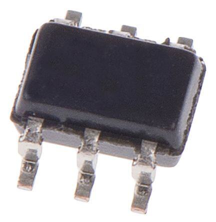
ICGOO电子元器件商城为您提供DAC7311IDCKT由Texas Instruments设计生产,在icgoo商城现货销售,并且可以通过原厂、代理商等渠道进行代购。 DAC7311IDCKT价格参考。Texas InstrumentsDAC7311IDCKT封装/规格:数据采集 - 数模转换器, 12 位 数模转换器 1 SC-70-6。您可以下载DAC7311IDCKT参考资料、Datasheet数据手册功能说明书,资料中有DAC7311IDCKT 详细功能的应用电路图电压和使用方法及教程。
DAC7311IDCKT 是由 Texas Instruments(德州仪器)生产的一款 12 位电压输出数模转换器(DAC)。它属于数据采集系统中的数模转换器类别,广泛应用于需要将数字信号转换为模拟信号的场景。以下是 DAC7311IDCKT 的主要应用场景:

 1. 工业自动化与控制
   - 过程控制:用于调节和控制工业设备中的压力、温度、流量等参数。例如,在自动化生产线中,DAC7311 可以将数字控制信号转换为模拟电压,驱动阀门或电机。
   - 可编程逻辑控制器 (PLC):作为 PLC 的一部分,用于生成精确的模拟输出信号,以实现对机械设备的实时控制。

 2. 仪器仪表
   - 数据采集系统:在测量仪器中,DAC7311 可以生成标准的模拟电压信号,用于校准传感器或测试设备。
   - 信号发生器:用于生成精确的波形信号,如正弦波、方波等,适用于实验室或研发环境。

 3. 通信系统
   - 信号调制与解调:在通信设备中,DAC7311 能够将数字基带信号转换为模拟射频信号,用于传输或接收数据。
   - 音频处理:在低速音频应用中,可以将数字音频信号转换为模拟信号,供扬声器或其他音频设备使用。

 4. 消费电子
   - 家用电器控制:例如,在智能空调或冰箱中,DAC7311 可以将微控制器的数字输出转换为模拟信号,用于控制风扇速度或制冷功率。
   - 医疗设备:在便携式医疗设备(如血压计或血糖仪)中,用于生成稳定的参考电压或驱动传感器。

 5. 汽车电子
   - 车载控制系统:用于调节车灯亮度、座椅加热等功能,通过将数字信号转换为模拟信号来控制执行器。
   - 传感器接口:在汽车传感器系统中,DAC7311 可以为传感器提供精确的偏置电压。

 6. 电源管理
   - 电压调节:在电源管理系统中,DAC7311 可以动态调整输出电压,以适应不同负载的需求。
   - 电池管理:用于监控和调节电池充电/放电过程中的电压水平。

 特点总结
DAC7311IDCKT 具有低功耗、小封装和高精度的特点,适合需要紧凑设计和高效能的应用场合。其单通道设计和灵活的供电范围(2.7V 至 5.5V),使其能够适应多种工作环境。此外,该器件支持 SPI 和兼容的串行接口,便于与微控制器或 FPGA 集成。

总之,DAC7311IDCKT 在需要高精度和稳定性的数模转换场景中表现出色,是许多现代电子系统的核心组件之一。
| 参数 | 数值 |
| 产品目录 | 集成电路 (IC)半导体 |
| 描述 | IC DAC 12-BIT 1-CH LP SC70-6数模转换器- DAC 12B Sgl Ch 80uA DAC |
| 产品分类 | |
| 品牌 | Texas Instruments |
| 产品手册 | http://www.ti.com/litv/sbas442b |
| 产品图片 |
|
| rohs | 符合RoHS无铅 / 符合限制有害物质指令(RoHS)规范要求 |
| 产品系列 | 数据转换器IC,数模转换器- DAC,Texas Instruments DAC7311IDCKT- |
| 数据手册 | |
| 产品型号 | DAC7311IDCKT |
| PCN设计/规格 | |
| 产品目录页面 | |
| 产品种类 | 数模转换器- DAC |
| 位数 | 12 |
| 供应商器件封装 | SC-70-6 |
| 其它名称 | 296-26043-1 |
| 分辨率 | 12 bit |
| 制造商产品页 | http://www.ti.com/general/docs/suppproductinfo.tsp?distId=10&orderablePartNumber=DAC7311IDCKT |
| 包装 | 剪切带 (CT) |
| 商标 | Texas Instruments |
| 安装类型 | 表面贴装 |
| 安装风格 | SMD/SMT |
| 封装 | Reel |
| 封装/外壳 | 6-TSSOP,SC-88,SOT-363 |
| 封装/箱体 | SC-70-6 |
| 工作温度 | -40°C ~ 125°C |
| 工厂包装数量 | 250 |
| 建立时间 | 12µs |
| 接口类型 | Serial (3-Wire, Microwire, QSPI, SPI) |
| 数据接口 | MICROWIRE™,QSPI™,串行,SPI™ |
| 最大功率耗散 | 0.88 mW |
| 最大工作温度 | + 125 C |
| 最小工作温度 | - 40 C |
| 标准包装 | 1 |
| 电压参考 | Supply |
| 电压源 | 单电源 |
| 电源电压-最大 | 5.5 V |
| 电源电压-最小 | 2 V |
| 积分非线性 | +/- 1 LSB |
| 稳定时间 | 10 us |
| 系列 | DAC7311 |
| 结构 | Resistor-String |
| 转换器数 | 1 |
| 转换器数量 | 1 |
| 输出数和类型 | 1 电压,双极 |
| 输出类型 | Voltage Buffered |
| 采样比 | 225 kSPs |
| 采样率(每秒) | - |


- 商务部:美国ITC正式对集成电路等产品启动337调查
- 曝三星4nm工艺存在良率问题 高通将骁龙8 Gen1或转产台积电
- 太阳诱电将投资9.5亿元在常州建新厂生产MLCC 预计2023年完工
- 英特尔发布欧洲新工厂建设计划 深化IDM 2.0 战略
- 台积电先进制程称霸业界 有大客户加持明年业绩稳了
- 达到5530亿美元!SIA预计今年全球半导体销售额将创下新高
- 英特尔拟将自动驾驶子公司Mobileye上市 估值或超500亿美元
- 三星加码芯片和SET,合并消费电子和移动部门,撤换高东真等 CEO
- 三星电子宣布重大人事变动 还合并消费电子和移动部门
- 海关总署:前11个月进口集成电路产品价值2.52万亿元 增长14.8%


PDF Datasheet 数据手册内容提取
Product Sample & Technical Tools & Support & Reference Folder Buy Documents Software Community Design DAC5311,DAC6311,DAC7311 SBAS442C–AUGUST2008–REVISEDJULY2015 DACx311 2-V to 5.5-V, 80-µA, 8-, 10-, and 12-Bit, Low-Power, Single-Channel, Digital-to-Analog Converters in SC70 Package 1 Features 3 Description • RelativeAccuracy: The DAC5311 (8-bit), DAC6311 (10-bit), and 1 DAC7311 (12-bit) devices are low-power, single- – 0.25LSBINL(DAC5311:8-Bit) channel, voltage output digital-to-analog converters – 0.5LSBINL(DAC6311:10-Bit) (DACs).Thelowpowerconsumptionofthesedevices – 1LSBINL(DAC7311:12-Bit) in normal operation (0.55 mW at 5 V, reducing to 2.5 μW in power-down mode) makes it ideally suited for • microPowerOperation:80μAat2.0V portable,battery-operatedapplications. • Power-Down:0.5 μAat5V,0.1 μAat2.0V These devices are monotonic by design, provide • WidePowerSupply:2.0Vto5.5V excellent linearity, and minimize undesired code-to- • Power-OnResettoZeroScale code transient voltages while offering an easy • StraightBinaryDataFormat upgrade path within a pin-compatible family. All devicesuseaversatile,three-wireserialinterfacethat • LowPowerSerialInterfaceWithSchmitt- operates at clock rates of up to 50 MHz and is TriggeredInputs:upto50MHz compatible with standard SPI™, QSPI™, Microwire, • On-ChipOutputBufferAmplifier,Rail-to-Rail anddigitalsignalprocessor(DSP)interfaces. Operation All devices use an external power supply as a • SYNCInterruptFacility reference voltage to set the output range. The • ExtendedTemperatureRange–40°Cto+125°C devices incorporate a power-on reset (POR) circuit • Pin-CompatibleFamilyinaTiny,6-PinSC70 that ensures the DAC output powers up at 0 V and remains there until a valid write to the device occurs. Package The DAC5311, DAC6311, and DAC7311 contain a power-down feature, accessed over the serial 2 Applications interface, that reduces current consumption of the • Portable,Battery-Poweredinstruments deviceto0.1μAat2.0Vinpower-downmode. • ProcessControls These devices are pin-compatible with the DAC8311 • DigitalGainandOffsetAdjustment and DAC8411, offering an easy upgrade path from 8-, 10-, and 12-bit resolution to 14- and 16-bit. All • ProgrammableVoltageandCurrentSources devices are available in a small, 6-pin, SC70 (SOT) package. This package offers a flexible, pin- and SimplifiedSchematic function-compatible, drop-in solution within the family AVDD GND over an extended temperature range of –40°C to +125°C. Power-On Reset DeviceInformation(1) REF(+) PARTNUMBER PACKAGE BODYSIZE(NOM) ReDgAisCter 8-/10-/12-Bit OBuutfpfeurt VOUT DACx311 SC70(6) 2.00mm×1.25mm DAC (1) Forallavailablepackages,seethepackageoptionaddendum attheendofthedatasheet. Input Control Power-Down Logic Control Logic Resistor Network SYNC SCLK D IN 1 An IMPORTANT NOTICE at the end of this data sheet addresses availability, warranty, changes, use in safety-critical applications, intellectualpropertymattersandotherimportantdisclaimers.PRODUCTIONDATA.
DAC5311,DAC6311,DAC7311 SBAS442C–AUGUST2008–REVISEDJULY2015 www.ti.com Table of Contents 1 Features.................................................................. 1 8.3 FeatureDescription.................................................22 2 Applications........................................................... 1 8.4 DeviceFunctionalModes........................................24 3 Description............................................................. 1 8.5 Programming...........................................................25 4 RevisionHistory..................................................... 2 9 ApplicationandImplementation........................ 26 9.1 ApplicationInformation............................................26 5 DeviceComparison............................................... 3 9.2 TypicalApplications ...............................................27 6 PinConfigurationandFunctions......................... 3 10 PowerSupplyRecommendations..................... 30 7 Specifications......................................................... 4 11 Layout................................................................... 31 7.1 AbsoluteMaximumRatings......................................4 11.1 LayoutGuidelines.................................................31 7.2 ESDRatings..............................................................4 11.2 LayoutExample....................................................31 7.3 RecommendedOperatingConditions.......................4 12 DeviceandDocumentationSupport................. 32 7.4 ThermalInformation..................................................4 7.5 ElectricalCharacteristics...........................................5 12.1 RelatedLinks........................................................32 7.6 TimingRequirements................................................7 12.2 CommunityResources..........................................32 7.7 TypicalCharacteristics..............................................8 12.3 Trademarks...........................................................32 12.4 ElectrostaticDischargeCaution............................32 8 DetailedDescription............................................ 22 12.5 Glossary................................................................32 8.1 Overview.................................................................22 13 Mechanical,Packaging,andOrderable 8.2 FunctionalBlockDiagram.......................................22 Information........................................................... 32 4 Revision History NOTE:Pagenumbersforpreviousrevisionsmaydifferfrompagenumbersinthecurrentversion. ChangesfromRevisionB(May2013)toRevisionC Page • AddedESDRatingstable,FeatureDescriptionsection,DeviceFunctionalModes,ApplicationandImplementation section,PowerSupplyRecommendationssection,Layoutsection,DeviceandDocumentationSupportsection,and Mechanical,Packaging,andOrderableInformationsection ................................................................................................. 1 • AddedDeviceComparisonsectionandmovedexistingtablestothisnewsection............................................................... 3 • MovedOperatingTemperatureparameterfromElectricalCharacteristicstabletoRecommendedOperating Conditionstable ..................................................................................................................................................................... 4 • DeletedParameterDefinitionssection;definitionsmovedtonewGlossarysection............................................................ 32 ChangesfromRevisionA(August2011)toRevisionB Page • Changedall1.8Vto2.0Vthroughoutdatasheet................................................................................................................. 1 • Deletedthe1.8-VTypicalCharacteristicssection.................................................................................................................. 8 • ChangedX-axisforFigure36............................................................................................................................................... 12 • ChangedX-axisforFigure37............................................................................................................................................... 12 ChangesfromOriginal(August,2008)toRevisionA Page • Changedspecificationsandtestconditionsforinputlowvoltageparameter......................................................................... 6 • Changedspecificationsandtestconditionsforinputhighvoltageparameter....................................................................... 6 2 SubmitDocumentationFeedback Copyright©2008–2015,TexasInstrumentsIncorporated ProductFolderLinks:DAC5311 DAC6311 DAC7311
DAC5311,DAC6311,DAC7311 www.ti.com SBAS442C–AUGUST2008–REVISEDJULY2015 5 Device Comparison Table1.RelatedDevices RELATEDDEVICES 16-BIT 14-BIT 12-BIT 10-BIT 8-BIT PinandFunctionCompatible DAC8411 DAC8311 DAC7311 DAC6311 DAC5311 Table2.RelativeAccuracyandDifferentialNonlinearity MAXIMUM MAXIMUM RELATIVE DIFFERENTIAL ACCURACY NONLINEARITY DEVICE (LSB) (LSB) DAC5311 ±0.25 ±0.25 DAC6311 ±0.5 ±0.5 DAC7311 ±1 ±1 6 Pin Configuration and Functions DCKPackage 6-PinSC70 TopView SYNC 1 6 V OUT SCLK 2 5 GND D 3 4 AV /V IN DD REF PinFunctions PIN I/O DESCRIPTION NAME NO. AV /V 4 I Powersupplyinput,+2.0Vto+5.5V. DD REF SerialDataInput.Dataareclockedintothe16-bitinputshiftregisteronthefallingedgeofthe D 3 I IN serialclockinput. GND 5 — Groundreferencepointforallcircuitryonthepart. SCLK 2 I Serialclockinput.Dataaretransferredatratesupto50MHz. Level-triggeredcontrolinput(activelow).Thisistheframesychronizationsignalfortheinputdata. WhenSYNCgoeslow,itenablestheinputshiftregisteranddataaretransferredinonthefalling SYNC 1 I edgesofthefollowingclocks.TheDACisupdatedfollowing16thclockcycle,unlessSYNCis takenhighbeforethisedge,inwhichcasetherisingedgeofSYNCactsasaninterruptandthe writesequenceisignoredbytheDACx311.SeetheSYNCInterruptsectionformoredetails. V 6 O AnalogoutputvoltagefromDAC.Theoutputamplifierhasrail-to-railoperation. OUT Copyright©2008–2015,TexasInstrumentsIncorporated SubmitDocumentationFeedback 3 ProductFolderLinks:DAC5311 DAC6311 DAC7311
DAC5311,DAC6311,DAC7311 SBAS442C–AUGUST2008–REVISEDJULY2015 www.ti.com 7 Specifications 7.1 Absolute Maximum Ratings overoperatingfree-airtemperaturerange(unlessotherwisenoted) (1) MIN MAX UNIT AV toGND –0.3 +6 V DD Voltage DigitalinputvoltagetoGND –0.3 +AV +0.3 V DD V toGND –0.3 +AV +0.3 V OUT DD Junction,T max 150 °C J Temperature Storage,T –65 150 °C stg (1) StressesbeyondthoselistedunderAbsoluteMaximumRatingsmaycausepermanentdamagetothedevice.Thesearestressratings only,whichdonotimplyfunctionaloperationofthedeviceattheseoranyotherconditionsbeyondthoseindicatedunderRecommended OperatingConditions.Exposuretoabsolute-maximum-ratedconditionsforextendedperiodsmayaffectdevicereliability. 7.2 ESD Ratings VALUE UNIT Electrostatic Human-bodymodel(HBM),perANSI/ESDA/JEDECJS-001(1) ±1000 V V (ESD) discharge Charged-devicemodel(CDM),perJEDECspecificationJESD22-C101(2) ±500 (1) JEDECdocumentJEP155statesthat500-VHBMallowssafemanufacturingwithastandardESDcontrolprocess. (2) JEDECdocumentJEP157statesthat250-VCDMallowssafemanufacturingwithastandardESDcontrolprocess. 7.3 Recommended Operating Conditions overoperatingfree-airtemperaturerange(unlessotherwisenoted) MIN NOM MAX UNIT T Operatingtemperature –40 125 °C A AV Supplyvoltage 2 5.5 V DD 7.4 Thermal Information DACx311 THERMALMETRIC(1) DCK(SC70) UNIT 6PINS R Junction-to-ambientthermalresistance 216.4 °C/W θJA R Junction-to-case(top)thermalresistance 52.1 °C/W θJC(top) R Junction-to-boardthermalresistance 65.9 °C/W θJB ψ Junction-to-topcharacterizationparameter 1.3 °C/W JT ψ Junction-to-boardcharacterizationparameter 65.2 °C/W JB R Junction-to-case(bottom)thermalresistance N/A °C/W θJC(bot) (1) Formoreinformationabouttraditionalandnewthermalmetrics,seetheSemiconductorandICPackageThermalMetricsapplication report,SPRA953. 4 SubmitDocumentationFeedback Copyright©2008–2015,TexasInstrumentsIncorporated ProductFolderLinks:DAC5311 DAC6311 DAC7311
DAC5311,DAC6311,DAC7311 www.ti.com SBAS442C–AUGUST2008–REVISEDJULY2015 7.5 Electrical Characteristics atAV =2.0Vto5.5V,R =2kΩtoGND,C =200pFtoGND,andT =–40°Cto+125°C(unlessotherwisenoted) DD L L A PARAMETER TESTCONDITIONS MIN TYP MAX UNIT STATICPERFORMANCE(1) DAC5311 8 Bits DAC6311 Resolution 10 Bits DAC7311 12 Bits Measuredbythelinepassingthrough DAC5311 ±0.01 ±0.25 LSB codes3and252 Measuredbythelinepassingthrough DAC6311 Relativeaccuracy ±0.06 ±0.5 LSB codes12and1012 Measuredbythelinepassingthrough DAC7311 ±0.3 ±1 LSB codes30and4050 DAC5311 ±0.01 ±0.25 LSB Differential DAC6311 ±0.03 ±0.5 LSB nonlinearity DAC7311 ±0.2 ±1 LSB Measuredbythelinepassingthroughtwo Offseterror codes(2) ±0.05 ±4 mV Offseterrordrift 3 μV/°C Zerocodeerror AllzerosloadedtotheDACregister 0.2 mV %of Full-scaleerror AllonesloadedtoDACregister 0.04 0.2 FSR %of Gainerror 0.05 ±0.15 FSR AVDD=5V ±0.5 ppmof Gaintemperaturecoefficient AV =2.0V ±1.5 FSR/°C DD OUTPUTCHARACTERISTICS Outputvoltagerange 0 AV V DD R =2kΩ,C =200pF,AV =5V, L L DD 6 10 μs Outputvoltagesettlingtime(3) 1/4scaleto3/4scale R =2MΩ,C =470pF 12 μs L L Slewrate 0.7 V/μs R =∞ 470 pF L Capacitiveloadstability R =2kΩ 1000 pF L Codechangeglitchimpulse 1LSBchangearoundmajorcarry 0.5 nV-s Digitalfeedthrough 0.5 nV-s Power-onglitchimpulse R =2kΩ,C =200pF,AV =5V 17 mV L L DD DCoutputimpedance 0.5 Ω AV =5V 50 mA DD Shortcircuitcurrent AV =3V 20 mA DD Power-uptime Comingoutofpower-downmode 50 μs (1) Linearitycalculatedusingareducedcoderangeof3to252for8-bit,12to1012for10bit,and30to4050for12-bit,outputunloaded. (2) Straightlinepassingthroughcodes3and252for8-bit,12and1012for10-bit,and30and4050for12-bit,outputunloaded. (3) Specifiedbydesignandcharacterization,notproductiontested. Copyright©2008–2015,TexasInstrumentsIncorporated SubmitDocumentationFeedback 5 ProductFolderLinks:DAC5311 DAC6311 DAC7311
DAC5311,DAC6311,DAC7311 SBAS442C–AUGUST2008–REVISEDJULY2015 www.ti.com Electrical Characteristics (continued) atAV =2.0Vto5.5V,R =2kΩtoGND,C =200pFtoGND,andT =–40°Cto+125°C(unlessotherwisenoted) DD L L A PARAMETER TESTCONDITIONS MIN TYP MAX UNIT ACPERFORMANCE SNR 81 dB T =+25°C,BW=20kHz,12-bitlevel, A THD AV =5V, –65 dB DD SFDR fOUT=1kHz,1st19harmonicsremovedfor 65 dB SNRcalculation SINAD 65 dB T =+25°C,atzero-scaleinput, A 17 nV/√Hz f =1kHz,AV =5V DACoutputnoisedensity(4) OUT DD T =+25°C,atmid-codeinput, A 110 nV/√Hz f =1kHz,AV =5V OUT DD DACoutputnoise(5) TA=+25°C,atmid-codeinput, 3 μV 0.1Hzto10Hz,AV =5V PP DD LOGICINPUTS(6) Inputcurrent ±1 μA AV =2.7Vto5.5V 0.3×AV V DD DD V L,Inputlowvoltage IN AV =2.0Vto2.7V 0.1×AV V DD DD AV =2.7Vto5.5V 0.7×AV V DD DD V H,Inputhighvoltage IN AV =2.0Vto2.7V 0.9×AV V DD DD Pincapacitance 1.5 3 pF POWERREQUIREMENTS AV 2.0 5.5 V DD AV =3.6Vto5.5V 110 160 μA V H=AV and DD IN DD Normalmode V L=GND,at AV =2.7Vto3.6V 95 150 μA IN DD midscalecode(7) AV =2.0Vto2.7V 80 140 μA DD I DD AV =3.6Vto5.5V 0.5 3.5 μA V H=AV and DD IN DD Allpower-downmode V L=GND,at AV =2.7Vto3.6V 0.4 3 μA IN DD midscalecode(7) AV =2.0Vto2.7V 0.1 2 μA DD AV =3.6Vto5.5V 0.55 0.88 mW V H=AV and DD IN DD Normalmode V L=GND,at AV =2.7Vto3.6V 0.25 0.54 mW IN DD midscalecode(7) AV =2.0Vto2.7V 0.14 0.38 mW DD Powerdissipation AV =3.6Vto5.5V 2.50 19.2 µW V H=AV and DD IN DD Allpower-downmode V L=GND,at AV =2.7Vto3.6V 1.08 10.8 µW IN DD midscalecode(7) AV =2.0Vto2.7V 0.72 8.1 µW DD (4) Formoredetails,seeFigure23. (5) Formoredetails,seeFigure24. (6) Specifiedbydesignandcharacterization,notproductiontested. (7) Formoredetails,seeFigure16andFigure58. 6 SubmitDocumentationFeedback Copyright©2008–2015,TexasInstrumentsIncorporated ProductFolderLinks:DAC5311 DAC6311 DAC7311
DAC5311,DAC6311,DAC7311 www.ti.com SBAS442C–AUGUST2008–REVISEDJULY2015 7.6 Timing Requirements at–40°Cto125°C,andAV =2Vto5.5V(unlessotherwisenoted)(1) DD MIN NOM MAX UNIT AV =2.0Vto3.6V 20 DD f Serialclockfrequency MHz (SCLK) AV =3.6Vto5.5V 50 DD AV =2.0Vto3.6V 50 DD t SCLKcycletime ns 1 AV =3.6Vto5.5V 20 DD AV =2.0Vto3.6V 25 DD t SCLKhightime ns 2 AV =3.6Vto5.5V 10 DD AV =2.0Vto3.6V 25 DD t SCLKlowtime ns 3 AV =3.6Vto5.5V 10 DD AV =2.0Vto3.6V 0 DD t SYNCtoSCLKrisingedgesetuptime ns 4 AV =3.6Vto5.5V 0 DD AV =2.0Vto3.6V 5 DD t Datasetuptime ns 5 AV =3.6Vto5.5V 5 DD AV =2.0Vto3.6V 4.5 DD t Dataholdtime ns 6 AV =3.6Vto5.5V 4.5 DD AV =2.0Vto3.6V 0 DD t SCLKfallingedgetoSYNCrisingedge ns 7 AV =3.6Vto5.5V 0 DD AV =2.0Vto3.6V 50 DD t MinimumSYNChightime ns 8 AV =3.6Vto5.5V 20 DD AV =2.0Vto3.6V 100 DD t 16thSCLKfallingedgetoSYNCfallingedge ns 9 AV =3.6Vto5.5V 100 DD SYNCrisingedgeto16thSCLKfallingedge AVDD=2.0Vto3.6V 15 t ns 10 (forsuccessfulSYNCinterrupt) AV =3.6Vto5.5V 15 DD (1) Allinputsignalsarespecifiedwitht =t =3ns(10%to90%ofAV )andtimedfromavoltagelevelof(V +V )/2. R F DD IL IH t t 1 9 SCLK 1 16 t8 t t3 t2 t7 4 SYNC t t 10 6 t 5 D DB15 DB0 DB15 IN Figure1. SerialWriteOperation Copyright©2008–2015,TexasInstrumentsIncorporated SubmitDocumentationFeedback 7 ProductFolderLinks:DAC5311 DAC6311 DAC7311
DAC5311,DAC6311,DAC7311 SBAS442C–AUGUST2008–REVISEDJULY2015 www.ti.com 7.7 Typical Characteristics 7.7.1 TypicalCharacteristics:AV =5V DD atT =25°C,AV =5V,andDACloadedwithmidscalecode(unlessotherwisenoted) A DD 0.50 0.10 AV = 5V AV = 5V DD DD B) 0.25 B) 0.05 S S L 0 L 0 E ( E ( L-0.25 L-0.05 -0.50 -0.10 0.2 0.06 B) 0.1 B) 0.03 S S E (L 0 E (L 0 DL -0.1 DL-0.03 -0.2 -0.06 0 512 1024 1536 2048 2560 3072 3584 4096 0 128 256 384 512 640 768 896 1024 Digital Input Code Digital Input Code Figure2. DAC731112-BitLinearityErrorandDifferential Figure3. DAC631110-BitLinearityErrorandDifferential LinearityErrorvsCode(–40°C) LinearityErrorvsCode(–40°C) 0.50 0.10 AV = 5V AV = 5V DD DD B) 0.25 B) 0.05 S S L 0 L 0 E ( E ( L-0.25 L-0.05 -0.50 -0.10 0.2 0.06 B) 0.1 B) 0.03 S S E (L 0 E (L 0 DL -0.1 DL-0.03 -0.2 -0.06 0 512 1024 1536 2048 2560 3072 3584 4096 0 128 256 384 512 640 768 896 1024 Digital Input Code Digital Input Code Figure4. DAC731112-BitLinearityErrorandDifferential Figure5. DAC631110-BitLinearityErrorandDifferential LinearityErrorvsCode(25°C) LinearityErrorvsCode(25°C) 0.50 0.10 AV = 5V AV = 5V DD DD B) 0.25 B) 0.05 S S L 0 L 0 E ( E ( L-0.25 L-0.05 -0.50 -0.10 0.2 0.06 B) 0.1 B) 0.03 S S E (L 0 E (L 0 DL -0.1 DL-0.03 -0.2 -0.06 0 512 1024 1536 2048 2560 3072 3584 4096 0 128 256 384 512 640 768 896 1024 Digital Input Code Digital Input Code Figure6. DAC731112-BitLinearityErrorandDifferential Figure7. DAC631110-BitLinearityErrorandDifferential LinearityErrorvsCode(125°C) LinearityErrorvsCode(125°C) 8 SubmitDocumentationFeedback Copyright©2008–2015,TexasInstrumentsIncorporated ProductFolderLinks:DAC5311 DAC6311 DAC7311
DAC5311,DAC6311,DAC7311 www.ti.com SBAS442C–AUGUST2008–REVISEDJULY2015 Typical Characteristics: AV = 5 V (continued) DD atT =25°C,AV =5V,andDACloadedwithmidscalecode(unlessotherwisenoted) A DD 0.02 0.4 B) 0.01 AVDD= 5V AVDD= 5V S L 0 LE (--00..0012 e Error (mV) 00..32 0.02 d o C B) 0.01 o- E (LS 0 Zer 0.1 DL-0.01 -0.02 0 0 32 64 96 128 160 192 224 256 -40 -25 -10 5 20 35 50 65 80 95 110 125 Digital Input Code Temperature (°C) Figure8. DAC53118-BitLinearityErrorandDifferential Figure9.Zero-CodeErrorvsTemperature LinearityErrorvsCode(–40°C) 0.02 0.6 SB) 0.01 AVDD= 5V 0.4 AVDD= 5V L 0 E ( L-0.01 V) 0.2 m -0.02 or ( 0.02 et Err 0 B) 0.01 Offs -0.2 S E (L 0 -0.4 DL-0.01 -0.02 -0.6 0 32 64 96 128 160 192 224 256 -40 -25 -10 5 20 35 50 65 80 95 110 125 Digital Input Code Temperature (°C) Figure10. DAC53118-BitLinearityErrorandDifferential Figure11.OffsetErrorvsTemperature LinearityErrorvsCode(25°C) 0.02 0.06 SB) 0.01 AVDD= 5V 0.04 AVDD= 5V L 0 E ( V) L-0.01 m 0.02 -0.02 Error ( 0 0.02 ale c SB) 0.01 ull-S -0.02 E (L 0 F -0.04 DL-0.01 -0.02 -0.06 0 32 64 96 128 160 192 224 256 -40 -25 -10 5 20 35 50 65 80 95 110 125 Digital Input Code Temperature (°C) Figure12. DAC53118-BitLinearityErrorandDifferential Figure13.Full-ScaleErrorvsTemperature LinearityErrorvsCode(125°C) Copyright©2008–2015,TexasInstrumentsIncorporated SubmitDocumentationFeedback 9 ProductFolderLinks:DAC5311 DAC6311 DAC7311
DAC5311,DAC6311,DAC7311 SBAS442C–AUGUST2008–REVISEDJULY2015 www.ti.com Typical Characteristics: AV = 5 V (continued) DD atT =25°C,AV =5V,andDACloadedwithmidscalecode(unlessotherwisenoted) A DD 5.5 0.6 AV = 5V DD DAC Loaded with 000h 5.0 V) V) e ( e ( ag 4.5 ag 0.4 olt olt V V ut 4.0 ut p p ut ut O O g 3.5 g 0.2 o o al al n n A 3.0 A AV = 5V DD DAC Loaded with FFFh 2.5 0 0 2 4 6 8 10 0 2 4 6 8 10 I (mA) I (mA) SOURCE SINK Figure14.SourceCurrentatPositiveRail Figure15.SinkCurrentatNegativeRail 120 2000 AV = 5.5V SYNC Input (all other digital inputs = GND) DD A) A) m m 1500 nt ( 100 nt ( Sweep from e e urr urr 0V to 5.5V C C y y 1000 pl pl up up Sweep from er-S 80 er-S 5.5V to 0V w w 500 o o P P 60 0 0 512 1024 1536 2048 2560 3072 3584 4096 0 0.5 1.0 1.5 2.0 2.5 3.0 3.5 4.0 4.5 5.0 Digital Input Code VLOGIC(V) Figure16.Power-SupplyCurrentvsDigitalInputCode Figure17.Power-SupplyCurrentvsLogicInputVoltage 140 1.6 AV = 5V AV = 5V DD DD A) my Current ( 113200 Current (mA) 10..28 ower-Suppl 110 Quiescent 0.4 P 100 0 -40 -25 -10 5 20 35 50 65 80 95 110 125 -40 -25 -10 5 20 35 50 65 80 95 110 125 Temperature (°C) Temperature (°C) Figure18.Power-SupplyCurrentvsTemperature Figure19.Power-DownCurrentvsTemperature 10 SubmitDocumentationFeedback Copyright©2008–2015,TexasInstrumentsIncorporated ProductFolderLinks:DAC5311 DAC6311 DAC7311
DAC5311,DAC6311,DAC7311 www.ti.com SBAS442C–AUGUST2008–REVISEDJULY2015 Typical Characteristics: AV = 5 V (continued) DD atT =25°C,AV =5V,andDACloadedwithmidscalecode(unlessotherwisenoted) A DD -20 102 AV = 5V, f = 225kSPS, AV = 5V, f = 225kSPS, DD S DD S -1dB FSR Digital Input, -1dB FSR Digital Input, Measurement Bandwidth = 20kHz Measurement Bandwidth = 20kHz -40 94 THD B) B) D (d -60 R (d 86 H N T S 2nd Harmonic -80 78 3rd Harmonic -100 70 0 1 2 3 4 5 0 1 2 3 4 5 f (kHz) f (kHz) OUT OUT Figure20.TotalHarmonicDistortionvsOutputFrequency Figure21.Signal-to-NoiseRatiovsOutputFrequency 0 300 AVDD= 5V, AVDD= 5V 20 fOUT= 1kHz, fS= 225kSPS, 250 Measurement Bandwidth = 20kHz -40 )z 200 B) -60 ÖH ain (d -80 e (nV/ 150 Midscale G s Noi 100 -100 Full Scale Zero Scale -120 50 -140 0 0 5 10 15 20 10 100 1k 10k 100k Frequency (kHz) Frequency (Hz) Figure22.PowerSpectralDensity Figure23.DACOutputNoiseDensityvsFrequency AV = 5V, DD DAC = Midscale, No Load V/div) V/div) (1mSE m(500 VNOI VOUT 3mV PP AV = 5V DD Clock Feedthrough Impulse ~0.5nV-s Time (2s/div) Time (500ns/div) Figure24.DACOutputNoise,0.1-Hzto10-HzBandwidth Figure25.ClockFeedthrough,5-V,2-MHz,Midscale Copyright©2008–2015,TexasInstrumentsIncorporated SubmitDocumentationFeedback 11 ProductFolderLinks:DAC5311 DAC6311 DAC7311
DAC5311,DAC6311,DAC7311 SBAS442C–AUGUST2008–REVISEDJULY2015 www.ti.com Typical Characteristics: AV = 5 V (continued) DD atT =25°C,AV =5V,andDACloadedwithmidscalecode(unlessotherwisenoted) A DD AV = 5V DD From Code: 800h AV = 5V DD To Code: 801h From Code: 801h v) v) To Code: 800h di di V/ V/ m m 0 0 0 0 5 5 ( ( UT Glitch Impulse UT VO < 0.5nV-s VO Clock Clock Feedthrough Feedthrough ~0.5nV-s ~0.5nV-s Glitch Impulse < 0.5nV-s Time (5ms/div) Time (5ms/div) Figure26.GlitchEnergy,5-V,12-Bit,1-LSBStep,Rising Figure27.GlitchEnergy,5-V,12-Bit,1-LSBStep,Falling Edge Edge Glitch Impulse ~1nV-s AV = 5V DD From Code: 81h v) v) To Code: 80h di di V/ V/ m m 5 5 ( ( UT UT Clock Glitch Impulse O O ~1nV-s V V Feedthrough ~0.5nV-s Clock AV = 5V DD Feedthrough From Code: 80h ~0.5nV-s To Code: 81h Time (5ms/div) Time (5ms/div) Figure28.GlitchEnergy,5-V,8-Bit,1-LSBStep,Rising Figure29.GlitchEnergy,5-V,8-Bit,1-LSBStep,Falling Edge Edge AV = 5V AV = 5V DD DD From Code: 000h From Code: FFFh To Code: FFFh To Code: 000h Rising Edge 1V/div Zoomed Rising Edge Falling Edge Zoomed Falling Edge 100mV/div 1V/div 100mV/div Trigger Pulse 5V/div Trigger Pulse 5V/div Time (2ms/div) Time (2ms/div) Figure30.Full-ScaleSettlingTime,5-VRisingEdge Figure31.Full-ScaleSettlingTime,5-VFallingEdge 12 SubmitDocumentationFeedback Copyright©2008–2015,TexasInstrumentsIncorporated ProductFolderLinks:DAC5311 DAC6311 DAC7311
DAC5311,DAC6311,DAC7311 www.ti.com SBAS442C–AUGUST2008–REVISEDJULY2015 Typical Characteristics: AV = 5 V (continued) DD atT =25°C,AV =5V,andDACloadedwithmidscalecode(unlessotherwisenoted) A DD Falling AV = 5V DD Edge From Code: C00h 1V/div To Code: 400h Rising Edge Zoomed Rising Edge Zoomed Falling Edge 1V/div 100mV/div 100mV/div Trigger AVDD= 5V Trigger Pulse From Code: 400h Pulse 5V/div To Code: C00h 5V/div Time (2ms/div) Time (2ms/div) Figure32.Half-ScaleSettlingTime,5-VRisingEdge Figure33.Half-ScaleSettlingTime5-VFallingEdge AV = 5V v) v) DAC = ZerDoD Scale V/di V/di Load = 200pF || 10kW 2 2 ( ( D D D D V V A AV = 5V A DD DAC = Zero Scale Load = 200pF || 10kW v) 17mV v) di di V/ V/ m m 0 0 2 2 ( ( UT UT O O V V Time (5ms/div) Time (10ms/div) Figure34.Power-OnResetto0-VPower-OnGlitch Figure35.Power-OffGlitch 120 0.4 AV = 2.0V to 5.5V AV = 2.0V to 5.5V DD DD A) 110 y Current (m 100 Current (A)m 00..32 ower-Suppl 9800 Quiescent 0.1 P 70 0 2.0 2.5 3.0 3.5 4.0 4.5 5.0 5.5 2.0 2.5 3.0 3.5 4.0 4.5 5.0 5.5 AV (V) AV (V) DD DD Figure36.Power-SupplyCurrentvsPower-SupplyVoltage Figure37.Power-DownCurrentvsPower-SupplyVoltage Copyright©2008–2015,TexasInstrumentsIncorporated SubmitDocumentationFeedback 13 ProductFolderLinks:DAC5311 DAC6311 DAC7311
DAC5311,DAC6311,DAC7311 SBAS442C–AUGUST2008–REVISEDJULY2015 www.ti.com Typical Characteristics: AV = 5 V (continued) DD atT =25°C,AV =5V,andDACloadedwithmidscalecode(unlessotherwisenoted) A DD 50 AV = 5.5V DD 45 40 35 s e 30 c n urre 25 cc 20 O 15 10 5 0 0 4 8 2 6 0 4 8 2 6 0 4 8 2 6 0 8 8 8 9 9 0 0 0 1 1 2 2 2 3 3 4 1 1 1 1 1 1 1 1 1 1 1 I (mA) DD Figure38.Power-SupplyCurrentHistogram 14 SubmitDocumentationFeedback Copyright©2008–2015,TexasInstrumentsIncorporated ProductFolderLinks:DAC5311 DAC6311 DAC7311
DAC5311,DAC6311,DAC7311 www.ti.com SBAS442C–AUGUST2008–REVISEDJULY2015 7.7.2 TypicalCharacteristics:AV =3.6V DD atT =25°C,AV =3.6V,andDACloadedwithmidscalecode(unlessotherwisenoted) A DD 1.2 1200 AV = 3.6V SYNC Input (all other digital inputs = GND) DD A) mA) 900 urrent (m 0.8 Current ( S0Vw etoe p3 .f6roVm C y 600 scent 0.4 Suppl Quie wer- 300 o P Sweep from 3.6V to 0V 0 0 -40 -25 -10 5 20 35 50 65 80 95 110 125 0 0.5 1.0 1.5 2.0 2.5 3.0 3.5 4.0 Temperature (°C) V (V) LOGIC Figure39.Power-DownCurrentvsTemperature Figure40.Power-SupplyCurrentvsLogicInputVoltage 50 3.7 AV = 3.6V DD 45 3.5 40 V) 35 e ( s ag 3.3 ce 30 olt n V urre 25 put 3.1 cc 20 ut O O 15 g 2.9 o 10 nal A 2.7 5 AV = 3.6V DD 0 DAC Loaded with FFFFh 0 4 8 2 6 0 4 8 2 6 0 4 8 2 6 0 2.5 7 7 7 8 8 9 9 9 10 10 11 11 11 12 12 13 0 2 4 6 8 10 IDD(mA) ISOURCE(mA) Figure41.Power-SupplyCurrentHistogram Figure42.SourceCurrentatPositiveRail 0.6 AV = 3.6V DD DAC Loaded with 0000h V) e ( ag 0.4 olt V ut p ut O g 0.2 o al n A 0 0 2 4 6 8 10 I (mA) SINK Figure43.SinkCurrentatNegativeRail Copyright©2008–2015,TexasInstrumentsIncorporated SubmitDocumentationFeedback 15 ProductFolderLinks:DAC5311 DAC6311 DAC7311
DAC5311,DAC6311,DAC7311 SBAS442C–AUGUST2008–REVISEDJULY2015 www.ti.com 7.7.3 TypicalCharacteristics:AV =2.7V DD atT =25°C,AV =2.7V,andDACloadedwithmidscalecode(unlessotherwisenoted) A DD 0.50 0.10 AV = 2.7V AV = 2.7V DD DD B) 0.25 B) 0.05 S S L 0 L 0 E ( E ( L-0.25 L-0.05 -0.50 -0.10 0.2 0.06 B) 0.1 B) 0.03 S S E (L 0 E (L 0 DL -0.1 DL-0.03 -0.2 -0.06 0 512 1024 1536 2048 2560 3072 3584 4096 0 128 256 384 512 640 768 896 1024 Digital Input Code Digital Input Code Figure44. DAC731112-BitLinearityErrorandDifferential Figure45. DAC631110-BitLinearityErrorandDifferential LinearityErrorvsCode(–40°C) LinearityErrorvsCode(–40°C) 0.50 0.10 AV = 2.7V AV = 2.7V DD DD B) 0.25 B) 0.05 S S L 0 L 0 E ( E ( L-0.25 L-0.05 -0.50 -0.10 0.2 0.06 B) 0.1 B) 0.03 S S E (L 0 E (L 0 DL -0.1 DL-0.03 -0.2 -0.06 0 512 1024 1536 2048 2560 3072 3584 4096 0 128 256 384 512 640 768 896 1024 Digital Input Code Digital Input Code Figure46. DAC731112-BitLinearityErrorandDifferential Figure47. DAC631110-BitLinearityErrorandDifferential LinearityErrorvsCode(25°C) LinearityErrorvsCode(25°C) 0.50 0.10 AV = 2.7V AV = 2.7V DD DD B) 0.25 B) 0.05 S S L 0 L 0 E ( E ( L-0.25 L-0.05 -0.50 -0.10 0.2 0.06 B) 0.1 B) 0.03 S S E (L 0 E (L 0 DL -0.1 DL-0.03 -0.2 -0.06 0 512 1024 1536 2048 2560 3072 3584 4096 0 128 256 384 512 640 768 896 1024 Digital Input Code Digital Input Code Figure48. DAC731112-BitLinearityErrorandDifferential Figure49. DAC631110-BitLinearityErrorandDifferential LinearityErrorvsCode(125°C) LinearityErrorvsCode(125°C) 16 SubmitDocumentationFeedback Copyright©2008–2015,TexasInstrumentsIncorporated ProductFolderLinks:DAC5311 DAC6311 DAC7311
DAC5311,DAC6311,DAC7311 www.ti.com SBAS442C–AUGUST2008–REVISEDJULY2015 Typical Characteristics: AV = 2.7 V (continued) DD atT =25°C,AV =2.7V,andDACloadedwithmidscalecode(unlessotherwisenoted) A DD 0.02 0.4 B) 0.01 AVDD= 2.7V AVDD= 2.7V S L 0 LE (--00..0012 e Error (mV) 00..32 0.02 d o C B) 0.01 o- E (LS 0 Zer 0.1 DL-0.01 -0.02 0 0 32 64 96 128 160 192 224 256 -40 -25 -10 5 20 35 50 65 80 95 110 125 Digital Input Code Temperature (°C) Figure50. DAC53118-BitLinearityErrorandDifferential Figure51.Zero-CodeErrorvsTemperature LinearityErrorvsCode(–40°C) 0.02 0.6 SB) 0.01 AVDD= 2.7V 0.4 AVDD= 2.7V L 0 E ( L-0.01 V) 0.2 m -0.02 or ( 0.02 et Err 0 B) 0.01 Offs -0.2 S E (L 0 -0.4 DL-0.01 -0.02 -0.6 0 32 64 96 128 160 192 224 256 -40 -25 -10 5 20 35 50 65 80 95 110 125 Digital Input Code Temperature (°C) Figure52. DAC53118-BitLinearityErrorandDifferential Figure53.OffsetErrorvsTemperature LinearityErrorvsCode(25°C) 0.02 0.06 SB) 0.01 AVDD= 2.7V 0.04 AVDD= 2.7V L 0 E ( V) L-0.01 m 0.02 -0.02 Error ( 0 0.02 ale c SB) 0.01 ull-S -0.02 E (L 0 F -0.04 DL-0.01 -0.02 -0.06 0 32 64 96 128 160 192 224 256 -40 -25 -10 5 20 35 50 65 80 95 110 125 Digital Input Code Temperature (°C) Figure54. DAC53118-BitLinearityErrorandDifferential Figure55.Full-ScaleErrorvsTemperature LinearityErrorvsCode(125°C) Copyright©2008–2015,TexasInstrumentsIncorporated SubmitDocumentationFeedback 17 ProductFolderLinks:DAC5311 DAC6311 DAC7311
DAC5311,DAC6311,DAC7311 SBAS442C–AUGUST2008–REVISEDJULY2015 www.ti.com Typical Characteristics: AV = 2.7 V (continued) DD atT =25°C,AV =2.7V,andDACloadedwithmidscalecode(unlessotherwisenoted) A DD 2.8 0.6 AV = 2.7V DD DAC Loaded with 000h V) V) e ( 2.6 e ( ag ag 0.4 olt olt V V ut 2.4 ut p p ut ut O O g g 0.2 o o al 2.2 al n n A A AV = 2.7V DD DAC Loaded with FFFh 2.0 0 0 2 4 6 8 10 0 2 4 6 8 10 I (mA) I (mA) SOURCE SINK Figure56.SourceCurrentatPositiveRail Figure57.SinkCurrentatNegativeRail 100 800 AV = 2.7V SYNC Input (all other digital inputs = GND) DD A) 90 A) m m 600 nt ( nt ( Curre 80 Curre S0Vw etoe p2 .f7roVm ply ply 400 up 70 up Sweep from er-S er-S 2.7V to 0V w w 200 Po 60 Po 50 0 0 512 1024 1536 2048 2560 3072 3584 4096 0 0.5 1.0 1.5 2.0 2.5 3.0 Digital Input Code V (V) LOGIC Figure58.Power-SupplyCurrentvsDigitalInputCode Figure59.Power-SupplyCurrentvsLogicInputVoltage 120 1.0 AV = 2.7V AV = 2.7V DD DD A) 110 0.8 mCurrent ( 100 urrent (mA) 0.6 y C Power-Suppl 9800 Quiescent 00..42 70 0 -40 -25 -10 5 20 35 50 65 80 95 110 125 -40 -25 -10 5 20 35 50 65 80 95 110 125 Temperature (°C) Temperature (°C) Figure60.Power-SupplyCurrentvsTemperature Figure61.Power-DownCurrentvsTemperature 18 SubmitDocumentationFeedback Copyright©2008–2015,TexasInstrumentsIncorporated ProductFolderLinks:DAC5311 DAC6311 DAC7311
DAC5311,DAC6311,DAC7311 www.ti.com SBAS442C–AUGUST2008–REVISEDJULY2015 Typical Characteristics: AV = 2.7 V (continued) DD atT =25°C,AV =2.7V,andDACloadedwithmidscalecode(unlessotherwisenoted) A DD -20 94 AV = 2.7V, f = 225kSPS, AV = 2.7V, f = 225kSPS, DD S DD S -1dB FSR Digital Input, -1dB FSR Digital Input, Measurement Bandwidth = 20kHz THD 90 Measurement Bandwidth = 20kHz -40 86 B) B) D (d -60 R (d 82 H N T S 2nd Harmonic 78 -80 74 3rd Harmonic -100 70 0 1 2 3 4 5 0 1 2 3 4 5 f (kHz) f (kHz) OUT OUT Figure62.TotalHarmonicDistortionvsOutputFrequency Figure63.Signal-to-NoiseRatiovsOutputFrequency 0 50 AAVVDDDD== 22..77VV,, 45 AVDD= 2.7V 20 ffOOUUTT== 11kkHHzz,, ffSS== 222255kkSSPPSS,, MMeeaassuurreemmeenntt BBaannddwwiiddtthh == 2200kkHHzz 40 -40 35 s n (dB) -60 urrence 3205 Gai -80 Occ 20 15 -100 10 -120 5 0 -140 0 4 8 2 6 0 4 8 2 6 0 4 6 6 6 7 7 8 8 8 9 9 0 0 0 5 10 15 20 1 1 Frequency (kHz) IDD(mA) Figure65.Power-SupplyCurrentHistogram Figure64.PowerSpectralDensity v) v) di di Glitch Impulse V/ V/ < 0.3nV-s m m 0 0 0 0 5 2 ( ( UT UT O O V V Clock AVDD= 2.7V AV = 2.7V Feedthrough From Code: 800h Clock Feedthrough Impulse D~D0.4nV-s ~0.4nV-s To Code: 801h Time (5ms/div) Time (5ms/div) Figure66.ClockFeedthrough2.7-V,20-MHz,Midscale Figure67.GlitchEnergy,2.7-V,12-Bit,1-LSBStep,Rising Edge Copyright©2008–2015,TexasInstrumentsIncorporated SubmitDocumentationFeedback 19 ProductFolderLinks:DAC5311 DAC6311 DAC7311
DAC5311,DAC6311,DAC7311 SBAS442C–AUGUST2008–REVISEDJULY2015 www.ti.com Typical Characteristics: AV = 2.7 V (continued) DD atT =25°C,AV =2.7V,andDACloadedwithmidscalecode(unlessotherwisenoted) A DD AV = 2.7V DD From Code: 801h m0V/div) To Code: 800h mV/div) G~1lintcVh- sImpulse V(20OUT Clock V(2OUT CF~e0loe.4cdnkthVr-osugh Feedthrough ~0.4nV-s Glitch Impulse AVDD= 2.7V From Code: 80h < 0.3nV-s To Code: 81h Time (5ms/div) Time (5ms/div) Figure68.GlitchEnergy,2.7-V,12-Bit,1-LSBStep,Falling Figure69.GlitchEnergy,2.7-V,8-Bit,1-LSBStep,Rising Edge Edge AV = 2.7V DD From Code: 000h AVDD= 2.7V To Code: FFFh From Code: 81h v) To Code: 80h Rising Edge di V/ 1V/div m 2 ( Zoomed Rising Edge OUT Clock 100mV/div V Feedthrough Glitch Impulse ~0.4nV-s ~1nV-s Trigger Pulse 2.7V/div Time (5ms/div) Time (2ms/div) Figure70.GlitchEnergy,2.7-V,8-Bit,1-LSBStep,Falling Figure71.Full-ScaleSettlingTime,2.7-VRisingEdge Edge AV = 2.7V AV = 2.7V DD DD From Code: FFFh From Code: 400h To Code: 000h To Code: C00h Falling Edge 1V/div Rising Edge Zoomed Falling Edge 1V/div 100mV/div Zoomed Rising Edge 100mV/div Trigger Pulse Trigger Pulse 2.7V/div 2.7V/div Time (2ms/div) Time (2ms/div) Figure72.Full-ScaleSettlingTime,2.7-VFallingEdge Figure73.Half-ScaleSettlingTime,2.7-VRisingEdge 20 SubmitDocumentationFeedback Copyright©2008–2015,TexasInstrumentsIncorporated ProductFolderLinks:DAC5311 DAC6311 DAC7311
DAC5311,DAC6311,DAC7311 www.ti.com SBAS442C–AUGUST2008–REVISEDJULY2015 Typical Characteristics: AV = 2.7 V (continued) DD atT =25°C,AV =2.7V,andDACloadedwithmidscalecode(unlessotherwisenoted) A DD AV = 2.7V FroDmD Code: C00h div) To Code: 400h V/ 1 Falling (D Edge VD A AV = 2.7V 1V/div DD DAC = Zero Scale Load = 200pF || 10kW v) 17mV di Trigger V/ m Pulse 0 2 2.7V/div Zoomed Falling Edge (UT 100mV/div O V Time (2ms/div) Time (5ms/div) Figure74.Half-ScaleSettlingTime,2.7-VFallingEdge Figure75.Power-OnResetto0-VPower-OnGlitch AV = 2.7V v) DAC = ZDeDro Scale V/di Load = 200pF || 10kW 1 ( D D V A v) di V/ m 0 2 ( UT O V Time (10ms/div) Figure76.Power-OffGlitch Copyright©2008–2015,TexasInstrumentsIncorporated SubmitDocumentationFeedback 21 ProductFolderLinks:DAC5311 DAC6311 DAC7311
DAC5311,DAC6311,DAC7311 SBAS442C–AUGUST2008–REVISEDJULY2015 www.ti.com 8 Detailed Description 8.1 Overview The DAC5311 (8-bit), DAC6311 (10-bit), and DAC7311 (12-bit) are low-power, single-channel, voltage output DACs. These devices are monotonic by design, provide excellent linearity, and minimize undesired code-to-code transient voltages while offering an easy upgrade path within a pin-compatible family. All devices use a versatile, three-wire serial interface that operates at clock rates of up to 50 MHz and is compatible with standard SPI, QSPI,Microwire,anddigitalsignalprocessor(DSP)interfaces. 8.2 Functional Block Diagram AV GND DD Power-On Reset REF(+) ReDgAisCter 8-/10-/12-Bit OBuutfpfeurt VOUT DAC Input Control Power-Down Logic Control Logic Resistor Network SYNC SCLK D IN 8.3 Feature Description 8.3.1 DACSection The DAC5311, DAC6311, and DAC7311 are fabricated using Texas Instruments' proprietary HPA07 process technology. The architecture consists of a string DAC followed by an output buffer amplifier. Because there is no reference input pin, the power supply (AV ) acts as the reference. Figure 77 shows a block diagram of the DAC DD architecture. AV DD REF (+) DAC Register Resistor String V OUT Output Amplifier GND Figure77. DACx311Architecture TheinputcodingtotheDACx311isstraightbinary,sotheidealoutputvoltageisgivenby: D V = AV ´ OUT DD 2n where • n=resolutioninbits;either8(DAC5311),10(DAC6311),or12(DAC7311). • D=decimalequivalentofthebinarycodethatisloadedtotheDACregister.Itrangesfrom0to255for8-bit DAC5311;from0to1023forthe10-bitDAC6311;and0to4095forthe12-bitDAC7311. (1) 22 SubmitDocumentationFeedback Copyright©2008–2015,TexasInstrumentsIncorporated ProductFolderLinks:DAC5311 DAC6311 DAC7311
DAC5311,DAC6311,DAC7311 www.ti.com SBAS442C–AUGUST2008–REVISEDJULY2015 Feature Description (continued) 8.3.2 ResistorString The resistor string section is shown in Figure 78. It is simply a string of resistors, each of value R. The code loaded into the DAC register determines at which node on the string the voltage is tapped off to be fed into the output amplifier by closing one of the switches connecting the string to the amplifier. The resistor string architectureisinherentlymonotonic. V REF R DIVIDER V REF 2 R To Output R Amplifier R R Figure78. ResistorString 8.3.3 OutputAmplifier The output buffer amplifier is capable of generating rail-to-rail voltages on its output which gives an output range of 0 V to AV . The output amplifier is capable of driving a load of 2 kΩ in parallel with 1000 pF to GND. The DD source and sink capabilities of the output amplifier can be seen in the Typical Characteristics section for the given voltage input. The slew rate is 0.7 V/μs with a half-scale settling time of typically 6 μs with the output unloaded. 8.3.4 Power-OnReset The DACx311 contains a power-on reset circuit that controls the output voltage during power up. On power up, theDACregisterisfilledwithzerosandtheoutputvoltageis0V.TheDACregisterremainsthatwayuntilavalid write sequence is made to the DAC. This design is useful in applications where it is important to know the state oftheoutputoftheDACwhileitisintheprocessofpoweringup. Theoccurringpower-onglitchimpulseisonlyafewmillivolts(typically,17mV;seeFigure34). Copyright©2008–2015,TexasInstrumentsIncorporated SubmitDocumentationFeedback 23 ProductFolderLinks:DAC5311 DAC6311 DAC7311
DAC5311,DAC6311,DAC7311 SBAS442C–AUGUST2008–REVISEDJULY2015 www.ti.com 8.4 Device Functional Modes 8.4.1 Power-DownModes The DACx311 contains four separate modes of operation. These modes are programmable by setting two bits (PD1 and PD0) in the control register. Table 3 shows how the state of the bits corresponds to the mode of operationofthedevice. Table3.ModesofOperationfortheDACx311 PD1 PD0 OPERATINGMODE NORMALMODE 0 0 NormalOperation POWER-DOWNMODES 0 1 Output1kΩtoGND 1 0 Output100kΩtoGND 1 1 High-Z Whenbothbitsaresetto0,thedeviceworksnormallywithastandardpowerconsumptionoftypically80 μAat2 V. However, for the three power-down modes, the typical supply current falls to 0.5 μA at 5 V, 0.4 μA at 3 V, and 0.1 μA at 2 V. Not only does the supply current fall, but the output stage is also internally switched from the output of the amplifier to a resistor network of known values. The advantage of this architecture is that the output impedance of the part is known while the part is in power-down mode. There are three different options: the output is connected internally to GND either through a 1-kΩ resistor or a 100-kΩ resistor, or is left open-circuited (High-Z).Figure79illustratestheoutputstage. Amplifier Resistor V String DAC OUT Power-down Resistor Circuitry Network Figure79. OutputStageDuringPower-Down All linear circuitry is shut down when the power-down mode is activated. However, the contents of the DAC register are unaffected when in power-down. The time to exit power-down is typically 50 μs for AV = 5 V and DD AV =3V. DD 24 SubmitDocumentationFeedback Copyright©2008–2015,TexasInstrumentsIncorporated ProductFolderLinks:DAC5311 DAC6311 DAC7311
DAC5311,DAC6311,DAC7311 www.ti.com SBAS442C–AUGUST2008–REVISEDJULY2015 8.5 Programming 8.5.1 SerialInterface The DACx311 has a 3-wire serial interface (SYNC, SCLK, and DIN) compatible with SPI, QSPI, and Microwire interfacestandards,aswellasmostDSPs.SeeFigure1 foranexampleofatypicalwritesequence. 8.5.1.1 InputShiftRegister The input shift register is 16 bits wide, as shown in Figure 80. The first two bits (PD0 and PD1) are reserved control bits that set the desired mode of operation (normal mode or any one of three power-down modes) as indicatedinTable3. The remaining data bits are either 12 (DAC7311), 10 (DAC6311), or 8 (DAC5311) data bits, followed by don't carebits,asshowninFigure80,Figure81,andFigure82,respectively. Figure80. DAC53118-BitDataInputRegister DB15 DB14 DB6 DB5 DB0 PD1 PD0 D7 D6 D5 D4 D3 D2 D1 D0 X X X X X X LEGEND:R/W=Read/Write;R=Readonly;-n=valueafterreset Figure81. DAC631110-BitDataInputRegister DB15 DB14 DB4 DB3 DB0 PD1 PD0 D9 D8 D7 D6 D5 D4 D3 D2 D1 D0 X X X X LEGEND:R/W=Read/Write;R=Readonly;-n=valueafterreset Figure82. DAC731112-BitDataInputRegister DB15 DB14 DB2 DB1 DB0 PD1 PD0 D11 D10 D9 D8 D7 D6 D5 D4 D3 D2 D1 D0 X X LEGEND:R/W=Read/Write;R=Readonly;-n=valueafterreset The write sequence begins by bringing the SYNC line low. Data from the DIN line are clocked into the 16-bit shift register on each falling edge of SCLK. The serial clock frequency can be as high as 50 MHz, making the DACx311 compatible with high-speed DSPs. On the 16th falling edge of the serial clock, the last data bit is clockedinandtheprogrammedfunctionisexecuted. At this point, the SYNC line may be kept low or brought high. In either case, it must be brought high for a minimum of 20 ns before the next write sequence so that a falling edge of SYNC can initiate the next write sequence. 8.5.1.2 SYNCInterrupt In a normal write sequence, the SYNC line is kept low for at least 16 falling edges of SCLK and the DAC is updated on the 16th falling edge. However, bringing SYNC high before the 16th falling edge acts as an interrupt to the write sequence. The shift register is reset and the write sequence is seen as invalid. Neither an update of theDACregistercontentsnorachangeintheoperatingmodeoccurs,asshowninFigure83. CLK SYNC DIN DB15 DB0 DB15 DB0 Invalid Write Sequence: Valid Write Sequence: SYNCHIGH before 16th Falling Edge Output Updates on 16th Falling Edge Figure83. DACx311SYNCInterruptFacility Copyright©2008–2015,TexasInstrumentsIncorporated SubmitDocumentationFeedback 25 ProductFolderLinks:DAC5311 DAC6311 DAC7311
DAC5311,DAC6311,DAC7311 SBAS442C–AUGUST2008–REVISEDJULY2015 www.ti.com 9 Application and Implementation NOTE Information in the following applications sections is not part of the TI component specification, and TI does not warrant its accuracy or completeness. TI’s customers are responsible for determining suitability of components for their purposes. Customers should validateandtesttheirdesignimplementationtoconfirmsystemfunctionality. 9.1 Application Information 9.1.1 MicroprocessorInterfacing 9.1.1.1 DACx311to8051Interface Figure 84 shows a serial interface between the DACx311 and a typical 8051-type microcontroller. The setup for theinterfaceisasfollows:TXDofthe8051drivesSCLKoftheDACx311,whileRXDdrivestheserialdatalineof thepart.TheSYNCsignalisderivedfromabitprogrammablepinontheport.Inthiscase,portlineP3.3isused. When data are to be transmitted to the DACx311, P3.3 is taken low. The 8051 transmits data only in 8-bit bytes; thus, only eight falling clock edges occur in the transmit cycle. To load data to the DAC, P3.3 remains low after the first eight bits are transmitted, and a second write cycle is initiated to transmit the second byte of data. P3.3 is taken high following the completion of this cycle. The 8051 outputs the serial data in a format which has the LSB first. The DACx311 requires its data with the MSB as the first bit received. Therefore, the 8051 transmit routinemusttakethisrequirementintoaccount,and mirrorthedataasneeded. 80C51/80L51(1) DACx311(1) P3.3 SYNC TXD SCLK RXD DIN NOTE: (1) Additional pins omitted for clarity. Figure84. DACx311to80C51/80l51Interfaces 9.1.1.2 DACx311toMicrowireInterface Figure 85 shows an interface between the DACx311 and any Microwire-compatible device. Serial data are shifted out on the falling edge of the serial clock and are clocked into the DACx311 on the rising edge of the SK signal. Microwire DACx311(1) CS SYNC SK SCLK SO D IN NOTE:(1)Additionalpinsomittedforclarity. Figure85. DACx311toMicrowireInterface 9.1.1.3 DACx311to68HC11Interface Figure 86 shows a serial interface between the DACx311 and the 68HC11 microcontroller. SCK of the 68HC11 drives the SCLK of the DACx311, while the MOSI output drives the serial data line of the DAC. The SYNC signal isderivedfromaportline(PC7),similartowhatwasdoneforthe8051. 26 SubmitDocumentationFeedback Copyright©2008–2015,TexasInstrumentsIncorporated ProductFolderLinks:DAC5311 DAC6311 DAC7311
DAC5311,DAC6311,DAC7311 www.ti.com SBAS442C–AUGUST2008–REVISEDJULY2015 Application Information (continued) 68HC11(1) DACx311(1) PC7 SYNC SCK SCLK MOSI D IN NOTE: (1) Additional pins omitted for clarity. Figure86. DACx311to68HC11Interface The 68HC11 should be configured so that its CPOL bit is a 0 and its CPHA bit is a 1. This configuration causes data appearing on the MOSI output to be valid on the falling edge of SCK. When data are being transmitted to the DAC, the SYNC line is taken low (PC7). Serial data from the 68HC11 are transmitted in 8-bit bytes with only eight falling clock edges occurring in the transmit cycle. Data are transmitted MSB first. In order to load data to the DACx311, PC7 is held low after the first eight bits are transferred, and a second serial write operation is performedtotheDAC;PC7istakenhighattheendofthisprocedure. 9.2 Typical Applications 9.2.1 LoopPoweredTransmitter Thedescribedlooppoweredtransmittercanaccuratelysourcecurrentsfrom4mAto20mA. V REG Regulator V+ R5 122.15 kΩ V /V REG REF R 2 + 30.542 kΩ U1 Q1 OPA317 R 60.4Ω 6 4.32 kΩ R R 26.7Ω 3 4 Return Figure87. LoopPoweredTransmitterSchematic 9.2.1.1 DesignRequirements The transmitter has only two external input terminals; a supply connection and a ground (or return) connection. The transmitter communicates back to the host, typically a PLC analog input module, by precisely controlling the magnitude of the return current. In order to conform to the 4-mA to 20-mA communication standards, the completetransmittermustconsumelessthan4mAofcurrent. The complete design of this circuit is outlined in TIPD158, Low Cost Loop-Powered 4-20mA Transmitter EMC/EMI Tested Reference Design. The design is expected to be low-cost and deliver immunity to the IEC61000-4 suite of tests with minimum impact on the accuracy of the system. Reference design TIPD158 includesthedesigngoals,simulatedresults,andmeasuredperformance. Copyright©2008–2015,TexasInstrumentsIncorporated SubmitDocumentationFeedback 27 ProductFolderLinks:DAC5311 DAC6311 DAC7311
DAC5311,DAC6311,DAC7311 SBAS442C–AUGUST2008–REVISEDJULY2015 www.ti.com Typical Applications (continued) 9.2.1.2 DetailedDesignProcedure Amplifier U1 uses negative feedback to make sure that the potentials at the inverting (V–) and noninverting (V+) input terminals are equal. In this configuration, V– is directly tied to the local GND; therefore, the potential at the noninverting input terminal is driven to local ground. Thus, the voltage difference across R is the DAC output 2 voltage (VOUT), and the voltage difference across R is the regulator voltage (VREG). These voltage differences 5 causecurrentstoflowthroughR andR ,asillustratedinFigure88. 2 5 V REG Regulator V+ V /R REG 2 R 5 VREG/VREF R V+ 2 DAC V + OUT U1 Q1 V /R 0A DAC 1 iloop R V– 6 iq i1 R3R4 i2 iout Return Figure88. VoltagetoCurrentConversion ThecurrentsfromR andR sumintoi (definedinEquation2),andi flowsthroughR . 2 5 1 1 3 V V i DAC (cid:14) REG 1 R R 2 5 (2) Amplifier U2 drives the base of Q1, the NPN bipolar junction transistor (BJT), to allow current to flow through R 4 so that the voltage drops across R and R remain equal. This design keeps the inverting and noninverting 3 4 terminals at the same potential. A small part of the current through R is sourced by the quiescent current of all 4 of the components used in the transmitter design (regulator, amplifier, and DAC). The voltage drops across R 3 andR areequal;therefore,different-sizedresistorscausedifferentcurrentflowthrougheachresistor.Usethese 4 different-sizedresistorstoapplygaintothecurrentflowthroughR bycontrollingtheratioofresistorR toR ,as 4 3 4 showninEquation3: V(cid:14) i ˜R 1 3 i ˜R 9± L ˜5 Ÿ L 1 3 2 4 2 R 9(cid:14) 9± 4 (3) The current gain in the circuit helps allow a majority of the output current to come directly from the loop through Q1 instead of from the voltage-to-current converter. This current gain, in addition to the low-power components, keeps the current consumption of the voltage-to-current converter low. Currents i and i sum to form output 1 2 currenti ,asshowninEquation4: out V V R §V V · §V V · § R · i i (cid:14)i DAC (cid:14) REG (cid:14) 3 ˜¨ DAC (cid:14) REG¸ ¨ DAC (cid:14) REG¸˜¨1(cid:14) 3 ¸ out 1 2 R R R © R R ¹ © R R ¹ © R ¹ 2 5 4 2 5 2 5 4 (4) The complete transfer function, arranged as a function of input code, is shown in Equation 5. The remaining sectionsdividethiscircuitintoblocksforsimplifieddiscussion. § V ˜Code V · § R · iout(cid:11)Code(cid:12) ¨¨©2RReEsoGlution ˜R2 (cid:14) RRE5G ¸¸¹˜¨©1(cid:14) R34 ¸¹ (5) 28 SubmitDocumentationFeedback Copyright©2008–2015,TexasInstrumentsIncorporated ProductFolderLinks:DAC5311 DAC6311 DAC7311
DAC5311,DAC6311,DAC7311 www.ti.com SBAS442C–AUGUST2008–REVISEDJULY2015 Typical Applications (continued) Resistor R is included to reduce the gain of transistor Q1, and therefore, reduce the closed-loop gain of the 6 voltage-to-currentconverterforastabledesign.SizeresistorsR ,R ,R ,andR basedonthefull-scalerangeof 2 3 4 5 theDAC,regulatorvoltage,andthedesiredcurrentoutputrangeofthedesign. 9.2.1.3 ApplicationCurves Figure 89 shows the measured transfer function of the circuit. Figure 90 shows the total unadjusted error (TUE) ofthecircuit,stayingbelow0.15%FSR. 20 0.20 0.15 16 R) 0.10 OutputCurrent(mA)128 OutputCurrentTUE(%FS--0000....10000505 -0.15 4 -0.20 0 1024 2048 3072 4096 0 1024 2048 3072 4096 DACCode DACCode Figure89.OutputCurrentvsCode Figure90.CurrentTotalUnadjustedErrorvsCode 9.2.2 UsingtheREF5050asaPowerSupplyfortheDACx311 As a result of the extremely low supply current required by the DACx311, an alternative option is to use a REF5050 5-V precision voltage reference to supply the required voltage to the part, as shown in Figure 91. This option is especially useful if the power supply is too noisy or if the system supply voltages are at some value other than 5 V. The REF5050 outputs a steady supply voltage for the DACx311. If the REF5050 is used, the current needed to supply DACx311 is typically 110 μA at 5 V, with no load on the output of the DAC. When the DAC output is loaded, the REF5050 also needs to supply the current to the load. The total current required (with a5kΩ loadontheDACoutput)is: 110μA+(5V/5kΩ)=1.11mA The load regulation of the REF5050 is typically 0.002%/mA, which results in an error of 90 μV for the 1.1 mA currentdrawnfromit.Thisvaluecorrespondstoa0.07LSBerrorat12bits(DAC7311). +5.5V +5V REF5050 1mF 110mA SYNC Three-Wire VOUT= 0V to 5V Serial SCLK DACx311 Interface D IN Figure91. REF5050asPowerSupplytoDACx311 For other power-supply voltages, alternative references such as the REF3030 (3 V), REF3033 (3.3 V), or REF3220 (2.048 V) are recommended. For a full list of available voltage references from TI, see the TI web site atwww.ti.com. Copyright©2008–2015,TexasInstrumentsIncorporated SubmitDocumentationFeedback 29 ProductFolderLinks:DAC5311 DAC6311 DAC7311
DAC5311,DAC6311,DAC7311 SBAS442C–AUGUST2008–REVISEDJULY2015 www.ti.com Typical Applications (continued) 9.2.3 BipolarOperationUsingtheDACx311 The DACx311 has been designed for single-supply operation but a bipolar output range is also possible using the circuit in Figure 92. The circuit shown gives an output voltage range of ±5 V. Rail-to-rail operation at the amplifier output is achievable using an OPA211, OPA340, or OPA703 as the output amplifier. For a full list of availableoperationalamplifiersfromTI,seetheTIwebsiteatwww.ti.com Theoutputvoltageforanyinputcodecanbecalculatedasfollows: é æ D ö æR +R ö æR öù VO = êêëAVDD´çè2n÷ø´çè 1R1 2÷ø-AVDD´çèR21÷øúúû where • n=resolutioninbits;either8(DAC5311),10(DAC6311),or12(DAC7311). • D=decimalequivalentofthebinarycodethatisloadedtotheDACregister.Itrangesfrom0to255for8-bit DAC5311;from0to1023forthe10-bitDAC6311;and0to4095forthe12-bitDAC7311. (6) WithAV =5V,R =R =10kΩ: DD 1 2 VO(cid:3)(cid:4)102(cid:1)n D(cid:5)(cid:2)5V (7) The resulting output voltage range is ±5 V. Code 000h corresponds to a –5-V output and FFFh (12-bit level) correspondingtoa+5-Voutput. +5V R2 10kW +5.5V R 1 10kW OPA211 VOUT ±5V AV DACx311 DD 10mF 0.1mF - 5.5V Three-Wire Serial Interface Figure92. BipolarOperationWiththeDACx311 10 Power Supply Recommendations The DACx311 is designed to operate with a unipolar analog power supply ranging from 2.0 V to 5.5 V on the AV pin. The AV pin supplies power to the digital and analog circuits (including the resistor string) inside the DD DD DAC. The current consumption of this pin is specified in the Electrical Characteristics table. Use a 1 μF to 10 μF capacitorinparallelwitha0.1 μFbypasscapacitoronthispintoremovehigh-frequencynoise. 30 SubmitDocumentationFeedback Copyright©2008–2015,TexasInstrumentsIncorporated ProductFolderLinks:DAC5311 DAC6311 DAC7311
DAC5311,DAC6311,DAC7311 www.ti.com SBAS442C–AUGUST2008–REVISEDJULY2015 11 Layout 11.1 Layout Guidelines A precision analog component requires careful layout, adequate bypassing, and clean, well-regulated power supplies. The DACx311 offers single-supply operation; it is often used in close proximity with digital logic, microcontrollers, microprocessors, and digital signal processors. The more digital logic present in the design and the higher the switchingspeed,themoredifficultitistoachievegoodperformancefromtheconverter. BecauseofthesinglegroundpinoftheDACx311,allreturncurrents,includingdigitalandanalogreturncurrents, must flow through the GND pin. Ideally, GND is connected directly to an analog ground plane. This plane should be separate from the ground connection for the digital components until they are connected at the power entry pointofthesystem. The power applied to AV should be well-regulated and low-noise. Switching power supplies and dc/dc DD converters often have high-frequency glitches or spikes riding on the output voltage. In addition, digital components can create similar high-frequency spikes as the internal logic switches state. This noise can easily couple into the DAC output voltage through various paths between the power connections and analog output. ThisconditionisparticularlytruefortheDACx311,asthepowersupplyisalsothereferencevoltagefortheDAC. As with the GND connection, AV should be connected to a 5 V power supply plane or trace that is separate DD from the connection for digital logic until they are connected at the power entry point. In addition, 1-μF to 10-μF and 0.1-μF bypass capacitors are strongly recommended. In some situations, additional bypassing may be required, such as a 100 μF electrolytic capacitor or even a Pi filter made up of inductors and capacitors—all designedtoessentiallylow-passfilterthe5-Vsupply,removinghigh-frequencynoise. 11.2 Layout Example U1 Analog IO Bypass Digital IO Capacitors Figure93. RecommendedLayout Copyright©2008–2015,TexasInstrumentsIncorporated SubmitDocumentationFeedback 31 ProductFolderLinks:DAC5311 DAC6311 DAC7311
DAC5311,DAC6311,DAC7311 SBAS442C–AUGUST2008–REVISEDJULY2015 www.ti.com 12 Device and Documentation Support 12.1 Related Links The table below lists quick access links. Categories include technical documents, support and community resources,toolsandsoftware,andquickaccesstosampleorbuy. Table4.RelatedLinks TECHNICAL TOOLS& SUPPORT& PARTS PRODUCTFOLDER SAMPLE&BUY DOCUMENTS SOFTWARE COMMUNITY DAC5311 Clickhere Clickhere Clickhere Clickhere Clickhere DAC6311 Clickhere Clickhere Clickhere Clickhere Clickhere DAC7311 Clickhere Clickhere Clickhere Clickhere Clickhere 12.2 Community Resources The following links connect to TI community resources. Linked contents are provided "AS IS" by the respective contributors. They do not constitute TI specifications and do not necessarily reflect TI's views; see TI's Terms of Use. TIE2E™OnlineCommunity TI'sEngineer-to-Engineer(E2E)Community.Createdtofostercollaboration amongengineers.Ate2e.ti.com,youcanaskquestions,shareknowledge,exploreideasandhelp solveproblemswithfellowengineers. DesignSupport TI'sDesignSupport QuicklyfindhelpfulE2Eforumsalongwithdesignsupporttoolsand contactinformationfortechnicalsupport. 12.3 Trademarks E2EisatrademarkofTexasInstruments. SPI,QSPIaretrademarksofMotorola,Inc. Allothertrademarksarethepropertyoftheirrespectiveowners. 12.4 Electrostatic Discharge Caution This integrated circuit can be damaged by ESD. Texas Instruments recommends that all integrated circuits be handled with appropriateprecautions.Failuretoobserveproperhandlingandinstallationprocedurescancausedamage. ESDdamagecanrangefromsubtleperformancedegradationtocompletedevicefailure.Precisionintegratedcircuitsmaybemore susceptibletodamagebecauseverysmallparametricchangescouldcausethedevicenottomeetitspublishedspecifications. 12.5 Glossary SLYZ022—TIGlossary. Thisglossarylistsandexplainsterms,acronyms,anddefinitions. 13 Mechanical, Packaging, and Orderable Information The following pages include mechanical, packaging, and orderable information. This information is the most current data available for the designated devices. This data is subject to change without notice and revision of thisdocument.Forbrowser-basedversionsofthisdatasheet,refertotheleft-handnavigation. 32 SubmitDocumentationFeedback Copyright©2008–2015,TexasInstrumentsIncorporated ProductFolderLinks:DAC5311 DAC6311 DAC7311
PACKAGE OPTION ADDENDUM www.ti.com 6-Feb-2020 PACKAGING INFORMATION Orderable Device Status Package Type Package Pins Package Eco Plan Lead/Ball Finish MSL Peak Temp Op Temp (°C) Device Marking Samples (1) Drawing Qty (2) (6) (3) (4/5) DAC5311IDCKR ACTIVE SC70 DCK 6 3000 Green (RoHS NIPDAU Level-1-260C-UNLIM -40 to 125 D53 & no Sb/Br) DAC5311IDCKRG4 ACTIVE SC70 DCK 6 3000 Green (RoHS NIPDAU Level-1-260C-UNLIM -40 to 125 D53 & no Sb/Br) DAC5311IDCKT ACTIVE SC70 DCK 6 250 Green (RoHS NIPDAU Level-1-260C-UNLIM -40 to 125 D53 & no Sb/Br) DAC6311IDCKR ACTIVE SC70 DCK 6 3000 Green (RoHS NIPDAU Level-1-260C-UNLIM -40 to 125 D63 & no Sb/Br) DAC6311IDCKRG4 ACTIVE SC70 DCK 6 3000 Green (RoHS NIPDAU Level-1-260C-UNLIM -40 to 125 D63 & no Sb/Br) DAC6311IDCKT ACTIVE SC70 DCK 6 250 Green (RoHS NIPDAU Level-1-260C-UNLIM -40 to 125 D63 & no Sb/Br) DAC6311IDCKTG4 ACTIVE SC70 DCK 6 250 Green (RoHS NIPDAU Level-1-260C-UNLIM -40 to 125 D63 & no Sb/Br) DAC7311IDCKR ACTIVE SC70 DCK 6 3000 Green (RoHS NIPDAU Level-1-260C-UNLIM -40 to 125 D73 & no Sb/Br) DAC7311IDCKT ACTIVE SC70 DCK 6 250 Green (RoHS NIPDAU Level-1-260C-UNLIM -40 to 125 D73 & no Sb/Br) DAC7311IDCKTG4 ACTIVE SC70 DCK 6 250 Green (RoHS NIPDAU Level-1-260C-UNLIM -40 to 125 D73 & no Sb/Br) (1) The marketing status values are defined as follows: ACTIVE: Product device recommended for new designs. LIFEBUY: TI has announced that the device will be discontinued, and a lifetime-buy period is in effect. NRND: Not recommended for new designs. Device is in production to support existing customers, but TI does not recommend using this part in a new design. PREVIEW: Device has been announced but is not in production. Samples may or may not be available. OBSOLETE: TI has discontinued the production of the device. (2) RoHS: TI defines "RoHS" to mean semiconductor products that are compliant with the current EU RoHS requirements for all 10 RoHS substances, including the requirement that RoHS substance do not exceed 0.1% by weight in homogeneous materials. Where designed to be soldered at high temperatures, "RoHS" products are suitable for use in specified lead-free processes. TI may reference these types of products as "Pb-Free". RoHS Exempt: TI defines "RoHS Exempt" to mean products that contain lead but are compliant with EU RoHS pursuant to a specific EU RoHS exemption. Green: TI defines "Green" to mean the content of Chlorine (Cl) and Bromine (Br) based flame retardants meet JS709B low halogen requirements of <=1000ppm threshold. Antimony trioxide based flame retardants must also meet the <=1000ppm threshold requirement. (3) MSL, Peak Temp. - The Moisture Sensitivity Level rating according to the JEDEC industry standard classifications, and peak solder temperature. Addendum-Page 1
PACKAGE OPTION ADDENDUM www.ti.com 6-Feb-2020 (4) There may be additional marking, which relates to the logo, the lot trace code information, or the environmental category on the device. (5) Multiple Device Markings will be inside parentheses. Only one Device Marking contained in parentheses and separated by a "~" will appear on a device. If a line is indented then it is a continuation of the previous line and the two combined represent the entire Device Marking for that device. (6) Lead/Ball Finish - Orderable Devices may have multiple material finish options. Finish options are separated by a vertical ruled line. Lead/Ball Finish values may wrap to two lines if the finish value exceeds the maximum column width. Important Information and Disclaimer:The information provided on this page represents TI's knowledge and belief as of the date that it is provided. TI bases its knowledge and belief on information provided by third parties, and makes no representation or warranty as to the accuracy of such information. Efforts are underway to better integrate information from third parties. TI has taken and continues to take reasonable steps to provide representative and accurate information but may not have conducted destructive testing or chemical analysis on incoming materials and chemicals. TI and TI suppliers consider certain information to be proprietary, and thus CAS numbers and other limited information may not be available for release. In no event shall TI's liability arising out of such information exceed the total purchase price of the TI part(s) at issue in this document sold by TI to Customer on an annual basis. OTHER QUALIFIED VERSIONS OF DAC5311 : •Automotive: DAC5311-Q1 NOTE: Qualified Version Definitions: •Automotive - Q100 devices qualified for high-reliability automotive applications targeting zero defects Addendum-Page 2
PACKAGE MATERIALS INFORMATION www.ti.com 3-Apr-2015 TAPE AND REEL INFORMATION *Alldimensionsarenominal Device Package Package Pins SPQ Reel Reel A0 B0 K0 P1 W Pin1 Type Drawing Diameter Width (mm) (mm) (mm) (mm) (mm) Quadrant (mm) W1(mm) DAC5311IDCKR SC70 DCK 6 3000 178.0 9.0 2.4 2.5 1.2 4.0 8.0 Q3 DAC5311IDCKT SC70 DCK 6 250 178.0 9.0 2.4 2.5 1.2 4.0 8.0 Q3 DAC6311IDCKR SC70 DCK 6 3000 178.0 9.0 2.4 2.5 1.2 4.0 8.0 Q3 DAC6311IDCKT SC70 DCK 6 250 178.0 9.0 2.4 2.5 1.2 4.0 8.0 Q3 DAC7311IDCKR SC70 DCK 6 3000 178.0 9.0 2.4 2.5 1.2 4.0 8.0 Q3 DAC7311IDCKT SC70 DCK 6 250 178.0 9.0 2.4 2.5 1.2 4.0 8.0 Q3 PackMaterials-Page1
PACKAGE MATERIALS INFORMATION www.ti.com 3-Apr-2015 *Alldimensionsarenominal Device PackageType PackageDrawing Pins SPQ Length(mm) Width(mm) Height(mm) DAC5311IDCKR SC70 DCK 6 3000 180.0 180.0 18.0 DAC5311IDCKT SC70 DCK 6 250 180.0 180.0 18.0 DAC6311IDCKR SC70 DCK 6 3000 180.0 180.0 18.0 DAC6311IDCKT SC70 DCK 6 250 180.0 180.0 18.0 DAC7311IDCKR SC70 DCK 6 3000 180.0 180.0 18.0 DAC7311IDCKT SC70 DCK 6 250 180.0 180.0 18.0 PackMaterials-Page2
None
None
IMPORTANTNOTICEANDDISCLAIMER TI PROVIDES TECHNICAL AND RELIABILITY DATA (INCLUDING DATASHEETS), DESIGN RESOURCES (INCLUDING REFERENCE DESIGNS), APPLICATION OR OTHER DESIGN ADVICE, WEB TOOLS, SAFETY INFORMATION, AND OTHER RESOURCES “AS IS” AND WITH ALL FAULTS, AND DISCLAIMS ALL WARRANTIES, EXPRESS AND IMPLIED, INCLUDING WITHOUT LIMITATION ANY IMPLIED WARRANTIES OF MERCHANTABILITY, FITNESS FOR A PARTICULAR PURPOSE OR NON-INFRINGEMENT OF THIRD PARTY INTELLECTUAL PROPERTY RIGHTS. These resources are intended for skilled developers designing with TI products. You are solely responsible for (1) selecting the appropriate TI products for your application, (2) designing, validating and testing your application, and (3) ensuring your application meets applicable standards, and any other safety, security, or other requirements. These resources are subject to change without notice. TI grants you permission to use these resources only for development of an application that uses the TI products described in the resource. Other reproduction and display of these resources is prohibited. No license is granted to any other TI intellectual property right or to any third party intellectual property right. TI disclaims responsibility for, and you will fully indemnify TI and its representatives against, any claims, damages, costs, losses, and liabilities arising out of your use of these resources. TI’s products are provided subject to TI’s Terms of Sale (www.ti.com/legal/termsofsale.html) or other applicable terms available either on ti.com or provided in conjunction with such TI products. TI’s provision of these resources does not expand or otherwise alter TI’s applicable warranties or warranty disclaimers for TI products. Mailing Address: Texas Instruments, Post Office Box 655303, Dallas, Texas 75265 Copyright © 2020, Texas Instruments Incorporated