ICGOO在线商城 > 集成电路(IC) > 数据采集 - 数模转换器 > DAC08CS
 Datasheet下载
- 型号: DAC08CS
- 制造商: Analog
- 库位|库存: xxxx|xxxx
- 要求:
| 数量阶梯 | 香港交货 | 国内含税 |
| +xxxx | $xxxx | ¥xxxx |
查看当月历史价格
查看今年历史价格
DAC08CS产品简介:
ICGOO电子元器件商城为您提供DAC08CS由Analog设计生产,在icgoo商城现货销售,并且可以通过原厂、代理商等渠道进行代购。 DAC08CS价格参考。AnalogDAC08CS封装/规格:数据采集 - 数模转换器, 8 位 数模转换器 1 16-SOIC。您可以下载DAC08CS参考资料、Datasheet数据手册功能说明书,资料中有DAC08CS 详细功能的应用电路图电压和使用方法及教程。
Analog Devices Inc.(ADI)的DAC08CS是一款8位电流输出数模转换器(DAC),适用于多种数据采集和信号处理应用场景。以下是其主要应用场景:

 1. 工业自动化与控制
DAC08CS在工业自动化系统中广泛用于将数字信号转换为模拟信号,以驱动执行器、阀门或其他模拟输入设备。例如,在PLC(可编程逻辑控制器)系统中,DAC08CS可以将来自微处理器的数字指令转换为模拟电压或电流信号,从而精确控制电机速度、温度调节等。

 2. 通信设备
在通信领域,DAC08CS可用于调制解调器、无线发射机和其他通信设备中。它能够将数字基带信号转换为模拟射频信号,支持调幅(AM)、调频(FM)等多种调制方式。此外,DAC08CS还可以用于生成测试信号,帮助工程师调试和验证通信链路。

 3. 医疗设备
DAC08CS在医疗设备中的应用包括心电图(ECG)、脑电图(EEG)等生理信号监测设备。通过将数字信号转换为模拟信号,DAC08CS可以帮助生成精确的波形,用于驱动显示器或记录设备。此外,它还可以用于控制药物输液泵的速度和剂量,确保治疗过程的安全性和准确性。

 4. 音频设备
DAC08CS可用于音频处理设备中,如音频合成器、混音器和扬声器放大器。它可以将数字音频信号转换为模拟音频信号,提供高质量的声音输出。尽管8位分辨率相对较低,但在某些低功耗或低成本的应用中,DAC08CS仍然能够满足基本的音频需求。

 5. 测试与测量仪器
DAC08CS在测试与测量仪器中也扮演着重要角色。它可以用于生成标准测试信号,如正弦波、方波等,帮助校准其他测量设备。此外,DAC08CS还可以用于自动测试设备(ATE)中,模拟各种信号条件,测试被测设备的性能。

 6. 电源管理
在电源管理系统中,DAC08CS可以用于调整电压或电流设定点。例如,在开关电源中,DAC08CS可以根据负载变化动态调整输出电压,确保系统的稳定性和效率。

总的来说,DAC08CS凭借其8位分辨率、低功耗和高可靠性,成为众多数据采集和信号处理应用的理想选择。
| 参数 | 数值 |
| 产品目录 | 集成电路 (IC) |
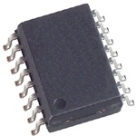
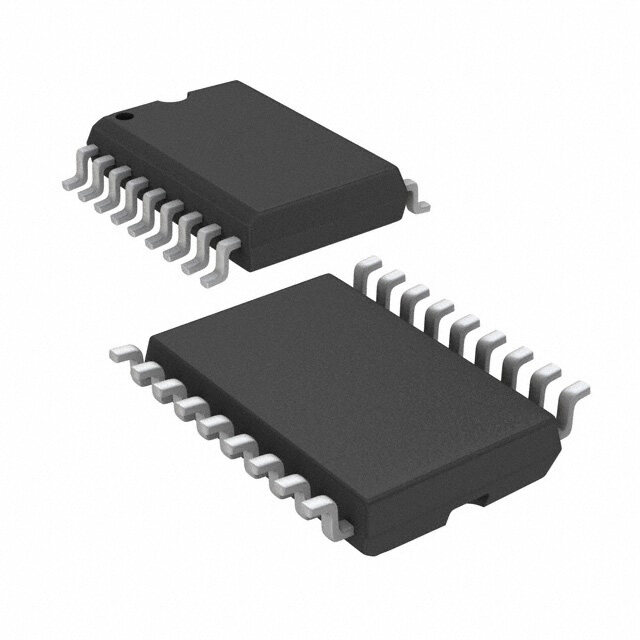
| 描述 | IC DAC 8BIT MULTIPLY HS 16-SOIC |
| 产品分类 | |
| 品牌 | Analog Devices Inc |
| 数据手册 | |
| 产品图片 |
|
| 产品型号 | DAC08CS |
| rohs | 不符合限制有害物质指令(RoHS)规范要求 |
| 产品系列 | - |
| 产品培训模块 | http://www.digikey.cn/PTM/IndividualPTM.page?site=cn&lang=zhs&ptm=19145http://www.digikey.cn/PTM/IndividualPTM.page?site=cn&lang=zhs&ptm=18614http://www.digikey.cn/PTM/IndividualPTM.page?site=cn&lang=zhs&ptm=26125http://www.digikey.cn/PTM/IndividualPTM.page?site=cn&lang=zhs&ptm=26140http://www.digikey.cn/PTM/IndividualPTM.page?site=cn&lang=zhs&ptm=26150http://www.digikey.cn/PTM/IndividualPTM.page?site=cn&lang=zhs&ptm=26147 |
| 位数 | 8 |
| 供应商器件封装 | 16-SOIC |
| 包装 | 管件 |
| 安装类型 | 表面贴装 |
| 封装/外壳 | 16-SOIC(0.154",3.90mm 宽) |
| 工作温度 | -40°C ~ 85°C |
| 建立时间 | 85ns |
| 数据接口 | 并联 |
| 标准包装 | 48 |
| 电压源 | 双 ± |
| 转换器数 | 1 |
| 输出数和类型 | 2 电流,单极 |
| 采样率(每秒) | 11.8M |


- 商务部:美国ITC正式对集成电路等产品启动337调查
- 曝三星4nm工艺存在良率问题 高通将骁龙8 Gen1或转产台积电
- 太阳诱电将投资9.5亿元在常州建新厂生产MLCC 预计2023年完工
- 英特尔发布欧洲新工厂建设计划 深化IDM 2.0 战略
- 台积电先进制程称霸业界 有大客户加持明年业绩稳了
- 达到5530亿美元!SIA预计今年全球半导体销售额将创下新高
- 英特尔拟将自动驾驶子公司Mobileye上市 估值或超500亿美元
- 三星加码芯片和SET,合并消费电子和移动部门,撤换高东真等 CEO
- 三星电子宣布重大人事变动 还合并消费电子和移动部门
- 海关总署:前11个月进口集成电路产品价值2.52万亿元 增长14.8%


PDF Datasheet 数据手册内容提取
8-Bit, High Speed, Multiplying D/A Converter Data Sheet DAC08 FEATURES Direct interface to all popular logic families with full noise immunity is provided by the high swing, adjustable threshold Fast settling output current: 85 ns logic input. Full-scale current prematched to ±1 LSB Direct interface to TTL, CMOS, ECL, HTL, PMOS High voltage compliance complementary current outputs are Nonlinearity to 0.1% maximum over temperature range provided, increasing versatility and enabling differential operation High output impedance and compliance: −10 V to +18 V to effectively double the peak-to-peak output swing. In many Complementary current outputs applications, the outputs can be directly converted to voltage Wide range multiplying capability: 1 MHz bandwidth without the need for an external op amp. All DAC08 series models Low FS current drift: ±10 ppm/°C guarantee full 8-bit monotonicity, and nonlinearities as tight as Wide power supply range: ±4.5 V to ±18 V ±0.1% over the entire operating temperature range are available. Low power consumption: 33 mW at ±5 V Device performance is essentially unchanged over the ±4.5 V to Low cost ±18 V power supply range, with 33 mW power consumption GENERAL DESCRIPTION attainable at ±5 V supplies. The compact size and low power consumption make the DAC08 The DAC08 series of 8-bit monolithic digital-to-analog convert- attractive for portable and military/aerospace applications; ers provide very high speed performance coupled with low cost devices processed to MIL-STD-883, Level B are available. and outstanding applications flexibility. DAC08 applications include 8-bit, 1 µs A/D converters, servo Advanced circuit design achieves 85 ns settling times with very motor and pen drivers, waveform generators, audio encoders low glitch energy and at low power consumption. Monotonic and attenuators, analog meter drivers, programmable power multiplying performance is attained over a wide 20 to 1 reference supplies, LCD display drivers, high speed modems, and other current range. Matching to within 1 LSB between reference and applications where low cost, high speed, and complete full-scale currents eliminates the need for full-scale trimming in input/output versatility are required. most applications. FUNCTIONAL BLOCK DIAGRAM (MSB) (LSB) V+ VLC B1 B2 B3 B4 B5 B6 B7 B8 13 1 5 6 7 8 9 10 11 12 DAC08 BIAS 4 IOUT NETWORK 2 CURRENT VREF (+) 14 SWITCHES IOUT 15 VREF (–) REFERENCE AMPLIFIER COM1P6 V–3 00268-C-001 Figure 1. Rev. D Document Feedback Information furnished by Analog Devices is believed to be accurate and reliable. However, no responsibility is assumed by Analog Devices for its use, nor for any infringements of patents or other One Technology Way, P.O. Box 9106, Norwood, MA 02062-9106, U.S.A. rights of third parties that may result from its use. Specifications subject to change without notice. No license is granted by implication or otherwise under any patent or patent rights of Analog Devices. Tel: 781.329.4700 ©2002–2016 Analog Devices, Inc. All rights reserved. Trademarks and registered trademarks are the property of their respective owners. Technical Support www.analog.com
DAC08 Data Sheet TABLE OF CONTENTS Features .............................................................................................. 1 Application Information ................................................................ 14 General Description ......................................................................... 1 Reference Amplifier Setup ........................................................ 14 Functional Block Diagram .............................................................. 1 Reference Amplifier Compensation for Multiplying Revision History ............................................................................... 2 Applications ................................................................................ 14 Specifications ..................................................................................... 3 Logic Inputs................................................................................. 14 Electrical Characteristics ............................................................. 3 Analog Output Currents ........................................................... 14 Typical Electrical Characteristics ............................................... 4 Power Supplies ............................................................................ 15 Absolute Maximum Ratings ............................................................ 5 Temperature Performance......................................................... 15 Thermal Resistance ...................................................................... 5 Multiplying Operation ............................................................... 15 ESD Caution .................................................................................. 5 Settling Time ............................................................................... 15 Pin Configuration and Function Descriptions ............................. 6 Analog Devices Current Output DACs ....................................... 17 Test and Burn-In Circuits ................................................................ 7 Outline Dimensions ....................................................................... 18 Typical Performance Characteristics ............................................. 8 Ordering Guide .......................................................................... 19 Basic Connections .......................................................................... 11 REVISION HISTORY 3/16—Rev. C to Rev. D 2/02—Rev. A to Rev. B Added Thermal Resistance Section ............................................... 5 Edits to Specifications ....................................................................... 2 Changes to Table 4 ............................................................................ 5 Edits to Absolute Maximum Ratings .............................................. 3 Change to Figure 29 ....................................................................... 12 Edits to Ordering Guide ................................................................... 3 Updated Outline Dimensions ....................................................... 18 Edits to Wafer Test Limits ................................................................ 5 Changes to Ordering Guide .......................................................... 10 Edit to Figure 13 ................................................................................ 8 Edits to Figures 14 and 15 ................................................................ 9 11/04—Rev. B to Rev. C Changed SO to SOIC ......................................................... Universal Removed DIE ...................................................................... Universal Changes to Figure 30, Figure 31, Figure 32 ................................. 12 Change to Figure 33 ....................................................................... 15 Added Table 4 .................................................................................. 16 Updated Outline Dimensions ....................................................... 17 Changes to Ordering Guide .......................................................... 18 Rev. D | Page 2 of 21
Data Sheet DAC08 SPECIFICATIONS ELECTRICAL CHARACTERISTICS V = ±15 V, I = 2.0 mA, –55°C ≤ T ≤ +125°C for DAC08/DAC08A, 0°C ≤ T ≤ +70°C for DAC08E and DAC08H, −40°C to +85°C for S REF A A DAC08C, unless otherwise noted. Output characteristics refer to both IOUT and IOUT. Table 1. DAC08A/DAC08H DAC08E DAC08C Parameter Symbol Test Conditions/Comments Min Typ Max Min Typ Max Min Typ Max Unit RESOLUTION 8 8 8 Bits MONOTONICITY 8 8 8 Bits NONLINEARITY NL ±0.1 ±0.19 ±0.39 %FS SETTLING TIME t To ±1/2 LSB, all bits switched 85 135 85 150 85 150 ns S on or off, T = 25°C1 A PROPAGATION DELAY Each Bit t T = 25°C1 35 60 35 60 35 60 ns PLH A All Bits Switched t 35 60 35 60 35 60 ns PHL FULL-SCALE TEMPCO1 TCI ±10 ±50 ±10 ±80 ±10 ±80 ppm/°C FS DAC08E ±50 OUTPUT VOLTAGE Compliance V Full-scale current OC (True Compliance) Change <1/2 LSB, R > −10 +18 −10 +18 –10 +18 V OUT 20 MΩ typ FULL RANGE CURRENT I V = 10.000 V R14, R15 = 1.984 1.992 2.000 1.94 1.99 2.04 1.94 1.99 2.04 mA FR4 REF 5.000 kΩ T = 25°C A FULL RANGE I I − I ±0.5 ±4 ±1 ±8 ±2 ±16 µA FRS FR4 FR2 SYMMETRY ZERO-SCALE CURRENT I 0.1 1 0.2 2 0.2 4 µA ZS OUTPUT CURRENT I R14, R15 = 5.000 kΩ 2.1 2.1 2.1 mA OR1 RANGE I V = +15.0 V, V− = −10 V OR2 REF V = +25.0 V, 4.2 4.2 4.2 mA REF V− = −12 V OUTPUT CURRENT I = 2 mA 25 25 25 nA REF NOISE LOGIC INPUT LEVELS Logic 0 V V = 0 V 0.8 0.8 0.8 V IL LC Logic 1 V 2 2 2 V IL LOGIC INPUT CURRENT V = 0 V LC Logic 0 I V = −10 V to +0.8 V −2 −10 −2 −10 −2 −10 µA IL IN Logic 1 I V = 2.0 V to 18 V 0.002 10 0.002 10 0.002 10 µA IH IN LOGIC INPUT SWING V V− = −15 V −10 +18 −10 +18 −10 +18 V IS LOGIC THRESHOLD V V = ±15 V1 −10 +13.5 −10 +13.5 −10 +13.5 V THR S RANGE REFERENCE BIAS I −1 −3 −1 −3 −1 −3 µA 15 CURRENT REFERENCE INPUT dI/dt R = 200 Ω 4 8 4 8 4 8 mA/µs EQ SLEW RATE R = 100 Ω L C = 0 pF. See Figure 7.1 C Rev. D | Page 3 of 21
DAC08 Data Sheet DAC08A/DAC08H DAC08E DAC08C Parameter Symbol Test Conditions/Comments Min Typ Max Min Typ Max Min Typ Max Unit POWER SUPPLY PSSI V+ = 4.5 V to 18 V ±0.0003 ±0.01 ±0.0003 ±0.01 ±0.0003 ±0.01 %∆I / FS+ O SENSITIVITY %∆V+ PSSI V− = −4.5 V to −18 V ±0.002 ±0.01 ±0.002 ±0.01 ±0.002 ±0.01 %∆I / FS– O %∆V− I = 1.0 mA REF POWER SUPPLY I+ V = ±5 V, I = 1.0 mA 2.3 3.8 2.3 3.8 2.3 3.8 mA S REF CURRENT I− −4.3 −5.8 −4.3 −5.8 −4.3 −5.8 mA I+ V = +5 V, −15 V 2.4 3.8 2.4 3.8 2.4 3.8 mA S I− I = 2.0 mA −6.4 −7.8 −6.4 −7.8 −6.4 −7.8 mA REF I+ V = ±15 V 2.5 3.8 2.5 3.8 2.5 3.8 mA S I− I = 2.0 mA −6.5 −7.8 −6.5 −7.8 −6.5 −7.8 mA REF POWER DISSIPATION P ±5 V, I = 1.0 mA +5 V, 33 48 33 48 33 48 mW D REF −15 V I = 2.0 mA ±15 V, I = 108 136 103 136 108 136 mW REF REF 2.0 mA 135 174 135 174 135 174 mW 1 Guaranteed by design. TYPICAL ELECTRICAL CHARACTERISTICS VS = ±15 V, and IREF = 2.0 mA, unless otherwise noted. Output characteristics apply to both IOUT and IOUT. Table 2. Parameter Symbol Test Conditions/Comments All Grades Typical Unit REFERENCE INPUT SLEW RATE dI/dt 8 mA/µs PROPAGATION DELAY t , t T = 25°C, any bit 35 ns PLH PHL A SETTLING TIME t To ±1/2 LSB, all bits switched on or 85 ns S off, T = 25°C A Rev. D | Page 4 of 21
Data Sheet DAC08 ABSOLUTE MAXIMUM RATINGS THERMAL RESISTANCE Table 3. Parameter Rating θ is specified for worst case mounting conditions, that is, θ is JA JA Operating Temperature specified for device in socket for CERDIP, PDIP, and LCC DAC08AQ, DAC08Q −55°C to +125°C packages; θJA is specified for device soldered to printed circuit DAC08HQ, DAC08EQ, DAC08CQ 0°C to +70°C board for SOIC package. DAC08CP, DAC08CS −40°C to +85°C Table 4. Thermal Resistance Junction Temperature (T) −65°C to +150°C J Package Type θ θ Unit Storage Temperature Q Package −65°C to +150°C JA JC 16-Lead CERDIP (Q) 100 16 °C/W Storage Temperature P Package −65°C to +125°C 16-Lead PDIP (P) 82 39 °C/W Lead Temperature (Soldering, 60 sec) 300°C 20-Terminal LCC (RC) 76 36 °C/W V+ Supply to V− Supply 36 V 16-Lead SOIC (S) 111 35 °C/W Logic Inputs V− to V− + 36 V V V− to V+ LC ESD CAUTION Analog Current Outputs (at V = 15 V) 4.25 mA S− Reference Input (V to V ) V− to V+ 14 15 Reference Input Differential Voltage (V to V ) ±18 V 14 15 Reference Input Current (I ) 5.0 mA 14 Stresses at or above those listed under Absolute Maximum Ratings may cause permanent damage to the product. This is a stress rating only; functional operation of the product at these or any other conditions above those indicated in the operational section of this specification is not implied. Operation beyond the maximum operating conditions for extended periods may affect product reliability. Rev. D | Page 5 of 21
DAC08 Data Sheet PIN CONFIGURATION AND FUNCTION DESCRIPTIONS VLC 1 16 COMP IOUT 2 15 VREF (–) V– 3 14 VREF (+) DAC08 IOUT 4 13 V+ TOP VIEW (MSB) B1 5 (Not To Scale) 12 B8 (LSB) B2 6 11 B7 BB34 78 190 BB65 00268-C-002 Figure 2. 16-Lead Dual In-Line Package (PDIP and CERDIP) V+ 1 16 B8 (LSB) VREF (+) 2 15 B7 VREF (–) 3 14 B6 DAC08 COMP 4 13 B5 TOP VIEW VLC 5 (Not To Scale) 12 B4 IOUT 6 11 B3 IOVU–T 78 190 BB21 (MSB) 00268-C-003 Figure 3. 16-Lead Standard Small Outline Package (SOIC_N) IOUTVLCNC COMP V (–)REF 3 2 1 20 19 V– 4 18 VREF (+) IOUT 5 DAC08 17 V+ NC 6 TOP VIEW 16 NC (Not To Scale) (MSB) B1 7 15 B8(LSB) B2 8 14 B7 NCB39 = N1B40O 1CNC1O1NB52NE1B63CT 00268-C-004 Figure 4. DAC08RC/883 20-Terminal Ceramic Leadless Chip Carrier (LCC) Rev. D | Page 6 of 21
Data Sheet DAC08 TEST AND BURN-IN CIRCUITS +VREF RREF OPTIONAL RESISTOR FOR OFFSET INPUTS RIN RL 14 4 REQ≈ 200Ω 0V RP RL TYPICALVALUES: 15 16 2 R+VININ==51k0ΩV NO CAP 00268-C-006 Figure 5. Pulsed Reference Operation C2 R1 = 9kΩ +18V C1 = 0.001µF C2, C3 = 0.01µF C1 R1 16 15 14 13 12 11 10 9 DAC08 1 2 3 4 5 6 7 8 C3 –18V MIN 00268-C-007 Figure 6. Burn-In Circuit Rev. D | Page 7 of 21
DAC08 Data Sheet TYPICAL PERFORMANCE CHARACTERISTICS ALL BITS SWITCHED ON 1V 2.4V 1V 2.5V 0.4V 0.5V –1/2LSB –0.5mA SEOTUTTLPINUGT+1/2LS0BV IOUT –2.5mAREQ≈ 2001Ω00mV 200ns/DIVISION 200ns 00268-C-008 SETTLING1T0ImMVEFIXTURE 5500nnss/DIVISION 00268-C-011 RL = 100Ω IFS=2mA,RL=1kΩ CC = 0 1/2LSB=4µA Figure 7. Fast Pulsed Reference Operation Figure 10. Full-Scale Settling Time 5 TA = TMIN TO TMAX LIMIT FOR ALLBITS HIGH V– =–15V 0mA IOUT A) 4 m T ( N RE 3 R 1.0mA U C T U P 2 T U O 2.0mA IOUT , FS LVI–M =IT– F5VOR (0000|0000) IREF = 2mA (1111|100268-C-009111) I 100 1 IREF, REFE2RENCE CUR3RENT (mA)4 5 00268-C-012 Figure 8. True and Complementary Output Operation Figure 11. Full-Scale Current vs. Reference Current 5mV 2V 500 2.4V 400 s) n Y ( A 0.4V DEL300 0V N O TI 8µA GA200 1LSB = 7.8µA A P 0 RO P 100mV 50ns/DIVISION 50ns 00268-C-010 1000 0.0IF0S5, O0.0U1TP0U.02T FU0.L05L-S0.C10AL0E.2 0CUR0.R50EN1T.01 0L(mS2AB.0) 0= 615n.0A0 10.0000268-C-013 Figure 9. LSB Switching Figure 12. LSB Propagation Delay vs. IFS Rev. D | Page 8 of 21
Data Sheet DAC08 10 2.0 8 R14 = R15 = 1kΩ RL≤500V 6 ALL BITS ON 1.6 B) 4 VR15 = 0V T (d 2 OUTPU–20 2 V (V)LC1.2 TIVE –4 1 V–TH0.8 A EL–6 CC = 15pF, VIN = 2.0V p-p R CENTERED AT +1.0V –8 LARGE SIGNAL 0.4 –10 CC =15pF, VIN = 50mV p-p –12 CENTERED AT +200mV SMALL SIGNAL –140.1 0.2 0F.5REQUE1N.0CY (MH2z).0 5.0 10.000268-C-014 0 –50 0 TEMPERA50TURE (°C) 100 150 00268-C-017 Figure 13. Reference Input Frequency Response Figure 16. VTH − VLC vs. Temperature 4.0 4.0 TA = TMIN TO TMAX ALL BITS ON TA = TMIN TO TMAX ALL BITS ON 3.6 3.6 3.2 3.2 T (mA)2.8 NROANTEG:E P IOSS AITLIWVEA YCSO (MVM+)O–N1-.M5VODE T (mA)2.8 N2.4 N2.4 E E URR2.0 V– =–15V V– =–5V V+ = +15V URR2.0 V– =–15V V– =–5V IREF = 2mA UT C1.6 IREF = 2mA UT C1.6 P P T T OU1.2 IREF = 1mA OU1.2 IREF = 1mA 0.8 0.8 0.4 IREF = 0.2mA 0.4 IREF = 0.2mA 0–14 –V1105, REF–E6RENC–E2 COMM2ON-MOD6E VOL1T0AGE (V1)4 18 00268-C-015 0–14 –10 –6 OU–T2PUTVO2LTAGE6(V) 10 14 18 00268-C-018 Figure 14. Reference Amplifier Common-Mode Range Figure 17. Output Current vs. Output Voltage (Output Voltage Compliance) 10 28 24 8 20 V) 16 µT (A) 6 TAGE ( 12 SHADED AREA INDICATES PERMISSIBLE PU OL 8 OUTPUT VOLTAGE RANGE FOR V– =–15V. LOGIC IN 4 OUTPUT V 40 IFSROEEERF ≤OO 2UT.HT0PmEURAT .V C– UORRR IERNEFT, VS. OUTPUT VOLTAGE CURVE. 2 –4 –8 0–12 –8 –4LOGIC0 INPUT V4OLTAG8E (V) 12 16 00268-C-016 –12 –50 0 TEMPERA50TURE (°C) 100 150 00268-C-019 Figure 15. Logic Input Current vs. Input Voltage Figure 18. Output Voltage Compliance vs. Temperature Rev. D | Page 9 of 21
DAC08 Data Sheet 1.8 10 BITS MAY BE HIGH OR LOW 1.6 9 1.4 mA) 8 NT (mA)1.2 B1 RRENT ( 76 I– WITH IREF = 2mA UT CURRE10..08 IREF = 2.0mA UPPLY CU 54 I– WITH IREF = 1mA OUTP0.6 B2 WER S 3 I– WITH IREF = 0.2mA 0.4 V– =–5V B4 B3 B5 PO 2 I+ 0.2 �V�–� �=–15V 1 0–1N2OTE:–8 –L4OGIC IN0PUT VOL4TAGE (V8) 12 16 00268-C-020 00 –2 –V4–, NE–6GATIV–8E PO–W10ER S–U12PPL–Y1 4(V d–c1)6 –18 –2000268-C-022 B1 THROUGH B8 HAVE IDENTICAL TRANSFER CHARACTERISTICS. BITS ARE FULLY SWITCHED WITH LESS THAN 1/2 LSB ERROR, AT LESS THAN±100mV FROM ACTUAL THRESHOLD. THESE SWITCHING POINTS ARE GUARANTEED TO LIE BETWEEN 0.8V AND 2.0V OVER THE OPERATING TEMPERATURE RANGE (VLC = 0.0V). Figure 19. Bit Transfer Characteristics Figure 21. Power Supply Current vs. V− 10 10 ALL BITS HIGH OR LOW ALL BITS HIGH OR LOW 9 9 A)8 A) 8 m m ENT (7 I– ENT ( 7 V– =–15V I– URR6 URR 6 IREF = 2.0mA C C Y 5 Y 5 PL PL UP4 UP 4 S S WER 3 I+ WER 3 V+ = +15V I+ PO2 PO 2 1 1 00 2 4V+, PO6SITIVE8 POW10ER SU12PPLY1 4(V dc)16 18 20 00268-C-021 0 –50 0 TEMPERA5T0URE (°C) 100 150 00268-C-023 Figure 20. Power Supply vs. V+ Figure 22. Power Supply Current vs. Temperature Rev. D | Page 10 of 21
Data Sheet DAC08 BASIC CONNECTIONS +VREF IINRREF IREF VIN 1144 RIN 1155 IREF≥PEAK NEGATIVE SWING OF IIN RREF≈R15 +VREF RREF 14 R15 (OPTIONAL) VIN 15 IHMI+GPVEHRD EINAFPNMUCUTEST BE ABOVE PEAK POSITIVE SWING OF VIN 00268-C-024 Figure 23. Accommodating Bipolar References MSB LSB B1B2B3B4B5B6B7B8 IREF +VREF RREF VREF(+)145 6 7 8 9 1011124 IO (R14) VREF(–) 2 R15 15 3 16 13 1 IO V– V+ FOR FIXED REFERENCE, CC TTL OPERATION, TYPICAL VALUES ARE: COMP VREF = 10.000V IAIOFLR +L = ILO+OR V=GR RIEIFECFRF SF×TO22AR55T56ES0.1µF V–0.1µF V+ VLC RRCVLRC1C5E = F== 0 = 0R. 0V5R1. E0µ(GF0F0RkOΩUND) 00268-C-025 Figure 24. Basic Positive Reference Operation MSB LSB B1B2B3B4B5B6B7B8 EO B1 B2 B3 B4 B5 B6 B7 B8 IO IO EO EO IO 5.000kΩ FULL RANGE 1 1 1 1 1 1 1 1 1.992 0.000 –9.960 –0.000 IREF = 2.000mA 4 HALF SCALE +LSB 1 0 0 0 1 0 0 1 1.008 0.984 –5.040 –4.920 14 5.000kΩ HALF SCALE 1 0 0 0 1 0 0 0 1.000 0.992 –5.000 –4.960 2 HALF SCALE–LSB 0 1 1 1 0 1 1 1 0.992 1.000 –4.960 –5.000 IO EO ZZEERROO SSCCAALLEE +LSB 00 00 00 00 00 00 00 10 00..000080 11..998942 –00.0.00400 ––99..992600 00268-C-026 Figure 25. Basic Unipolar Negative Operation 10V MSB LSB B1B2B3B4B5B6B7B8 10kΩ 10kΩ B1 B2 B3 B4 B5 B6 B7 B8 EO EO IO POS. FULL RANGE 1 1 1 1 1 1 1 1 –9.920 +10.000 IREF = 2.000mA 14 4 EO PZEORSO. F SUCLALL REA +NLGSEB–LSB 11 10 10 10 10 10 10 01 ––90..804800 ++90..912600 2 ZERO SCALE 1 0 0 0 0 0 0 0 0.000 +0.080 IO EO ZNNEEERGGO.. FF SUUCLLALLL SSECC–AALLLSEEB +LSB 000 100 100 100 100 100 100 110 +++1090..09.0820000 ––099.0..89042000 00268-C-027 Figure 26. Basic Bipolar Output Operation Rev. D | Page 11 of 21
DAC08 Data Sheet LOW T.C. VREF 4.5kΩ 14 10V IREF (+)≈2mA 39kΩ 10kΩ ≈1V 15 POT AP5PkRΩOX 00268-C-028 Figure 27. Recommended Full-Scale Adjustment Circuit RREF 14 IO 4 IO –VREF R15 15 2 IFS≈–RVRREEFF NRBOIRAETSFE SCEUTRSR EIFNS;T R C1A5N ISC EFLOLRATION. 00268-C-029 Figure 28. Basic Negative Reference Operation 10kΩ 5.0kΩ 15V MSB LSB B1B2B3B4B5B6B7B8 +15V 2 10VVO 6 5.000kΩ IO B1 B2 B3 B4 B5 B6 B7 B8 EO 4 POS. FULL RANGE 1 1 1 1 1 1 1 1 +4.960 REF01* 5 AD8671 EO ZERO SCALE 1 0 0 0 0 0 0 0 0.000 5.0kΩ 2 NEG. FULL SCALE +1LSB 0 0 0 0 0 0 0 1 –4.960 V+ –V CC VLC IO NEG. FULL SCALE 0 0 0 0 0 0 0 0 –5.000 *OR AD4R01 +15V–15V –15V 00268-C-030 Figure 29. Offset Binary Operation RL IO 4 IO AD8671 EO 2 0 TO–IFR×RL 255 IFR = 2 5 6 IREF FCTOOOR NG NCREOOCMUTNP ILDNE.VMEERNTTINAGR YIN OPUUTT POUFT O (OP PAEMRPA TTOIO INO A(PSI NA 2N):E CGOANTNIVEEC LTO IOG I(CP IDNA 4C)). 00268-C-031 Figure 30. Positive Low Impedance Output Operation IO AD8671 EO 4 0 TO–IFR×RL 2 IO RL 255 IFR = 2 5 6 IREF FCTOOOR NG NCREOOCMUTNP NLDOE.MNIENNVTEARRTYIN OGU ITNPPUUTT (OOFP EORPA ATMIOPN T AOS I OA ( NPIENG 2A):T CIVOEN LNOEGCITC IDOA (PCI)N. 4) 00268-C-032 Figure 31. Negative Low Impedance Output Operation Rev. D | Page 12 of 21
Data Sheet DAC08 VTH = VLC 1.4V ECL CMOS,HVT+L,NMOS 15V CMOS 15V VTH = 7.6V TTL,DTL, VTH=1.4V 9.1kΩ 13kΩ 20kΩ VLC 2N3904 2N3904 "A" 2N3904 "A" 2N3904 VLC 6.2kΩ 0.1µF 3kΩ 3kΩ 1 39kΩ TO PIVNL 1C 20kΩ TO PINVL 1C R3 6.2kΩ 400µA –5.2V TEMPERATURE COMPENSATING VLC CIRCUITS 00268-C-033 Figure 32. Interfacing with Various Logic Families Rev. D | Page 13 of 21
DAC08 Data Sheet APPLICATION INFORMATION REFERENCE AMPLIFIER SETUP For fastest response to a pulse, low values of R14 enabling small C values must be used. If Pin 14 is driven by a high impedance The DAC08 is a multiplying D/A converter in which the output C such as a transistor current source, none of the preceding values current is the product of a digital number and the input reference suffice, and the amplifier must be heavily compensated, which current. The reference current may be fixed or may vary from decreases overall bandwidth and slew rate. For R14 = 1 kΩ and nearly zero to 4.0 mA. The full-scale output current is a linear C = 15 pF, the reference amplifier slews at 4 mA/μs, enabling a function of the reference current and is given by C transition from I = 0 to I = 2 mA in 500 ns. REF REF 255 I I Operation with pulse inputs to the reference amplifier can be FR 256 REF accommodated by an alternate compensation scheme. This where I = I REF 14 technique provides lowest full-scale transition times. An internal In positive reference applications, an external positive reference clamp allows quick recovery of the reference amplifier from a voltage forces current through R14 into the VREF(+) terminal (Pin 14) cutoff (IREF = 0) condition. Full-scale transition (0 mA to 2 mA) of the reference amplifier. Alternatively, a negative reference may be occurs in 120 ns when the equivalent impedance at Pin 14 is 200 Ω applied to VREF(–) at Pin 15; reference current flows from ground and CC = 0. This yields a reference slew rate of 16 mA/μs, which through R14 into VREF(+) as in the positive reference case. This is relatively independent of the RIN and VIN values. negative reference connection has the advantage of a very high LOGIC INPUTS impedance presented at Pin 15. The voltage at Pin 14 is equal to The DAC08 design incorporates a unique logic input circuit that and tracks the voltage at Pin 15 due to the high gain of the internal enables direct interface to all popular logic families and provides reference amplifier. R15 (nominally equal to R14) cancels bias maximum noise immunity. This feature is made possible by the current errors; R15 may be eliminated with only a minor large input swing capability, 2 μA logic input current, and increase in error. completely adjustable logic threshold voltage. For V− = −15 V, the Bipolar references may be accommodated by offsetting V or REF logic inputs may swing between −10 V and +18 V. This enables Pin 15. The negative common-mode range of the reference direct interface with 15 V CMOS logic, even when the DAC08 amplifier is given by V – = V− plus (I × 1 kΩ) plus 2.5 V. CM REF is powered from a 5 V supply. Minimum input logic swing and The positive common-mode range is V+ less 1.5 V. minimum logic threshold voltage are given by When a dc reference is used, a reference bypass capacitor is V− + (I × 1 kΩ) + 2.5 V REF recommended. A 5.0 V TTL logic supply is not recommended The logic threshold may be adjusted over a wide range by as a reference. If a regulated power supply is used as a reference, placing an appropriate voltage at the logic threshold control pin R14 must be split into two resistors with the junction bypassed (Pin 1, V ). Figure 16 shows the relationship between V and to ground with a 0.1 μF capacitor. LC LC V over the temperature range, with V nominally 1.4 above TH TH For most applications, the tight relationship between I and I REF FS V . For TTL and DTL interface, simply ground Pin 1. When LC eliminates the need for trimming I If required, full-scale REF. interfacing ECL, an I = 1 mA is recommended. For interfacing REF trimming can be accomplished by adjusting the value of R14, or other logic families, see Figure 32. For general set-up of the logic by using a potentiometer for R14. An improved method of full- control circuit, note that Pin 1 sources 100 μA typical; external scale trimming that eliminates potentiometer T.C. effects is shown circuitry must be designed to accommodate this current. in the recommended full-scale adjustment circuit (Figure 27). Fastest settling times are obtained when Pin 1 sees a low Using lower values of reference current reduces negative power impedance. If Pin 1 is connected to a 1 kΩ divider, for example, supply current and increases reference amplifier negative common- it must be bypassed to ground by a 0.01 μF capacitor. mode range. The recommended range for operation with a dc ANALOG OUTPUT CURRENTS reference current is 0.2 mA to 4.0 mA. Both true and complemented output sink currents are provided REFERENCE AMPLIFIER COMPENSATION FOR MULTIPLYING APPLICATIONS where IO + IO = IFS. Current appears at the true (IO) output when a 1 (logic high) is applied to each logic input. As the binary count AC reference applications require the reference amplifier to be increases, the sink current at Pin 4 increases proportionally, in compensated using a capacitor from Pin 16 to V−. The value of the fashion of a positive logic DAC. When a 0 is applied to any this capacitor depends on the impedance presented to Pin 14; input bit, that current is turned off at Pin 4 and turned on at Pin 2. for R14 values of 1.0 kΩ, 2.5 kΩ, and 5.0 kΩ, minimum values A decreasing logic count increases IO as in a negative or inverted of C are 15 pF, 37 pF, and 75 pF. Larger values of R14 require C logic DAC. Both outputs may be used simultaneously. proportionately increased values of C for proper phase margin, C so the ratio of C (pF) to R14 (kΩ) = 15. C Rev. D | Page 14 of 21
Data Sheet DAC08 If one of the outputs is not required, it must be connected to The reference amplifier must be compensated by using a capacitor ground or to a point capable of sourcing I ; do not leave an from Pin 16 to V−. For fixed reference operation, a 0.01 µF FS unused output pin open. capacitor is recommended. For variable reference applications, refer to the Reference Amplifier Compensation for Multiplying Both outputs have an extremely wide voltage compliance Applications section. enabling fast direct current to voltage conversion through a resistor tied to ground or other voltage source. Positive compli- MULTIPLYING OPERATION ance is 36 V above V− and is independent of the positive supply. The DAC08 provides excellent multiplying performance with an Negative compliance is given by extremely linear relationship between I and I over a range of FS REF V− + (IREF × 1 kΩ) + 2.5 V 4 µA to 4 mA. Monotonic operation is maintained over a typical range of I from 100 µA to 4.0 mA. The dual outputs enable double the usual peak-to-peak load REF swing when driving loads in quasi-differential fashion. This SETTLING TIME feature is especially useful in cable driving, CRT deflection and The DAC08 is capable of extremely fast settling times, typically in other balanced applications such as driving center-tapped 85 ns at I = 2.0 mA. Judicious circuit design and careful board REF coils and transformers. layout must obtain full performance potential during testing POWER SUPPLIES and application. The logic switch design enables propagation delays of only 35 ns for each of the 8 bits. Settling time to within The DAC08 operates over a wide range of power supply voltages 1/2 LSB of the LSB is therefore 35 ns, with each progressively from a total supply of 9 V to 36 V. When operating at supplies larger bit taking successively longer. The MSB settles in 85 ns, thus of ±5 V or lower, I ≤ 1 mA is recommended. Low reference REF determining the overall settling time of 85 ns. Settling to 6-bit current operation decreases power consumption and increases accuracy requires about 65 ns to 70 ns. The output capacitance negative compliance (Figure 11), reference amplifier negative of the DAC08, including the package, is approximately 15 pF; common-mode range (Figure 14), negative logic input range therefore the output RC time constant dominates settling time if (Figure 15), and negative logic threshold range (Figure 16). For R > 500 Ω. example, operation at −4.5 V with I = 2 mA is not recommended L REF because negative output compliance reduces to near zero. Settling time and propagation delay are relatively insensitive to Operation from lower supplies is possible; however, at least logic input amplitude and rise and fall times, due to the high 8 V total must be applied to ensure turn on of the internal bias gain of the logic switches. Settling time also remains essentially network. constant for I values. The principal advantage of higher I REF REF values lies in the ability to attain a given output level with lower Symmetrical supplies are not required, as the DAC08 is quite load resistors, thus reducing the output RC time constant. insensitive to variations in supply voltage. Battery operation is feasible because no ground connection is required; however, an Measuring the settling time requires the ability to accurately artificial ground can ensure logic swings, etc., remain between resolve ±4 µA; therefore a 1 kΩ load is needed to provide adequate acceptable limits. Power consumption is calculated as follows: drive for most oscilloscopes. The settling time fixture shown in P =(I+)(V+)+(I−)(V−) Figure 33 uses a cascade design to permit driving a 1 kΩ load D with less than 5 pF of parasitic capacitance at the measurement A useful feature of the DAC08 design is that supply current is node. At I values of less than 1.0 mA, excessive RC damping REF constant and independent of input logic states. This is useful in of the output is difficult to prevent while maintaining adequate cryptographic applications and further reduces the size of the sensitivity. However, the major carry from 01111111 to 10000000 power supply bypass capacitors. provides an accurate indicator of settling time. This code change TEMPERATURE PERFORMANCE does not require the normal 6.2 time constants to settle to within ±0.2% of the final value, and thus settling time is observed at The nonlinearity and monotonicity specifications of the DAC08 lower values of I . REF are guaranteed to apply over the entire rated operating temperature range. Full-scale output current drift is low, typically ±10 ppm/°C, DAC08 switching transients or “glitches” are very low and can with zero-scale output current and drift essentially negligible be further reduced by small capacitive loads at the output at a compared to 1/2 LSB. minor sacrifice in settling time. Fastest operation can be obtained by using short leads, minimizing output capacitance and load The temperature coefficient of the reference resistor R14 must resistor values, and by adequate bypassing at the supply, reference, match and track that of the output resistor for minimum overall and V terminals. Supplies do not require large electrolytic bypass LC full-scale drift. Settling times of the DAC08 decrease approximately capacitors because the supply current drain is independent of 10% at –55°C. At +125°C, an increase of about 15% is typical. input logic states; 0.1 µF capacitors at the supply pins provide full transient protection. Rev. D | Page 15 of 21
DAC08 Data Sheet VL +5V FORTURN-ON,VL=2.7V FORTURN-OFF,VL=0.7V 1kΩ 1µF 50µF MINIMUM Q2 CAPACITANCE VCL 1kΩ VOUT 1× +0.4V 0.7V Q1 PROBE 0V 0.1µF VIN 1µF 0V +VREF RREF 145 6 7 8 9 1011124 100kΩ 2kΩ 15kΩ 0–.01.µ4FV DAC08 IOUT R15 2 15 13 3 16 –15V 0.01µF 0.1µF +15V –15V 0.1µF 00268-C-034 Figure 33. Settling Time Measurement Rev. D | Page 16 of 21
Data Sheet DAC08 ANALOG DEVICES, INC., CURRENT OUTPUT DACs Table 4 lists the latest DACs available from Analog Devices. Table 5. Model Bits Outputs Interface Package Comments AD5425 8 1 SPI, 8-bit load MSOP-10 Fast 8-bit load; see also AD5426 AD5426 8 1 SPI MSOP-10 See also AD5425 fast load AD5450 8 1 SPI SOT23-8 See also AD5425 fast load AD5424 8 1 Parallel TSSOP-16 AD5429 8 2 SPI TSSOP-16 AD5428 8 2 Parallel TSSOP-20 AD5432 10 1 SPI MSOP-10 AD5451 10 1 SPI SOT23-8 AD5433 10 1 Parallel TSSOP-20 AD5439 10 2 SPI TSSOP-16 AD5440 10 2 Parallel TSSOP-24 AD5443 12 1 SPI MSOP-10 See also AD5452 and AD5444 AD5452 12 1 SPI SOT23-8 Higher accuracy version of AD5443; see also AD5444 AD5445 12 1 Parallel TSSOP-20 AD5444 12 1 SPI MSOP-10 Higher accuracy version of AD5443; see also AD5452 AD5449 12 2 SPI TSSOP-16 AD5415 12 2 SPI TSSOP-24 Uncommitted resistors AD5447 12 2 Parallel TSSOP-24 AD5405 12 2 Parallel LFCSP-40 Uncommitted resistors AD5453 14 1 SPI SOT23-8 AD5553 14 1 SPI MSOP-8 AD5556 14 1 Parallel TSSOP-28 AD5446 14 1 SPI MSOP-10 MSOP version of AD5453; compatible with AD5443, AD5432, and AD5426 AD5555 14 2 SPI TSSOP-16 AD5557 14 2 Parallel TSSOP-38 AD5543 16 1 SPI MSOP-8 AD5546 16 1 Parallel TSSOP-28 AD5545 16 2 SPI TSSOP-16 AD5547 16 2 Parallel TSSOP-38 Rev. D | Page 17 of 21
DAC08 Data Sheet OUTLINE DIMENSIONS 0.775 0.755 0.735 16 9 0.280 PIN 1 0.250 INDICATOR 1 0.240 8 TOP VIEW 0.100 0.325 BSC 0.195 0.310 0.210 0.130 0.300 MAX SIDE VIEW 0.115 0.015 0.150 MIN 0.015 0.130 GAUGE END VIEW PLANE 0.012 0.115 SEATING 0.010 PLANE 0.022 0.021 0.430 0.008 0.018 0.070 0.016 MAX 0.015 0.045 0.060 0.011 0.039 0.055 0.030COMPLIANTTO JEDEC STANDARDS MS-001-BB 03-07-2014-D Figure 34. 16-Lead Plastic Dual In-Line Package [PDIP] Narrow Body (N-16) Dimensions shown in inches 0.005 (0.13) MIN 0.098 (2.49) MAX 16 9 0.310 (7.87) 0.220 (5.59) 1 8 PIN 1 0.100 (2.54) BSC 0.320 (8.13) 0.290 (7.37) 0.840 (21.34) MAX 0.060 (1.52) 0.200 (5.08) 0.015 (0.38) MAX 0.150 0.200 (5.08) (3.81) 0.125 (3.18) MIN SEATING 0.015 (0.38) 0.023 (0.58) 0.070 (1.78) PLANE 15° 0.008 (0.20) 0.014 (0.36) 0.030 (0.76) 0° CONTROLLING DIMENSIONS ARE IN INCHES; MILLIMETER DIMENSIONS (IN PARENTHESES) ARE ROUNDED-OFF INCH EQUIVALENTS FOR REFERENCE ONLY AND ARE NOT APPROPRIATE FOR USE IN DESIGN. Figure 35. 16-Lead Ceramic Dual In-Line Package [CERDIP] (Q-16) Dimensions shown in inches and (millimeters) Rev. D | Page 18 of 21
Data Sheet DAC08 10.00 (0.3937) 9.80 (0.3858) 16 9 4.00 (0.1575) 6.20 (0.2441) 3.80 (0.1496) 1 8 5.80 (0.2283) 1.27 (0.0500) 0.50 (0.0197) BSC 45° 1.75 (0.0689) 0.25 (0.0098) 0.25 (0.0098) 1.35 (0.0531) 8° 0.10 (0.0039) 0° COPLANARITY SEATING 0.10 0.51 (0.0201) PLANE 0.25 (0.0098) 1.27 (0.0500) 0.31 (0.0122) 0.17 (0.0067) 0.40 (0.0157) COMPLIANTTO JEDEC STANDARDS MS-012-AC C(RINEOFNPEATRRREOENNLCLTEIHN EOGSN EDLSIYM)AEANNRDSEI AORRNOESU NANORDEET DAIN-PO MPFRIFLO LMPIIMRLELIATIMTEEER TFSEO; RIRN ECUQHSU EDI VIINMA LEDENENSSTIIOGSN NFS.OR 060606-A Figure 36. 16-Lead Standard Small Outline Package [SOIC_N] Narrow Body (R-16) Dimensions shown in millimeters and (inches) 0.200 (5.08) 0.075 (1.91) REF 0.100 (2.54) REF 0.100 (2.54) REF 0.064 (1.63) 0.095 (2.41) 0.015 (0.38) 0.075 (1.90) MIN 19 3 18 20 4 0.028 (0.71) 0.358 (9.09) 0.358 1 0.342 (8.69) (9.09) 0.011 (0.28) BOTTOM 0.022 (0.56) SQ MSAQX 0.007R (0 T.1Y8P) VIEW 0.050 (1.27) 0.075 (1.91) 14 8 BSC REF 13 9 45° TYP 0.088 (2.24) 0.055 (1.40) 0.150 (3.81) 0.054 (1.37) 0.045 (1.14) BSC CONTROLLING DIMENSIONS ARE IN INCHES; MILLIMETERS DIMENSIONS (IN PARENTHESES) ARE ROUNDED-OFF INCH EQUIVALENTS FOR REFERENCE ONLY AND ARE NOT APPROPRIATE FOR USE IN DESIGN Figure 37. 20-Terminal Ceramic Leadless Chip Carrier [LCC] (E-20-1) Dimensions shown in inches and (millimeters) ORDERING GUIDE Model1, 2, 3 NL Temperature Range Package Description Package Option No. Parts Per Container DAC08AQ ±0.10% −55°C to +125°C 16-Lead CERDIP Q-16 25 DAC08AQ/883C ±0.10% −55°C to +125°C 16-Lead CERDIP Q-16 25 DAC08HQ ±0.10% 0°C to 70°C 16-Lead CERDIP Q-16 25 DAC08Q ±0.19% −55°C to +125°C 16-Lead CERDIP Q-16 25 DAC08RC/883C ±0.19% −55°C to +125°C 20-Terminal LCC E-20-1 55 DAC08EQ ±0.19% 0°C to 70°C 16-Lead CERDIP Q-16 25 DAC08ES ±0.19% 0°C to 70°C 16-Lead SOIC R-16 47 DAC08ESZ ±0.19% 0°C to 70°C 16-Lead SOIC R-16 47 DAC08ESZ-REEL ±0.19% 0°C to 70°C 16-Lead SOIC R-16 2500 DAC08CP ±0.39% −40°C to +85°C 16-Lead PDIP N-16 25 DAC08CPZ ±0.39% −40°C to +85°C 16-Lead PDIP N-16 25 DAC08CS ±0.39% −40°C to +85°C 16-Lead SOIC R-16 47 DAC08CS-REEL ±0.39% −40°C to +85°C 16-Lead SOIC R-16 2500 DAC08CSZ ±0.39% −40°C to +85°C 16-Lead SOIC R-16 47 DAC08CSZ-REEL ±0.39% −40°C to +85°C 16-Lead SOIC R-16 2500 DAC08EPZ ±0.19% 0°C to 70°C 16-Lead PDIP N-16 25 1 Devices processed in total compliance to MIL-STD-883. Consult the factory for the 883 data sheet. 2 For availability and burn-in information on the SOIC package, contact your local sales office. 3 Z = RoHS Compliant Part. Rev. D | Page 19 of 21
DAC08 Data Sheet NOTES Rev. D | Page 20 of 21
Data Sheet DAC08 NOTES ©2002–2016 Analog Devices, Inc. All rights reserved. Trademarks and registered trademarks are the property of their respective owners. D00268-0-3/16(D) Rev. D | Page 21 of 21