 Datasheet下载
- 型号: CYV15G0101DXB-BBXC
- 制造商: Cypress Semiconductor
- 库位|库存: xxxx|xxxx
- 要求:
| 数量阶梯 | 香港交货 | 国内含税 |
| +xxxx | $xxxx | ¥xxxx |
查看当月历史价格
查看今年历史价格
CYV15G0101DXB-BBXC产品简介:
ICGOO电子元器件商城为您提供CYV15G0101DXB-BBXC由Cypress Semiconductor设计生产,在icgoo商城现货销售,并且可以通过原厂、代理商等渠道进行代购。 CYV15G0101DXB-BBXC价格参考。Cypress SemiconductorCYV15G0101DXB-BBXC封装/规格:接口 - 电信, Telecom IC Transceiver 100-TBGA (11x11)。您可以下载CYV15G0101DXB-BBXC参考资料、Datasheet数据手册功能说明书,资料中有CYV15G0101DXB-BBXC 详细功能的应用电路图电压和使用方法及教程。
Cypress Semiconductor Corp(赛普拉斯半导体公司)的CYV15G0101DXB-BBXC是一款属于接口 - 电信分类的器件,其应用场景主要集中在高速数据传输和通信领域。以下是该型号可能的应用场景:

1. 光纤通信系统:该器件适用于光纤网络中的信号处理和数据传输,支持高带宽需求的电信基础设施,如光纤到户(FTTH)或数据中心互联。

2. 无线基站:在4G/5G无线通信基站中,该芯片可用于实现高速数据接口,连接射频单元与基带处理单元,满足低延迟和高吞吐量的要求。

3. 以太网设备:适用于高速以太网交换机、路由器或其他网络设备,提供可靠的电信级数据传输性能,确保网络稳定性和效率。

4. 工业通信:在工业自动化领域,该器件可用于实时通信协议的支持,例如PROFINET、EtherCAT等,实现设备间的高效数据交互。

5. 测试与测量仪器:用于高性能示波器、信号发生器等测试设备中,提供精确的数据采集和传输能力。

6. 存储系统:在企业级存储阵列或固态硬盘控制器中,该芯片可作为高速接口组件,优化数据读写速度。

总之,CYV15G0101DXB-BBXC凭借其卓越的性能,广泛应用于需要高速、稳定数据传输的电信和网络相关领域。具体应用还需结合其详细技术参数和客户设计需求进一步确认。
| 参数 | 数值 |
| 产品目录 | 集成电路 (IC) |
| 描述 | IC TXRX HOTLINK 100-LBGA |
| 产品分类 | |
| 品牌 | Cypress Semiconductor Corp |
| 数据手册 | http://www.cypress.com/?docID=35742 |
| 产品图片 |
|
| 产品型号 | CYV15G0101DXB-BBXC |
| rohs | 无铅 / 符合限制有害物质指令(RoHS)规范要求 |
| 产品系列 | HOTlink II™ |
| 产品目录页面 | |
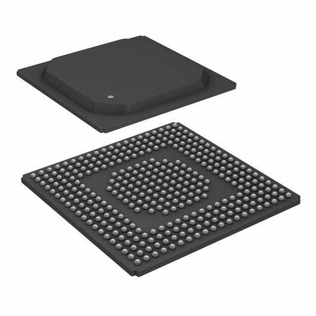
| 供应商器件封装 | 100-TBGA(11x11) |
| 其它名称 | 428-2921 |
| 功率(W) | * |
| 功能 | * |
| 包括 | * |
| 包装 | 托盘 |
| 安装类型 | 表面贴装 |
| 封装/外壳 | 100-LBGA |
| 工作温度 | 0°C ~ 70°C |
| 接口 | LVTTL |
| 标准包装 | 176 |
| 电压-电源 | 3.135 V ~ 3.465 V |
| 电流-电源 | 390mA |
| 电路数 | - |


- 商务部:美国ITC正式对集成电路等产品启动337调查
- 曝三星4nm工艺存在良率问题 高通将骁龙8 Gen1或转产台积电
- 太阳诱电将投资9.5亿元在常州建新厂生产MLCC 预计2023年完工
- 英特尔发布欧洲新工厂建设计划 深化IDM 2.0 战略
- 台积电先进制程称霸业界 有大客户加持明年业绩稳了
- 达到5530亿美元!SIA预计今年全球半导体销售额将创下新高
- 英特尔拟将自动驾驶子公司Mobileye上市 估值或超500亿美元
- 三星加码芯片和SET,合并消费电子和移动部门,撤换高东真等 CEO
- 三星电子宣布重大人事变动 还合并消费电子和移动部门
- 海关总署:前11个月进口集成电路产品价值2.52万亿元 增长14.8%


PDF Datasheet 数据手册内容提取
CYP15G0101DXB CYV15G0101DXB Single-channel HOTLink II™ Transceiver Single-channel HOTLink II™ Transceiver Features ■Compatible with ❐Fiber-optic modules ■Second-generation HOTLink® technology ❐Copper cables ■Compliant to multiple standards ❐Circuit board traces ❐ESCON®, DVB-ASI, fibre channel and gigabit ethernet ■JTAG boundary scan (IEEE802.3z) ■Built-in self-test (BIST) for at-speed link testing ❐CPRI™ compliant ❐CYV15G0101DXB compliant to SMPTE 259M and SMPTE ■Per-channel link quality indicator 292M ❐Analog signal detect ❐8B/10B encoded or 10-bit unencoded data ❐Digital signal detect ■Single-channel transceiver operates from 195 to 1500MBaud ■Low power 1.25 W at 3.3 V typical serial data rate ■Single 3.3 V supply ■Selectable parity check/generate ■100-ball BGA ■Selectable input clocking options ■Pb-free package option available ■Selectable output clocking options ■0.25 µ BiCMOS technology ■MultiFrame™ Receive Framer ❐Bit and byte alignment Functional Description ❐Comma or full K28.5 detect ❐Single- or multi-byte framer for byte alignment The CYP15G0101DXB[1] single-channel HOTLink II™ ❐Low-latency option transceiver is a point-to-point communications building block allowing the transfer of data over a high-speed serial link (optical ■Synchronous LVTTL parallel input and parallel output interface fiber, balanced, and unbalanced copper transmission lines) at ■Internal phase-locked loops (PLLs) with no external PLL signaling speeds ranging from 195 to 1500 MBaud. components The transmit channel accepts parallel characters in an input register, encodes each character for transport, and converts it to ■Dual differential PECL-compatible serial inputs serial data. The receive channel accepts serial data and converts ❐Internal DC-restoration it to parallel data, frames the data to character boundaries, ■Dual differential PECL-compatible serial outputs decodes the framed characters into data and special characters, and presents these characters to an output register. Figure1 ❐Source matched for driving 50 transmission lines illustrates typical connections between independent host ❐No external bias resistors required systems and corresponding CYP(V)15G0101DXB parts. As a ❐Signaling-rate controlled edge-rates second-generation HOTLink device, the CYP(V)15G0101DXB ■Optional elasticity buffer in receive path extends the HOTLinkII family with enhanced levels of integration and faster data rates, while maintaining serial-link ■Optional phase align buffer in transmit path compatibility (data, command, and BIST) with other HOTLink devices. Figure 1. HOTLinkII System Connections B B st DX DX 10 ost o 1 1 H H 10 10 Serial Link 10 10 m ystem 10 V)15G0 V)15G0 Syste S P( Backplane or Cabled P( Y Connections Y C C Note 1. CYV15G0101DXB refers to SMPTE 259M and SMPTE 292M compliant devices. CYP15G0101DXB refers to devices not compliant to SMPTE 259M and SMPTE 292M pathological test requirements. CYP(V)15G0101DXB refers both devices. CypressSemiconductorCorporation • 198 Champion Court • SanJose, CA 95134-1709 • 408-943-2600 Document Number: 38-02031 Rev. *P Revised November 9, 2017
CYP15G0101DXB CYV15G0101DXB The CYV15G0101DXB satisfies the SMPTE 259M and SMPTE The parallel I/O interface may be configured for numerous forms 292M compliance as per the EG34-1999 pathological test of clocking to provide the highest flexibility in system requirements. The transmit (TX) section of the architecture. In addition to clocking the transmit path interfaces CYP(V)15G0101DXB single-channel HOTLinkII consists of a from one or multiple sources, the receive interface may be byte-wide channel. The channel can accept either eight-bit data configured to present data relative to a recovered clock or to a characters or pre-encoded 10-bit transmission characters. Data local reference clock. characters are passed from the transmit input register to an The transmit and the receive channels contain BIST pattern embedded 8B/10B encoder to improve their serial transmission generators and checkers, respectively. This BIST hardware characteristics. These encoded characters are then serialized allows at-speed testing of the high-speed serial data paths in and output from dual positive ECL (PECL)-compatible both transmit and receive sections, as well as across the differential transmission-line drivers at a bit-rate of either 10 or interconnecting links. 20 times the input reference clock. HOTLinkII devices are ideal for a variety of applications where The receive (RX) section of the CYP(V)15G0101DXB parallel interfaces can be replaced with high-speed, single-channel HOTLinkII consists of a byte-wide channel. The point-to-point serial links. Some applications include channel accepts a serial bit-stream from one of two interconnecting backplanes on switches, routers, base-stations, PECL-compatible differential line receivers and, using a servers and video transmission systems. completely integrated PLL clock synchronizer, recovers the timing information necessary for data reconstruction. The The CYV15G0101DXB is verified by testing to be compliant to recovered bit-stream is deserialized and framed into characters, all the pathological test patterns documented in SMPTE 8B/10B decoded, and checked for transmission errors. EG34-1999, for both the SMPTE 259M and 292M signaling Recovered decoded characters are then written to an internal rates. The tests ensure that the receiver recovers data with no elasticity buffer, and presented to the destination host system. errors for the following patterns: The integrated 8B/10B encoder/decoder may be bypassed for 1.Repetitions of 20 ones and 20 zeros. systems that present externally encoded or scrambled data at 2.Single burst of 44 ones or 44 zeros. the parallel interface. 3.Repetitions of 19 ones followed by 1 zero or 19 zeros followed by 1 one. Transceiver Logic Block Diagram D[7:0]CT[1:0] D[7:0]ST[2:0] XX XX TT RR x10 x11 Phase Align Elasticity Buffer Buffer Encoder Decoder 8B/10B 8B/10B Framer Serializer Deserializer TX RX 2 12 T T NN U U II O O Document Number: 38-02031 Rev. *P Page 2 of 45
CYP15G0101DXB CYV15G0101DXB Logic Block Diagram = Internal Signal TRSTZ REFCLK+ Character-Rate Clock REFCLK– Transmit PLL Bit-Rate Clock TXRATE Clock Multiplier SPDSEL TXCLKO+ Character-Rate Clock TXCLKO– 2 TXMODE[1:0] Transmit Mode TXPER SCSEL TXTCXTDTX[[17O::00P]] 28 InputRegister 12 Phase-AlignBuffer 12 ParityCheck 12 BIST LFSR8B/10B 10 Shifter OOOOUUUUTTTT1122+–+– TXCKSEL TXLB H M L TXCLK 2 4 TXRST Output PARCTL Enable BOE[1:0] Latch OELE BIST Enable RXLE RX PLLaLt cEhnable Latch BISTLE Character-Rate Clock SDASEL LPEN Receive INSEL Signal LFI Monitor TIIIIXNNNNL1212B++–– RCeDlcooacvtkae &ry Shifter Framer 10B/8BBIST ElasticityBuffer OutputRegister 38 RRRXXXSDOT[P7[2:0:]0] PLL FRAMCHAR Clock 2 RXCLK+ RFEN Select RXCLK– RFMODE Delay DECMODE RXRATE RXCLKC+ RXMODE RXCKSEL TMS JTAG Boundary TCLK Scan TDI Controller TDO Document Number: 38-02031 Rev. *P Page 3 of 45
CYP15G0101DXB CYV15G0101DXB Contents Pin Configurations ...........................................................5 CYP(V)15G0101DXB AC Characteristics ......................27 Pin Descriptions ...............................................................6 Switching Waveforms for CYP(V)15G0101DXB HOTLinkII Operation ..................12 the HOTLink II Transmitter ...........................................29 CYP(V)15G0101DXB Transmit Data Path ................12 X3.230 Codes and Notation Conventions ....................33 Transmit Modes .........................................................13 Notation Conventions ................................................33 Transmit BIST ...........................................................15 8B/10B Transmission Code .......................................33 Serial Output Drivers .................................................16 Transmission Order ...................................................33 Transmit PLL Clock Multiplier ....................................16 Valid and Invalid Transmission Characters ...............33 CYP(V)15G0101DXB Receive Data Path .......................16 Use of the Tables for Generating Serial Line Receivers ................................................16 Transmission Characters ..................................................34 Signal Detect/Link Fault ............................................17 Use of the Tables for Checking Clock/Data Recovery .................................................18 the Validity of Received Transmission Characters ...........34 Deserializer/Framer ...................................................18 Ordering Information ......................................................40 10B/8B Decoder Block ..............................................19 Ordering Code Definitions .........................................40 Receive BIST Operation ............................................19 Package Diagram ............................................................41 Receive Elasticity Buffer ............................................20 Acronyms ........................................................................42 Receive Modes ..........................................................20 Document Conventions .................................................42 Power Control ............................................................20 Units of Measure .......................................................42 Output Bus ................................................................21 Document History Page .................................................43 Parity Generation ......................................................22 Sales, Solutions, and Legal Information ......................45 JTAG Support ............................................................23 Worldwide Sales and Design Support .......................45 Maximum Ratings ...........................................................25 Products ....................................................................45 Power-up Requirements ............................................25 PSoC® Solutions ......................................................45 DC Electrical Characteristics ........................................25 Cypress Developer Community .................................45 AC Test Loads and Waveforms .....................................26 Technical Support .....................................................45 Document Number: 38-02031 Rev. *P Page 4 of 45
CYP15G0101DXB CYV15G0101DXB Pin Configurations Top View 1 2 3 4 5 6 7 8 9 10 V IN2+ V OUT2– RXMODE TXMODE[1] IN1+ V OUT1– V A CC CC CC CC V IN2– TDO OUT2+ TXRATE TXMODE[0] IN1– #NC[2] OUT1+ V B CC CC RFEN LPEN RXLE RXCLKC+ RXRATE SDASEL SPDSEL PARCTL RFMODE INSEL C BOE[0] BOE[1] FRAMCHAR GND GND GND GND TMS TRSTZ TDI D BISTLE DECMODE OELE GND GND GND GND TCLK RXCKSEL TXCKSEL E RXST[2] RXST[1] RXST[0] GND GND GND GND TXPER REFCLK– REFCLK+ F RXOP RXD[1] RXD[5] GND GND GND GND TXOP TXCLKO+ TXCLKO– G RXD[0] RXD[2] RXD[6] LFI TXCT[1] TXD[6] TXD[3] TXCLK TXRST #NC[2] H V RXD[3] RXD[7] RXCLK– TXCT[0] TXD[5] TXD[2] TXD[0] #NC[2] V J CC CC V RXD[4] V RXCLK+ TXD[7] TXD[4] TXD[1] V SCSEL V K CC CC CC CC Bottom View 10 9 8 7 6 5 4 3 2 1 V OUT1– V IN1+ TXMODE[1] RXMODE OUT2– V IN2+ V CC CC CC CC A V OUT1+ #NC[2] IN1– TXMODE[0] TXRATE OUT2+ TDO IN2– V CC CC B INSEL RFMODE PARCTL SPDSEL SDASEL RXRATE RXCLKC+ RXLE LPEN RFEN C TDI TRSTZ TMS GND GND GND GND FRAMCHAR BOE[1] BOE[0] D TXCKSEL RXCKSEL TCLK GND GND GND GND OELE DECMODE BISTLE E REFCLK+ REFCLK– TXPER GND GND GND GND RXST[0] RXST[1] RXST[2] F TXCLKO– TXCLKO+ TXOP GND GND GND GND RXD[5] RXD[1] RXOP G #NC[2] TXRST TXCLK TXD[3] TXD[6] TXCT[1] LFI RXD[6] RXD[2] RXD[0] H V #NC[2] TXD[0] TXD[2] TXD[5] TXCT[0] RXCLK– RXD[7] RXD[3] V CC CC J V SCSEL V TXD[1] TXD[4] TXD[7] RXCLK+ V RXD[4] V CC CC CC CC K Note 2. #NC = Do Not Connect. Document Number: 38-02031 Rev. *P Page 5 of 45
CYP15G0101DXB CYV15G0101DXB Pin Descriptions CYP(V)15G0101DXB single-channel HOTLinkII Pin Name I/O Characteristics Signal Description Transmit Path Data Signals TXPER LVTTL output, Transmit path parity error. Active HIGH. Asserted (HIGH) if parity checking is enabled changes relative to (PARCTLLOW) and a parity error is detected at the encoder. This output is HIGH for one REFCLK[3] transmit character-clock period to indicate detection of a parity error in the character presented to the encoder. If a parity error is detected, the character in error is replaced with a C0.7 character to force a corresponding bad-character detection at the remote end of the link. This replacement takes place regardless of the encoded/un-encoded state of the interface. When BIST is enabled for the specific transmit channel, BIST progress is presented on this output. Once every 511 character times (plus a 16-character Word Sync Sequence when the receive channel is clocked by REFCLK, i.e., RXCKSEL=LOW), the TXPER signal pulses HIGH for one transmit-character clock period (if RXCKSEL=MID) or seventeen transmit-character clock periods (if RXCKSEL=LOW or HIGH) to indicate a complete pass through the BIST sequence. For RXCKSEL=LOW or HIGH, If TXMODE[1:0]=LL, then no Word Sync Sequence is sent in BIST, and TXPER pulses HIGH for one transmit-character clock period. This output also provides an indication of a phase-align buffer underflow/overflow condition. When the phase-align buffer is enabled (TXCKSELLOW, or TXCKSEL=LOW and TXRATE=HIGH), and an underflow/overflow condition is detected, TXPER is asserted and remains asserted until either an atomic Word Sync Sequence is transmitted or TXRST is sampled LOW to recenter the phase-align buffer. TXCT[1:0] LVTTL input, Transmit control. These inputs are captured on the rising edge of the transmit interface clock synchronous, as selected by TXCKSEL, and are passed to the encoder or transmit shifter. They identify sampled by how the TXD[7:0] characters are interpreted. When the encoder is enabled, these inputs TXCLK or determine if the TXD[7:0] character is encoded as data, a special character code, a K28.5 fill REFCLK[3] character or a Word Sync Sequence. When the encoder is bypassed, these inputs are interpreted as data bits. See Table1 for details. TXD[7:0] LVTTL input, Transmit data inputs. These inputs are captured on the rising edge of the transmit interface synchronous, clock as selected by TXCKSEL, and passed to the encoder or transmit shifter. sampled by When the encoder is enabled (TXMODE[1]LOW), TXD[7:0] specify the specific data or TXCLK or command character to be sent. When the encoder is bypassed, these inputs are interpreted REFCLK[3] as data bits of the 10-bit input character. See Table1 for details. TXOP LVTTL input, Transmit path odd parity. When parity checking is enabled (PARCTLLOW), the parity synchronous, captured at this input is XORed with the data on the TXD bus (and sometimes TXCT[1:0]) to internal pull-up, verify the integrity of the captured character. See Table2 for details. sampled by TXCLK or REFCLK[3] SCSEL LVTTL input, Special character select. Used in some transmit modes along with TXCTx[1:0] to encode synchronous, special characters or to initiate a Word Sync Sequence. When the transmit path is configured internal pull-down, to select TXCLK to clock the input register (TXCKSEL=MID or HIGH), SCSEL is captured sampled by relative to TXCLK. TXCLK or REFCLK[3] Note 3. When REFCLK is configured for half-rate operation (TXRATE=HIGH), this input is sampled (or the outputs change) relative to both the rising and falling edges of REFCLK. Document Number: 38-02031 Rev. *P Page 6 of 45
CYP15G0101DXB CYV15G0101DXB Pin Descriptions (continued) CYP(V)15G0101DXB single-channel HOTLinkII Pin Name I/O Characteristics Signal Description TXRST LVTTL input, Transmit clock phase reset. Active LOW. When sampled LOW, the transmit phase-align asynchronous, buffer is allowed to adjust its data-transfer timing (relative to the selected input clock) to allow internal pull-up, clean transfer of data from the input register to the encoder or transmit shifter. When TXRST sampled by is sampled HIGH, the internal phase relationship between the TXCLK and the internal REFCLK[4] character-rate clock is fixed and the device operates normally. When configured for half-rate REFCLK sampling of the transmit character stream (TXCKSEL = LOW and TXRATE = HIGH), assertion of TXRST is only used to clear phase-align buffer faults caused by highly asymmetric reference clock periods or reference clocks with excessive cycle-to-cycle jitter. During this alignment period, one or more characters may be added to or lost from all the associated transmit paths as the transmit phase-align buffers are adjusted. TXRST must be sampled LOW by a minimum of two consecutive rising edges of REFCLK to ensure the reset operation is initiated correctly on all channels. This input is ignored when both TXCKSEL and TXRATE are LOW, since the phase align buffer is bypassed. In all other configurations, TXRST should be asserted during device initialization to ensure proper operation of the phase-align buffer. TXRST should be asserted after the assertion and deassertion of TRSTZ, after the presence of a valid TXCLK and after allowing enough time for the TXPLL to lock to the reference clock (as specified by parameter t ). TXLOCK Transmit Path Clock and Clock Control TXCKSEL 3-level select static Transmit clock select. Selects the clock source used to write data into the transmit input control input[5] register of the transmit channel. When LOW, the input register is clocked by REFCLK.[4] When HIGH or MID, TXCLK is the input register clock for TXD[7:0] and TXCT[1:0]. When TXRATE=HIGH, configuring TXCKSEL = HIGH or MID is an invalid mode of operation. TXCLKO LVTTL output Transmit clock output. This true and complement output clock is synthesized by the transmit PLL and is synchronous to the internal transmit character clock. It has the same frequency as REFCLK (when TXRATE=LOW), or twice the frequency of REFCLK (when TXRATE=HIGH). This output clock has no direct phase relationship to REFCLK. TXRATE LVTTL input, Transmit PLL clock rate select. When TXRATE=HIGH, the transmit PLL multiplies static control input, REFCLK by 20 to generate the serial bit-rate clock. internal pull-down When TXRATE=LOW, the transmit PLL multiplies REFCLK by 10 to generate the serial bit-rate clock. See Table9 for a list of operating serial rates. When REFCLK is selected to clock the receive parallel interfaces (RXCKSEL = LOW), the TXRATE input also determines if the clocks on the RXCLK and RXCLKC outputs are full or half-rate. When TXRATE = HIGH (REFCLK is half-rate), the RXCLK± and RXCLKC+ output clocks are also half-rate clocks and follow the frequency and duty cycle of the REFCLK input. When TXRATE = LOW (REFCLK is full-rate), the RXCLK± and RXCLKC+ output clocks are also full-rate clocks and follow the frequency and duty cycle of the REFCLK input. When TXRATE=HIGH, configuring TXCKSEL = HIGH or MID is an invalid mode of operation. TXCLK LVTTL clock input, Transmit path input clock. This clock must be frequency-coherent to TXCLKO, but may internal pull-down be offset in phase. The internal operating phase of the input clock (relative to REFLCK or TXCLKO+) is adjusted when TXRST=LOW and locked when TXRST=HIGH. Transmit Path Mode Control TXMODE[1:0] 3-level select[5] Transmit operating mode. These inputs are interpreted to select one of nine operating static control inputs modes of the transmit path. See Table3 for a list of operating modes. Notes 4. When REFCLK is configured for half-rate operation (TXRATE=HIGH), this input is sampled (or the outputs change) relative to both the rising and falling edges of REFCLK. 5. 3-level select inputs are used for static configuration. They are ternary (not binary) inputs that make use of non-standard logic levels of LOW, MID, and HIGH. The LOW level is usually implemented by direct connection to VSS (ground). The HIGH level is usually implemented by direct connection to VCC (power). When not connected or allowed to float, a 3-level select input will self-bias to the MID level. Document Number: 38-02031 Rev. *P Page 7 of 45
CYP15G0101DXB CYV15G0101DXB Pin Descriptions (continued) CYP(V)15G0101DXB single-channel HOTLinkII Pin Name I/O Characteristics Signal Description Receive Path Data Signals RXD[7:0] LVTTL output, Parallel data output. These outputs change following the rising edge of the selected receive synchronous to the interface clock. RXCLK output (or When the decoder is enabled (DECMODE = HIGH or MID), these outputs represent either REFCLKinput[6] received data or a special character. The status of the received data is represented by the when values of RXST[2:0]. RXCKSEL = LOW) When the decoder is bypassed (DECMODE = LOW), RXD[7:0] become the higher order bits of the 10-bit received character. See Table13 for details. RXST[2:0] LVTTL output, Parallel status output. These outputs change following the rising edge of the selected synchronous to the receive interface clock. RXCLK output (or When the decoder is bypassed (DECMODE=LOW), RXST[1:0] become the two low-order REFCLKinput[6] bits of the 10-bit received character, while RXST[2]=HIGH indicates the presence of a when comma character in the output register. RXCKSEL = LOW) When the decoder is enabled (DECMODE=HIGH or MID), RXST[2:0] provide status of the received signal. See Table16 for a list of receive character status. RXOP 3-state, Receive path odd parity. When parity generation is enabled (PARCTLLOW), the parity LVTTL output, output is valid for the data on the RXD bus bits. synchronous to the When parity generation is disabled (PARCTL=LOW), this output driver is disabled (highZ). RXCLK output (or REFCLKinput[6] when RXCKSEL = LOW) Receive Path Clock and Clock Control RXCLK 3-state, Receive character clock output. When configured such that the output data path is clocked LVTTL output clock by the recovered clock (RXCKSEL = MID), these true and complement clocks are the receive interface clocks which are used to control timing of output data (RXD[7:0], RXST[2:0] and RXOP). This clock is output continuously at either the dual-character rate (1/20th the serial bit-rate) or character rate (1/10th the serial bit-rate) of the data being received, as selected by RXRATE. When configured such that the output data path is clocked by REFCLK instead of recovered clock (RXCKSEL=LOW), the RXCLK output drivers present a buffered and delayed form of REFCLK. In this mode, RXCLK and RXCLKC+ are buffered forms of REFCLK that are slightly different in phase, but follow the frequency and duty cycle of REFCLK. This phase difference allows the user to select the optimal set-up/hold timing for their specific interface. RXCLKC+ 3-state, LVTTL Delayed REFCLK+ when RXCKSEL = LOW. Delayed form of REFCLK+, used for transfer output of output data to a host system. This output is only enabled when the receive parallel interface is configured to present data relative to REFCLK (RXCKSEL=LOW). When RXCKSEL = LOW, the RXCLKC+ follows the frequency and duty cycle of REFCLK+. RXRATE LVTTL input Receive clock rate select. When LOW, the RXCLK recovered clock outputs are static control input, complementary clocks operating at the recovered character rate. Data for the receive channel internal pull-down should be latched on either the rising edge of RXCLK+ or falling edge of RXCLK–. When HIGH, the RXCLK recovered clock outputs are complementary clocks operating at half the character rate. Data for the receive channel should be latched alternately on the rising edge of RXCLK+ and RXCLK–. When the output register is operated with REFCLK clocking (RXCKSEL = LOW), RXRATE is not interpreted and RXCLK± follows the frequency and duty cycle of REFCLK. RFEN LVTTL input, Reframe enable. Active HIGH. When HIGH, the Framer in the receive channel is enabled to asynchronous, frame per the presently enabled framing mode and selected framing character. internal pull-down Note 6. When REFCLK is configured for half-rate operation (TXRATE=HIGH), this input is sampled (or the outputs change) relative to both the rising and falling edges of REFCLK. Document Number: 38-02031 Rev. *P Page 8 of 45
CYP15G0101DXB CYV15G0101DXB Pin Descriptions (continued) CYP(V)15G0101DXB single-channel HOTLinkII Pin Name I/O Characteristics Signal Description RXMODE 3-level select[7] Receive operating mode. This input selects one of two RXST channel status reporting static control input modes and is only interpreted when the decoder is enabled (DECMODELOW). See Table19 for details. FRAMCHAR 3-level select[7] Framing character select. Used to select the character or portion of a character used for static control input character framing of the received data streams. When MID, the framer looks for both positive and negative disparity versions of the eight-bit comma character. When HIGH, the framer looks for both positive and negative disparity versions of the K28.5 character. Configuring FRAMCHAR = LOW is reserved for component test. RFMODE 3-level select static Reframe mode select. Used to select the type of character framing used to adjust the control input[7] character boundaries (based on detection of one or more framing characters in the data stream. This signal operates in conjunction with the type of framing character selected. When LOW, the low-latency framer is selected. This will frame on each occurrence of the selected framing character(s) in the received data stream. This mode of framing stretches the recovered character-rate clock for one or multiple cycles to align that clock with the recovered data. When MID, the Cypress-mode multi-byte parallel framer is selected. This requires a pair of the selected framing character(s), on identical 10-bit boundaries, within a span of 50 bits (five characters), before the character boundaries are adjusted. The recovered character clock remains in the same phase regardless of character offset. When HIGH, the alternate-mode multi-byte parallel framer is selected. This requires detection of the selected framing character(s) in the received data stream, on identical 10-bit boundaries, on four directly adjacent characters. The recovered character clock remains in the same phase regardless of character offset. PARCTL 3-level select static Parity check/Generate control. Used to control the parity check and generate functions. control input[7] When LOW, parity checking is disabled, and the RXOP output is disabled (high Z). When MID, and the 8B/10B encoder and decoder are enabled (TXMODE[1]LOW, DECMODELOW), TXD[7:0] inputs are checked (along with TXOP) for valid ODD parity, and ODD parity is generated for the RXD[7:0] outputs and presented on RXOP. When the 8B/10B encoder and decoder are disabled (TXMODE[1]LOW, DECMODELOW), the TXD[7:0] and TXCT[1:0] inputs are checked (along with TXOP) for valid ODD parity, and ODD parity is generated for the RXD[7:0] and RXST[1:0] outputs and presented on RXOP. When HIGH, parity generation and checking are enabled. The TXD[7:0] and TXCT[1:0] inputs are checked (along with TXOP) for valid ODD parity, and ODD parity is generated for the RXD[7:0] and RXST[2:0] outputs and presented on RXOP. See Table2 and Table15 for details. DECMODE 3-level select static Decoder mode select. When LOW, the decoder is bypassed and raw 10-bit characters are control input[7] passed to the output register. When the decoder is bypassed, RXCKSEL must be MID. When MID, the Cypress Decoder table for special code characters is used. When HIGH, the alternate Decoder table for special code characters is used. See Table21 for a list of the special codes supported in both encoded modes. RXCKSEL 3-level select[7] Receive clock mode. Selects the receive clock source used to transfer data to the output static control input registers and configures the elasticity buffer in the receive path. When LOW, the output register is clocked by REFCLK. RXCLKand RXCLKC+ present buffered and delayed forms of REFCLK. When MID, the RXCLK output follows the recovered clock as selected by RXRATE and the elasticity buffer is bypassed. When the 10B/8B decoder and elasticity buffer are bypassed (DECMODE=LOW), RXCKSEL must be MID. Configuring RXCKSEL = HIGH is an invalid mode of operation. Note 7. 3-level select inputs are used for static configuration. They are ternary (not binary) inputs that make use of non-standard logic levels of LOW, MID, and HIGH. The LOW level is usually implemented by direct connection to VSS (ground). The HIGH level is usually implemented by direct connection to VCC (power). When not connected or allowed to float, a 3-level select input will self-bias to the MID level. Document Number: 38-02031 Rev. *P Page 9 of 45
CYP15G0101DXB CYV15G0101DXB Pin Descriptions (continued) CYP(V)15G0101DXB single-channel HOTLinkII Pin Name I/O Characteristics Signal Description Device Control Signals SPDSEL 3-level select,[8] Serial rate select. This input specifies the operating bit-rate range of both transmit and static control input receive PLLs. LOW=195–400MBaud, MID=400–800 MBaud, HIGH=800–1500MBaud. When SPDSEL=LOW, setting TXRATE=HIGH (half-rate reference clock) is invalid. REFCLK Differential LVPECL Reference clock. This clock input is used as the timing reference for the transmit PLL. It is or single-ended also used as the centering frequency of the range controller block of the receive CDR PLLs. LVTTL input clock This input clock may also be selected to clock the transmit and receive parallel interfaces. When driven by a single-ended LVCMOS or LVTTL clock source, the clock source may be connected to either the true or complement REFCLK input, with the alternate REFCLK input left open (floating). When driven by an LVPECL clock source, the clock must be a differential clock, using both inputs. When TXCKSEL=LOW, REFCLK is also used as the clock for the parallel transmit data (input) interface. When RXCKSEL=LOW and decoder is enabled, the elasticity buffer is enabled and REFCLK is used as the clock source for the parallel receive data (output) interface. If the elasticity buffer is used, framing characters will be inserted or deleted to/from the data stream to compensate for frequency differences between the reference clock and recovered clock. When addition happens, a K28.5 will be appended immediately after a framing character is detected in the elasticity buffer. When deletion happens, a framing character will be removed from the data stream when detected in the elasticity buffer. TRSTZ LVTTL input, Device reset. Active LOW. Initializes all state machines and counters in the device. internal pull-up When sampled LOW by the rising edge of REFLCK, this input resets the internal state machines and sets the elasticity buffer pointers to a nominal offset. When the reset is removed (TRSTZ sampled HIGH by REFCLK), the status and data outputs will become deterministic in less than 16 REFCLK cycles. The BISTLE, OELE, and RXLE latches are reset by TRSTZ. If the elasticity buffer or the phase-align buffer are used, TRSTZ should be applied after power-up to initialize the internal pointers into these memory arrays. Analog I/O and Control OUT1 CML differential Primary differential serial data outputs. These PECL-compatible CML outputs (+3.3 V output referenced) are capable of driving terminated transmission lines or standard fiber-optic trans- mitter modules. OUT2 CML differential Secondary differential serial data outputs. These PECL-compatible CML outputs (+3.3V output referenced) are capable of driving terminated transmission lines or standard fiber-optic trans- mitter modules. IN1 LVPECL differential Primary differential serial data inputs. These inputs accept the serial data stream for Input, with internal deserialization and decoding. The IN1serial stream is passed to the receiver clock and data DC restoration recovery (CDR) circuit to extract the data content when INSEL=HIGH. IN2 LVPECL differential Secondary differential serial data inputs. These inputs accept the serial data stream for input, with internal deserialization and decoding. The IN2serial stream is passed to the receiver CDR circuit to DC restoration extract the data content when INSEL=LOW. INSEL LVTTL input, Receive input selector. Determines which external serial bit stream is passed to the receiver asynchronous CDR. When HIGH, the IN1 input is selected. When LOW, the IN2 input is selected. SDASEL 3-level select,[8] Signal detect amplitude level select. Allows selection of one of three predefined amplitude static control input trip points for a valid signal indication, as listed in Table10. LPEN LVTTL input, Loop-back-enable. Active HIGH. When asserted (HIGH), the transmit serial data is internally asynchronous, routed to the receiver CDR circuit.All enabled serial drivers are forced to differential logic “1.” internal pull-down All serial data inputs are ignored. 8. 3-level select inputs are used for static configuration. They are ternary (not binary) inputs that make use of non-standard logic levels of LOW, MID, and HIGH. The LOW level is usually implemented by direct connection to VSS (ground). The HIGH level is usually implemented by direct connection to VCC (power). When not connected or allowed to float, a 3-level select input will self-bias to the MID level. Document Number: 38-02031 Rev. *P Page 10 of 45
CYP15G0101DXB CYV15G0101DXB Pin Descriptions (continued) CYP(V)15G0101DXB single-channel HOTLinkII Pin Name I/O Characteristics Signal Description OELE LVTTL input, Serial driver output enable latch enable. Active HIGH. When OELE=HIGH, the signals on asynchronous, the BOE[1:0] inputs directly control the OUTx differential drivers. When the BOE[x] input is internal pull-up HIGH, the associated OUTx differential driver is enabled. When the BOE[x] input is LOW, the associated OUTx differential driver is powered down. When OELE returns LOW, the last values present on BOE[1:0] are captured in the internal output enable latch. The specific mapping of BOE[1:0] signals to transmit output enables is listed in Table14. If the device is reset (TRSTZ is sampled LOW), the latch is reset to disable both outputs. BISTLE LVTTL input, Transmit and receive BIST latch enable. Active HIGH. When BISTLE=HIGH, the signals asynchronous, on the BOE[1:0] inputs directly control the transmit and receive BIST enables. When the internal pull-up BOE[x] input is LOW, the associated transmit or receive channel is configured to generate or compare the BIST sequence. When the BOE[x] input is HIGH, the associated transmit or receive channel is configured for normal data transmission or reception. When BISTLE returns LOW, the last values present on BOE[1:0] are captured in the internal BIST enable latch. The specific mapping of BOE[1:0] signals to transmit and receive BIST enables is listed in Table14. When the latch is closed, if the device is reset (TRSTZ is sampled LOW), the latch is reset to disable BIST on both the transmit and receive channels. RXLE LVTTL input, Receive channel power-control latch enable. Active HIGH. When RXLE=HIGH, the asynchronous, signal on the BOE[0] input directly controls the power enable for the receive PLL and analog internal pull-up logic. When the BOE[0] input is HIGH, the receive channel PLL and analog logic are active. When the BOE[0] input is LOW, the receive channel PLL and analog logic are placed in a non-functional power saving mode. When RXLE returns LOW, the last value present on BOE[0] is captured in the internal RX PLL enable latch. The specific mapping of BOE[1:0] signals to the receive channel enable is listed in Table14. When the latch is closed, if the device is reset (TRSTZ is sampled LOW), the latch is reset to disable the receive channel. BOE[1:0] LVTTL input, BIST, serial output, and receive channel enables. These inputs are passed to and through asynchronous, the output enable latch when OELE=HIGH, and captured in this latch when OELE returns internal pull-up LOW. These inputs are passed to and through the BIST enable latch when BISTLE=HIGH, and captured in this latch when BISTLE returns LOW. These inputs are passed to and through the receive channel enable latch when RXLE=HIGH, and captured in this latch when RXLE returns LOW. LVTTL output, Link fault indication output. Active LOW. LFI is the logical OR of four internal conditions: LFI asynchronous 1.Received serial data frequency outside expected range 2.Analog amplitude below expected levels 3.Transition density lower than expected 4.Receive channel disabled. JTAG Interface TMS LVTTL input, Test mode select. Used to control access to the JTAG test modes. If maintained high for > internal pull-up 5 TCLK cycles, the JTAG test controller is reset. The TAP controller is also reset automatically upon application of power to the device. TCLK LVTTL input, JTAG test clock. internal pull-down TDO Three-state LVTTL Test data out. JTAG data output buffer which is high Z while JTAG test mode is not selected. output TDI LVTTL input, Test data in. JTAG data input port. internal pull-up Power V +3.3 V power CC GND Signal and power ground for all internal circuits. Document Number: 38-02031 Rev. *P Page 11 of 45
CYP15G0101DXB CYV15G0101DXB CYP(V)15G0101DXB HOTLink II Operation Phase-Align Buffer Data from the input register is passed either to the encoder or to The CYP(V)15G0101DXB is a highly configurable device the phase-align buffer. When the transmit path is operated designed to support reliable transfer of large quantities of data synchronous to REFCLK (TXCKSEL=LOW and using high-speed serial links from a single source to one or more TXRATE=LOW), the phase-align buffer is bypassed and data is destinations. passed directly to the parity check and encoder block to reduce latency. CYP(V)15G0101DXB Transmit Data Path When an input register clock with an uncontrolled phase Operating Modes relationship to REFCLK is selected (TXCKSELLOW) or if data is captured on both edges of REFCLK (TXRATE=HIGH), the The transmit path of the CYP(V)15G0101DXB supports a single phase-align buffer is enabled. This buffer is used to absorb clock character-wide data path. This data path is used in multiple phase differences between the presently selected input clock operating modes as controlled by the TXMODE[1:0] inputs. and the internal character clock. Input Register Initialization of the phase-align buffer takes place when the The bits in the input register support different assignments, TXRST input is sampled LOW by two consecutive rising edges based on if the character is unencoded, encoded with two control of REFCLK. When TXRST is returned HIGH, the present input bits, or encoded with three control bits. These assignments are clock phase relative to REFCLK is set. TXRST is an shown in Table1. asynchronous input, but is sampled internally to synchronize it to Table 1. Input Register Bit Assignments[9] the internal transmit path state machine. Once set, the input clock is allowed to skew in time up to half a Encoded Unencoded (Encoder Enabled) character period in either direction relative to REFCLK; that Signal Name (Encoder is180°. This time shift allows the delay path of the character Bypassed) Two-bit Three-bit clock (relative to REFLCK) to change due to operating voltage Control Control and temperature, while not affecting the design operation. TXD[0] (LSB) DIN[0] TXD[0] TXD[0] If the phase offset, between the initialized location of the input TXD[1] DIN[1] TXD[1] TXD[1] clock and REFCLK, exceeds the skew handling capabilities of the phase-align buffer, an error is reported on the TXPER output. TXD[2] DIN[2] TXD[2] TXD[2] This output indicates a continuous error until the phase-align TXD[3] DIN[3] TXD[3] TXD[3] buffer is reset. While the error remains active, the transmitter outputs a continuous C0.7 character to indicate to the remote TXD[4] DIN[4] TXD[4] TXD[4] receiver that an error condition is present in the link. TXD5] DIN[5] TXD[5] TXD[5] In specific transmit modes, it is also possible to reset the TXD[6] DIN[6] TXD[6] TXD[6] phase-align buffer with minimal disruption of the serial data TXD[7] DIN[7] TXD[7] TXD[7] stream. When the transmit interface is configured for generation of atomic Word Sync Sequences (TXMODE[1]=MID) and a TXCT[0] DIN[8] TXCT[0] TXCT[0] phase-align buffer error is present, the transmission of a Word TXCT[1] (MSB) DIN[9] TXCT[1] TXCT[1] Sync Sequence will recenter the phase-align buffer and clear the error condition.[10] SCSEL N/A N/A SCSEL Parity Support The input register captures a minimum of eight data bits and two control bits on each input clock cycle. When the encoder is In addition to the ten data and control bits that are captured at bypassed, the TXCT[1:0] control bits are part of the pre-encoded the transmit input register, a TXOP input is also available. This 10-bit data character. allows the CYP(V)15G0101DXB to support ODD parity checking. Parity checking is available for all operating modes When the encoder is enabled (TXMODE[1]LOW), the (including encoder bypass). The specific mode of parity checking TXCT[1:0] bits are interpreted along with the TXD[7:0] character is controlled by the PARCTL input, and operates per Table2. to generate the specific 10-bit transmission character. When TXMODE[0]HIGH, an additional special character select When PARCTL=MID (open) and the encoder is enabled (SCSEL) input is also captured and interpreted. This SCSEL (TXMODE[1]LOW), only the TXD[7:0] data bits are checked input is used to modify the encoding of the characters. for ODD parity along with the TXOP bit. When PARCTL=HIGH with the encoder enabled (or MID with the encoder bypassed), the TXD[7:0] and TXCT[1:0] inputs are checked for ODD parity along with the TXOP bit. When PARCTL=LOW, parity checking is disabled. Notes 9. The TXOP input is also captured in the input register, but its interpretation is under the separate control of PARCTL. 10.One or more K28.5 characters may be added or lost from the data stream during this reset operation. When used with non-Cypress devices that require a complete 16-character Word Sync Sequence for proper receive elasticity buffer alignment, it is recommend that the sequence be followed by a second Word Sync Sequence to ensure proper operation. Document Number: 38-02031 Rev. *P Page 12 of 45
CYP15G0101DXB CYV15G0101DXB When parity checking and the encoder are both enabled Data Encoding (TXMODE[1]LOW), the detection of a parity error causes a Raw data, as received directly from the transmit input register, is C0.7 character of proper disparity to be passed to the transmit seldom in a form suitable for transmission across a serial link. shifter. When the encoder is bypassed (TXMODE[1]=LOW), The characters must usually be processed or transformed to detection of a parity error causes a positive disparity version of guarantee a C0.7 transmission character to be passed to the transmit shifter. ■a minimum transition density (to allow the serial receive PLL to extract a clock from the data stream) Table 2. Input Register Bits Checked for Parity[12] ■a DC-balance in the signaling (to prevent baseline wander) Transmit Parity Check Mode (PARCTL) ■run-length limits in the serial data (to limit the bandwidth of the Signal MID link) Name LOW TXMODE[1] TXMODE[1] HIGH = LOW LOW ■the remote receiver a way of determining the correct character boundaries (framing). TXD[0] X[11] X X When the encoder is enabled (TXMODE[1]LOW), the TXD[1] X X X characters to be transmitted are converted from data or special TXD[2] X X X character codes to 10-bit transmission characters (as selected by the TXCT[1:0] and SCSEL inputs), using an integrated TXD[3] X X X 8B/10B encoder. When directed to encode the character as a TXD[4] X X X special character code, it is encoded using the special character TXD[5] X X X encoding rules listed in Table21. When directed to encode the character as a data character, it is encoded using the data TXD[6] X X X character encoding rules in Table20. TXD[7] X X X The 8B/10B encoder is standards compliant with ANSI/NCITS TXCT[0] X X ASC X3.230-1994 (fibre channel), IEEE 802.3z (gigabit ethernet), the IBM ESCON and FICON™, and digital video TXCT[1] X X broadcast (DVB-ASI) standards for data transport. TXOP X X X Many of the special character codes listed in Table21 may be generated by more than one input character. The Encoder CYP(V)15G0101DXB is designed to support two independent The character, received from the input register or phase-align (but non-overlapping) special character code tables. This allows buffer and parity check logic, is then passed to the encoder logic. the CYP(V)15G0101DXB to operate in mixed environments with This block interprets each character and any control bits, and other Cypress HOTLink devices using the enhanced Cypress outputs a 10-bit transmission character. command code set, and the reduced command sets of other Depending on the configured operating mode, the generated non-Cypress devices. Even when used in an environment that transmission character may be normally uses non-Cypress special character codes, the selective use of Cypress command codes can permit operation ■the 10-bit pre-encoded character accepted in the input register where running disparity and error handling must be managed. ■the 10-bit equivalent of the eight-bit data character accepted in Following conversion of each input character from eight bits to a the input register 10-bit transmission character, it is passed to the transmit shifter and is shifted out LSB first, as required by ANSI and IEEE ■the 10-bit equivalent of the eight -bit special character code standards for 8B/10B coded serial data streams. accepted in the input register Transmit Modes ■the 10-bit equivalent of the C0.7 SVS character if parity checking was enabled and a parity error was detected The operating mode of the transmit path is set through the TXMODE[1:0] inputs. These 3-level select inputs allow one of ■the 10-bit equivalent of the C0.7 SVS character if a phase-align nine transmit modes to be selected. The transmit modes are buffer overflow or underflow error is present listed in Table3. ■a character that is part of the 511-character BIST sequence The encoded modes (TX modes 3 through 8) support multiple ■a K28.5 character generated as an individual character or as encoding tables. These encoding tables vary by the specific part of the 16-character Word Sync Sequence. combinations of SCSEL, TXCT[1], and TXCT[0] that are used to control the generation of data and control characters. These The selection of the specific characters generated are controlled multiple encoding forms allow maximum flexibility in interfacing by the TXMODE[1:0], SCSEL, TXCT[1:0], and TXD[7:0] inputs to legacy applications, while also supporting numerous for each character. extensions in capabilities.TX Mode 0—encoder bypass Notes 11.Bits marked as X are XORed together. Result must be a logic-1 for parity to be valid. 12.Transmit path parity errors are reported on the TXPER output. Document Number: 38-02031 Rev. *P Page 13 of 45
CYP15G0101DXB CYV15G0101DXB When the encoder is bypassed, the character captured from the TX Modes 1 and 2—Factory Test Modes TXD[7:0] and TXCT[1:0] inputs is passed directly to the transmit These modes enable specific factory test configurations. They shifter without modification. If parity checking is enabled are not considered normal operating modes of the device. Entry (PARCTLLOW) and a parity error is detected, the 10-bit or configuration into these test modes will not damage the character is replaced with the 1001111000 pattern (+C0.7 device. character) regardless of the running disparity of the previous character. TX Mode 3—Atomic Word Sync and SCSEL Control of Special With the encoder bypassed, the TXCT[1:0] inputs are considered Codes part of the data character and do not perform a control function When configured in TX Mode 3, the SCSEL input is captured that would otherwise modify the interpretation of the TXD[7:0] along with the TXCT[1:0] data control inputs. These bits combine bits. The bit usage and mapping of these control bits when the to control the interpretation of the TXD[7:0] bits and the encoder is bypassed is shown in Table4. characters generated by them. These bits are interpreted as In encoder bypass mode, the SCSEL input is ignored. All listed in Table5. clocking modes interpret the data in the same way. Table 5. TX Modes 3 and 6 Encoding Table 3. Transmit Operating Modes L 1] 0] TX Mode Operating Mode E [ [ S CT CT Characters Generated C X X Mode Number TXMODE[1:0] WSSeouqrdpu peSonyrcntec CSoCnStEroLl TXCT Function SX0 TX0 T10 KEn2c8o.5d efildl cdhaatara cchtearracter 0 LL None None Encoder bypass 1 0 1 Special character code 1 LM None None Reserved for test X 1 1 16-character Word Sync Sequence 2 LH None None Reserved for test When TXCKSEL=MID or HIGH, the transmit channel captures 3 ML Atomic Special Encoder control data into its input register using the TXCLK clock. Character Word Sync Sequence 4 MM Atomic Word Sync Encoder control When TXCT[1:0]=11, a 16-character sequence of K28.5 5 MH Atomic None Encoder control characters, known as a Word Sync Sequence, is generated on the transmit channel. This sequence of K28.5 characters may 6 HL Interruptible Special Encoder control start with either a positive or negative disparity K28.5 (as Character determined by the current running disparity and the 8B/10B coding rules). The disparity of the second and third K28.5 7 HM Interruptible Word Sync Encoder control characters in this sequence are reversed from what normal 8 HH Interruptible None Encoder control 8B/10B coding rules would generate. The remaining K28.5 characters in the sequence follow all 8B/10B coding rules. The disparity of the generated K28.5 characters in this sequence follow a pattern of either + + – – + – + – + – + – + – + – or Table 4. Encoder Bypass Mode (TXMODE[1:0] = LL) – – ++ – + – + – + – + – + – +. Signal Name Bus Weight 10B Name When TXMODE[1]=MID (open, TX modes 3, 4 and 5), the TXD[0] (LSB)[13] 20 a generation of this character sequence is an atomic (non-interruptible) operation. Once it has been successfully TXD[1] 21 b started, it cannot be stopped until all 16 characters have been TXD[2] 22 c generated. The content of the input register is ignored for the duration of this 16-character sequence. At the end of this TXD[3] 23 d sequence, if the TXCT[1:0]=11 condition is sampled again, the TXD[4] 24 e sequence restarts and remains uninterrupted for the following 15 TXD[5] 25 i character clocks. TXD[6] 26 f If parity checking is enabled, the character used to start the Word Sync Sequence must also have correct ODD parity. This is true TXD[7] 27 g even though the contents of the TXD[7:0] bits do not directly TXCT[0] 28 h control the generation of characters during the Word Sync Sequence. Once the sequence is started, parity is not checked TXCT[1] (MSB) 29 j on the following 15 characters in the Word Sync Sequence. Note 13.LSB is shifted out first. Document Number: 38-02031 Rev. *P Page 14 of 45
CYP15G0101DXB CYV15G0101DXB When TXMODE[1]=HIGH (TX modes 6, 7, and 8), the TX Mode 5—Atomic Word Sync, No SCSEL generation of the Word Sync Sequence becomes an interruptible When configured in TX Mode 5, the SCSEL signal is not used. operation. In TX Mode 6, this sequence is started as soon as the The TXCT[1:0] inputs control the characters generated by the TXCT[1:0]=11 condition is detected on the channel. Inorder for channel. The specific characters generated by these bits are the sequence to continue, the TXCT[1:0] inputs must be sampled listed in Table7. as 00 for the remaining 15 characters of the sequence. If at any time a sample period exists where TXCT[1:0]00, the Word Table 7. TX Modes 5 and 8 Encoding Sync Sequence is terminated, and a character representing the data and control bits is generated by the encoder. This resets the L 1] 0] Wbeogridn nSinygn c Sofe qutheen ces esqtauteen mcea chaitn e tshuec hn tehxatt it owcicllu srrtaernt caet thoef CSE XCT[ XCT[ Characters Generated TXCT[1:0]=11. S T T When parity checking is enabled and TXMODE[1]=HIGH, all X 0 0 Encoded data character characters (including those in the middle of a Word Sync Sequence) must have correct parity. The detection of a character X 0 1 K28.5 fill character with incorrect parity during a Word Sync Sequence (regardless X 1 0 Special character code of the state of TXCT[1:0]) will interrupt that sequence and force generation of a C0.7 SVS character. Any interruption of the Word X 1 1 16-character Word Sync Sequence Sync Sequence causes the sequence to terminate. When TXCKSEL=LOW, the input register for the transmit TX Mode 5 also has the capability of generating an Atomic Word channel is clocked by REFCLK.[14] When TXCKSEL=HIGH or Sync Sequence. For the sequence to be started, the TXCT[1:0] MID, the input register for the transmit channel is clocked with inputs must both be sampled HIGH. The generation and TXCLK. operation of this Word Sync Sequence is the same as that documented for TX Mode 3. TX Mode 4—Atomic Word Sync and SCSEL Control of Word Sync Sequence Generation Transmit BIST When configured in TX Mode 4, the SCSEL input is captured The transmit channel contains an internal pattern generator that along with the TXCT[1:0] data control inputs. These bits combine can be used to validate both device and link operation. This to control the interpretation of the TXD[7:0] bits and the generator is enabled by the BOE[1] signal, as listed in Table8 characters generated by them. These bits are interpreted as (when the BISTLE latch enable input is HIGH). When enabled, listed in Table6. a register in the transmit channel becomes a signature pattern generator by logically converting to a linear feedback shift Table 6. TX Modes 4 and 7 Encoding register (LFSR). This LFSR generates a 511-character sequence that includes all data and special character codes, SEL CT[1] CT[0] Characters Generated ipnrcelduidcitnagb let hyee t pesxepulidciot -ravniodlaotmio ns eqsuyemnbcoel st.h aTt hciasn bpero mvidaetcsh ead SC TX TX to an identical LFSR in the attached Receiver. If the receive channel is configured for REFCLK clocking (RXCKSEL=LOW), X X 0 Encoded data character each pass is preceded by a 16-character Word Sync Sequence to allow elasticity buffer alignment and management of 0 0 1 K28.5 fill character clock-frequency variations. 0 1 1 Special character code When the BISTLE signal is HIGH, if the BOE[1] input is LOW, the BIST generator in the transmit channel is enabled (and if 1 X 1 16-character Word Sync Sequence BOE[0]=LOW the BIST checker in the receive channel is enabled). When BISTLE returns LOW, the values of the TX Mode 4 also supports an Atomic Word Sync Sequence. BOE[1:0] signals are captured in the BIST enable latch. These Unlike TX Mode 3, this sequence is started when both SCSEL values remain in the BIST enable latch until BISTLE is returned and TXCT[0] are sampled HIGH. With the exception of the high to open the latch again. A device reset (TRSTZ sampled combination of control bits used to initiate the sequence, the LOW), also presets the BIST enable latch to disable BIST on generation and operation of this Word Sync Sequence is the both the transmit and receive channels. same as that documented for TX Mode 3. All data and data-control information present at the TXD[7:0] and TXCT[1:0] inputs are ignored when BIST is active on the transmit channel. Note 14.When REFCLK is configured for half-rate operation (TXRATE=HIGH), this input is sampled (or the outputs change) relative to both the rising and falling edges of REFCLK. Document Number: 38-02031 Rev. *P Page 15 of 45
CYP15G0101DXB CYV15G0101DXB Serial Output Drivers When TXRATE=HIGH, configuring TXCKSEL = HIGH or MID is an invalid mode of operation. The serial interface output drivers use high-performance differential current mode logic (CML) to provide source-matched SPDSEL is a 3-level select[15] (ternary) input that selects one of drivers for the transmission lines. These serial drivers accept three operating ranges for the serial data outputs and inputs. The data from the transmit shifter. These outputs have signal swings operating serial signaling-rate and allowable range of REFCLK equivalent to that of standard PECL drivers, and are capable of frequencies are listed in Table9. driving AC-coupled optical modules or AC-coupled transmission Table 9. Operating Speed Settings lines. When configured for local loop-back (LPEN=HIGH), the REFCLK Signaling Rate enabled serial drivers are configured to drive a static differential SPDSEL TXRATE Frequency (MBaud) (MHz) logic-1. LOW 1 Reserved 195–400 Each serial driver can be enabled or disabled through the BOE[1:0] inputs, as controlled by the OELE latch-enable signal. 0 19.5–40 When OELE=HIGH, the signals present on the BOE[1:0] inputs MID (Open) 1 20–40 400–800 are passed through the serial output enable latch to control the serial driver. The BOE[1:0] input with OUT1 and OUT2driver 0 40–80 is listed in Table8. HIGH 1 40–75 800–1500 Table 8. Output Enable, BIST, and Receive Channel Enable 0 80–150 Signal Map The REFCLK input is a differential input with each input Output BIST Receive PLL internally biased to 1.4 V. If the REFCLK+ input is connected to BOE Input Controlled Channel Channel a TTL, LVTTL, or LVCMOS clock source, the input signal is Enable Enable (OELE) recognized when it passes through the internally biased (BISTLE) (RXLE) reference point. BOE[1] OUT2 Transmit X When both the REFCLK+ and REFCLK inputs are connected, the clock source must be a differential clock. This can be either BOE[0] OUT1 Receive Receive a differential LVPECL clock that is DC- or AC-coupled, or a differential LVTTL or LVCMOS clock. When OELE=HIGH and BOE[x]=HIGH, the associated serial driver is enabled to drive any attached transmission line. When By connecting the REFCLK input to an external voltage source OELE=HIGH and BOE[x]=LOW, the associated driver is or resistive voltage divider, it is possible to adjust the reference disabled and internally configured for minimum power point of the REFCLK+ input for alternate logic levels. When doing dissipation. If both serial drivers for the channel are disabled, the so, it is necessary to ensure that the 0 V-differential crossing internal logic for the transmit channel is also configured for point remains within the parametric range supported by the input. lowest power operation. When OELE returns LOW, the values CYP(V)15G0101DXB Receive Data Path present on the BOE[1:0] inputs are latched in the output enable latch, and remain there until OELE returns HIGH to open the Serial Line Receivers latch again. A device reset (TRSTZ sampled LOW) clears this latch and disables both serial drivers. Two differential line receivers, IN1and IN2, are available for Note. When both serial output drivers are disabled and a driver accepting serial data streams. The active serial line receiver is is re-enabled, the data on the serial drivers may not meet all selected using the INSEL input. Both serial line receivers have timing specifications for up to 200 µs. differential inputs, and can accommodate wire interconnect and filtering losses or transmission line attenuation greater than Transmit PLL Clock Multiplier 16dB. For normal operation, these inputs should receive a signal of at least V > 100 mV, or 200-mV peak-to-peak The transmit PLL clock multiplier accepts a character-rate or DIFFS differential. Each line receiver can be DC- or AC-coupled to half-character-rate external clock at the REFCLK input, and +3.3V powered fiber-optic interface modules (any ECL/PECL multiples that clock by 10 or 20 (as selected by TXRATE) to logic family, not limited to 100 K PECL) or AC-coupled to generate a bit-rate clock for use by the transmit shifter. It also +5V-powered optical modules. The common-mode tolerance of provides a character-rate clock used by the transmit path. the receivers accommodates a wide range of signal termination This clock multiplier PLL can accept a REFCLK input between voltages. Each receiver provides internal DC-restoration, to the 19.5MHz and 150MHz, however, this clock range is limited by center of the receiver’s common mode range, for AC-coupled the operating mode of the CYP(V)15G0101DXB clock multiplier signals. (controlled by TXRATE) and by the level on the SPDSEL input. Note 15.When REFCLK is configured for half-rate operation (TXRATE=HIGH), this input is sampled (or the outputs change) relative to both the rising and falling edges of REFCLK. Document Number: 38-02031 Rev. *P Page 16 of 45
CYP15G0101DXB CYV15G0101DXB The local loop-back input (LPEN) allows the serial transmit data Range Control to be routed internally back to the clock and data recovery circuit. The clock/data recovery (CDR) circuit includes logic to monitor When configured for local loop-back, the transmit serial driver the frequency of the phase-locked loop (PLL) voltage controlled outputs are forced to output a differential logic-1. This prevents oscillator (VCO) used to sample the incoming data stream. This local diagnostic patterns from being broadcast to attached logic ensures that the VCO operates at, or near the rate of the remote receivers. incoming data stream for two primary cases: Signal Detect/Link Fault ■when the incoming data stream resumes after a time in which Each selected line receiver (i.e., that routed to the clock and data it has been “missing.” recovery PLL) is simultaneously monitored for ■when the incoming data stream is outside the acceptable ■analog amplitude above limit specified by SDASEL frequency range. To perform this function, the frequency of the VCO is periodically ■transition density greater than specified limit sampled and compared to the frequency of the REFCLK input. If ■range controller reports the received data stream within normal the VCO is running at a frequency beyond +1500 ppm[16] as frequency range (±1500 ppm)[16] defined by the reference clock frequency, it is periodically forced to the correct frequency (as defined by REFCLK, SPDSEL, and ■receive channel enabled. TXRATE) and then released in an attempt to lock to the input All of these conditions must be valid for the signal detect block data stream. The sampling and relock period of the range control to indicate a valid signal is present. This status is presented on is calculated as follows: RANGE CONTROL SAMPLING the LFI (link fault indicator) output. PERIOD = (REFCLKPERIOD) × (16000). During the time that the range control forces the PLL VCO to run Analog Amplitude at REFCLK × 10 (or REFCLK × 20 when TXRATE = HIGH) rate, While most signal monitors are based on fixed constants, the the LFIx output will be asserted LOW. While the PLL is analog amplitude level detection is adjustable to allow operation attempting to re-lock to the incoming data stream, LFIx may be with highly attenuated signals, or in high-noise environments. either HIGH or LOW (depending on other factors such as This adjustment is made through the SDASEL signal, a 3-level transition density and amplitude detection) and the recovered select[17] (ternary) input, which sets the trip point for the detection byte clock (RXCLK) may run at an incorrect rate (depending on of a valid signal at one of three levels, as listed in Table10. the quality or existence of the input serial data stream). After a The analog signal detect monitor is active for the present line valid serial data stream is applied, it may take up to one RANGE receiver, as selected by the INSEL input. When configured for CONTROL SAMPLING PERIOD before the PLL locks to the local loop-back (LPEN=HIGH), the analog signal detect monitor input data stream, after which LFIx should be HIGH. is disabled. Receive Channel Enabled Transition Density The CYP(V)15G0101DXB receive channel can be enabled and The transition detection logic checks for the absence of any disabled through the BOE[0] input, as controlled by the RXLE transitions spanning greater than six transmission characters latch-enable signal. When RXLE=HIGH, the signal present on (60-bits). If no transitions are present in the data received (within the BOE[0] input is passed through the receive channel enable the referenced period), the transition detection logic asserts LFI. latch to control the PLL and logic of the receive channel. The BOE[1:0] input functions are listed in Table8. The LFI output remains asserted until at least one transition is detected in each of three adjacent received characters. When RXLE=HIGH and BOE[0]=HIGH, the receive channel is enabled to receive and recover a serial stream from the line Table 10. Analog Amplitude Detect Valid Signal Levels[18] receiver. When RXLE=HIGH and BOE[0]=LOW, the receive Typical Signal with Peak Amplitudes channel is disabled and internally configured for minimum power SDASEL Above dissipation. When disabled, the channel indicates a constant LFI LOW 140-mV p-p differential output. When RXLE returns LOW, the values present on the BOE[1:0] inputs are latched in the Receive Channel Enable MID (Open) 280-mV p-p differential Latch, and remain there until RXLE returns HIGH to open the HIGH 420-mV p-p differential latch again.[19] Notes 16.REFCLK has no phase or frequency relationship with the recovered clock(s) and only acts as a centering reference to reduce clock synchronization time. REFCLK must be within ±1500 PPM (±0.15%) of the remote transmitter’s PLL reference (REFCLK) frequency. Although transmitting to a HOTLink II receiver necessitates the frequency difference between the transmitter and receiver reference clocks to be within ±1500-PPM, the stability of the crystal needs to be within the limits specified by the appropriate standard when transmitting to a remote receiver that is compliant to that standard. For example, to be IEEE 802.3z Gigabit Ethernet compliant, the frequency stability of the crystal needs to be within ±100 PPM. 17.When REFCLK is configured for half-rate operation (TXRATE=HIGH), this input is sampled (or the outputs change) relative to both the rising and falling edges of REFCLK. 18.The peak amplitudes listed in this table are for typical waveforms that have generally 3–4 transitions for every ten bits. In a worse case environment the signals may have a sign-wave appearance (highest transition density with repeating 0101...). Signal peak amplitudes levels within this environment type could increase the values in the table above by approximately 100 mV. 19.When a disabled receive channel is reenabled, the status of the LFI output and data on the parallel outputs may be indeterminate for up to 2 ms. Document Number: 38-02031 Rev. *P Page 17 of 45
CYP15G0101DXB CYV15G0101DXB Clock/Data Recovery Framing Character The extraction of a bit-rate clock and recovery of bits from a The CYP(V)15G0101DXB allows selection of two combinations received serial stream is performed by a CDR block within the of framing characters to support requirements of different receive channel. The clock extraction function is performed by a interfaces. The selection of the framing character is made high-performance embedded PLL that tracks the frequency of through the FRAMCHAR input. the transitions in the incoming bit stream and aligns the phase of The specific bit combinations of these framing characters are the internal bit-rate clock to the transitions in the serial data listed in Table11. When the specific bit combination of the stream. selected framing character is detected by the framer, the The CDR accepts a character-rate (bit-rate10) or boundaries of the characters present in the received data stream half-character-rate (bit-rate20) reference clock from the are known. REFCLK input. This REFCLK input is used to Table 11. Framing Character Selector ■ensure that the VCO (within the CDR) is operating at the correct frequency Bits Detected in Framer FRAMCHAR ■reduce PLL acquisition time Character Name Bits Detected ■limit unlocked frequency excursions of the CDR VCO when LOW Reserved for test there is no input data present at the selected serial line receiver. MID (Open) Comma+ 00111110XX[21] Regardless of the type of signal present, the CDR will attempt to Comma– or 11000001XX recover a data stream from it. If the frequency of the recovered data stream is outside the limits of the range control monitor, the HIGH –K28.5 0011111010 or CDR will switch to track REFCLK instead of the data stream. K28.5 1100000101 Once the CDR output (RXCLK) frequency returns back close to REFCLK frequency, the CDR input will be switched back to track Framer the input data stream. In case no data is present at the input, this The framer operates in one of three different modes, as selected switching behavior may result in brief RXCLK frequency by the RFMODE input. In addition, the framer itself may be excursions from REFCLK. However, the validity of the input data enabled or disabled through the RFEN input. When stream is indicated by the LFIx output. The frequency of REFCLK is required to be within 1500 ppm[20] of the frequency RFEN=LOW, the framer is disabled, and no combination of bits in a received data stream will alter the character boundaries. of the clock that drives the REFCLK input of the remote When RFEN=HIGH, the framer-mode selected by RFMODE is transmitter to ensure a lock to the incoming data stream. enabled. For systems using multiple or redundant connections, the LFI When RFMODE=LOW, the low-latency framer is selected. This output can be used to select an alternate data stream. When an framer operates by stretching the recovered character clock until LFI indication is detected, external logic can toggle selection of it aligns with the received character boundaries. In this mode, the the IN1 and IN2 inputs through the INSEL input. When a port framer starts its alignment process on the first detection of the switch takes place, it is necessary for the receive PLL to selected framing character. To reduce the impact on external reacquire the new serial stream and frame to the incoming circuits that make use of a recovered clock, the clock period is character boundaries. not stretched by more than two bit-periods in any one clock cycle. Deserializer/Framer When operated with a character-rate output clock (RXRATE=LOW), the output of properly framed characters may Each CDR circuit extracts bits from the serial data stream and be delayed by up to nine character-clock cycles from the clocks these bits into the shifter/framer at the bit-clock rate. detection of the selected framing character. When operated with When enabled, the framer examines the data stream, looking for a half-character-rate output clock (RXRATE=HIGH), the output one or more comma or K28.5 characters at all possible bit of properly framed characters may be delayed by up to 14 positions. The location of these characters in the data stream are character-clock cycles from the detection of the selected framing used to determine the character boundaries of all following character.[22] characters. Notes 20.REFCLK has no phase or frequency relationship with the recovered clock(s) and only acts as a centering reference to reduce clock synchronization time. REFCLK must be within ±1500 ppm (±0.15%) of the remote transmitter’s PLL reference (REFCLK) frequency. Although transmitting to a HOTLink II receiver necessitates the frequency difference between the transmitter and receiver reference clocks to be within ±1500 ppm, the stability of the crystal needs to be within the limits specified by the appropriate standard when transmitting to a remote receiver that is compliant to that standard. For example, to be IEEE 802.3z Gigabit Ethernet compliant, the frequency stability of the crystal needs to be within ±100 ppm. 21.The standard definition of a Comma contains only seven bits. However, since all valid Comma characters within the 8B/10B character set also have the 8th bit as an inversion of the 7th bit, the compare pattern is extended to a full eight bits to reduce the possibility of a framing error. 22.When receive BIST is enabled on a channel, the low-latency framer must not be enabled. The BIST sequence contains an aliased K28.5 framing character, which would cause the receiver to update its character boundaries incorrectly. Document Number: 38-02031 Rev. *P Page 18 of 45
CYP15G0101DXB CYV15G0101DXB When RFMODE=MID (open), the Cypress-mode multi-byte When DECMODE=MID (or open), the 10-bit transmission framer is selected. The required detection of multiple framing characters are decoded using Table20 and Table21. Received characters makes the link much more robust to incorrect framing special code characters are decoded using the Cypress column due to aliased framing characters in the data stream. In this of Table21. mode, the framer does not adjust the character clock boundary, When DECMODE=HIGH, the 10-bit transmission characters but instead aligns the character to the already recovered are decoded using Table20 and Table21. Received special character clock. This ensures that the recovered clock does not code characters are decoded using the alternate column of contain any significant phase changes or hops during normal Table21. operation or framing, and allows the recovered clock to be replicated and distributed to other external circuits or Receive BIST Operation components using PLL-based clock distribution elements. In this framing mode, the character boundaries are only adjusted if the The receiver interface contains an internal pattern generator that selected framing character is detected at least twice within a can be used to validate both device and link operation. This span of 50-bits, with both instances on identical 10-bit character generator is enabled by the BOE[0] signal as listed in Table8 boundaries. (when the BISTLE latch enable input is HIGH). When enabled, a register in the receive channel becomes a pattern generator When RFMODE=HIGH, the alternate-mode multi-byte framer and checker by logically converting to a linear feedback shift is enabled. Like the Cypress-mode multi-byte framer, multiple register (LFSR). This LFSR generates a 511-character framing characters must be detected before the character sequence that includes all data and special character codes, boundary is adjusted. In this mode, the framer does not adjust including the explicit violation symbols. This provides a the character clock boundary, but instead aligns the character to predictable yet pseudo-random sequence that can be matched the already recovered character clock. In this mode, the data to an identical LFSR in the attached transmitter. If the receive stream must contain a minimum of four of the selected framing channels are configured for REFCLK clocking characters, received as consecutive characters, on identical (RXCKSELLOW), each pass is preceded by a 16-character 10-bit boundaries, before character framing is adjusted. Word Sync Sequence. Framing is enabled when RFEN=HIGH. If RFEN=LOW, the When synchronized with the received data stream, the receiver framer is disabled. When the framer is disabled, no changes are checks each character in the decoder with each character made to the recovered character boundary, regardless of the generated by the LFSR and indicates compare errors and BIST presence of framing characters in the data stream. status at the RXST[2:0] bits of the output register. 10B/8B Decoder Block When the BISTLE signal is HIGH, if the BOE[0] input is LOW the BIST generator/checker in the receive channel is enabled (and The decoder logic block performs three primary functions: if BOE[1]=LOW the BIST generator in the transmit channel is ■decoding the received transmission characters back into data enabled). When BISTLE returns LOW, the values of the and special character codes BOE[1:0] signals are captured in the BIST enable latch. These values remain in the BIST enable latch until BISTLE is returned ■comparing generated BIST patterns with received characters high to open the latch again. All captured signals in the BIST to permit at-speed link and device testing enable latch are set HIGH (i.e., BIST is disabled) following a device reset (TRSTZ is sampled LOW). ■generation of ODD parity on the decoded characters. When BIST is first recognized as being enabled in the receiver, 10B/8B Decoder the LFSR is preset to the BIST-loop start-code of D0.0. This D0.0 The framed parallel output of the deserializer shifter is passed to character is sent only once per BIST loop. The status of the BIST the 10B/8B decoder where, if the decoder is enabled progress and any character mismatches is presented on the (DECMODELOW), it is transformed from a 10-bit transmission RXST[2:0] status outputs. character back to the original data and special character codes. Code rule violations or running disparity errors that occur as part This block uses the 10B/8B decoder patterns in Table20 and of the BIST loop do not cause an error indication. RXST[2:0] Table21 of this data sheet. Valid data characters are indicated indicates 010b or 100b for one character period per BIST loop to by a 000b bit-combination on the RXST[2:0] status bits, and indicate loop completion. This status can be used to check test special character codes are indicated by a 001b bit-combination pattern progress. These same status values are presented when on these same status outputs. Framing characters, invalid the decoder is bypassed and BIST is enabled on the receive patterns, disparity errors, and synchronization status are channel. presented as alternate combinations of these status bits. The status reported on RXST[2:0] by the BIST state machine are The 10B/8B decoder operates in two normal modes, and can listed in Table16. When receive BIST is enabled, the same also be bypassed. The operating mode for the decoder is status is reported on the receive status outputs regardless of the controlled by the DECMODE input. state of DECMODE. When DECMODE=LOW, the decoder is bypassed and raw The specific patterns checked by each receiver are described in 10-bit characters are passed to the output register. In this mode, detail in the Cypress application note HOTLink Built-In Self-test. the receive elasticity buffers are bypassed, and RXCKSEL must The sequence compared by the CYP(V)15G0101DXB is be MID. identical to that in the CY7B933 and CY7C924DX, allowing interoperable systems to be built when used at compatible serial signaling rates. Document Number: 38-02031 Rev. *P Page 19 of 45
CYP15G0101DXB CYV15G0101DXB If the number of invalid characters received ever exceeds the also be centered by a device reset operation initiated through the number of valid characters by 16, the receive BIST state TRSTZ input. However, following such an event, the machine aborts the compare operations and resets the LFSR to CYP(V)15G0101DXB will normally require a framing event the D0.0 state to look for the start of the BIST sequence again. before it will correctly decode characters. When the receive paths are configured for REFCLK clocking Receive Modes (RXCKSEL=LOW), each pass must be preceded by a 16-character Word Sync Sequence to allow output buffer The operating mode of the receive path is set through the alignment and management of clock frequency variations. This RXMODE input. The ‘Reserved for test’ setting (RXMODE = M) is automatically generated by the transmitter when its local is not allowed, even if the receiver is not being used, as it will RXCKSEL=LOW. stop normal function of the device. When the decoder is disabled, the RXMODE setting is ignored as long as it is not a The BIST state machine requires the characters to be correctly test mode. These modes determine the RXST status reporting. framed for it to detect the BIST sequence. If the low-latency The different receive modes are listed in Table12. framer is enabled (RFMODE=LOW), the framer will misalign to an aliased framing character within the BIST sequence. If the Table 12. Receive Operating Modes alternate-mode multi-byte framer is enabled (RFMODE = HIGH) and the receiver outputs are clocked relative to a recovered clock RX Mode (RXCKSELMID), it is necessary to frame the receiver before Mode RXMODE BIST is enabled. If the receiver outputs are clocked relative to Number RXST Status Reporting REFCLK (RXCKSEL=LOW), the transmitter precedes every 0 L Status A 511 character BIST sequence with a 16-character Word Sync 1 M Reserved for test Sequence. 2 H Status B Receive Elasticity Buffer Power Control The receive channel contains an elasticity buffer that is designed The CYP(V)15G0101DXB supports user control of the powered to support multiple clocking modes. This buffer allows data to be up or down state of the transmit and receive channel. The read using an elasticity buffer read-clock that is asynchronous in receive channel is controlled by the RXLE signal and the values both frequency and phase from the elasticity buffer write clock, present on the BOE[1:0] bus. Thetransmit channel is controlled or to use a read clock that is frequency coherent but with uncon- by the OELE signal and the values present on the BOE[1:0] bus. trolled phase relative to the elasticity buffer write clock. If either the transmit or the receive channel is not used, then The elasticity buffer is 10 characters deep, and supports a powering down the unused channel will save power and reduce 12-bit-wide data path. It is capable of supporting a decoded system heat generation. Controlling system power dissipation character, three status bits, and a parity bit for each character will improve the system performance. present in the buffer. The write clock for this buffer is always the recovered clock for the read channel. Receive Channel The read clock for the elasticity buffer can be set to When RXLE=HIGH, the signal on the BOE[0] input directly character-rate REFCLK (RXCKSEL = LOW and DECMODE controls the power enable for the receive PLL and the analog LOW). The write clock for the elasticity buffer is always circuit. When BOE[0]=HIGH, the receive channel and its analog recovered clock. circuits are active. When BOE[0]=LOW, the receive channel and its analog circuits are powered down. When RXLE returns When RXCKSEL=LOW, the receive channel is clocked by LOW, the values present on the BOE[1:0] inputs are latched in REFCLK. The RXCLK and RXCLKC+ outputs present buffered the receive channel enable latch. When a disabled receive and delayed forms of REFCLK. In this mode, the receive channel is re-enabled, the status of the LFI output and data on elasticity buffer is enabled. For REFCLK clocking, the elasticity the parallel outputs for the receive channel may be indeterminate buffer must be able to insert K28.5 characters and delete framing for up to 2 ms. characters as appropriate. The elasticity buffer is bypassed whenever the decoder is bypassed (DECMODE = LOW). When Transmit Channel the decoder and elasticity buffer are bypassed, RXCKSELx must be set to MID. When RXCKSEL=MID (or open), the receive When OELE=HIGH, the signals on the BOE[1:0] inputs directly channel output register is clocked by the recovered clock. control the power enables for the serial drivers. When a BOE[1:0] input is HIGH, the associated serial driver is enabled. When a The insertion of a K28.5 or deletion of a framing character can BOE[1:0] input is LOW, the associated serial driver is disabled. occur at any time. However, the actual timing on these insertions When both serial drivers are powered down, the logic in the and deletions is controlled in part by the how the transmitter entire transmit channel is also powered down. When OELE sends its data. Insertion of a K28.5 character can only occur returns LOW, the values present on the BOE[1:0] inputs are when the receiver has a framing character in the elasticity buffer. latched in the output enable latch. Likewise, to delete a framing character, one must also be present in the elasticity buffer. To prevent an elasticity buffer overflow or Device Reset State underflow in the receive channel, a minimum density of framing When the CYP(V)15G0101DXB is reset by assertion of TRSTZ, characters must be present in the received data stream. both the transmit enable and receive enable latches are cleared, Prior to reception of valid data, at least one Word Sync Sequence and the BIST enable latch is preset. In this state, the transmit and (or at least four framing characters) must be received to allow the receive channels are disabled, and BIST is disabled. receive elasticity buffer to be centered. The elasticity buffer may Document Number: 38-02031 Rev. *P Page 20 of 45
CYP15G0101DXB CYV15G0101DXB Following a device reset, it is necessary to enable the transmit character in the output register is one of the selected framing and receive channels for normal operation. This can be done by characters. The bit usage and mapping of the external signals to sequencing the appropriate values on the BOE[1:0] inputs while the raw 10B transmission character is shown in Table14. the OELE and RXLE signals are raised and lowered. For systems that do not require dynamic control of power, or want Table 14. Decoder Bypass Mode (DECMODE = LOW) the part to power-up in a fixed configuration, it is also possible to Signal Name Bus Weight 10B Name strap the RXLE and OELE control signals HIGH to permanently enable their associated latches. Connection of the associated RXST[2] (LSB) COMDET BOE[1:0] signals to a stable HIGH will then enable the transmit RXST[1] 20 a and receive channels as soon as the TRSTZ signal is RXST[0] 21 b deasserted. RXD[0] 22 c Output Bus RXD[1] 23 d The receive channel presents a 12-signal output bus consisting RXD[2] 24 e of RXD[3] 25 i ■an eight-bit data bus RXD[4] 26 f ■a three-bit status bus RXD[5] 27 g ■a parity bit. RXD[6] 28 h The bit assignments of the Data and Status are dependent on the RXD[7] (MSB) 29 j setting of DECMODE. This mapping is shown in Table13. Table 13. Output Register Bit Assignments[23] The COMDET output is HIGH when the character in the output register contains the selected framing character at the proper DECMODE=MID Signal Name DECMODE=LOW character boundary, and LOW for all other bit combinations. or HIGH RXST[2] (LSB) COMDET RXST[2] When the low-latency framer and half-rate receive port clocking is also enabled (RFMODE=LOW, RXRATE=HIGH, and RXST[1] DOUT[0] RXST[1] RXCKSEL=MID), the framer will stretch the recovered clock to RXST[0] DOUT[1] RXST[0] the nearest 20-bit boundary such that the rising edge of RXCLK+ RXD[0] DOUT[2] RXD[0] occurs when COMDET=HIGH in the output register. RXD[1] DOUT[3] RXD[1] When the Cypress or alternate-mode framer is enabled and RXD[2] DOUT[4] RXD[2] half-rate receive port clocking is also enabled (RFMODE LOW RXD[3] DOUT[5] RXD[3] and RXRATE=HIGH), the output clock is not modified when RXD[4] DOUT[6] RXD[4] framing is detected, but a single pipeline stage may be added or subtracted from the data stream by the framer logic such that the RXD[5] DOUT[7] RXD[5] rising edge of RXCLK+ occurs when COMDET=HIGH in the RXD[6] DOUT[8] RXD[6] output register. This adjustment only occurs when the framer is RXD[7] (MSB) DOUT[9] RXD[7] enabled (RFEN=HIGH). When the framer is disabled, the clock When the 10B/8B decoder is bypassed (DECMODE=LOW), boundaries are not adjusted, and COMDET may be asserted the framed 10-bit character is presented to the receiver output during the rising edge of RXCLK– (if an odd number of register, along with a status output (COMDET) indicating if the characters were received following the initial framing). Note 23.The RXOP output is also driven from the Output Register, but its interpretation is under the separate control of PARCTL. Document Number: 38-02031 Rev. *P Page 21 of 45
CYP15G0101DXB CYV15G0101DXB Parity Generation When PARCTL=MID (open) and the decoder is bypassed (DECMODE=LOW), ODD parity is generated for the received In addition to the eleven data and status bits that are presented, and decoded character in the RXD[7:0] and RXST[1:0] bit an RXOP parity output is also available. This allows the positions. CYP(V)15G0101DXB to support ODD parity generation. To handle a wide range of system environments, the When PARCTL=HIGH, ODD parity is generated for the CYP(V)15G0101DXB supports different forms of parity gener- TXD[7:0] and the RXST[2:0] status bits. ation (in addition to no parity). When the decoder is enabled Receive Status Bits (DECMODELOW), parity can be generated on When the 10B/8B decoder is enabled (DECMODELOW), ■the RXD[7:0] character each character presented at the output register includes three ■the RXD[7:0] character and RXST[2:0] status. associated status bits. These bits are used to identify When the decoder is bypassed (DECMODE=LOW), parity can ■if the contents of the data bus are valid be generated on ■the type of character present ■the RXD[7:0] and RXST[1:0] bits ■the state of receive BIST operations (regardless of the state of ■the RXD[7:0] and RXST[2:0] bits. DECMODE) These modes differ in the number of bits which are included in ■character violations. the parity calculation. For all cases, only ODD parity is provided which ensures that at least one bit of the data bus is always a These conditions normally overlap; for example, a valid data logic-1. Those bits covered by parity generation are listed in character received with incorrect running disparity is not reported Table15. as a valid data character. It is instead reported as a decoder violation of some specific type. This implies a hierarchy or priority Parity generation is enabled through the 3-level select PARCTL level to the various status bit combinations. The hierarchy and input. When PARCTL=LOW, parity checking is disabled, and value of each status is listed in Table16. the RXOP output is disabled (high Z). Within these status decodes, there are three forms of status Table 15. Output Register Parity Generation reporting. The two normal or data status reporting modes (TypeA and Type B) are selectable through the RXMODE input. Receive Parity Generate Mode (PARCTL) These status types allow compatibility with legacy systems, while Signal MID allowing full reporting in new systems. The third status type is Name LOW[24] DECMODE DECMODE HIGH used for reporting receive BIST status and progress. = LOW LOW BIST Status State Machine RXST[2] X[25] When the receive path is enabled to look for and compare the RXST[1] X X received data stream with the BIST pattern, the RXST[2:0] bits identify the present state of the BIST compare operation. RXST[0] X X The BIST state machine has multiple states, as shown in RXD[0] X X X Figure 2 on page 24 and Table16. When the receive PLL detects RXD[1] X X X an out-of-lock condition, the BIST state is forced to the RXD[2] X X X Start-of-BIST state, regardless of the present state of the BIST state machine. If the number of detected errors ever exceeds the RXD[3] X X X number of valid matches by greater than 16, the state machine RXD[4] X X X is forced to the WAIT_FOR_BIST state where it monitors the interface for the first character (D0.0) of the next BIST sequence. RXD[5] X X X Also, if the elasticity buffer ever hits and overflow/underflow RXD[6] X X X condition, the status is forced to the BIST_START until the buffer RXD[7] X X X is re-centered (approximately nine character periods). To ensure compatibility between the source and destination When PARCTL=MID (open) and the decoder is enabled systems when operating in BIST, the sending and receiving ends (DECMODELOW), ODD parity is generated for the received of the BIST sequence must use the same clock setup and decoded character in the RXD[7:0] signals and is presented (RXCKSEL=MID or RXCKSEL=LOW). on the RXOP output. Notes 24.Receive path parity output driver (RXOP) is disabled (high Z) when PARCTL=LOW. 25.When the decoder is bypassed (DECMODE=LOW) and BIST is not enabled (Receive BIST latch output is HIGH), RXST[2] is driven to a logic-0, except when the character in the output buffer is a framing character. Document Number: 38-02031 Rev. *P Page 22 of 45
CYP15G0101DXB CYV15G0101DXB JTAG Support JTAG ID The CYP(V)15G0101DXB contains a JTAG port to allow system The JTAG device ID for the CYP(V)15G0101DXB is level diagnosis of device interconnect. Of the available JTAG “1C804069”x. modes, only boundary scan is supported. This capability is 3-Level Select Inputs present only on the LVTTL inputs, LVTTL outputs and the REFCLK clock input. The high-speed serial inputs and outputs Each 3-level select input reports as two bits in the scan register. are not part of the JTAG test chain. These bits report the LOW, MID, and HIGH state of the associated input as 00, 10, and 11, respectively. Table 16. Receive Character Status Bits Description RXST[2:0] Priority Receive BIST Status Type-A Status Type-B Status (Receive BIST=Enabled) 000 7 Normal character received. The valid data character on the output bus BIST data compare. meets all the formatting requirements of data characters listed in Table20. Character compared correctly 001 7 Special code detected. The valid special character on the output bus meets BIST command compare. all the formatting requirements of the special code characters listed in Character compared correctly Table21, but is not the presently selected framing character or a decoder violation indication. 010 2 Receive elasticity buffer RESERVED BIST last good. Underrun/Overrun error. Last character of BIST The receive buffer was not able to sequence detected and valid. add/drop a K28.5 or framing character. 011 5 Framing character detected. This indicates that a character matching the RESERVED patterns identified as a framing character (as selected by FRAMCHAR) was detected. The decoded value of this character is present on the output bus. 100 4 Codeword violation. The character on the output bus is a C0.7. This BIST last bad. indicates that the received character cannot be decoded into any valid Last character of BIST character. sequence detected invalid. 101 1 PLL out of lock. This indicates a PLL out of lock condition. BIST start. Receive BIST is enabled on this channel, but character compares have not yet commenced. This also indicates a PLL out of lock condition, and elasticity buffer overflow/underflow conditions. 110 6 Running disparity error. The character on the output bus is a C4.7, C1.7, BIST error. While comparing or C2.7. characters, a mismatch was found in one or more of the decoded character bits. 111 3 RESERVED BIST wait. The receiver is comparing characters. but has not yet found the start of BIST character to enable the LFSR. Document Number: 38-02031 Rev. *P Page 23 of 45
CYP15G0101DXB CYV15G0101DXB Figure 2. Receive BIST State Machine Monitor Data Receive BIST Received RXST = Detected LOW RX PLL BIST_START (101) Out of Lock RXST = RXST = BIST_WAIT (111) BIST_START (101) Elasticity Yes Buffer Error Start of No BIST Detected No Yes, RXST = BIST_DATA_COMPARE (000) OR BIST_COMMAND_COMPARE(001) Compare Next Character RXST = Mismatch Match BIST_COMMAND_COMPARE (001) Data or Command Auto-Abort Yes Command Condition RXST = No Data BIST_DATA_COMPARE (000) End-of-BIST End-of-BIST No State State Yes, RXST = Yes, RXST = BIST_LAST_BAD (100) BIST_LAST_GOOD (010) No, RXST = BIST_ERROR (110) Document Number: 38-02031 Rev. *P Page 24 of 45
CYP15G0101DXB CYV15G0101DXB Maximum Ratings Static discharge voltage...........................................>2000 V (per MIL-STD-883, method 3015) Exceeding maximum ratings may shorten the useful life of the Latch-up current.....................................................> 200 mA device. User guidelines are not tested. Power-up Requirements Storage temperature.................................–65 °C to +150 °C Ambient temperature with The CYP(V)15G0101DXB requires one power-supply. The power applied...........................................–55 °C to +125 °C voltage on any input or I/O pin cannot exceed the power pin during power-up. Supply voltage to ground potential...............–0.5 V to +3.8 V DC voltage applied to LVTTL outputs Operating Range in high Z State......................................–0.5 V to VCC + 0.5 V Range Ambient Temperature VCC Output current into LVTTL outputs (LOW)...................60 mA Commercial 0 °C to +70 °C +3.3 V ±5% DC input voltage..................................–0.5 V to VCC + 0.5 V Industrial –40 °C to +85 °C +3.3 V ±5% DC Electrical Characteristics Over the Operating Range Parameter Description Test Conditions Min Max Unit LVTTL-compatible Outputs V Output HIGH voltage I = 4 mA, V = Min 2.4 V V OHT OH CC CC V Output LOW voltage I = 4 mA, V = Min 0 0.4 V OLT OL CC I Output short circuit current V = 0V[26] –20 –100 mA OST OUT I High Z output leakage current –20 20 µA OZL LVTTL-compatible Inputs V Input HIGH voltage 2.0 V + 0.3 V IHT CC V Input LOW voltage –0.5 0.8 V ILT I Input HIGH current REFCLK Input, V = V – 1.5 mA IHT IN CC Other Inputs, V = V – +40 µA IN CC I Input LOW current REFCLK Input, V = 0.0 V – –1.5 mA ILT IN Other Inputs, V = 0.0 V – -40 µA IN I Input HIGH current with internal pull-down V = V – +200 µA IHPDT IN CC I Input LOW current with internal pull-up V = 0.0 V – –200 µA ILPUT IN LVDIFF Inputs: REFCLK V [27] Input differential voltage 400 V mV DIFF CC V Highest input HIGH voltage 1.2 V V IHHP CC V Lowest input LOW voltage 0.0 V / 2 V ILLP CC V [28] Common mode range 1.0 V – 1.2 V COMREF CC 3-Level Inputs V 3-level input HIGH voltage Min V Max 0.87 × V V V IHH CC CC CC V 3-level input MID voltage Min V Max 0.47 × V 0.53 × V V IMM CC CC CC V 3-level input LOW voltage Min V Max 0.0 0.13 × V V ILL CC CC I Input HIGH current V = V – 200 µA IHH IN CC I Input MID current V = V /2 –50 50 µA IMM IN CC I Input LOW current V = GND – –200 µA ILL IN Differential CML Serial Outputs: OUT1, OUT2 V Output HIGH voltage 100 differential load V – 0.5 V 0.2 V OHC CC CC (V referenced) CC 150 differential load V 0.5 V 0.2 V CC CC Notes 26.Tested one output at a time, output shorted for less than one second, less than 10% duty cycle. 27.This is the minimum difference in voltage between the true and complement inputs required to ensure detection of a logic-1 or logic-0. A logic-1 exists when the true (+) input is more positive than the complement () input. A logic-0 exists when the complement () input is more positive than true (+) input. 28.The common mode range defines the allowable range of REFCLK+ and REFCLKwhen REFCLK+=REFCLK. This marks the zero-crossing between the true and complement inputs as the signal switches between a logic-1 and a logic-0. Document Number: 38-02031 Rev. *P Page 25 of 45
CYP15G0101DXB CYV15G0101DXB DC Electrical Characteristics Over the Operating Range (continued) Parameter Description Test Conditions Min Max Unit V Output LOW voltage 100 differential load V 1.4 V 0.7 V OLC CC CC (V referenced) CC 150 differential load V 1.4 V 0.7 V CC CC V Output differential voltage 100 differential load 450 900 mV ODIF |(OUT+) (OUT)| 150 differential load 560 1000 mV Differential Serial Line Receiver Inputs: IN1, IN2 V [29] Input differential voltage |(IN+) (IN)| 100 1200 mV DIFFS V Highest input HIGH voltage – V V IHE CC V Lowest input LOW voltage V – 2.0 – V ILE CC I Input HIGH current V =V Max – 1350 µA IHE IN IHE I Input LOW current V =V Min –700 – µA ILE IN ILE V [30, 31] Common mode input range V 1.95 V 0.05 V COM CC CC Power Supply Typ [33] Max [32] Unit I Power supply current Commercial 390 500 mA CC REFCLK= Max Industrial 510 mA I Power supply current Commercial 390 500 mA CC REFCLK = 125MHz Industrial 510 mA AC Test Loads and Waveforms 3.3 V R1 RL=100 RL R1=590 RC2L = 74 3p5F CL (b) CML Output Test Load[34] R2 (Includes fixture and probe capacitance) V (a) LVTTL Output Test Load[34] VIHE IHE 80% 80% 3.0 V 20% 20% Vth=1.4 V 02..80 VV 20..08 VV Vth=1.4 V VILE270ps VILE 270ps GND 1ns 1 ns (d) CML/LVPECL Input Test Waveform [35] (c) LVTTL Input Test Waveform Notes 29.This is the minimum difference in voltage between the true and complement inputs required to ensure detection of a logic-1 or logic-0. A logic-1 exists when the true (+) input is more positive than the complement () input. A logic-0 exists when the complement () input is more positive than true (+) input. 30.The common mode range defines the allowable range of INPUT+ and INPUT when INPUT+=INPUT. This marks the zero-crossing between the true and complement inputs as the signal switches between a logic-1 and a logic-0. 31.Not applicable for AC-coupled interfaces. For AC-coupled interfaces, VDIFFS requirement still needs to be satisfied. 32.Maximum ICC is measured with VCC=MAX, with all Serial Drivers enabled, parallel outputs unloaded, sending a alternating 01 pattern to the Serial Input Receiver. 33.Typical ICC is measured under similar conditions except with VCC=3.3V, TA=25°C, parallel outputs unloaded, RXCKSEL=MID, and with one Serial Line Driver sending a continuous alternating 01 pattern to the Serial Input Receiver. 34.Cypress uses constant current (ATE) load configurations and forcing functions. This figure is for reference only. 5pF differential load reflects tester capacitance, and is recommended at low data rates only. 35.The LVTTL switching threshold is 1.4V. All timing references are made relative to the point where the signal edges crosses this threshold voltage. Document Number: 38-02031 Rev. *P Page 26 of 45
CYP15G0101DXB CYV15G0101DXB CYP(V)15G0101DXB AC Characteristics Over the Operating Range Parameter Description Min Max Unit Transmitter LVTTL Switching Characteristics f TXCLK clock frequency 19.5 150 MHz TS t TXCLK period 6.66 51.28 ns TXCLK t [36] TXCLK HIGH time 2.2 – ns TXCLKH t [36] TXCLK LOW time 2.2 – ns TXCLKL t [36, 37, 38] TXCLK rise time 0.2 1.7 ns TXCLKR t [36, 37, 38] TXCLK fall time 0.2 1.7 ns TXCLKF t Transmit data det-up time toTXCLK (TXCKSEL LOW) 1.7 – ns TXDS t Transmit data hold time from TXCLK(TXCKSEL LOW) 0.8 – ns TXDH f TXCLKO clock frequency=1x or 2x REFCLK frequency 19.5 150 MHz TOS t TXCLKO period 6.66 51.28 ns TXCLKO t TXCLKO+ duty cycle with 60% HIGH time –1.0 +0.5 ns TXCLKOD+ t TXCLKO– duty cycle with 40% HIGH time –0.5 +1.0 ns TXCLKOD– Receiver LVTTL Switching Characteristics f RXCLK clock output frequency 9.75 150 MHz RS t RXCLK period 6.66 102.56 ns RXCLKP t RXCLK HIGH time (RXRATE=LOW) 2.33 [36] 26.64 ns RXCLKH RXCLK HIGH time (RXRATE=HIGH) 5.66 52.28 ns t RXCLK LOW time (RXRATE=LOW) 2.33 [36] 26.64 ns RXCLKL RXCLK LOW time (RXRATE=HIGH) 5.66 52.28 ns t RXCLK duty cycle centered at 50% –1.0 +1.0 ns RXCLKD t [36] RXCLK rise time 0.3 1.2 ns RXCLKR t [36] RXCLK fall time 0.3 1.2 ns RXCLKF t [39] Status and data valid time to RXCLK (RXCKSEL=MID) 5UI – 1.5 – ns RXDV– Status and data valid time to RXCLK(HALF RATE RECOVERED CLOCK) 5UI – 1.0 – ns t [39] Status and data valid time from RXCLK(RXCKSEL=MID) 5UI – 1.8 – ns RXDV+ Status and data valid time from RXCLK(HALF RATE RECOVERED CLOCK) 5UI – 2.3 – ns REFCLK Switching Characteristics Over the Operating Range f REFCLK clock frequency 19.5 150 MHz REF t REFCLK period 6.6 51.28 ns REFCLK t REFCLK HIGH time (TXRATE = HIGH) 5.9 – ns REFH REFCLK HIGH time (TXRATE = LOW) 2.9[36] – ns t REFCLK LOW time (TXRATE = HIGH) 5.9 – ns REFL REFCLK LOW time (TXRATE = LOW) 2.9[36] – ns t [40] REFCLK duty cycle 30 70 % REFD t [36, 37, 38] REFCLK rise time (20% – 80%) – 2 ns REFR t [36, 37, 38] REFCLK fall time (20% – 80%) – 2 ns REFF t Transmit data setup time toREFCLK (TXCKSEL LOW) 1.7 – ns TREFDS t Transmit data hold time from REFCLK(TXCKSEL LOW) 0.8 – ns TREFDH Notes 36.Tested initially and after any design or process changes that may affect these parameters, but not 100% tested. 37.The ratio of rise time to falling time must not vary by greater than 2:1. 38.For a given operating frequency, neither rise or fall specification can be greater than 20% of the clock-cycle period or the data sheet maximum time. 39.Parallel data output specifications are only valid if all inputs or outputs are loaded with similar DC and AC loads. 40.The duty cycle specification is a simultaneous condition with the tREFH and tREFL parameters. This means that at faster character rates the REFCLK duty cycle cannot be as large as 30%–70%. Document Number: 38-02031 Rev. *P Page 27 of 45
CYP15G0101DXB CYV15G0101DXB CYP(V)15G0101DXB AC Characteristics (continued) Over the Operating Range Parameter Description Min Max Unit t [43] Receive data access time from REFCLK (RXCKSEL LOW) – 9.5 ns RREFDA t Receive data valid time from REFCLK(RXCKSEL LOW) 2.5 – ns RREFDV t Received data valid time to RXCLK (RXCKSEL = LOW) 10UI – 4.7 – ns REFDV– t Received data valid time from RXCLK (RXCKSEL = LOW) 0.5 – ns REFDV+ t Received data valid time to RXCLKC (RXCKSEL = LOW) 10UI – 4.3 – ns REFCDV– t Received data valid time from RXCLKC (RXCKSEL = LOW) –0.2 – ns REFCDV+ t [41, 42] REFCLK frequency referenced to extracted received clock frequency –1500 +1500 ppm REFRX Transmit Serial Outputs and TX PLL Characteristics t Bit time 5100 666 ps B t [42] CML output rise time 20%–80% (CML test load) SPDSEL = HIGH 60 270 ps RISE SPDSEL = MID 100 500 ps SPDSEL = LOW 180 1000 ps t [42] CML output fall time 80%–20% (CML test load) SPDSEL = HIGH 60 270 ps FALL SPDSEL = MID 100 500 ps SPDSEL = LOW 180 1000 ps t [42, 44, 46] Deterministic Jitter (peak-peak) IEEE 802.3z[47] – 25 ps DJ t [42, 45, 46] Random Jitter () IEEE 802.3z[47] – 11 ps RJ t Transmit PLL lock to REFCLK – 200 us TXLOCK Receive Serial Inputs and CDR PLL Characteristics t Receive PLL lock to input data stream (cold start) – 376K UI[48] RXLOCK Receive PLL lock to input data stream – 376K UI t Receive PLL unlock rate – 46 UI RXUNLOCK t [46] Total jitter tolerance IEEE 802.3z[47] 600 – ps JTOL t [46] Deterministic jitter tolerance IEEE 802.3z[47] 370 – ps DJTOL Capacitance[42] Parameter Description Test Conditions Max Unit C TTL input capacitance T = 25 °C, f = 1 MHz, V = 3.3 V 7 pF INTTL A 0 CC C PECL input capacitance T =25 °C, f =1 MHz, V =3.3 V 4 pF INPECL A 0 CC Notes 41.REFCLK has no phase or frequency relationship with the recovered clock(s) and only acts as a centering reference to reduce clock synchronization time. REFCLK must be within ±1500 ppm (±0.15%) of the remote transmitter’s PLL reference (REFCLK) frequency. Although transmitting to a HOTLink II receiver necessitates the frequency difference between the transmitter and receiver reference clocks to be within ±1500 ppm, the stability of the crystal needs to be within the limits specified by the appropriate standard when transmitting to a remote receiver that is compliant to that standard. For example, to be IEEE 802.3z Gigabit Ethernet compliant, the frequency stability of the crystal needs to be within ±100 ppm. 42.Tested initially and after any design or process changes that may affect these parameters, but not 100% tested. 43.Since this timing parameter is greater than the minimum time period of REFCLK it sets an upper limit to the frequency in which REFCLKx can be used to clock the receive data out of the output register. For predictable timing, users can use this parameter only if REFCLK period is greater than sum of tRREFDA and set-up time of the upstream device. When this condition is not true, RXCLKC± or RXCLKA± (a buffered or delayed version of REFCLK when RXCKSELx = LOW) could be used to clock the receive data out of the device. 44.While sending continuous K28.5s, outputs loaded to a balanced 100 load, measured at the cross point of the differential outputs over the operating range. 45.While sending continuous K28.7s, after 100,000 samples measured at the cross point of differential outputs, time referenced to REFCLK input, over the operating range. 46.Total jitter is calculated at an assumed BER of 1E 12. Hence: Total Jitter (tJ)=(tRJ * 14) + tDJ. 47.Also meets all Jitter Generation and Jitter Tolerance requirements as specified by SMPTE 259M, SMPTE 292M, CPRI, ESCON, FICON, Fibre Channel and DVB-ASI. 48.Receiver UI (Unit Interval) is calculated as 1/(fREF*20) (when RXRATE=HIGH) or 1/(fREF*10) (when RXRATE=LOW) if no data is being received, or 1/(fREF*20)(when RXRATE=HIGH) or 1/(fREF*10) (when RXRATE=LOW) of the remote transmitter if data is being received. In an operating link this is equivalent to tB Document Number: 38-02031 Rev. *P Page 28 of 45
CYP15G0101DXB CYV15G0101DXB Switching Waveforms for the HOTLink II Transmitter Transmit Interface Write Timing t TXCLK TXCKSELLOW t t TXCLKH TXCLKL TXCLK t TXDS TXD[7:0], TXCT[1:0], TXOP, SCSEL t TXDH Transmit Interface Write Timing t REFCLK TXCKSEL=LOW t t TXRATE=LOW REFH REFL REFCLK t TREFDS TXD[7:0], TXCT[1:0], TXOP, SCSEL t TREFDH Transmit Interface t Write Timing REFCLK TXCKSEL=LOW t t TXRATE=HIGH REFH REFL REFCLK Note 49 Note 49 tTREFDS tTREFDS TXD[7:0], TXCT[1:0], TXOP, SCSEL t t TREFDH TREFDH Transmit Interface t REFCLK TXCLKO Timing TXCKSEL=LOW t t REFH REFL TXRATE=HIGH REFCLK t TXCLKO Note 51 tTXCLKOD+ tTXCLKOD– Note 50 TXCLKO Notes 49.When REFCLK is configured for half-rate operation (TXRATE=HIGH) and data is captured using REFCLK instead of TXCLK clock (TXCKSEL=LOW), data is captured using both the rising and falling edges of REFCLK. 50.The TXCLKO output is at twice the rate of REFCLK when TXRATE = HIGH and same rate as REFCLK when TXRATE = LOW. TXCLKO does not follow the duty cycle of REFCLK. 51.The rising edge of TXCLKO output has no direct phase relationship to the REFCLK input. Document Number: 38-02031 Rev. *P Page 29 of 45
CYP15G0101DXB CYV15G0101DXB Transmit Interface t TXCLKO Timing REFCLK TXCKSEL=LOW tREFH tREFL TXRATE=LOW Note 50 REFCLK t TXCLKO Note 52 tTXCLKOD+ tTXCLKOD– TXCLKO Receive Interface t Read Timing REFCLK RXCKSEL=LOW t t REFH REFL TXRATE=LOW REFCLK tRREFDA tRREFDV RXD[7:0], RXST[2:0], RXOP t REFDV+ tREFCDV+ tREFDV– t REFCDV– Note 53 RXCLK RXCLKC+ Receive Interface t Read Timing REFCLK RXCKSEL=LOW t t REFH REFL TXRATE=HIGH REFCLK t t RREFDA RREFDA t t RREFDV RREFDV RXD[7:0], RXST[2:0], RXOP t REFDV+ t t REFDV– REFCDV+ t REFCDV– RXCLK Note 53 Note 54 RXCLKC+ Notes 52.The rising edge of TXCLKO output has no direct phase relationship to the REFCLK input. 53.RXCLK and RXCLK+ are delayed versions of REFCLK when RXCKSEL = LOW, and are different in phase from each other. 54.When operated with a half-rate REFCLK, the setup and hold specifications for data relative to RXCLK are relative to both rising and falling edges of the clock output Document Number: 38-02031 Rev. *P Page 30 of 45
CYP15G0101DXB CYV15G0101DXB Receive Interface Read Timing tRXCLKP RXCKSEL=MID t t RXCLKH RXCLKL RXRATE=LOW RXCLK+ RXCLK– t RXDV– RXD[7:0], RXST[2:0], RXOP t RXDV+ Receive Interface Read Timing tRXCLKP RXCKSEL=MID t t RXCLKH RXCLKL RXRATE=HIGH RXCLK+ RXCLK– t RXDV– RXD[7:0], RXST[2:0], RXOP t RXDV+ Document Number: 38-02031 Rev. *P Page 31 of 45
CYP15G0101DXB CYV15G0101DXB Table 17. Package Coordinate Signal Allocation Ball Ball Ball Signal Name Signal Type Signal Name Signal Type Signal Name Signal Type ID ID ID A1 VCC POWER D5 GND GROUND G9 TXCLKO+ LVTTL OUT A2 IN2+ CML IN D6 GND GROUND G10 TXCLKO– LVTTL OUT A3 VCC POWER D7 GND GROUND H1 RXD[0] LVTTL OUT A4 OUT2– CML OUT D8 TMS LVTTL IN PU H2 RXD[2] LVTTL OUT A5 RXMODE 3-LEVEL SEL D9 TRSTZ LVTTL IN PU H3 RXD[6] LVTTL OUT A6 TXMODE[1] 3-LEVEL SEL D10 TDI LVTTL IN PU H4 LFI LVTTL OUT A7 IN1+ CML IN E1 BISTLE LVTTL IN PU H5 TXCT[1] LVTTL IN A8 VCC POWER E2 DECMODE 3-LEVEL SEL H6 TXD[6] LVTTL IN A9 OUT1– CML OUT E3 OELE LVTTL IN PU H7 TXD[3] LVTTL IN A10 VCC POWER E4 GND GROUND H8 TXCLK LVTTL IN PD B1 VCC POWER E5 GND GROUND H9 TXRST LVTTL IN PU B2 IN2– CML IN E6 GND GROUND H10 #NC NO CONNECT B3 TDO LVTTL 3-S OUT E7 GND GROUND J1 VCC POWER B4 OUT2+ CML OUT E8 TCLK LVTTL IN PD J2 RXD[3] LVTTL OUT B5 TXRATE LVTTL IN PD E9 RXCKSEL 3-LEVEL SEL J3 RXD[7] LVTTL OUT B6 TXMODE[0] 3-LEVEL SEL E10 TXCKSEL 3-LEVEL SEL J4 RXCLK– LVTTL OUT B7 IN1– CML IN F1 RXST[2] LVTTL OUT J5 TXCT[0] LVTTL IN B8 #NC NO CONNECT F2 RXST[1] LVTTL OUT J6 TXD[5] LVTTL IN B9 OUT1+ CML OUT F3 RXST[0] LVTTL OUT J7 TXD[2] LVTTL IN B10 VCC POWER F4 GND GROUND J8 TXD[0] LVTTL IN C1 RFEN LVTTL IN PD F5 GND GROUND J9 #NC NO CONNECT C2 LPEN LVTTL IN PD F6 GND GROUND J10 VCC POWER C3 RXLE LVTTL IN PU F7 GND GROUND K1 VCC POWER C4 RXCLKC+ LVTTL 3-S OUT F8 TXPER LVTTL OUT K2 RXD[4] LVTTL OUT C5 RXRATE LVTTL IN PD F9 REFCLK– PECL IN K3 VCC POWER C6 SDASEL 3-LEVEL SEL F10 REFCLK+ PECL IN K4 RXCLK+ LVTTL OUT C7 SPDSEL 3-LEVEL SEL G1 RXOP LVTTL 3-S OUT K5 TXD[7] LVTTL IN C8 PARCTL 3-LEVEL SEL G2 RXD[1] LVTTL OUT K6 TXD[4] LVTTL IN C9 RFMODE 3-LEVEL SEL G3 RXD[5] LVTTL OUT K7 TXD[1] LVTTL IN C10 INSEL LVTTL IN G4 GND GROUND K8 VCC POWER D1 BOE[0] LVTTL IN PU G5 GND GROUND K9 SCSEL LVTTL IN PD D2 BOE[1] LVTTL IN PU G6 GND GROUND K10 VCC POWER D3 FRAMCHAR 3-LEVEL SEL G7 GND GROUND D4 GND GROUND G8 TXOP LVTTL IN PU Document Number: 38-02031 Rev. *P Page 32 of 45
CYP15G0101DXB CYV15G0101DXB X3.230 Codes and Notation Conventions c is set to D, xx is the decimal value of the binary number composed of the bits E, D, C, B, and A in that order, and the y is Information to be transmitted over a serial link is encoded eight the decimal value of the binary number composed of the bits H, bits at a time into a 10-bit Transmission Character and then sent G, and F in that order. When c is set to K, xx and y are derived serially, bit by bit. Information received over a serial link is by comparing the encoded bit patterns of the Special Character collected ten bits at a time, and those Transmission Characters to those patterns derived from encoded Valid Data bytes and that are used for data characters are decoded into the correct selecting the names of the patterns most similar to the encoded eight-bit codes. The 10-bit Transmission Code supports all 256 bit patterns of the Special Character. eight-bit combinations. Some of the remaining Transmission Under the above conventions, the Transmission Character used Characters (Special Characters) are used for functions other for the examples above, is referred to by the name D5.2. The than data transmission. Special Character K29.7 is so named because the first six bits The primary use of a Transmission Code is to improve the trans- (abcdei) of this character make up a bit pattern similar to that mission characteristics of a serial link. The encoding defined by resulting from the encoding of the unencoded 11101 pattern (29), the Transmission Code ensures that sufficient transitions are and because the second four bits (fghj) make up a bit pattern present in the serial bit stream to make clock recovery possible similar to that resulting from the encoding of the unencoded 111 at the Receiver. Such encoding also greatly increases the pattern (7). This definition of the 10-bit Transmission Code is likelihood of detecting any single or multiple bit errors that may based on the following references. occur during transmission and reception of information. In A.X. Widmer and P.A. Franaszek. “A DC-Balanced, Parti- addition, some Special Characters of the Transmission Code tioned-Block, 8B/10B Transmission Code” IBM Journal of selected by Fibre Channel Standard contain a distinct and easily Research and Development, 27, No. 5: 440-451 (September, 1983). recognizable bit pattern that assists the receiver in achieving U.S. Patent 4,486,739. Peter A. Franaszek and Albert X. character alignment on the incoming bit stream. Widmer. “Byte-Oriented DC Balanced (0.4) 8B/10B Partitioned Notation Conventions Block Transmission Code” (December 4, 1984). The documentation for the 8B/10B Transmission Code uses Fibre Channel Physical and Signaling Interface (ANS letter notation for the bits in an eight-bit byte. Fibre Channel X3.230-1994 ANSI FC-PH Standard). Standard notation uses a bit notation of A, B, C, D, E, F, G, H for IBM Enterprise Systems Architecture/390 ESCON I/O Interface the eight-bit byte for the raw eight-bit data, and the letters a, b, (document number SA22-7202). c, d, e, i, f, g, h, j for encoded 10-bit data. There is a correspon- dence between bit A and bit a, B and b, C and c, D and d, E and 8B/10B Transmission Code e, F and f, G and g, and H and h. Bits i and j are derived, respec- The following information describes how the tables are used for tively, from (A,B,C,D,E) and (F,G,H). both generating valid Transmission Characters (encoding) and The bit labeled A in the description of the 8B/10B Transmission checking the validity of received Transmission Characters Code corresponds to bit 0 in the numbering scheme of the FC-2 (decoding). It also specifies the ordering rules to be followed specification, B corresponds to bit 1, as shown below. when transmitting the bits within a character and the characters FC-2 bit designation—76543210 within any higher-level constructs specified by a standard. HOTLink D/Q designation—76543210 8B/10B bit designation—HGFEDCBA Transmission Order To clarify this correspondence, the following example shows the Within the definition of the 8B/10B Transmission Code, the bit conversion from an FC-2 Valid Data Byte to a Transmission positions of the Transmission Characters are labeled a, b, c, d, Character. e, i, f, g, h, j. Bit “a” is transmitted first followed by bits b, c, d, e, FC-2 45H i, f, g, h, and j in that order. Bits: 7654 3210 Note that bit i is transmitted between bit e and bit f, rather than 0100 0101 in alphabetical order. Converted to 8B/10B notation, note that the order of bits has Valid and Invalid Transmission Characters been reversed): The following tables define the valid Data Characters and valid Data Byte Name D5.2 Special Characters (K characters), respectively. The tables are Bits: ABCDE FGH used for both generating valid Transmission Characters and 10100 010 checking the validity of received Transmission Characters. In the Translated to a transmission Character in the 8B/10B Trans- tables, each Valid-Data-byte or Special-Character-code entry mission Code: has two columns that represent two Transmission Characters. The two columns correspond to the current value of the running Bits: abcdei fghj disparity. Running disparity is a binary parameter with either a 101001 0101 negative (–) or positive (+) value. Each valid Transmission Character of the 8B/10B Transmission After powering on, the Transmitter may assume either a positive Code has been given a name using the following convention: or negative value for its initial running disparity. Upon cxx.y, where c is used to show whether the Transmission transmission of any Transmission Character, the transmitter will Character is a Data Character (c is set to D, and SC/D=LOW) select the proper version of the Transmission Character based or a Special Character (c is set to K, and SC/D=HIGH). When on the current running disparity value, and the Transmitter Document Number: 38-02031 Rev. *P Page 33 of 45
CYP15G0101DXB CYV15G0101DXB calculates a new value for its running disparity based on the disparity is calculated. This new value is used as the Trans- contents of the transmitted character. Special Character codes mitter’s current running disparity for the next Valid Data byte or C1.7 and C2.7 can be used to force the transmission of a specific Special Character byte to be encoded and transmitted. Table18 Special Character with a specific running disparity as required for shows naming notations and examples of valid transmission some special sequences in X3.230. characters. After powering on, the Receiver may assume either a positive or Use of the Tables for Checking the Validity of Received negative value for its initial running disparity. Upon reception of Transmission Characters any Transmission Character, the Receiver decides whether the Transmission Character is valid or invalid according to the The column corresponding to the current value of the Receiver’s following rules and tables and calculates a new value for its running disparity is searched for the received Transmission Running Disparity based on the contents of the received Character. If the received Transmission Character is found in the character. proper column, then the Transmission Character is valid and the Data byte or Special Character code is determined (decoded). If The following rules for running disparity are used to calculate the the received Transmission Character is not found in that column, new running-disparity value for Transmission Characters that then the Transmission Character is invalid. This is called a code have been transmitted (Transmitter’s running disparity) and that violation. Independent of the Transmission Character’s validity, have been received (Receiver’s running disparity). the received Transmission Character is used to calculate a new Running disparity for a Transmission Character is calculated value of running disparity. The new value is used as the from sub-blocks, where the first six bits (abcdei) form one Receiver’s current running disparity for the next received Trans- sub-block and the second four bits (fghj) form the other mission Character. sub-block. Running disparity at the beginning of the six-bit sub-block is the running disparity at the end of the previous Table 18. Valid Transmission Characters Transmission Character. Running disparity at the beginning of Data the four-bit sub-block is the running disparity at the end of the six-bit sub-block. Running disparity at the end of the Trans- DIN or QOUT Byte Name Hex Value mission Character is the running disparity at the end of the 765 43210 four-bit sub-block. D0.0 000 00000 00 Running disparity for the sub-blocks is calculated as follows: 1.Running disparity at the end of any sub-block is positive if the D1.0 000 00001 01 sub-block contains more ones than zeros. It is also positive at the end of the six-bit sub-block if the six-bit sub-block is D2.0 000 00010 02 000111, and it is positive at the end of the four-bit sub-block if the four-bit sub-block is 0011. . . . . . . . . 2.Running disparity at the end of any sub-block is negative if the sub-block contains more zeros than ones. It is also negative D5.2 010 00101 45 at the end of the six-bit sub-block if the six-bit sub-block is 111000, and it is negative at the end of the four-bit sub-block . . . . if the four-bit sub-block is 1100. . . . . 3.Otherwise, running disparity at the end of the sub-block is the D30.7 111 11110 FE same as at the beginning of the sub-block. Use of the Tables for Generating Transmission D31.7 111 11111 FF Characters Detection of a code violation does not necessarily show that the The appropriate entry in the table is found for the Valid Data byte Transmission Character in which the code violation was detected or the Special Character byte for which a Transmission is in error. Code violations may result from a prior error that Character is to be generated (encoded). The current value of the altered the running disparity of the bit stream which did not result Transmitter’s running disparity is used to select the Transmission in a detectable error at the Transmission Character in which the Character from its corresponding column. For each Trans- error occurred. Table19 shows an example of this behavior. mission Character transmitted, a new value of the running Table 19. Code Violations Resulting from Prior Errors RD Character RD Character RD Character RD Transmitted data character – D21.1 – D10.2 – D23.5 + Transmitted bit stream – 101010 1001 – 010101 0101 – 111010 1010 + Bit stream after error – 101010 1011 + 010101 0101 + 111010 1010 + Decoded data character – D21.0 + D10.2 + Code Violation + Document Number: 38-02031 Rev. *P Page 34 of 45
CYP15G0101DXB CYV15G0101DXB Table 20. Valid Data Characters (TXCTx[0]=0, RXSTx[2:0]=000) Data Bits Current RD Current RD+ Data Bits Current RD Current RD+ Byte Byte Name HGFEDCBA abcdei fghj abcdei fghj Name HGFEDCBA abcdei fghj abcdei fghj D0.0 000 00000 100111 0100 011000 1011 D0.1 001 00000 100111 1001 011000 1001 D1.0 000 00001 011101 0100 100010 1011 D1.1 001 00001 011101 1001 100010 1001 D2.0 000 00010 101101 0100 010010 1011 D2.1 001 00010 101101 1001 010010 1001 D3.0 000 00011 110001 1011 110001 0100 D3.1 001 00011 110001 1001 110001 1001 D4.0 000 00100 110101 0100 001010 1011 D4.1 001 00100 110101 1001 001010 1001 D5.0 000 00101 101001 1011 101001 0100 D5.1 001 00101 101001 1001 101001 1001 D6.0 000 00110 011001 1011 011001 0100 D6.1 001 00110 011001 1001 011001 1001 D7.0 000 00111 111000 1011 000111 0100 D7.1 001 00111 111000 1001 000111 1001 D8.0 000 01000 111001 0100 000110 1011 D8.1 001 01000 111001 1001 000110 1001 D9.0 000 01001 100101 1011 100101 0100 D9.1 001 01001 100101 1001 100101 1001 D10.0 000 01010 010101 1011 010101 0100 D10.1 001 01010 010101 1001 010101 1001 D11.0 000 01011 110100 1011 110100 0100 D11.1 001 01011 110100 1001 110100 1001 D12.0 000 01100 001101 1011 001101 0100 D12.1 001 01100 001101 1001 001101 1001 D13.0 000 01101 101100 1011 101100 0100 D13.1 001 01101 101100 1001 101100 1001 D14.0 000 01110 011100 1011 011100 0100 D14.1 001 01110 011100 1001 011100 1001 D15.0 000 01111 010111 0100 101000 1011 D15.1 001 01111 010111 1001 101000 1001 D16.0 000 10000 011011 0100 100100 1011 D16.1 001 10000 011011 1001 100100 1001 D17.0 000 10001 100011 1011 100011 0100 D17.1 001 10001 100011 1001 100011 1001 D18.0 000 10010 010011 1011 010011 0100 D18.1 001 10010 010011 1001 010011 1001 D19.0 000 10011 110010 1011 110010 0100 D19.1 001 10011 110010 1001 110010 1001 D20.0 000 10100 001011 1011 001011 0100 D20.1 001 10100 001011 1001 001011 1001 D21.0 000 10101 101010 1011 101010 0100 D21.1 001 10101 101010 1001 101010 1001 D22.0 000 10110 011010 1011 011010 0100 D22.1 001 10110 011010 1001 011010 1001 D23.0 000 10111 111010 0100 000101 1011 D23.1 001 10111 111010 1001 000101 1001 D24.0 000 11000 110011 0100 001100 1011 D24.1 001 11000 110011 1001 001100 1001 D25.0 000 11001 100110 1011 100110 0100 D25.1 001 11001 100110 1001 100110 1001 D26.0 000 11010 010110 1011 010110 0100 D26.1 001 11010 010110 1001 010110 1001 D27.0 000 11011 110110 0100 001001 1011 D27.1 001 11011 110110 1001 001001 1001 D28.0 000 11100 001110 1011 001110 0100 D28.1 001 11100 001110 1001 001110 1001 D29.0 000 11101 101110 0100 010001 1011 D29.1 001 11101 101110 1001 010001 1001 D30.0 000 11110 011110 0100 100001 1011 D30.1 001 11110 011110 1001 100001 1001 D31.0 000 11111 101011 0100 010100 1011 D31.1 001 11111 101011 1001 010100 1001 D0.2 010 00000 100111 0101 011000 0101 D0.3 011 00000 100111 0011 011000 1100 D1.2 010 00001 011101 0101 100010 0101 D1.3 011 00001 011101 0011 100010 1100 D2.2 010 00010 101101 0101 010010 0101 D2.3 011 00010 101101 0011 010010 1100 Document Number: 38-02031 Rev. *P Page 35 of 45
CYP15G0101DXB CYV15G0101DXB Table 20. Valid Data Characters (TXCTx[0]=0, RXSTx[2:0]=000) (continued) Data Bits Current RD Current RD+ Data Bits Current RD Current RD+ Byte Byte Name HGFEDCBA abcdei fghj abcdei fghj Name HGFEDCBA abcdei fghj abcdei fghj D3.2 010 00011 110001 0101 110001 0101 D3.3 011 00011 110001 1100 110001 0011 D4.2 010 00100 110101 0101 001010 0101 D4.3 011 00100 110101 0011 001010 1100 D5.2 010 00101 101001 0101 101001 0101 D5.3 011 00101 101001 1100 101001 0011 D6.2 010 00110 011001 0101 011001 0101 D6.3 011 00110 011001 1100 011001 0011 D7.2 010 00111 111000 0101 000111 0101 D7.3 011 00111 111000 1100 000111 0011 D8.2 010 01000 111001 0101 000110 0101 D8.3 011 01000 111001 0011 000110 1100 D9.2 010 01001 100101 0101 100101 0101 D9.3 011 01001 100101 1100 100101 0011 D10.2 010 01010 010101 0101 010101 0101 D10.3 011 01010 010101 1100 010101 0011 D11.2 010 01011 110100 0101 110100 0101 D11.3 011 01011 110100 1100 110100 0011 D12.2 010 01100 001101 0101 001101 0101 D12.3 011 01100 001101 1100 001101 0011 D13.2 010 01101 101100 0101 101100 0101 D13.3 011 01101 101100 1100 101100 0011 D14.2 010 01110 011100 0101 011100 0101 D14.3 011 01110 011100 1100 011100 0011 D15.2 010 01111 010111 0101 101000 0101 D15.3 011 01111 010111 0011 101000 1100 D16.2 010 10000 011011 0101 100100 0101 D16.3 011 10000 011011 0011 100100 1100 D17.2 010 10001 100011 0101 100011 0101 D17.3 011 10001 100011 1100 100011 0011 D18.2 010 10010 010011 0101 010011 0101 D18.3 011 10010 010011 1100 010011 0011 D19.2 010 10011 110010 0101 110010 0101 D19.3 011 10011 110010 1100 110010 0011 D20.2 010 10100 001011 0101 001011 0101 D20.3 011 10100 001011 1100 001011 0011 D21.2 010 10101 101010 0101 101010 0101 D21.3 011 10101 101010 1100 101010 0011 D22.2 010 10110 011010 0101 011010 0101 D22.3 011 10110 011010 1100 011010 0011 D23.2 010 10111 111010 0101 000101 0101 D23.3 011 10111 111010 0011 000101 1100 D24.2 010 11000 110011 0101 001100 0101 D24.3 011 11000 110011 0011 001100 1100 D25.2 010 11001 100110 0101 100110 0101 D25.3 011 11001 100110 1100 100110 0011 D26.2 010 11010 010110 0101 010110 0101 D26.3 011 11010 010110 1100 010110 0011 D27.2 010 11011 110110 0101 001001 0101 D27.3 011 11011 110110 0011 001001 1100 D28.2 010 11100 001110 0101 001110 0101 D28.3 011 11100 001110 1100 001110 0011 D29.2 010 11101 101110 0101 010001 0101 D29.3 011 11101 101110 0011 010001 1100 D30.2 010 11110 011110 0101 100001 0101 D30.3 011 11110 011110 0011 100001 1100 D31.2 010 11111 101011 0101 010100 0101 D31.3 011 11111 101011 0011 010100 1100 D0.4 100 00000 100111 0010 011000 1101 D0.5 101 00000 100111 1010 011000 1010 D1.4 100 00001 011101 0010 100010 1101 D1.5 101 00001 011101 1010 100010 1010 D2.4 100 00010 101101 0010 010010 1101 D2.5 101 00010 101101 1010 010010 1010 D3.4 100 00011 110001 1101 110001 0010 D3.5 101 00011 110001 1010 110001 1010 D4.4 100 00100 110101 0010 001010 1101 D4.5 101 00100 110101 1010 001010 1010 D5.4 100 00101 101001 1101 101001 0010 D5.5 101 00101 101001 1010 101001 1010 D6.4 100 00110 011001 1101 011001 0010 D6.5 101 00110 011001 1010 011001 1010 Document Number: 38-02031 Rev. *P Page 36 of 45
CYP15G0101DXB CYV15G0101DXB Table 20. Valid Data Characters (TXCTx[0]=0, RXSTx[2:0]=000) (continued) Data Bits Current RD Current RD+ Data Bits Current RD Current RD+ Byte Byte Name HGFEDCBA abcdei fghj abcdei fghj Name HGFEDCBA abcdei fghj abcdei fghj D7.4 100 00111 111000 1101 000111 0010 D7.5 101 00111 111000 1010 000111 1010 D8.4 100 01000 111001 0010 000110 1101 D8.5 101 01000 111001 1010 000110 1010 D9.4 100 01001 100101 1101 100101 0010 D9.5 101 01001 100101 1010 100101 1010 D10.4 100 01010 010101 1101 010101 0010 D10.5 101 01010 010101 1010 010101 1010 D11.4 100 01011 110100 1101 110100 0010 D11.5 101 01011 110100 1010 110100 1010 D12.4 100 01100 001101 1101 001101 0010 D12.5 101 01100 001101 1010 001101 1010 D13.4 100 01101 101100 1101 101100 0010 D13.5 101 01101 101100 1010 101100 1010 D14.4 100 01110 011100 1101 011100 0010 D14.5 101 01110 011100 1010 011100 1010 D15.4 100 01111 010111 0010 101000 1101 D15.5 101 01111 010111 1010 101000 1010 D16.4 100 10000 011011 0010 100100 1101 D16.5 101 10000 011011 1010 100100 1010 D17.4 100 10001 100011 1101 100011 0010 D17.5 101 10001 100011 1010 100011 1010 D18.4 100 10010 010011 1101 010011 0010 D18.5 101 10010 010011 1010 010011 1010 D19.4 100 10011 110010 1101 110010 0010 D19.5 101 10011 110010 1010 110010 1010 D20.4 100 10100 001011 1101 001011 0010 D20.5 101 10100 001011 1010 001011 1010 D21.4 100 10101 101010 1101 101010 0010 D21.5 101 10101 101010 1010 101010 1010 D22.4 100 10110 011010 1101 011010 0010 D22.5 101 10110 011010 1010 011010 1010 D23.4 100 10111 111010 0010 000101 1101 D23.5 101 10111 111010 1010 000101 1010 D24.4 100 11000 110011 0010 001100 1101 D24.5 101 11000 110011 1010 001100 1010 D25.4 100 11001 100110 1101 100110 0010 D25.5 101 11001 100110 1010 100110 1010 D26.4 100 11010 010110 1101 010110 0010 D26.5 101 11010 010110 1010 010110 1010 D27.4 100 11011 110110 0010 001001 1101 D27.5 101 11011 110110 1010 001001 1010 D28.4 100 11100 001110 1101 001110 0010 D28.5 101 11100 001110 1010 001110 1010 D29.4 100 11101 101110 0010 010001 1101 D29.5 101 11101 101110 1010 010001 1010 D30.4 100 11110 011110 0010 100001 1101 D30.5 101 11110 011110 1010 100001 1010 D31.4 100 11111 101011 0010 010100 1101 D31.5 101 11111 101011 1010 010100 1010 D0.6 110 00000 100111 0110 011000 0110 D0.7 111 00000 100111 0001 011000 1110 D1.6 110 00001 011101 0110 100010 0110 D1.7 111 00001 011101 0001 100010 1110 D2.6 110 00010 101101 0110 010010 0110 D2.7 111 00010 101101 0001 010010 1110 D3.6 110 00011 110001 0110 110001 0110 D3.7 111 00011 110001 1110 110001 0001 D4.6 110 00100 110101 0110 001010 0110 D4.7 111 00100 110101 0001 001010 1110 D5.6 110 00101 101001 0110 101001 0110 D5.7 111 00101 101001 1110 101001 0001 D6.6 110 00110 011001 0110 011001 0110 D6.7 111 00110 011001 1110 011001 0001 D7.6 110 00111 111000 0110 000111 0110 D7.7 111 00111 111000 1110 000111 0001 D8.6 110 01000 111001 0110 000110 0110 D8.7 111 01000 111001 0001 000110 1110 D9.6 110 01001 100101 0110 100101 0110 D9.7 111 01001 100101 1110 100101 0001 D10.6 110 01010 010101 0110 010101 0110 D10.7 111 01010 010101 1110 010101 0001 Document Number: 38-02031 Rev. *P Page 37 of 45
CYP15G0101DXB CYV15G0101DXB Table 20. Valid Data Characters (TXCTx[0]=0, RXSTx[2:0]=000) (continued) Data Bits Current RD Current RD+ Data Bits Current RD Current RD+ Byte Byte Name HGFEDCBA abcdei fghj abcdei fghj Name HGFEDCBA abcdei fghj abcdei fghj D11.6 110 01011 110100 0110 110100 0110 D11.7 111 01011 110100 1110 110100 1000 D12.6 110 01100 001101 0110 001101 0110 D12.7 111 01100 001101 1110 001101 0001 D13.6 110 01101 101100 0110 101100 0110 D13.7 111 01101 101100 1110 101100 1000 D14.6 110 01110 011100 0110 011100 0110 D14.7 111 01110 011100 1110 011100 1000 D15.6 110 01111 010111 0110 101000 0110 D15.7 111 01111 010111 0001 101000 1110 D16.6 110 10000 011011 0110 100100 0110 D16.7 111 10000 011011 0001 100100 1110 D17.6 110 10001 100011 0110 100011 0110 D17.7 111 10001 100011 0111 100011 0001 D18.6 110 10010 010011 0110 010011 0110 D18.7 111 10010 010011 0111 010011 0001 D19.6 110 10011 110010 0110 110010 0110 D19.7 111 10011 110010 1110 110010 0001 D20.6 110 10100 001011 0110 001011 0110 D20.7 111 10100 001011 0111 001011 0001 D21.6 110 10101 101010 0110 101010 0110 D21.7 111 10101 101010 1110 101010 0001 D22.6 110 10110 011010 0110 011010 0110 D22.7 111 10110 011010 1110 011010 0001 D23.6 110 10111 111010 0110 000101 0110 D23.7 111 10111 111010 0001 000101 1110 D24.6 110 11000 110011 0110 001100 0110 D24.7 111 11000 110011 0001 001100 1110 D25.6 110 11001 100110 0110 100110 0110 D25.7 111 11001 100110 1110 100110 0001 D26.6 110 11010 010110 0110 010110 0110 D26.7 111 11010 010110 1110 010110 0001 D27.6 110 11011 110110 0110 001001 0110 D27.7 111 11011 110110 0001 001001 1110 D28.6 110 11100 001110 0110 001110 0110 D28.7 111 11100 001110 1110 001110 0001 D29.6 110 11101 101110 0110 010001 0110 D29.7 111 11101 101110 0001 010001 1110 D30.6 110 11110 011110 0110 100001 0110 D30.7 111 11110 011110 0001 100001 1110 D31.6 110 11111 101011 0110 010100 0110 D31.7 111 11111 101011 0001 010100 1110 Document Number: 38-02031 Rev. *P Page 38 of 45
CYP15G0101DXB CYV15G0101DXB Table 21. Valid Special Character Codes and Sequences (TXCTx=Special Character Code or RXSTx[2:0]=001)[55,56] S.C. Byte Name Cypress Alternate Current RD Current RD+ S.C. Code Name abcdei fghj abcdei fghj S.C. Byte Bits S.C. Byte Bits Name[57] HGFEDCBA Name[57] HGFEDCBA K28.0 C0.0 (C00) 00000000 C28.0 (C1C) 00011100 0011110100 1100001011 K28.1[58] C1.0 (C01) 00000001 C28.1 (C3C) 00111100 0011111001 1100000110 K28.2[58] C2.0 (C02) 00000010 C28.2 (C5C) 01011100 0011110101 1100001010 K28.3 C3.0 (C03) 00000011 C28.3 (C7C) 01111100 0011110011 1100001100 K28.4[58] C4.0 (C04) 00000100 C28.4 (C9C) 10011100 0011110010 1100001101 K28.5[58, 59] C5.0 (C05) 00000101 C28.5 (CBC) 10111100 0011111010 1100000101 K28.6[58] C6.0 (C06) 00000110 C28.6 (CDC) 11011100 0011110110 1100001001 K28.7[58, 60] C7.0 (C07) 00000111 C28.7 (CFC) 11111100 0011111000 1100000111 K23.7 C8.0 (C08) 00001000 C23.7 (CF7) 11110111 1110101000 0001010111 K27.7 C9.0 (C09) 00001001 C27.7 (CFB) 11111011 1101101000 0010010111 K29.7 C10.0 (C0A) 00001010 C29.7 (CFD) 11111101 1011101000 0100010111 K30.7 C11.0 (C0B) 00001011 C30.7 (CFE) 11111110 0111101000 1000010111 End of Frame Sequence EOFxx[61] C2.1 (C22) 00100010 C2.1 (C22) 00100010 K28.5,Dn.xxx0 +K28.5,Dn.xxx1 Code Rule Violation and SVS Tx Pattern Exception[60, 62] C0.7 (CE0) 11100000 C0.7 (CE0) 11100000[66] 1001111000 0110000111 K28.5[63] C1.7 (CE1) 11100001 C1.7 (CE1) 11100001[66] 0011111010 0011111010 +K28.5[64] C2.7 (CE2) 11100010 C2.7 (CE2) 11100010[66] 1100000101 1100000101 Running Disparity Violation Pattern Exception[65] C4.7 (CE4) 11100100 C4.7 (CE4) 11100100[66] 1101110101 0010001010 Notes 55.All codes not shown are reserved. 56.Notation for Special Character Code Name is consistent with Fibre Channel and ESCON naming conventions. Special Character Code Name is intended to describe binary information present on I/O pins. Common usage for the name can either be in the form used for describing Data patterns (i.e., C0.0 through C31.7), or in hex notation (i.e., Cnn where nn=the specified value between 00 and FF). 57.Both the Cypress and alternate encodings may be used for data transmission to generate specific Special Character Codes. The decoding process for received characters generates Cypress codes or Alternate codes as selected by the DECMODE configuration input. 58.These characters are used for control of ESCON interfaces. They can be sent as embedded commands or other markers when not operating using ESCON protocols. 59.The K28.5 character is used for framing operations by the receiver. It is also the pad or fill character transmitted to maintain the serial link when no user data is available. 60.Care must be taken when using this Special Character code. When a K28.7(C7.0) or SVS(C0.7) is followed by a D11.x or D20.x,an alias K28.5 sync character is created. These sequences can cause erroneous framing and should be avoided while RFEN=HIGH. 61.C2.1=Transmit either K28.5+ or +K28.5 as determined by Current RD and modify the Transmission Character that follows, by setting its least significant bit to 1 or 0. If Current RD at the start of the following character is plus (+) the LSB is set to 0, and if Current RD is minus () the LSB becomes 1. This modification allows construction of X3.230 “EOF” frame delimiters wherein the second data byte is determined by the Current RD. For example, to send “EOFdt” the controller could issue the sequence C2.1D21.4 D21.4D21.4, and the HOTLink Transmitter will send either K28.5D21.4D21.4D21.4 or K28.5D21.5 D21.4D21.4 based on Current RD. Likewise to send “EOFdti” the controller could issue the sequence C2.1D10.4D21.4D21.4, and the HOTLink Transmitter will send either K28.5D10.4D21.4 D21.4 or K28.5D10.5D21.4 D21.4 based on Current RD. The receiver will never output this Special Character, since K28.5 is decoded as C5.0, C1.7, or C2.7, and the subsequent bytes are decoded as data. 62.C0.7=Transmit a deliberate code rule violation. The code chosen for this function follows the normal Running Disparity rules. The receiver will only output this Special Character if the Transmission Character being decoded is not found in the tables. 63.C1.7=Transmit Negative K28.5 (K28.5+) disregarding Current RD. The receiver will only output this Special Character if K28.5 is received with the wrong running disparity. The receiver will output C1.7 if K28.5 is received with RD+, otherwise K28.5 is decoded as C5.0 or C2.7. 64.C2.7=Transmit Positive K28.5 (+K28.5) disregarding Current RD. The receiver will only output this Special Character if K28.5 is received with the wrong running disparity. The receiver will output C2.7 if +K28.5 is received with RD, otherwise K28.5 is decoded as C5.0 or C1.7. 65.C4.7=Transmit a deliberate code rule violation to indicate a Running Disparity violation. The receiver will only output this Special Character if the Transmission Character being decoded is found in the tables, but Running Disparity does not match. This might indicate that an error occurred in a prior byte. 66.Supported only for data transmission. The receive status for these conditions will be reported by specific combinations of receive status bits. Document Number: 38-02031 Rev. *P Page 39 of 45
CYP15G0101DXB CYV15G0101DXB Ordering Information Speed Ordering Code Package Name Package Type Operating Range Standard CYP15G0101DXB-BBXC BB100 Pb-free 100-ball Grid Array Commercial Standard CYP15G0101DXB-BBXI BB100 Pb-free 100-ball Grid Array Industrial Standard CYV15G0101DXB-BBXC BB100 Pb-free 100-ball Grid Array Commercial Ordering Code Definitions CY X15G0101 DXB - BB X X X = Temperature Grade = C or I (C = Commercial; I = Industrial) X = Pb-free BB = 100-ball BGA Fixed Value Part Identifier Company ID: CY = Cypress Document Number: 38-02031 Rev. *P Page 40 of 45
CYP15G0101DXB CYV15G0101DXB Package Diagram Figure 3. 100-ball Thin BGA (11 × 11 × 1.4 mm) BB100 Package Outline, 51-85107 51-85107 *E Document Number: 38-02031 Rev. *P Page 41 of 45
CYP15G0101DXB CYV15G0101DXB Acronyms Document Conventions Table 22. Acronyms Used in this Datasheet Units of Measure Acronym Description Table 23. Units of Measure BGA ball grid array Symbol Unit of Measure BIST built-in self test °C degree Celsius I/O input/output k kilohm JTAG joint test action group µA microampere µs microsecond PLL phase-locked loop mA milliampere TMS test mode select ms millisecond TDO test data out mV millivolt TDI test data in nA nanoampere ohm pF picofarad V volt W watt Document Number: 38-02031 Rev. *P Page 42 of 45
CYP15G0101DXB CYV15G0101DXB Document History Page Document Title: CYP15G0101DXB/CYV15G0101DXB, Single-channel HOTLink II™ Transceiver Document Number: 38-02031 Submission Orig. of Revision ECN Description of Change Date Change ** 113123 05/20/02 TPS New Data Sheet *A 119704 10/30/02 LNM Changed TXPER description Changed TXCLKO description Changed RXCKSEL to include RXCLKC+ Removed disparity reference from RFMODE Removed the LOW setting for FRAMCHAR and related references Removed references to ATM transport Changed the I boundary values OST Changed V and V for CML output ODIF OLC Changed the t and t min. values TXCLKR TXCLKF Changed t , t , t , and t TXDS TXDH TREFDS TREFDH Changed t , t , and t REFDV– REFCDV– REFCDV+ Changed the JTAG ID from 0C804069 to 1C804069 Added a section for characterization and standards compliance Changed I/O type of RXCLKC in I/O coordinates table *B 122209 12/28/02 RBI Minor Change Document Control corrected Document History Page *C 122546 02/13/03 CGX Changed Minimum tRISE/tFALL for CML Changed tRXLOCK Changed tDJ, tRJ Changed tJTOL Changed tTXLOCK Changed tRXCLKH, tRXCLKL Changed tTXCLKOD+, tTXCLKOD- Changed Power Specs Changed verbiage...Paragraph: Clock/Data Recovery Changed verbiage...Paragraph: Range Control Added Power-up Requirements *D 124994 04/15/03 POT Changed CYP15G0101DXB to CYP(V)15G0101DXB type corresponding to the Video-compliant parts Reduced the lower limit of the serial signaling rate from 200 Mbaud to 195Mbaud and changed the associated specifications accordingly *E 128366 7/3/03 PDS Revised the value of t t t RREFDV, REFADV+ and REFCDV+ *F 128835 7/31/03 KKV Minor change: corrections due to editorial error - old file used for *E revision (reestablishing *D changes) *G 131898 12/10/03 PDS When TXCKSEL = MID or HIGH, TXRATE = HIGH is an invalid mode. Made appropriate changes to reflect this invalid condition Removed requirement of AC coupling for Serial I/Os for interfacing with LVPECL I/Os Changed LFI to Asynchronous output Expanded the CDR Range Controller’s permissible frequency offset between incoming serial signaling rate and Reference clock from ±200-PPM to ±1500-PPM (changed parameter t ) REFRX *H 211461 See ECN KKV Minor change: Package diagram isn’t legible in pdf *I 230621 See ECN LAR Updated package information in features list to reflect correct package *J 338721 See ECN SUA Added CYW15G0101DXB part number for OBSAI RP3 compliance to support operating data rate upto 1540 MBaud. Made changes to reflect OBSAI RP3 and CPR compliance. Added Pb-Free Package option for all parts listed in the datasheet. Changed MBd to MBaud in SPDSEL pin description Document Number: 38-02031 Rev. *P Page 43 of 45
CYP15G0101DXB CYV15G0101DXB Document History Page (continued) Document Title: CYP15G0101DXB/CYV15G0101DXB, Single-channel HOTLink II™ Transceiver Document Number: 38-02031 Submission Orig. of Revision ECN Description of Change Date Change *K 2898355 03/24/2010 CGX Removed inactive parts from Ordering Information. Updated Packaging Information. *L 3053045 10/08/2010 CGX Updated Ordering Information and added Ordering Code Definitions. Added Acronyms and Document Conventions. Minor edits and updated in new template. *M 3243269 04/28/2011 SAAC Removed the following part numbers from the Ordering Information on page 40 since the parts are no longer active. (CDT 98703) a) CYP15G0101DXB-BBI b) CYV15G0101DXB-BBI c) CYW15G0101DXB-BBXI Removed all references to the part CYW15G0101DXB from the datasheet (CDT 98703). *N 3589088 04/17/2012 SAAC Removed the part number CYP15G0101DXB-BBC from the Ordering Infor- mation on page 40 as the part is no longer active. Updated Package Diagram 51-85107 (from Rev *C to *D). *O 4749016 04/30/2015 YLIU Updated Package Diagram: spec 51-85107 – Changed revision from *D to *E. Updated to new template. Completing Sunset Review. *P 5962424 11/09/2017 AESATMP8 Updated logo and Copyright. Document Number: 38-02031 Rev. *P Page 44 of 45
CYP15G0101DXB CYV15G0101DXB Sales, Solutions, and Legal Information Worldwide Sales and Design Support Cypress maintains a worldwide network of offices, solution centers, manufacturer’s representatives, and distributors. To find the office closest to you, visit us at Cypress Locations. Products PSoC® Solutions ARM® Cortex® Microcontrollers cypress.com/arm PSoC 1 | PSoC 3 | PSoC 4 | PSoC 5LP | PSoC 6 Automotive cypress.com/automotive Cypress Developer Community Clocks & Buffers cypress.com/clocks Forums | WICED IOT Forums | Projects | Video | Blogs | Interface cypress.com/interface Training | Components Internet of Things cypress.com/iot Technical Support Memory cypress.com/memory cypress.com/support Microcontrollers cypress.com/mcu PSoC cypress.com/psoc Power Management ICs cypress.com/pmic Touch Sensing cypress.com/touch USB Controllers cypress.com/usb Wireless Connectivity cypress.com/wireless © Cypress Semiconductor Corporation, 2002-2017. This document is the property of Cypress Semiconductor Corporation and its subsidiaries, including Spansion LLC (“Cypress”). This document, including any software or firmware included or referenced in this document (“Software”), is owned by Cypress under the intellectual property laws and treaties of the United States and other countries worldwide. Cypress reserves all rights under such laws and treaties and does not, except as specifically stated in this paragraph, grant any license under its patents, copyrights, trademarks, or other intellectual property rights. If the Software is not accompanied by a license agreement and you do not otherwise have a written agreement with Cypress governing the use of the Software, then Cypress hereby grants you a personal, non-exclusive, nontransferable license (without the right to sublicense) (1) under its copyright rights in the Software (a) for Software provided in source code form, to modify and reproduce the Software solely for use with Cypress hardware products, only internally within your organization, and (b) to distribute the Software in binary code form externally to end users (either directly or indirectly through resellers and distributors), solely for use on Cypress hardware product units, and (2) under those claims of Cypress's patents that are infringed by the Software (as provided by Cypress, unmodified) to make, use, distribute, and import the Software solely for use with Cypress hardware products. Any other use, reproduction, modification, translation, or compilation of the Software is prohibited. TO THE EXTENT PERMITTED BY APPLICABLE LAW, CYPRESS MAKES NO WARRANTY OF ANY KIND, EXPRESS OR IMPLIED, WITH REGARD TO THIS DOCUMENT OR ANY SOFTWARE OR ACCOMPANYING HARDWARE, INCLUDING, BUT NOT LIMITED TO, THE IMPLIED WARRANTIES OF MERCHANTABILITY AND FITNESS FOR A PARTICULAR PURPOSE. To the extent permitted by applicable law, Cypress reserves the right to make changes to this document without further notice. Cypress does not assume any liability arising out of the application or use of any product or circuit described in this document. Any information provided in this document, including any sample design information or programming code, is provided only for reference purposes. It is the responsibility of the user of this document to properly design, program, and test the functionality and safety of any application made of this information and any resulting product. Cypress products are not designed, intended, or authorized for use as critical components in systems designed or intended for the operation of weapons, weapons systems, nuclear installations, life-support devices or systems, other medical devices or systems (including resuscitation equipment and surgical implants), pollution control or hazardous substances management, or other uses where the failure of the device or system could cause personal injury, death, or property damage (“Unintended Uses”). A critical component is any component of a device or system whose failure to perform can be reasonably expected to cause the failure of the device or system, or to affect its safety or effectiveness. Cypress is not liable, in whole or in part, and you shall and hereby do release Cypress from any claim, damage, or other liability arising from or related to all Unintended Uses of Cypress products. You shall indemnify and hold Cypress harmless from and against all claims, costs, damages, and other liabilities, including claims for personal injury or death, arising from or related to any Unintended Uses of Cypress products. Cypress, the Cypress logo, Spansion, the Spansion logo, and combinations thereof, WICED, PSoC, CapSense, EZ-USB, F-RAM, and Traveo are trademarks or registered trademarks of Cypress in the United States and other countries. For a more complete list of Cypress trademarks, visit cypress.com. Other names and brands may be claimed as property of their respective owners. Document Number: 38-02031 Rev. *P Revised November 9, 2017 Page 45 of 45
Mouser Electronics Authorized Distributor Click to View Pricing, Inventory, Delivery & Lifecycle Information: C ypress Semiconductor: CYP15G0101DXB-BBXC CYP15G0101DXB-BBXI CYV15G0101DXB-BBXC CYP15G0101DXB-BBC CYP15G0101DXB-BBI CYV15G0101DXB-BBC CYV15G0101DXB-BBXI CYV15G0101DXB-BBI