ICGOO在线商城 > 集成电路(IC) > 嵌入式 - 微控制器 > CY8C21123-24SXI
 Datasheet下载
- 型号: CY8C21123-24SXI
- 制造商: Cypress Semiconductor
- 库位|库存: xxxx|xxxx
- 要求:
| 数量阶梯 | 香港交货 | 国内含税 |
| +xxxx | $xxxx | ¥xxxx |
查看当月历史价格
查看今年历史价格
CY8C21123-24SXI产品简介:
ICGOO电子元器件商城为您提供CY8C21123-24SXI由Cypress Semiconductor设计生产,在icgoo商城现货销售,并且可以通过原厂、代理商等渠道进行代购。 CY8C21123-24SXI价格参考。Cypress SemiconductorCY8C21123-24SXI封装/规格:嵌入式 - 微控制器, M8C 微控制器 IC PSOC®1 CY8C21xxx 8-位 24MHz 4KB(4K x 8) 闪存 8-SOIC。您可以下载CY8C21123-24SXI参考资料、Datasheet数据手册功能说明书,资料中有CY8C21123-24SXI 详细功能的应用电路图电压和使用方法及教程。
Cypress Semiconductor Corp的CY8C21123-24SXI是一款基于M8C处理器内核的嵌入式微控制器,属于PSoC(可编程系统级芯片)系列。该芯片集成了可配置的模拟和数字外围设备,具有较高的集成度与灵活性,适用于多种嵌入式控制和传感应用。

其典型应用场景包括:

1. 消费电子产品:如智能家电、电动玩具、个人护理设备等,适用于需要触摸感应、LED控制及小型人机接口的场合。

2. 工业控制:用于传感器节点、电机控制、工业自动化设备中的本地智能控制和数据采集。

3. 汽车电子:适用于车载控制面板、车内照明调节、无钥匙进入系统等对可靠性要求较高的场景。

4. 医疗设备:如便携式监测设备、家用理疗仪器等,适用于需要低功耗、小封装和高稳定性的应用。

5. 物联网(IoT)节点:作为边缘设备中的主控芯片,实现数据采集、简单处理与通信功能。

该芯片支持CapSense电容式触摸感应技术,适合用于替代传统机械按键,提升产品设计的美观与耐用性。此外,其低功耗特性也使其适用于电池供电设备。
| 参数 | 数值 |
| A/D位大小 | 10 bit |
| 产品目录 | 集成电路 (IC)半导体 |
| 描述 | IC MCU 4K FLASH 256B SRAM 8-SOIC8位微控制器 -MCU IC MCU 4K FLASH 256B SRAM |
| EEPROM容量 | - |
| 产品分类 | |
| I/O数 | 6 |
| 品牌 | Cypress Semiconductor |
| 产品手册 | http://www.cypress.com/?docID=45147 |
| 产品图片 |
|
| rohs | 符合RoHS无铅 / 符合限制有害物质指令(RoHS)规范要求 |
| 产品系列 | 微控制器 - MCU,8位微控制器 -MCU,Cypress Semiconductor CY8C21123-24SXIPSOC®1 CY8C21xxx |
| 数据手册 | http://www.cypress.com/?docID=50838 |
| 产品型号 | CY8C21123-24SXI |
| PCN组件/产地 | http://www.cypress.com/?docID=44762http://www.cypress.com/?docID=49128 |
| RAM容量 | 256 x 8 |
| 产品目录页面 | |
| 产品种类 | 8位微控制器 -MCU |
| 供应商器件封装 | 8-SOIC |
| 其它名称 | 428-1682 |
| 包装 | 管件 |
| 可用A/D通道 | 8 |
| 可编程输入/输出端数量 | 6 |
| 商标 | Cypress Semiconductor |
| 商标名 | PSoC |
| 处理器系列 | CY8C21x23 |
| 外设 | POR,PWM,WDT |
| 安装风格 | SMD/SMT |
| 定时器数量 | 1 Timer |
| 宽度 | 3.99 mm |
| 封装 | Tube |
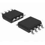
| 封装/外壳 | 8-SOIC(0.154",3.90mm 宽) |
| 封装/箱体 | SOIC-8 |
| 工作温度 | -40°C ~ 85°C |
| 工作温度范围 | - 40 C to + 85 C |
| 工作电源电压 | 2.4 V to 5.25 V |
| 工厂包装数量 | 97 |
| 振荡器类型 | 内部 |
| 接口类型 | I2C, SPI, UART |
| 数据RAM大小 | 256 B |
| 数据Ram类型 | SRAM |
| 数据总线宽度 | 8 bit |
| 数据转换器 | A/D 8x8b |
| 最大工作温度 | + 85 C |
| 最大时钟频率 | 24 MHz |
| 最小工作温度 | - 40 C |
| 标准包装 | 97 |
| 核心 | M8C |
| 核心处理器 | M8C |
| 核心尺寸 | 8-位 |
| 片上ADC | Yes |
| 电压-电源(Vcc/Vdd) | 2.4 V ~ 5.25 V |
| 电源电压-最大 | 5.25 V |
| 电源电压-最小 | 2.4 V |
| 程序存储器大小 | 4 kB |
| 程序存储器类型 | Flash |
| 程序存储容量 | 4KB(4K x 8) |
| 系列 | CY8C21x23 |
| 输入/输出端数量 | 6 I/O |
| 连接性 | I²C, SPI, UART/USART |
| 速度 | 24MHz |
| 配用 | /product-detail/zh/CY3207ISSP/428-1495-ND/573187/product-detail/zh/CY3210-MINIPROG1/428-1585-ND/679696/product-detail/zh/CY3250-21X23QFN-POD/428-1881-ND/1244286/product-detail/zh/CY3250-21X23/428-1886-ND/1244291/product-detail/zh/CY3250-8SOIC-FK/428-1894-ND/1244299/product-detail/zh/CY3250-21X23-POD/428-1904-ND/1244309/product-detail/zh/CY3210-21X23/428-1995-ND/1640226 |
| 长度 | 4.98 mm |
| 高度 | 1.48 mm |


- 商务部:美国ITC正式对集成电路等产品启动337调查
- 曝三星4nm工艺存在良率问题 高通将骁龙8 Gen1或转产台积电
- 太阳诱电将投资9.5亿元在常州建新厂生产MLCC 预计2023年完工
- 英特尔发布欧洲新工厂建设计划 深化IDM 2.0 战略
- 台积电先进制程称霸业界 有大客户加持明年业绩稳了
- 达到5530亿美元!SIA预计今年全球半导体销售额将创下新高
- 英特尔拟将自动驾驶子公司Mobileye上市 估值或超500亿美元
- 三星加码芯片和SET,合并消费电子和移动部门,撤换高东真等 CEO
- 三星电子宣布重大人事变动 还合并消费电子和移动部门
- 海关总署:前11个月进口集成电路产品价值2.52万亿元 增长14.8%


PDF Datasheet 数据手册内容提取
CY8C21123/CY8C21223/CY8C21323 ® PSoC Programmable System-on-Chip™ Features ■Powerful Harvard-architecture processor: ■Additional system resources: ❐M8C processor speeds up to 24 MHz ❐I2C master, slave and multi-master to 400 kHz ❐Low power at high speed ❐Watchdog and sleep timers ❐Operating voltage: 2.4 V to 5.25 V ❐User-configurable low-voltage detection (LVD) ❐Operating voltages down to 1.0 V using on-chip switch mode ❐Integrated supervisory circuit pump (SMP) ❐On-chip precision voltage reference ❐Industrial temperature range: –40 °C to +85 °C ■Advanced peripherals (PSoC® blocks): ❐Four analog type “E” PSoC blocks provide: Logic Block Diagram • Two comparators with digital to analog converter (DAC) references • Single or dual 10-Bit 8-to-1 analog to digital converter Port 1 Port 0 (ADC) PSoC ❐Four digital PSoC blocks provide: CORE • 8- to 32-bit timers and counters, 8- and 16-bit pulse-width modulators (PWMs) System Bus • CRC and PRS modules ❐Full duplex UART, SPI master or slave: Connectable to all Global Digital Interconnect general-purpose I/O (GPIO) pins Global Analog Interconnect ❐Complex peripherals by combining blocks SRAM SROM Flash ■Flexible on-chip memory: CPU Core Sleep and ❐4 KB flash program storage 50,000 erase/write cycles Interrupt (M8C) Watchdog Controller ❐256 bytes SRAM data storage ❐In-system serial programming (ISSP) Clock Sources ❐Partial flash updates (Includes IMO and ILO) ❐Flexible protection modes ❐EEPROM emulation in flash DIGITAL SYSTEM ANALOG SYSTEM ■Complete development tools: Analog Ref. ❐Free development software (PSoC Designer™) Digital Analog PSoC Block PSoC Block ❐Full-featured, in-circuit emulator (ICE) and programmer Array Array ❐Full-speed emulation ❐Complex breakpoint structure ❐128-KB trace memory ■Precision, programmable clocking: ❐Internal ±5% 24- / 48-MHz main oscillator ❐Internal low-speed, low-power oscillator for watchdog and POR and LVD Switch Internal sleep functionality Digital I2C Mode Voltage Clocks System Resets Pump Ref. ■Programmable pin configurations: SYSTEM RESOURCES ❐25-mA sink, 10-mA source on all GPIOs ❐Pull-up, pull-down, high Z, strong, or open-drain drive modes on all GPIOs ❐Up to eight analog inputs on all GPIOs ❐Configurable interrupt on all GPIOs ■ Errata: When the device is operated within 0 °C to 70 °C, the frequency tolerance is reduced to ±2.5%, but if operated at extreme temperature (below 0 °C or above 70°C), frequency tolerance deviates from ±2.5% to ±5%. For information on silicon errata, see “Errata” on page43. CypressSemiconductorCorporation • 198 Champion Court • SanJose, CA 95134-1709 • 408-943-2600 Document Number: 38-12022 Rev. AC Revised November 22, 2017
CY8C21123/CY8C21223/CY8C21323 Contents PSoC Functional Overview ..............................................3 Absolute Maximum Ratings .......................................16 PSoC Core ..................................................................3 Operating Temperature ............................................17 Digital System .............................................................3 DC Electrical Characteristics .....................................17 Analog System ............................................................4 AC Electrical Characteristics .....................................23 Additional System Resources .....................................4 Packaging Information ...................................................31 PSoC Device Characteristics ......................................5 Packaging Dimensions ..............................................31 Getting Started ..................................................................5 Thermal Impedances ................................................35 Application Notes ........................................................5 Solder Reflow Specifications .....................................35 Development Kits ........................................................5 Ordering Information ......................................................36 Training .......................................................................5 Ordering Code Definitions ........................................36 CYPros Consultants ....................................................5 Acronyms ........................................................................37 Solutions Library ..........................................................5 Acronyms Used .........................................................37 Technical Support .......................................................5 Reference Documents ....................................................37 Development Tool Selection ...........................................6 Document Conventions .................................................38 Software ......................................................................6 Units of Measure .......................................................38 Designing with PSoC Designer .......................................7 Numeric Conventions ................................................38 Select Components .....................................................7 Glossary ..........................................................................38 Configure Components ...............................................7 Errata ...............................................................................43 Organize and Connect ................................................7 Part Numbers Affected ..............................................43 Generate, Verify, and Debug .......................................7 CY8C21123 Qualification Status ...............................43 Pin Information .................................................................8 CY8C21123 Errata Summary ....................................43 8-Pin Part Pinout .........................................................8 Document History Page .................................................44 16-Pin Part Pinout .......................................................8 Sales, Solutions, and Legal Information ......................47 20-Pin Part Pinout .....................................................10 Worldwide Sales and Design Support .......................47 24-Pin Part Pinout .....................................................11 Products ....................................................................47 Register Reference .........................................................12 PSoC® Solutions .......................................................47 Register Conventions ................................................12 Cypress Developer Community .................................47 Register Mapping Tables ..........................................12 Technical Support .....................................................47 Electrical Specifications ................................................16 Document Number: 38-12022 Rev. AC Page 2 of 47
CY8C21123/CY8C21223/CY8C21323 PSoC Functional Overview The PSoC family consists of many programmable Digital System system-on-chip controller devices. These devices are designed The digital system consists of four digital PSoC blocks. Each to replace multiple traditional MCU-based system components block is an 8-bit resource that can be used alone or combined with a low cost single-chip programmable component. A PSoC with other blocks to form 8, 16, 24, and 32-bit peripherals, which device includes configurable blocks of analog and digital logic, are called user modules. Digital peripheral configurations and programmable interconnect. This architecture allows you to include: create customized peripheral configurations, to match the requirements of each individual application. Additionally, a fast ■PWMs (8- and 16-bit) CPU, Flash program memory, SRAM data memory, and configurable I/O are included in a range of convenient pinouts. ■PWMs with dead band (8- and 16-bit) The PSoC architecture, as shown in Figure1, consists of four ■Counters (8- to 32-bit) main areas: the Core, the System Resources, the Digital ■Timers (8- to 32-bit) System, and the Analog System. Configurable global bus resources allow the combining of all device resources into a ■UART 8-bit with selectable parity (up to two) complete custom system. Each PSoC device includes four digital blocks. Depending on the PSoC package, up to two analog ■SPI master and slave comparators and up to 16 GPIO are also included. The GPIO ■I2C slave, master, multi-master (one available as a system provide access to the global digital and analog interconnects. resource) PSoC Core ■Cyclical redundancy checker/generator (8-bit) The PSoC Core is a powerful engine that supports a rich ■IrDA (up to two) instruction set. It encompasses SRAM for data storage, an interrupt controller, sleep and watchdog timers, and internal main ■Pseudo random sequence generators (8- to 32-bit) oscillator (IMO), and internal low-speed oscillator (ILO). The The digital blocks can be connected to any GPIO through a CPU core, called the M8C, is a powerful processor with speeds series of global bus that can route any signal to any pin. The up to 24 MHz. The M8C is a four MIPS 8-bit Harvard-architecture busses also allow for signal multiplexing and performing logic microprocessor. operations. This configurability frees your designs from the System Resources provide additional capability, such as digital constraints of a fixed peripheral controller. clocks or I2C functionality for implementing an I2C master, slave, Digital blocks are provided in rows of four, where the number of MultiMaster, an internal voltage reference that provides an blocks varies by PSoC device family. This provides an optimum absolute value of 1.3 V to a number of PSoC subsystems, an choice of system resources for your application. Family SMP that generates normal operating voltages off a single resources are shown in Table 1 on page 5. battery cell, and various system resets supported by the M8C. Figure 1. Digital System Block Diagram The digital system consists of an array of digital PSoC blocks, which can be configured into any number of digital peripherals. Port 1 The digital blocks can be connected to the GPIO through a series Port 0 of global bus that can route any signal to any pin. This frees designs from the constraints of a fixed peripheral controller. Digital Clocks To System Bus To Analog The analog system consists of four analog PSoC blocks, From Core System supporting comparators and analog-to-digital conversion up to 10 bits of precision. DIGITAL SYSTEM Digital PSoC Block Array Row InputConfiguration DBB00 DBB0R1owD 0CB02 DCB0344 ConfigurationRow Output 8 8 8 8 Global Digital GIE[7:0] Interconnect GOE[7:0] GIO[7:0] GOO[7:0] Document Number: 38-12022 Rev. AC Page 3 of 47
CY8C21123/CY8C21223/CY8C21323 Analog System Additional System Resources The analog system consists of four configurable blocks to allow System resources, some of which listed in the previous sections, creation of complex analog signal flows. Analog peripherals are provide additional capability useful to complete systems. very flexible and may be customized to support specific Additional resources include a switch mode pump, low voltage application requirements. Some of the more common PSoC detection, and power on reset. The merits of each system analog functions (most available as user modules) are: resource are. ■Analog-to-digital converters (single or dual, with 8-bit or 10-bit ■Digital clock dividers provide three customizable clock resolution) frequencies for use in applications. The clocks can be routed to both the digital and analog systems. Additional clocks can ■Pin-to-pin comparators (one) be generated using digital PSoC blocks as clock dividers. ■Single-ended comparators (up to 2) with absolute (1.3 V) ■The I2C module provides 100 and 400 kHz communication over reference or 8-bit DAC reference two wires. Slave, master, and multi-master modes are all ■1.3 V reference (as a system resource) supported. In most PSoC devices, analog blocks are provided in columns of ■LVD interrupts can signal the application of falling voltage three, which includes one CT (continuous time) and two SC levels, while the advanced POR (power on reset) circuit (switched capacitor) blocks. The CY8C21x23 devices provide eliminates the need for a system supervisor. limited functionality Type “E” analog blocks. Each column ■An internal 1.3 V voltage reference provides an absolute contains one CT block and one SC block. reference for the analog system, including ADCs and DACs. The number of blocks on the device family is listed in Table 1 on page 5. ■An integrated switch mode pump (SMP) generates normal operating voltages from a single 1.2 V battery cell, providing a Figure 2. CY8C21x23 Analog System Block Diagram low cost boost converter. Array Input Configuration ACI0[1:0] ACI1[1:0] ACOL1MUX Array ACE00 ACE01 ASE10 ASE11 Document Number: 38-12022 Rev. AC Page 4 of 47
CY8C21123/CY8C21223/CY8C21323 PSoC Device Characteristics Depending on your PSoC device characteristics, the digital and analog systems can have 16, 8, or 4 digital blocks, and 12, 6, or 4 analog blocks. Table1 lists the resources available for specific PSoC device groups. The PSoC device covered by this datasheet is highlighted. Table 1. PSoC Device Characteristics PSoC Part Digital Digital Digital Analog Analog Analog Analog SRAM Flash Number I/O Rows Blocks Inputs Outputs Columns Blocks Size Size CY8C29x66 up to 64 4 16 up to 12 4 4 12 2 K 32 K CY8C28xxx up to 44 up to 3 up to 12 up to 44 up to 4 up to 6 up to 1 K 16 K 12 + 4[1] CY8C27x43 up to 44 2 8 up to 12 4 4 12 256 16 K CY8C24x94 up to 56 1 4 up to 48 2 2 6 1 K 16 K CY8C24x23A up to 24 1 4 up to 12 2 2 6 256 4 K CY8C23x33 up to 26 1 4 up to 12 2 2 4 256 8 K CY8C22x45 up to 38 2 8 up to 38 0 4 6[1] 1 K 16 K CY8C21x45 up to 24 1 4 up to 24 0 4 6[1] 512 8 K CY8C21x34 up to 28 1 4 up to 28 0 2 4[1] 512 8 K CY8C21x23 up to 16 1 4 up to 8 0 2 4[1] 256 4 K CY8C20x34 up to 28 0 0 up to 28 0 0 3[1,2] 512 8 K CY8C20xx6 up to 36 0 0 up to 36 0 0 3[1,2] up to up to 2 K 32 K Getting Started The quickest way to understand PSoC silicon is to read this Training datasheet and then use the PSoC Designer Integrated Devel- Free PSoC technical training (on demand, webinars, and opment Environment (IDE). This datasheet is an overview of the workshops) is available online at http://www.cypress.com. The PSoC integrated circuit and presents specific pin, register, and training covers a wide variety of topics and skill levels to assist electrical specifications. you in your designs. For in depth information, along with detailed programming details, see the Technical Reference Manual for this PSoC CYPros Consultants device. Certified PSoC Consultants offer everything from technical For up to date ordering, packaging, and electrical specification assistance to completed PSoC designs. To contact or become a information, see the latest PSoC device datasheets on the web PSoC Consultant go to http://www.cypress.com and refer to at http://www.cypress.com. CYPros Consultants. Application Notes Solutions Library Application notes are an excellent introduction to the wide variety Visit our growing library of solution focused designs at of possible PSoC designs. They can be found at http://www.cypress.com. Here you can find various application http://www.cypress.com. designs that include firmware and hardware design files that enable you to complete your designs quickly. Development Kits Technical Support PSoC Development Kits are available online from Cypress at http://www.cypress.com and through a growing number of For assistance with technical issues, search KnowledgeBase regional and global distributors, which include Arrow, Avnet, articles and forums at http://www.cypress.com. If you cannot find Digi-Key, Farnell, Future Electronics, and Newark. an answer to your question, call technical support at 1-800-541-4736. Notes 1. Limited analog functionality. 2. Two analog blocks and one CapSense®. Document Number: 38-12022 Rev. AC Page 5 of 47
CY8C21123/CY8C21223/CY8C21323 Development Tool Selection Software Debugger PSoC Designer has a debug environment that provides PSoC Designer hardware in-circuit emulation, allowing you to test the program in At the core of the PSoC development software suite is a physical system while providing an internal view of the PSoC PSoCDesigner. Utilized by thousands of PSoC developers, this device. Debugger commands allow the designer to read and robust software has been facilitating PSoC designs for years. program and read and write data memory, read and write I/O PSoCDesigner is available free of charge at registers, read and write CPU registers, set and clear break- http://www.cypress.com. PSoC Designer comes with a free C points, and provide program run, halt, and step control. The compiler. debugger also allows the designer to create a trace buffer of registers and memory locations of interest. PSoC Designer Software Subsystems You choose a base device to work with and then select different In-Circuit Emulator onboard analog and digital components called user modules that A low cost, high functionality In-Circuit Emulator (ICE) is use the PSoC blocks. Examples of user modules are ADCs, available for development support. This hardware has the DACs, Amplifiers, and Filters. You configure the user modules capability to program single devices. The emulator consists of a for your chosen application and connect them to each other and base unit that connects to the PC by way of a USB port. The base to the proper pins. Then you generate your project. This prepop- unit is universal and operates with all PSoC devices. Emulation ulates your project with APIs and libraries that you can use to pods for each device family are available separately. The program your application. emulation pod takes the place of the PSoC device in the target The tool also supports easy development of multiple configura- board and performs full speed (24MHz) operation. tions and dynamic reconfiguration. Dynamic reconfiguration Standard Cypress PSoC IDE tools are available for debugging allows for changing configurations at run time. Code Generation the CY8C20x36A/66A family of parts. However, the additional Tools PSoC Designer supports multiple third-party C compilers trace length and a minimal ground plane in the Flex-Pod can and assemblers. The code generation tools work seamlessly create noise problems that make it difficult to debug the design. within the PSoC Designer interface and have been tested with a A custom bonded On-Chip Debug (OCD) device is available in a full range of debugging tools. The choice is yours. 48-pin QFN package. The OCD device is recommended for debugging designs that have high current and/or high analog Assemblers. The assemblers allow assembly code to be accuracy requirements. The QFN package is compact and is merged seamlessly with C code. Link libraries automatically use connected to the ICE through a high density connector. absolute addressing or are compiled in relative mode, and linked with other software modules to get absolute addressing. PSoC Programmer Flexible enough to be used on the bench in development, yet C Language Compilers. C language compilers are available suitable for factory programming, PSoC Programmer works that support the PSoC family of devices. The products allow you either as a standalone programming application or it can operate to create complete C programs for the PSoC family devices. The directly from PSoC Designer. PSoC Programmer software is optimizing C compilers provide all the features of C tailored to compatible with both PSoC ICE-Cube in-circuit emulator and the PSoC architecture. They come complete with embedded PSoC MiniProg. PSoC programmer is available free of charge at libraries providing port and bus operations, standard keypad and http://www.cypress.com/psocprogrammer. display support, and extended math functionality. Document Number: 38-12022 Rev. AC Page 6 of 47
CY8C21123/CY8C21223/CY8C21323 Designing with PSoC Designer The development process for the PSoC device differs from that Organize and Connect of a traditional fixed function microprocessor. The configurable You build signal chains at the chip level by interconnecting user analog and digital hardware blocks give the PSoC architecture a modules to each other and the I/O pins. You perform the unique flexibility that pays dividends in managing specification selection, configuration, and routing so that you have complete change during development and by lowering inventory costs. control over all on-chip resources. These configurable resources, called PSoC Blocks, have the ability to implement a wide variety of user-selectable functions. Generate, Verify, and Debug The PSoC development process can be summarized in the When you are ready to test the hardware configuration or move following four steps: on to developing code for the project, you perform the "Generate 1.Select User Modules Configuration Files" step. This causes PSoC Designer to generate source code that automatically configures the device to 2.Configure User Modules your specification and provides the software for the system. The 3.Organize and Connect generated code provides application programming interfaces 4.Generate, Verify, and Debug (APIs) with high-level functions to control and respond to hardware events at run time and interrupt service routines that Select Components you can adapt as needed. PSoC Designer provides a library of pre-built, pre-tested A complete code development environment allows you to hardware peripheral components called "user modules." User develop and customize your applications in C, assembly modules make selecting and implementing peripheral devices, language, or both. both analog and digital, simple. The last step in the development process takes place inside Configure Components PSoC Designer's Debugger (access by clicking the Connect icon). PSoC Designer downloads the HEX image to the ICE Each of the User Modules you select establishes the basic where it runs at full speed. PSoC Designer debugging capabil- register settings that implement the selected function. They also ities rival those of systems costing many times more. In addition provide parameters and properties that allow you to tailor their precise configuration to your particular application. For example, to traditional single-step, run-to-breakpoint and watch-variable a PWM User Module configures one or more features, the debug interface provides a large trace buffer and allows you to define complex breakpoint events that include digital PSoC blocks, one for each 8 bits of resolution. The user monitoring address and data bus values, memory locations and module parameters permit you to establish the pulse width and external signals. duty cycle. Configure the parameters and properties to corre- spond to your chosen application. Enter values directly or by selecting values from drop-down menus. All the user modules are documented in datasheets that may be viewed directly in PSoC Designer or on the Cypress website. These user module datasheets explain the internal operation of the User Module and provide performance specifications. Each datasheet describes the use of each user module parameter, and other information you may need to successfully implement your design. Document Number: 38-12022 Rev. AC Page 7 of 47
CY8C21123/CY8C21223/CY8C21323 Pin Information This section describes, lists, and illustrates the CY8C21x23 PSoC device pins and pinout configurations. Every port pin (labeled with a “P”) is capable of Digital I/O. However, V , V , SMP, and XRES are not capable of Digital I/O. SS DD 8-Pin Part Pinout Table 2. Pin Definitions – CY8C21123 8-Pin SOIC Pin Type Pin Figure 3. CY8C21123 8-Pin SOIC Description No. Digital Analog Name 1 I/O I P0[5] Analog column mux input A, I, P0[5] 1 8 VDD A, I, P0[3] 2 7 P0[4], A, I 2 I/O I P0[3] Analog column mux input I2C SCL, P1[1] 3SOIC6 P0[2], A, I 3 I/O P1[1] I2C serial clock (SCL), ISSP-SCLK[3] VSS 4 5 P1[0], I2C SDA 4 Power V Ground connection SS 5 I/O P1[0] I2C serial data (SDA), ISSP-SDATA[3] 6 I/O I P0[2] Analog column mux input 7 I/O I P0[4] Analog column mux input 8 Power V Supply voltage DD LEGEND: A = Analog, I = Input, and O = Output. 16-Pin Part Pinout Table 3. Pin Definitions – CY8C21223 16-Pin SOIC Pin Type Pin Figure 4. CY8C21223 16-Pin SOIC Description No. Digital Analog Name 1 I/O I P0[7] Analog column mux input A, I, P0[7] 1 16 VDD A, I, P0[5] 2 15 P0[6], A, I 2 I/O I P0[5] Analog column mux input A, I, P0[3] 3 14 P0[4], A, I 3 I/O I P0[3] Analog column mux input A, I, P0[1] 4 SOIC 13 P0[2], A, I SMP 5 12 P0[0], A, I 4 I/O I P0[1] Analog column mux input VSS 6 11 P1[4], EXTCLK 5 Power SMP SMP connection to required external I2C SCL, P1[1] 7 10 P1[2] components VSS 8 9 P1[0], I2C SDA 6 Power V Ground connection SS 7 I/O P1[1] I2C SCL, ISSP-SCLK[3] 8 Power V Ground connection SS 9 I/O P1[0] I2C SDA, ISSP-SDATA[3] 10 I/O P1[2] 11 I/O P1[4] Optional external clock input (EXTCLK) 12 I/O I P0[0] Analog column mux input 13 I/O I P0[2] Analog column mux input 14 I/O I P0[4] Analog column mux input 15 I/O I P0[6] Analog column mux input 16 Power V Supply voltage DD LEGEND A = Analog, I = Input, and O = Output. Note 3. These are the ISSP pins, which are not high Z at POR (power on reset). See the PSoC Technical Reference Manual for details. Document Number: 38-12022 Rev. AC Page 8 of 47
CY8C21123/CY8C21223/CY8C21323 Table 4. Pin Definitions – CY8C21223 16-Pin QFN with no E-Pad [4] Pin Type Pin Figure 5. CY8C21223 16-Pin QFN Description No. Digital Analog Name AIAI 12 II//OO II PP00[[31]] AAnnaalloogg ccoolluummnn mmuuxx iinnppuutt NCP0[5], P0[7], VDD 3 I/O P1[7] I2C SCL 654 3 4 I/O P1[5] I2C SDA AAII,, PP00[[31]] 1211QF1N 11121 XPR0[E4S], VREF 5 I/O P1[3] I2C SCL, P1[7] 3 (Top View)10 P1[4] 6 I/O P1[1] I2C SCL, ISSP-SCLK[5] I2C SDA, P1[5] 45 6789 P1[6] 7 Power V Ground connection 8 I/O P1SS[0] I2C SDA, ISSP-SDATA[5] 1[3] 1[1]VSS1[0] P P P 9 I/O P1[6] L, A, C D S S 10 I/O P1[4] EXTCLK C C 2 2 11 Input XRES Active high external reset with internal I I pull-down 12 I/O I P0[4] V REF 13 Power V Supply voltage DD 14 I/O I P0[7] Analog column mux input 15 I/O I P0[5] Analog column mux input 16 NC No Connection. Pin must be left floating LEGEND A = Analog, I = Input, and O = Output. Notes 4. The center pad on the QFN package must be connected to ground (Vss) for best mechanical, thermal, and electrical performance. If not connected to ground, it must be electrically floated and not connected to any other signal. 5. These are the ISSP pins, which are not high Z at POR (power on reset). See the PSoC Technical Reference Manual for details. Document Number: 38-12022 Rev. AC Page 9 of 47
CY8C21123/CY8C21223/CY8C21323 20-Pin Part Pinout Table 5. Pin Definitions – CY8C21323 20-Pin SSOP Pin Type Pin Figure 6. CY8C21323 20-Pin SSOP Description No. Digital Analog Name 1 I/O I P0[7] Analog column mux input A, I, P0[7] 1 20 VDD 2 I/O I P0[5] Analog column mux input A, I, P0[5] 2 19 P0[6], A, I A, I, P0[3] 3 18 P0[4], A, I 3 I/O I P0[3] Analog column mux input A, I, P0[1] 4 17 P0[2], A, I 4 I/O I P0[1] Analog column mux input VSS 5 SSOP 16 P0[0], A, I 5 Power V Ground connection[6] I2C SCL, P1[7] 6 15 XRES SS I2C SDA, P1[5] 7 14 P1[6] 6 I/O P1[7] I2C SCL P1[3] 8 13 P1[4], EXTCLK 7 I/O P1[5] I2C SDA I2C SCL, P1[1] 9 12 P1[2] 8 I/O P1[3] VSS 10 11 P1[0], I2C SDA 9 I/O P1[1] I2C SCL, ISSP-SCLK[7] 10 Power V Ground connection[6] SS 11 I/O P1[0] I2C SDA, ISSP-SDATA[7] 12 I/O P1[2] 13 I/O P1[4] Optional EXTCLK input 14 I/O P1[6] 15 Input XRES Active high external reset with internal pull-down 16 I/O I P0[0] Analog column mux input 17 I/O I P0[2] Analog column mux input 18 I/O I P0[4] Analog column mux input 19 I/O I P0[6] Analog column mux input 20 Power V Supply voltage DD LEGEND A = Analog, I = Input, and O = Output. Notes 6. All VSS pins should be brought out to one common GND plane. 7. These are the ISSP pins, which are not high Z at POR (power on reset). See the PSoC Technical Reference Manual for details. Document Number: 38-12022 Rev. AC Page 10 of 47
CY8C21123/CY8C21223/CY8C21323 24-Pin Part Pinout Table 6. Pin Definitions – CY8C21323 24-Pin QFN[8] Pin Type Pin Figure 7. CY8C21323 24-Pin QFN Description No. Digital Analog Name 1 I/O I P0[1] Analog column mux input A, IA, I A, I A, I 2 Power SMP SMP connection to required external P0[3], P0[5], P0[7], VSS VDDP0[6], components 34 I/OPower VP1SS[7] GI2Cro uSnCdL connection[9] A, I, P0[1] 124 232221 201918 P0[4], A, I SMP 2 17 P0[2], A, I 5 I/O P1[5] I2C SDA VSS 3 QFN 16 P0[0], A, I I2C SCL, P1[7] 4 (Top View) 15 NC 6 I/O P1[3] I2C SDA, P1[5] 5 14 XRES 7 I/O P1[1] I2C SCL, ISSP-SCLK[10] P1[3] 6 13 P1[6] 7890 12 1 11 8 NC No connection. Pin must be left floating 91110 II//OOPower VPP11SS[[02]] GI2Cro uSnDdA c, oISnnSePc-tSioDnA[9T]A[10] C SCL, P1[1]NC VSSC SDA, P1[0] P1[2]XTCLK, P1[4] 12 I/O P1[4] Optional (EXTCLK) input I2 I2 E 13 I/O P1[6] 14 Input XRES Active high external reset with internal pull-down 15 NC No connection. Pin must be left floating 16 I/O I P0[0] Analog column mux input 17 I/O I P0[2] Analog column mux input 18 I/O I P0[4] Analog column mux input 19 I/O I P0[6] Analog column mux input 20 Power V Supply voltage DD 21 Power V Ground connection[9] SS 22 I/O I P0[7] Analog column mux input 23 I/O I P0[5] Analog column mux input 24 I/O I P0[3] Analog column mux input LEGEND A = Analog, I = Input, and O = Output. Notes 8. The center pad on the QFN package must be connected to ground (VSS) for best mechanical, thermal, and electrical performance. If not connected to ground, it must be electrically floated and not connected to any other signal. 9. All VSS pins should be brought out to one common GND plane. 10.These are the ISSP pins, which are not high Z at POR (power on reset). See the PSoC Technical Reference Manual for details. Document Number: 38-12022 Rev. AC Page 11 of 47
CY8C21123/CY8C21223/CY8C21323 Register Reference This section lists the registers of the CY8C21x23 PSoC device. Register Mapping Tables For detailed register information, refer the PSoC Technical The PSoC device has a total register address space of Reference Manual. 512 bytes. The register space is referred to as I/O space and is Register Conventions divided into two banks. The XOI bit in the Flag register (CPU_F) determines the bank you are currently in. When the XOI bit is set, The register conventions specific to this section are listed in you are in Bank 1. Table7. Note In the following register mapping tables, blank fields are Table 7. Register Conventions Reserved and must not be accessed. Convention Description R Read register or bit(s) W Write register or bit(s) L Logical register or bit(s) C Clearable register or bit(s) # Access is bit specific Document Number: 38-12022 Rev. AC Page 12 of 47
CY8C21123/CY8C21223/CY8C21323 Table 8. Register Map Bank 0 Table: User Space Addr Addr Addr Addr Name Access Name Access Name Access Name Access (0,Hex) (0,Hex) (0,Hex) (0,Hex) PRT0DR 00 RW 40 ASE10CR0 80 RW C0 PRT0IE 01 RW 41 81 C1 PRT0GS 02 RW 42 82 C2 PRT0DM2 03 RW 43 83 C3 PRT1DR 04 RW 44 ASE11CR0 84 RW C4 PRT1IE 05 RW 45 85 C5 PRT1GS 06 RW 46 86 C6 PRT1DM2 07 RW 47 87 C7 08 48 88 C8 09 49 89 C9 0A 4A 8A CA 0B 4B 8B CB 0C 4C 8C CC 0D 4D 8D CD 0E 4E 8E CE 0F 4F 8F CF 10 50 90 D0 11 51 91 D1 12 52 92 D2 13 53 93 D3 14 54 94 D4 15 55 95 D5 16 56 96 I2C_CFG D6 RW 17 57 97 I2C_SCR D7 # 18 58 98 I2C_DR D8 RW 19 59 99 I2C_MSCR D9 # 1A 5A 9A INT_CLR0 DA RW 1B 5B 9B INT_CLR1 DB RW 1C 5C 9C DC 1D 5D 9D INT_CLR3 DD RW 1E 5E 9E INT_MSK3 DE RW 1F 5F 9F DF DBB00DR0 20 # AMX_IN 60 RW A0 INT_MSK0 E0 RW DBB00DR1 21 W 61 A1 INT_MSK1 E1 RW DBB00DR2 22 RW PWM_CR 62 RW A2 INT_VC E2 RC DBB00CR0 23 # 63 A3 RES_WDT E3 W DBB01DR0 24 # CMP_CR0 64 # A4 E4 DBB01DR1 25 W 65 A5 E5 DBB01DR2 26 RW CMP_CR1 66 RW A6 DEC_CR0 E6 RW DBB01CR0 27 # 67 A7 DEC_CR1 E7 RW DCB02DR0 28 # ADC0_CR 68 # A8 E8 DCB02DR1 29 W ADC1_CR 69 # A9 E9 DCB02DR2 2A RW 6A AA EA DCB02CR0 2B # 6B AB EB DCB03DR0 2C # TMP_DR0 6C RW AC EC DCB03DR1 2D W TMP_DR1 6D RW AD ED DCB03DR2 2E RW TMP_DR2 6E RW AE EE DCB03CR0 2F # TMP_DR3 6F RW AF EF Blank fields are Reserved and must not be accessed. # Access is bit specific. Document Number: 38-12022 Rev. AC Page 13 of 47
CY8C21123/CY8C21223/CY8C21323 Table 8. Register Map Bank 0 Table: User Space (continued) Addr Addr Addr Addr Name Access Name Access Name Access Name Access (0,Hex) (0,Hex) (0,Hex) (0,Hex) 30 70 RDI0RI B0 RW F0 31 71 RDI0SYN B1 RW F1 32 ACE00CR1 72 RW RDI0IS B2 RW F2 33 ACE00CR2 73 RW RDI0LT0 B3 RW F3 34 74 RDI0LT1 B4 RW F4 35 75 RDI0RO0 B5 RW F5 36 ACE01CR1 76 RW RDI0RO1 B6 RW F6 37 ACE01CR2 77 RW B7 CPU_F F7 RL 38 78 B8 F8 39 79 B9 F9 3A 7A BA FA 3B 7B BB FB 3C 7C BC FC 3D 7D BD FD 3E 7E BE CPU_SCR1 FE # 3F 7F BF CPU_SCR0 FF # Blank fields are Reserved and must not be accessed. # Access is bit specific. Table 9. Register Map Bank 1 Table: Configuration Space Addr Addr Addr Addr Name Access Name Access Name Access Name Access (1,Hex) (1,Hex) (1,Hex) (1,Hex) PRT0DM0 00 RW 40 ASE10CR0 80 RW C0 PRT0DM1 01 RW 41 81 C1 PRT0IC0 02 RW 42 82 C2 PRT0IC1 03 RW 43 83 C3 PRT1DM0 04 RW 44 ASE11CR0 84 RW C4 PRT1DM1 05 RW 45 85 C5 PRT1IC0 06 RW 46 86 C6 PRT1IC1 07 RW 47 87 C7 08 48 88 C8 09 49 89 C9 0A 4A 8A CA 0B 4B 8B CB 0C 4C 8C CC 0D 4D 8D CD 0E 4E 8E CE 0F 4F 8F CF 10 50 90 GDI_O_IN D0 RW 11 51 91 GDI_E_IN D1 RW 12 52 92 GDI_O_OU D2 RW 13 53 93 GDI_E_OU D3 RW 14 54 94 D4 15 55 95 D5 16 56 96 D6 17 57 97 D7 18 58 98 D8 19 59 99 D9 1A 5A 9A DA 1B 5B 9B DB Blank fields are Reserved and must not be accessed. # Access is bit specific. Document Number: 38-12022 Rev. AC Page 14 of 47
CY8C21123/CY8C21223/CY8C21323 Table 9. Register Map Bank 1 Table: Configuration Space (continued) Addr Addr Addr Addr Name Access Name Access Name Access Name Access (1,Hex) (1,Hex) (1,Hex) (1,Hex) 1C 5C 9C DC 1D 5D 9D OSC_GO_EN DD RW 1E 5E 9E OSC_CR4 DE RW 1F 5F 9F OSC_CR3 DF RW DBB00FN 20 RW CLK_CR0 60 RW A0 OSC_CR0 E0 RW DBB00IN 21 RW CLK_CR1 61 RW A1 OSC_CR1 E1 RW DBB00OU 22 RW ABF_CR0 62 RW A2 OSC_CR2 E2 RW 23 AMD_CR0 63 RW A3 VLT_CR E3 RW DBB01FN 24 RW CMP_GO_EN 64 RW A4 VLT_CMP E4 R DBB01IN 25 RW 65 A5 ADC0_TR E5 RW DBB01OU 26 RW AMD_CR1 66 RW A6 ADC1_TR E6 RW 27 ALT_CR0 67 RW A7 E7 DCB02FN 28 RW 68 A8 IMO_TR E8 W DCB02IN 29 RW 69 A9 ILO_TR E9 W DCB02OU 2A RW 6A AA BDG_TR EA RW 2B CLK_CR3 6B RW AB ECO_TR EB W DCB03FN 2C RW TMP_DR0 6C RW AC EC DCB03IN 2D RW TMP_DR1 6D RW AD ED DCB03OU 2E RW TMP_DR2 6E RW AE EE 2F TMP_DR3 6F RW AF EF 30 70 RDI0RI B0 RW F0 31 71 RDI0SYN B1 RW F1 32 ACE00CR1 72 RW RDI0IS B2 RW F2 33 ACE00CR2 73 RW RDI0LT0 B3 RW F3 34 74 RDI0LT1 B4 RW F4 35 75 RDI0RO0 B5 RW F5 36 ACE01CR1 76 RW RDI0RO1 B6 RW F6 37 ACE01CR2 77 RW B7 CPU_F F7 RL 38 78 B8 F8 39 79 B9 F9 3A 7A BA FLS_PR1 FA RW 3B 7B BB FB 3C 7C BC FC 3D 7D BD FD 3E 7E BE CPU_SCR1 FE # 3F 7F BF CPU_SCR0 FF # Blank fields are Reserved and must not be accessed. # Access is bit specific. Document Number: 38-12022 Rev. AC Page 15 of 47
CY8C21123/CY8C21223/CY8C21323 Electrical Specifications This section presents the DC and AC electrical specifications of the CY8C21x23 PSoC device. For up to date electrical specifications, check if you have the latest datasheet by visiting the web at http://www.cypress.com. Specifications are valid for –40 °C T 85 °C and T 100 °C, except where noted. A J Refer to Table 24 on page 25 for the electrical specifications on the IMO using SLIMO mode. Figure 10. Voltage versus CPU Frequency Figure 11. Voltage versus IMO Frequency 5.25 5.25 0 S= LIMO SLIMO e Mdode=1 Mode=0 o 4.75 O V 4.75 M oltage Regpieornatianligd dd Voltage SLIMO V V d 3.60 d SLIMO SLIMO V Mode=1 Mode=0 3.00 3.00 SLIMO SLIMO Mode=1Mode=1 2.40 2.40 93 kHz 3 MHz 12 MHz 24 MHz 93 kHz 6 MHz 12 MHz 24 MHz CPU Frequency IMO Frequency Absolute Maximum Ratings Exceeding maximum ratings may shorten the useful life of the device. User guidelines are not tested. Table 10. Absolute Maximum Ratings Symbol Description Min Typ Max Units Notes Higher storage temperatures reduce data retention time. Recommended storage T Storage temperature –55 – +100 °C temperature is +25 °C ± 25 °C. STG Extended duration storage temperatures higher than 65 °C degrade reliability. See T Bake temperature – 125 package °C BAKETEMP label See t Bake time package – 72 Hours BAKETIME label T Ambient temperature with power applied –40 – +85 °C A V Supply voltage on V relative to V –0.5 – +6.0 V DD DD SS V DC input voltage V – 0.5 – V + 0.5 V IO SS DD V DC voltage applied to tristate V – 0.5 – V + 0.5 V IOZ SS DD I Maximum current into any port pin –25 – +50 mA MIO ESD Electro static discharge voltage 2000 – – V Human body model ESD LU Latch-up current – – 200 mA Document Number: 38-12022 Rev. AC Page 16 of 47
CY8C21123/CY8C21223/CY8C21323 Operating Temperature Table 11. Operating Temperature Symbol Description Min Typ Max Units Notes T Ambient temperature –40 – +85 °C A The temperature rise from ambient to junction is package specific. See Table 36 on page T Junction temperature –40 – +100 °C J 35. You must limit the power consumption to comply with this requirement. DC Electrical Characteristics DC Chip-Level Specifications Table12 lists the guaranteed maximum and minimum specifications for the voltage and temperature ranges: 4.75 V to 5.25 V and – 40 °C T 85 °C, 3.0 V to 3.6 V and –40 °C T 85 °C, or 2.4 V to 3.0 V and –40 °C T 85 °C, respectively. Typical parameters A A A apply to 5 V, 3.3 V, or 2.7 V at 25 °C and are for design guidance only. Table 12. DC Chip-Level Specifications Symbol Description Min Typ Max Units Notes See DC POR and LVD V Supply voltage 2.40 – 5.25 V specifications, DD Table 19 on page 21. Conditions are V = 5.0 V, DD 25 °C, CPU = 3 MHz, SYSCLK I Supply current, IMO = 24 MHz – 3 4 mA doubler disabled. VC1 = 1.5 MHz DD VC2 = 93.75 kHz VC3 = 0.366 kHz Conditions are V = 3.3 V, DD 25 °C, CPU = 3 MHz, clock doubler I Supply current, IMO = 6 MHz – 1.2 2 mA disabled. VC1 = 375 kHz DD3 VC2 = 23.4 kHz VC3 = 0.091 kHz Conditions are V = 2.55 V, DD 25 °C, CPU = 3 MHz, clock doubler I Supply current, IMO = 6 MHz – 1.1 1.5 mA disabled. VC1 = 375 kHz VC2 = DD27 23.4 kHz VC3 = 0.091 kHz Sleep (mode) current with POR, LVD, sleep I timer, WDT, and internal slow – 2.6 4 µA V = 2.55 V, 0 °C to 40 °C SB27 DD oscillator active. Mid temperature range. Sleep (mode) current with POR, LVD, sleep I timer, WDT, and internal slow – 2.8 5 µA V = 3.3 V, –40 °C T 85 °C SB DD A oscillator active. Trimmed for appropriate V . V V Reference voltage (bandgap) 1.28 1.30 1.32 V DD DD REF = 3.0 V to 5.25 V Trimmed for appropriate V . V V Reference voltage (bandgap) 1.16 1.30 1.330 V DD DD REF27 = 2.4 V to 3.0 V AGND Analog ground V – 0.003 V V + 0.003 V REF REF REF Document Number: 38-12022 Rev. AC Page 17 of 47
CY8C21123/CY8C21223/CY8C21323 DC GPIO Specifications Table13 lists the guaranteed maximum and minimum specifications for the voltage and temperature ranges: 4.75 V to 5.25 V and – 40 °C T 85 °C, 3.0 V to 3.6 V and –40 °C T 85 °C, respectively. Typical parameters apply to 5 V, 3.3 V, or 2.7 V at 25 °C and A A are for design guidance only. Table 13. 5-V and 3.3-V DC GPIO Specifications Symbol Description Min Typ Max Units Notes R Pull-up resistor 4 5.6 8 k PU R Pull-down resistor 4 5.6 8 k PD I = 10 mA, V = 4.75 to 5.25 V (8 total OH DD loads, 4 on even port pins (for example, V High output level V – 1.0 – – V P0[2], P1[4]), 4 on odd port pins (for OH DD example, P0[3], P1[5])). 80 mA maximum combined I budget. OH I = 25 mA, V = 4.75 to 5.25 V (8 total OL DD loads, 4 on even port pins (for example, V Low output level – – 0.75 V P0[2], P1[4]), 4 on odd port pins (for OL example, P0[3], P1[5])). 150 mA maximum combined I budget. OL V = V – 1.0 V, see the limitations of the I High level source current 10 – – mA OH DD OH total current in the note for V . OH V = 0.75 V, see the limitations of the total I Low level sink current 25 – – mA OL OL current in the note for V OL V Input low level – – 0.8 V V = 3.0 to 5.25 IL DD V Input high level 2.1 – V V = 3.0 to 5.25 IH DD V Input hysteresis – 60 – mV H I Input leakage (absolute value) – 1 – nA Gross tested to 1 µA IL Package and pin dependent. C Capacitive load on pins as input – 3.5 10 pF IN Temp = 25 °C Package and pin dependent. C Capacitive load on pins as output – 3.5 10 pF OUT Temp = 25 °C Table14 lists the guaranteed maximum and minimum specifications for the voltage and temperature ranges: 2.4 V to 3.0 V and –40 °C T 85 °C. Typical parameters apply to 2.7 V at 25 °C and are for design guidance only. A Table 14. 2.7-V DC GPIO Specifications Symbol Description Min Typ Max Units Notes R Pull-up resistor 4 5.6 8 k PU R Pull-down resistor 4 5.6 8 k PD I = 2.5 mA (6.25 Typ), V = 2.4 to OH DD V High output level V – 0.4 – – V 3.0 V (16 mA maximum, 50 mA Typ OH DD combined I budget). OH I = 10 mA, V = 2.4 to 3.0 V (90 mA V Low output level – – 0.75 V OL DD OL maximum combined I budget). OL V = V – 0.4 V, see the limitations of the I High level source current 2.5 – – mA OH DD OH total current in the note for V . OH V = 0.75 V, see the limitations of the total I Low level sink current 10 – – mA OL OL current in the note for V . OL V Input low level – – 0.75 V V = 2.4 to 3.0 IL DD V Input high level 2.0 – – V V = 2.4 to 3.0 IH DD V Input hysteresis – 60 – mV H I Input leakage (absolute value) – 1 – nA Gross tested to 1 µA IL Package and pin dependent. C Capacitive load on pins as input – 3.5 10 pF IN Temp = 25 °C Package and pin dependent. C Capacitive load on pins as output – 3.5 10 pF OUT Temp = 25 °C Document Number: 38-12022 Rev. AC Page 18 of 47
CY8C21123/CY8C21223/CY8C21323 DC Amplifier Specifications The following tables list the guaranteed maximum and minimum specifications for the voltage and temperature ranges: 4.75 V to 5.25 V and –40 °C T 85 °C, 3.0 V to 3.6 V and –40 °C T 85 °C, or 2.4 V to 3.0 V and –40 °C T 85 °C, respectively. A A A Typical parameters apply to 5 V, 3.3 V, or 2.7 V at 25 °C and are for design guidance only. Table 15. 5-V DC Amplifier Specifications Symbol Description Min Typ Max Units Notes V Input offset voltage (absolute value) – 2.5 15 mV OSOA TCV Average input offset voltage drift – 10 – µV/°C OSOA I Input leakage current (port 0 analog pins) – 200 – pA Gross tested to 1 µA EBOA Package and pin dependent. C Input capacitance (port 0 analog pins) – 4.5 9.5 pF INOA Temp = 25 °C 0.0 – V Common mode voltage range V – 1 V CMOA DD G Open loop gain 80 – – dB OLOA I Amplifier supply current – 10 30 µA SOA Table 16. 3.3-V DC Amplifier Specifications Symbol Description Min Typ Max Units Notes V Input offset voltage (absolute value) – 2.5 15 mV OSOA TCV Average input offset voltage drift – 10 – µV/°C OSOA I Input leakage current (port 0 analog pins) – 200 – pA Gross tested to 1 µA EBOA Package and pin dependent. C Input capacitance (port 0 analog pins) – 4.5 9.5 pF INOA Temp = 25 °C V Common mode voltage range 0 – V – 1 V CMOA DD G Open loop gain 80 – – dB OLOA I Amplifier supply current – 10 30 µA SOA Table 17. 2.7V DC Amplifier Specifications Symbol Description Min Typ Max Units Notes V Input offset voltage (absolute value) – 2.5 15 mV OSOA TCV Average input offset voltage drift – 10 – µV/°C OSOA I Input leakage current (port 0 analog pins) – 200 – pA Gross tested to 1 µA EBOA Package and pin dependent. C Input capacitance (port 0 analog pins) – 4.5 9.5 pF INOA Temp = 25 °C V Common mode voltage range 0 – V – 1 V CMOA DD G Open loop gain 80 – – dB OLOA I Amplifier supply current – 10 30 µA SOA Document Number: 38-12022 Rev. AC Page 19 of 47
CY8C21123/CY8C21223/CY8C21323 DC Switch Mode Pump Specifications Table18 lists the guaranteed maximum and minimum specifications for the voltage and temperature ranges: 4.75 V to 5.25 V and – 40 °C T 85 °C, 3.0 V to 3.6 V and –40 °C T 85 °C, or 2.4 V to 3.0 V and –40 °C T 85 °C, respectively. Typical parameters A A A apply to 5 V, 3.3 V, or 2.7 V at 25 °C and are for design guidance only. Table 18. DC Switch Mode Pump (SMP) Specifications Symbol Description Min Typ Max Units Notes Configuration of footnote.[11] Average, V 5 V output voltage from pump 4.75 5.0 5.25 V neglecting ripple. SMP trip voltage is set to PUMP5V 5.0 V. Configuration of footnote.[11] Average, V 3.3 V output voltage from pump 3.00 3.25 3.60 V neglecting ripple. SMP trip voltage is set to PUMP3V 3.25 V. Configuration of footnote.[11] Average, V 2.6 V output voltage from pump 2.45 2.55 2.80 V neglecting ripple. SMP trip voltage is set to PUMP2V 2.55 V. Available output current Configuration of footnote.[11] V = 1.8 V, V = 5.0 V 5 – – mA SMP trip voltage is set to 5.0 V. I BAT PUMP PUMP V = 1.5 V, V = 3.25 V 8 – – mA SMP trip voltage is set to 3.25 V. BAT PUMP V = 1.3 V, V = 2.55 V 8 – – mA SMP trip voltage is set to 2.55 V. BAT PUMP Configuration of footnote.[11] SMP trip V Input voltage range from battery 1.8 – 5.0 V BAT5V voltage is set to 5.0 V. Configuration of footnote.[11] SMP trip V Input voltage range from battery 1.0 – 3.3 V BAT3V voltage is set to 3.25 V. Configuration of footnote.[11] SMP trip V Input voltage range from battery 1.0 – 2.8 V BAT2V voltage is set to 2.55 V. Minimum input voltage from battery to start Configuration of footnote.[11] 0 °C T VBATSTART pump 1.2 – – V 100. 1.25 V at T = –40 °C. A A Configuration of footnote.[11] V is the O “V Value for PUMP Trip” specified by the V Line regulation (over Vi range) – 5 – %V DD PUMP_Line O VM[2:0] setting in the DC POR and LVD Specification, Table 19 on page 21. Configuration of footnote.[11] V is the O “V Value for PUMP Trip” specified by the V Load regulation – 5 – %V DD PUMP_Load O VM[2:0] setting in the DC POR and LVD Specification, Table 19 on page 21. Configuration of footnote.[11] Load is V Output voltage ripple (depends on cap/load) – 100 – mVpp PUMP_Ripple 5 mA. Configuration of footnote.[11] Load is E Efficiency 35 50 – % 3 5 mA. SMP trip voltage is set to 3.25 V. For I load = 1 mA, V = 2.55 V, PUMP E Efficiency 35 80 – % V = 1.3 V, 10 uH inductor, 1 uF 2 BAT capacitor, and Schottky diode. F Switching frequency – 1.3 – MHz PUMP DC Switching duty cycle – 50 – % PUMP Note 11.L1 = 2 mH inductor, C1 = 10 mF capacitor, D1 = Schottky diode. Refer to Figure 12 on page 21. Document Number: 38-12022 Rev. AC Page 20 of 47
CY8C21123/CY8C21223/CY8C21323 Figure 12. Basic Switch Mode Pump Circuit D1 VVdd V DD PUMP L C1 1 SMP + VBAT Battery PSoCTM Vss DC POR and LVD Specifications Table19 lists the guaranteed maximum and minimum specifications for the voltage and temperature ranges: 4.75 V to 5.25 V and – 40 °C T 85 °C, 3.0 V to 3.6 V and –40 °C T 85 °C, or 2.4 V to 3.0 V and –40 °C T 85 °C, respectively. Typical parameters A A A apply to 5 V, 3.3 V, or 2.7 V at 25 °C and are for design guidance only. Table 19. DC POR and LVD Specifications Symbol Description Min Typ Max Units Notes V value for PPOR trip DD V must be greater than or equal to V PORLEV[1:0] = 00b – 2.36 2.40 V DD PPOR0 2.5 V during startup, reset from the V PORLEV[1:0] = 01b – 2.82 2.95 V PPOR1 XRES pin, or reset from watchdog. V PORLEV[1:0] = 10b – 4.55 4.70 V PPOR2 V value for LVD trip DD V VM[2:0] = 000b 2.40 2.45 2.51[12] V LVD0 V VM[2:0] = 001b 2.85 2.92 2.99[13] V LVD1 V VM[2:0] = 010b 2.95 3.02 3.09 V LVD2 V VM[2:0] = 011b 3.06 3.13 3.20 V LVD3 V VM[2:0] = 100b 4.37 4.48 4.55 V LVD4 V VM[2:0] = 101b 4.50 4.64 4.75 V LVD5 V VM[2:0] = 110b 4.62 4.73 4.83 V LVD6 V VM[2:0] = 111b 4.71 4.81 4.95 V LVD7 V value for PUMP trip DD V VM[2:0] = 000b 2.45 2.55 2.62[14] V PUMP0 V VM[2:0] = 001b 2.96 3.02 3.09 V PUMP1 V VM[2:0] = 010b 3.03 3.10 3.16 V PUMP2 V VM[2:0] = 011b 3.18 3.25 3.32[15] V PUMP3 V VM[2:0] = 100b 4.54 4.64 4.74 V PUMP4 V VM[2:0] = 101b 4.62 4.73 4.83 V PUMP5 V VM[2:0] = 110b 4.71 4.82 4.92 V PUMP6 V VM[2:0] = 111b 4.89 5.00 5.12 V PUMP7 Notes 12.Always greater than 50 mV above VPPOR (PORLEV = 00) for falling supply. 13.Always greater than 50 mV above VPPOR (PORLEV = 01) for falling supply. 14.Always greater than 50 mV above VLVD0. 15.Always greater than 50 mV above VLVD3. Document Number: 38-12022 Rev. AC Page 21 of 47
CY8C21123/CY8C21223/CY8C21323 DC Programming Specifications Table20 lists the guaranteed maximum and minimum specifications for the voltage and temperature ranges: 4.75 V to 5.25 V and – 40 °C T 85 °C, 3.0 V to 3.6 V and –40 °C T 85 °C, or 2.4 V to 3.0 V and –40 °C T 85 °C, respectively. Typical parameters A A A apply to 5 V, 3.3 V, or 2.7 V at 25 °C and are for design guidance only. Table 20. DC Programming Specifications Symbol Description Min Typ Max Units Notes This specification applies to V V for programming and erase 4.5 5.0 5.5 V the functional requirements DDP DD of external programmer tools This specification applies to V Low V for verify 2.4 2.5 2.6 V the functional requirements DDLV DD of external programmer tools This specification applies to V High V for verify 5.1 5.2 5.3 V the functional requirements DDHV DD of external programmer tools This specification applies to this device when it is V Supply voltage for flash write operations 2.70 – 5.25 V DDIWRITE executing internal flash writes I Supply current during programming or verify – 5 25 mA DDP V Input low voltage during programming or verify – – 0.8 V ILP V Input high voltage during programming or verify 2.2 – – V IHP Input current when applying V to P1[0] or P1[1] Driving internal pull-down I ILP – – 0.2 mA ILP during programming or verify resistor Input current when applying V to P1[0] or P1[1] Driving internal pull-down I IHP – – 1.5 mA IHP during programming or verify resistor V Output low voltage during programming or verify – – V + 0.75 V OLV SS V Output high voltage during programming or verify V – 1.0 – V V OHV DD DD Flash Flash endurance (per block) 50,000[16] – – – Erase/write cycles per block ENPB Flash Flash endurance (total)[17] 1,800,0000 –0 –0 –0 Erase/write cycles ENT Flash Flash data retention 10 – – Years DR DC I2C Specifications Table20 lists the guaranteed maximum and minimum specifications for the voltage and temperature ranges: 4.75 V to 5.25 V and – 40 °C T 85 °C, 3.0 V to 3.6 V and –40 °C T 85 °C, or 2.4 V to 3.0 V and –40 °C T 85 °C, respectively. Typical parameters A A A apply to 5 V, 3.3 V, or 2.7 V at 25 °C and are for design guidance only. Table 21. DC I2C Specifications[18] Symbol Description Min Typ Max Units Notes V Input low level – – 0.3 × V V 2.4 V V 3.6 V ILI2C DD DD – – 0.25 × V V 4.75 V V 5.25 V DD DD V Input high level 0.7 × V – – V 2.4 V V 5.25 V IHI2C DD DD Notes 16.The 50,000 cycle flash endurance per block is guaranteed if the flash is operating within one voltage range. Voltage ranges are 2.4 V to 3.0 V, 3.0 V to 3.6 V, and 4.75 V to 5.25 V. 17.A maximum of 36 × 50,000 block endurance cycles is allowed. This may be balanced between operations on 36 × 1 blocks of 50,000 maximum cycles each, 36 × 2 blocks of 25,000 maximum cycles each, or 36 × 4 blocks of 12,500 maximum cycles each (and so forth to limit the total number of cycles to 36 × 50,000 and that no single block ever sees more than 50,000 cycles).For the full industrial range, you must employ a temperature sensor user module (FlashTemp) and feed the result to the temperature argument before writing. Refer to the application note, Design Aids — Reading and Writing PSoC® Flash – AN2015 for more information on Flash APIs. 18.All GPIO meet the DC GPIO VIL and VIH specifications mentioned in section DC GPIO Specifications on page 18. The I2C GPIO pins also meet the mentioned specs. Document Number: 38-12022 Rev. AC Page 22 of 47
CY8C21123/CY8C21223/CY8C21323 AC Electrical Characteristics AC Chip-Level Specifications Table22 lists the guaranteed maximum and minimum specifications for the voltage and temperature ranges: 4.75 V to 5.25 V and – 40 °C T 85 °C, 3.0 V to 3.6 V and –40 °C T 85 °C, or 2.4 V to 3.0 V and –40 °C T 85 °C, respectively. Typical parameters A A A apply to 5 V, 3.3 V, or 2.7 V at 25 °C and are for design guidance only. Table 22. 5-V and 3.3-V AC Chip-Level Specifications Symbol Description Min Typ Max Units Notes Trimmed for 5 V or 3.3 V operation using factory trim FIMO24 [19] IMO frequency for 24 MHz 22.8 24 25.2 [20,21] MHz values. Refer to Figure 11 on page 16. SLIMO mode = 0. Trimmed for 3.3 V operation using factory trim values. See Figure 11 FIMO6 IMO frequency for 6 MHz 5.5 6 6.5[20,21] MHz on page 16. SLIMO mode = 1. 12 MHz only for FCPU1 CPU frequency (5 V nominal) 0.0937 24 24.6[20] MHz SLIMO mode = 0. FCPU2 CPU frequency (3.3 V nominal) 0.0937 12 12.3[21] MHz SLIMO Mode = 0. Digital PSoC block frequency0 Refer to the section AC Digital FBLK5 (5 V nominal) 0 48 49.2[20,22] MHz Block Specifications on page 26. Digital PSoC block frequency FBLK33 (3.3 V nominal) 0 24 24.6[22] MHz F ILO frequency 15 32 64 kHz 32K1 After a reset and before the M8C starts to run, the ILO is not trimmed. See the system resets F ILO untrimmed frequency 5 – 100 kHz 32K_U section of the PSoC Technical Reference Manual for details on this timing. t External reset pulse width 10 – – µs XRST DC24M 24 MHz duty cycle 40 50 60 % DC ILO duty cycle 20 50 80 % ILO Step24M 24 MHz trim step size – 50 – kHz Trimmed. Using factory trim Fout48M 48 MHz output frequency 46.8 48.0 49.2[20,21] MHz values. Maximum frequency of signal on row input or F – – 12.3 MHz MAX row output. SR Power supply slew rate – – 250 V/ms V slew rate during power-up. POWER_UP DD Power-up from 0 V. See the system resets section of the t Time from end of POR to CPU executing code – 16 100 ms POWERUP PSoC Technical Reference Manual. 24-MHz IMO cycle-to-cycle jitter (RMS) [23] – 200 700 ps 24-MHz IMO long term N cycle-to-cycle jitter tjit_IMO (RMS) [23] – 300 900 ps N = 32 24-MHz IMO period jitter (RMS) [23] – 100 400 ps Notes 19.Errata: When the device is operated within 0 °C to 70 °C, the frequency tolerance is reduced to ±2.5%, but if operated at extreme temperature (below 0 °C or above 70 °C), frequency tolerance deviates from ±2.5% to ±5%. For more information, see “Errata” on page43. 20.4.75 V < VDD < 5.25 V. 21.3.0 V < VDD < 3.6 V. Refer to the application note, Adjusting PSoC® Trims for 3.3V and 2.7V Operation - AN2012 for more information on trimming for operation at 3.3 V. 22.See the individual user module datasheets for information on maximum frequencies for user modules. 23.Refer to the application note, Understanding Datasheet Jitter Specifications for Cypress Timing Products – AN5054 for more information on jitter specifications. Document Number: 38-12022 Rev. AC Page 23 of 47
CY8C21123/CY8C21223/CY8C21323 Table 23. 2.7-V AC Chip-Level Specifications Symbol Description Min Typ Max Units Notes Trimmed for 2.7 V operation FIMO12 IMO frequency for 12 MHz 11.5 120 12.7[24,25] MHz uFsiginugre f a1c1t oorny ptraimge v 1a6lu. es. See SLIMO mode = 1. Trimmed for 2.7 V operation using factory trim values. See FIMO6 IMO frequency for 6 MHz 5.5 6 6.5[24,25] MHz Figure 11 on page 16. SLIMO mode = 1. 24 MHz only for FCPU1 CPU frequency (2.7 V nominal) 0.093 3 3.15[24] MHz SLIMO mode = 0. Refer to the section AC Digital FBLK27 Digital PSoC block frequency (2.7 V nominal) 0 12 12.5[24,25] MHz Block Specifications on page 26. F ILO frequency 8 32 96 kHz 32K1 After a reset and before the M8C starts to run, the ILO is not trimmed. See the system resets F ILO untrimmed frequency 5 – 100 kHz 32K_U section of the PSoC Technical Reference Manual for details on this timing. t External reset pulse width 10 – – µs XRST DC ILO duty cycle 20 50 80 % ILO Maximum frequency of signal on row input or row F – – 12.3 MHz MAX output SR Power supply slew rate – – 250 V/ms V slew rate during power-up. POWER_UP DD Power-up from 0 V. See the system resets section of the t Time from end of POR to CPU executing code – 16 100 ms POWERUP PSoC Technical Reference Manual. 12-MHz IMO cycle-to-cycle jitter (RMS)[26] – 400 1000 ps 12-MHz IMO long term N cycle-to-cycle jitter tjit_IMO (RMS)[26] – 600 1300 ps N = 32 12-MHz IMO period jitter (RMS)[26] – 100 500 ps Notes 24.2.4 V < VDD < 3.0 V. 25.Refer to the application note, Adjusting PSoC® Trims for 3.3V and 2.7V Operation - AN2012 for moreinformation on maximum frequency for user modules. 26.Refer to the application note, Understanding Datasheet Jitter Specifications for Cypress Timing Products – AN5054 for more information on jitter specifications. Document Number: 38-12022 Rev. AC Page 24 of 47
CY8C21123/CY8C21223/CY8C21323 AC General Purpose I/O Specifications Table24 lists the guaranteed maximum and minimum specifications for the voltage and temperature ranges: 4.75 V to 5.25 V and – 40 °C T 85 °C, 3.0 V to 3.6 V and –40 °C T 85 °C, or 2.4 V to 3.0 V and –40 °C T 85 °C, respectively. Typical parameters A A A apply to 5 V, 3.3 V, or 2.7 V at 25 °C and are for design guidance only. Table 24. 5-V and 3.3-V AC GPIO Specifications Symbol Description Min Typ Max Units Notes F GPIO operating frequency 0 – 12 MHz Normal strong mode GPIO tRiseF Rise time, normal strong mode, Cload = 50 pF 3 – 18 ns V = 4.5 V to 5.25 V, 10% to 90% DD tFallF Fall time, normal strong mode, Cload = 50 pF 2 – 18 ns V = 4.5 V to 5.25 V, 10% to 90% DD tRiseS Rise time, slow strong mode, Cload = 50 pF 10 27 – ns V = 3 V to 5.25 V, 10% to 90% DD tFallS Fall time, slow strong mode, Cload = 50 pF 10 22 – ns V = 3 V to 5.25 V, 10% to 90% DD Table 25. 2.7-V AC GPIO Specifications Symbol Description Min Typ Max Units Notes F GPIO operating frequency 0 – 3 MHz Normal strong mode GPIO tRiseF Rise time, normal strong mode, Cload = 50 pF 6 – 50 ns V = 2.4 V to 3.0 V, 10% to 90% DD tFallF Fall time, normal strong mode, Cload = 50 pF 6 – 50 ns V = 2.4 V to 3.0 V, 10% to 90% DD tRiseS Rise time, slow strong mode, Cload = 50 pF 18 40 120 ns V = 2.4 V to 3.0 V, 10% to 90% DD tFallS Fall time, slow strong mode, Cload = 50 pF 18 40 120 ns V = 2.4 V to 3.0 V, 10% to 90% DD Figure 13. GPIO Timing Diagram 90% GPIO Pin 10% TRiseF TFallF TRiseS TFallS AC Amplifier Specifications The following tables list the guaranteed maximum and minimum specifications for the voltage and temperature ranges: 4.75 V to 5.25 V and –40 °C T 85 °C, 3.0 V to 3.6 V and –40 °C T 85 °C, or 2.4 V to 3.0 V and –40 °C T 85 °C, respectively. Typical A A A parameters apply to 5 V, 3.3 V, or 2.7 V at 25 °C and are for design guidance only. Settling times, slew rates, and gain bandwidth are based on the analog continuous time PSoC block. Table 26. 5-V and 3.3-V AC Amplifier Specifications Symbol Description Min Typ Max Units t Comparator mode response time, 50 mVpp signal centered on Ref – – 100 ns COMP1 t Comparator mode response time, 2.5 V input, 0.5 V overdrive – – 300 ns COMP2 Table 27. 2.7-V AC Amplifier Specifications Symbol Description Min Typ Max Units t Comparator mode response time, 50 mVpp signal centered on Ref – – 600 ns COMP1 t Comparator mode response time, 1.5 V input, 0.5 V overdrive – – 300 ns COMP2 Document Number: 38-12022 Rev. AC Page 25 of 47
CY8C21123/CY8C21223/CY8C21323 AC Digital Block Specifications Table28 lists the guaranteed maximum and minimum specifications for the voltage and temperature ranges: 4.75 V to 5.25 V and – 40 °C T 85 °C, 3.0 V to 3.6 V and –40 °C T 85 °C, or 2.4 V to 3.0 V and –40 °C T 85 °C, respectively. Typical parameters A A A apply to 5 V, 3.3 V, or 2.7 V at 25 °C and are for design guidance only. Table 28. 5-V and 3.3-V AC Digital Block Specifications Function Description Min Typ Max Unit Notes Block input clock frequency All functions V 4.75 V – – 50.4 MHz DD V < 4.75 V – – 25.2 MHz DD Input clock frequency No capture, V 4.75 V – – 50.4 MHz DD Timer No capture, V < 4.75 V – – 25.2 MHz DD With capture – – 25.2 MHz Capture pulse width 50[27] – – ns Input clock frequency No enable input, V 4.75 V – – 50.4 MHz DD Counter No enable input, V < 4.75 V – – 25.2 MHz DD With enable input – – 25.2 MHz Enable input pulse width 50[27] – – ns Dead Band Kill pulse width Asynchronous restart mode 20 – – ns Synchronous restart mode 50[27] – – ns Disable mode 50[27] – – ns Input clock frequency V 4.75 V – – 50.4 MHz DD V < 4.75 V – – 25.2 MHz DD CRCPRS Input clock frequency (PRS V 4.75 V – – 50.4 MHz DD Mode) V < 4.75 V – – 25.2 MHz DD CRCPRS (CRC Input clock frequency – – 25.2 MHz Mode) The SPI serial clock (SCLK) frequency is equal to SPIM Input clock frequency – – 8.2 MHz the input clock frequency divided by 2. Input clock (SCLK) frequency – – 4.1 MHz SPIS Width of SS_negated between 50[27] – – ns The input clock is the SPI SCLK in SPIS mode. transmissions Input clock frequency Transmitter VDD 4.75 V, 2 stop bits – – 50.4 MHz The baud rate is equal to the input clock frequency V 4.75 V, 1 stop bit – – 25.2 MHz divided by 8. DD V < 4.75 V – – 25.2 MHz DD Receiver Input clock frequency VDD 4.75 V, 2 stop bits – – 50.4 MHz The baud rate is equal to the input clock frequency V 4.75 V, 1 stop bit – – 25.2 MHz divided by 8. DD V < 4.75 V – – 25.2 MHz DD Note 27.50 ns minimum input pulse width is based on the input synchronizers running at 24 MHz (42 ns nominal period). Document Number: 38-12022 Rev. AC Page 26 of 47
CY8C21123/CY8C21223/CY8C21323 Table 29. 2.7-V AC Digital Block Specifications Function Description Min Typ Max Units Notes All Block input clock frequency – – 12.7 MHz 2.4 V < V < 3.0 V. functions DD Capture pulse width 100[28] – – ns Timer Input clock frequency, with or without capture – – 12.7 MHz Enable input pulse width 100 – – ns Counter Input clock frequency, no enable input – – 12.7 MHz Input clock frequency, enable input – – 12.7 MHz Kill pulse width: Asynchronous restart mode 20 – – ns Dead band Synchronous restart mode 100 – – ns Disable mode 100 – – ns Input clock frequency – – 12.7 MHz CRCPRS Input clock frequency – – 12.7 MHz (PRS mode) CRCPRS Input clock frequency – – 12.7 MHz (CRC mode) The SPI serial clock (SCLK) SPIM Input clock frequency – – 6.35 MHz frequency is equal to the input clock frequency divided by 2. Input clock (SCLK) frequency – – 4.1 MHz SPIS Width of SS_ Negated between transmissions 100 – – ns The baud rate is equal to the input Transmitter Input clock frequency – – 12.7 MHz clock frequency divided by 8. The baud rate is equal to the input Receiver Input clock frequency – – 12.7 MHz clock frequency divided by 8. Note 28.100 ns minimum input pulse width is based on the input synchronizers running at 12 MHz (84 ns nominal period). Document Number: 38-12022 Rev. AC Page 27 of 47
CY8C21123/CY8C21223/CY8C21323 AC External Clock Specifications The following tables list the guaranteed maximum and minimum specifications for the voltage and temperature ranges: 4.75 V to 5.25 V and –40 °C T 85 °C, or 3.0 V to 3.6 V and –40 °C T 85 °C, respectively. Typical parameters apply to 5 V, 3.3 V, or A A 2.7 V at 25 °C and are for design guidance only. Table 30. 5-V AC External Clock Specifications Symbol Description Min Typ Max Units Notes F Frequency 0.093 – 24.6 MHz OSCEXT – High period 20.6 – 5300 ns – Low period 20.6 – – ns – Power-up IMO to switch 150 – – µs Table 31. 3.3-V AC External Clock Specifications Symbol Description Min Typ Max Units Notes Maximum CPU frequency is 12 MHz at 3.3 V. With the CPU clock divider set to F Frequency with CPU clock divide by 1 0.093 – 12.3 MHz 1, the external clock must adhere to the OSCEXT maximum frequency and duty cycle requirements. If the frequency of the external clock is greater than 12 MHz, the CPU clock Frequency with CPU clock divide by 2 or divider must be set to 2 or greater. In this F 0.186 – 24.6 MHz OSCEXT greater case, the CPU clock divider ensures that the fifty percent duty cycle requirement is met. – High period with CPU clock divide by 1 41.7 – 5300 ns – Low period with CPU clock divide by 1 41.7 – – ns – Power-up IMO to switch 150 – – µs T able 32. 2.7-V AC External Clock Specifications Symbol Description Min Typ Max Units Notes Maximum CPU frequency is 3 MHz at 2.7 V. With the CPU clock divider set to F Frequency with CPU clock divide by 1 0.093 – 6.060 MHz 1, the external clock must adhere to the OSCEXT maximum frequency and duty cycle requirements. If the frequency of the external clock is greater than 3 MHz, the CPU clock Frequency with CPU clock divide by 2 or divider must be set to 2 or greater. In this F 0.186 – 12.12 MHz OSCEXT greater case, the CPU clock divider ensures that the fifty percent duty cycle requirement is met. – High period with CPU clock divide by 1 83.4 – 5300 ns – Low period with CPU clock divide by 1 83.4 – – ns – Power-up IMO to switch 150 – – µs Document Number: 38-12022 Rev. AC Page 28 of 47
CY8C21123/CY8C21223/CY8C21323 AC Programming Specifications Table33 lists the guaranteed maximum and minimum specifications for the voltage and temperature ranges: 4.75 V to 5.25 V and – 40 °C T 85 °C, or 3.0 V to 3.6 V and –40 °C T 85 °C, respectively. Typical parameters apply to 5 V, 3.3 V, or 2.7 V at 25 °C A A and are for design guidance only. Table 33. AC Programming Specifications Symbol Description Min Typ Max Units Notes t Rise time of SCLK 1 – 20 ns RSCLK t Fall time of SCLK 1 – 20 ns FSCLK t Data set up time to falling edge of SCLK 40 – – ns SSCLK t Data hold time from falling edge of SCLK 40 – – ns HSCLK F Frequency of SCLK 0 – 8 MHz SCLK t Flash erase time (block) – 10 – ms ERASEB t Flash block write time – 80 – ms WRITE t Data out delay from falling edge of SCLK – – 50 ns 3.0 V 3.6. DSCLK3 DD t Data out delay from falling edge of SCLK – – 70 ns 2.4 V 3.0. DSCLK2 DD Erase all blocks and t Flash erase time (bulk) – 20 – ms ERASEALL protection fields at once. t Flash block erase + flash block write time – – 180[30] ms 0 °C Tj 100 °C. PROGRAM_HOT t Flash block erase + flash block write time – – 360[30] ms –40 °C Tj 0 °C. PROGRAM_COLD AC I2C Specifications Table34 lists the guaranteed maximum and minimum specifications for the voltage and temperature ranges: 4.75 V to 5.25 V and – 40 °C T 85 °C, 3.0 V to 3.6 V and –40 °C T 85 °C, or 2.4 V to 3.0 V and –40 °C T 85 °C, respectively. Typical parameters A A A apply to 5 V, 3.3 V, or 2.7 V at 25 °C and are for design guidance only. Table 34. AC Characteristics of the I2C SDA and SCL Pins for VCC 3.0 V Standard Mode Fast Mode Symbol Description Units Min Max Min Max FSCLI2C SCL clock frequency 0 100 0 400 kHz Hold time (repeated) START condition. After this tHDSTAI2C period, the first clock pulse is generated. 4.0 – 0.6 – µs tLOWI2C Low period of the SCL clock 4.7 – 1.3 – µs tHIGHI2C High period of the SCL clock 4.0 – 0.6 – µs tSUSTAI2C Setup time for a repeated START condition 4.7 – 0.6 – µs tHDDATI2C Data hold time 0 – 0 – µs tSUDATI2C Data setup time0 2500 –0 100[29] –0 ns0 tSUSTOI2C Setup time for STOP condition 4.0 – 0.6 – µs tBUFI2C Bus free time between a STOP and START condition 4.7 – 1.3 – µs tSPI2C Pulse width of spikes are suppressed by the input filter – – 0 50 ns Notes 29.A fast-mode I2C-bus device can be used in a standard-mode I2C-bus system, but the requirement tSUDAT 250 ns must then be met. This automatically becomes the case if the device does not stretch the LOW period of the SCL signal. If such device does stretch the LOW period of the SCL signal, it must output the next data bit to the SDA line trmax + tSUDAT = 1000 + 250 = 1250 ns (according to the standard-mode I2C-bus specification) before the SCL line is released. 30.For the full industrial range, you must employ a temperature sensor user module (FlashTemp) and feed the result to the temperature argument before writing. Refer to the application note, Design Aids — Reading and Writing PSoC® Flash – AN2015 for more information on Flash APIs. Document Number: 38-12022 Rev. AC Page 29 of 47
CY8C21123/CY8C21223/CY8C21323 Table 35. 2.7-V AC Characteristics of the I2C SDA and SCL Pins (Fast Mode Not Supported) Standard Mode Fast Mode Symbol Description Units Min Max Min Max F SCL clock frequency 0 100 – – kHz SCLI2C t Hold time (repeated) START Condition. After this period, the first clock 4.0 – – – µs HDSTAI2C pulse is generated. t Low period of the SCL clock 4.7 – – – µs LOWI2C t High period of the SCL clock 4.0 – – – µs HIGHI2C t Setup time for a repeated START condition 4.7 – – – µs SUSTAI2C t Data hold time 0 – – – µs HDDATI2C t Data setup time 250 – – – ns SUDATI2C t Setup time for STOP condition 4.0 – – – µs SUSTOI2C t Bus free time between a STOP and START condition 4.7 – – – µs BUFI2C t Pulse width of spikes are suppressed by the input filter. – – – – ns SPI2C Figure 14. Definition for Timing for Fast/Standard Mode on the I2C Bus I2C_SDA T TSUDATI2C THDDATI2CTSUSTAI2C TSPI2C TBUFI2C HDSTAI2C I2C_SCL T T T HIGHI2C LOWI2C SUSTOI2C P S S Sr START Condition Repeated START Condition STOP Condition Document Number: 38-12022 Rev. AC Page 30 of 47
CY8C21123/CY8C21223/CY8C21323 Packaging Information This section illustrates the packaging specifications for the CY8C21x23 PSoC device, along with the thermal impedances for each package and minimum solder reflow peak temperature. Important Note Emulation tools may require a larger area on the target PCB than the chip's footprint. For a detailed description of the emulation tools' dimensions, refer to the emulator pod drawings at http://www.cypress.com. Packaging Dimensions Figure 15. 8-pin SOIC (150 Mils) S0815/SZ815/SW815 Package Outline, 51-85066 51-85066 *I Document Number: 38-12022 Rev. AC Page 31 of 47
CY8C21123/CY8C21223/CY8C21323 Figure 16. 16-Pin (150-Mil) SOIC 51-85068 *E Figure 17. 16-Pin QFN with no E-Pad 001-09116 *J Document Number: 38-12022 Rev. AC Page 32 of 47
CY8C21123/CY8C21223/CY8C21323 Figure 18. 20-pin SSOP (210 Mils) O20.21 Package Outline, 51-85077 51-85077 *F Figure 19. 24-Pin (4 4) QFN (Punched) 51-85203 *D Document Number: 38-12022 Rev. AC Page 33 of 47
CY8C21123/CY8C21223/CY8C21323 Figure 20. 24-Pin (4 4) QFN (Sawn) 001-13937 *F Important Note For information on the preferred dimensions for mounting QFN packages, refer the application note, Application Notes for Surface Mount Assembly of Amkor's MicroLeadFrame (MLF) Packages available at http://www.amkor.com. Note that pinned vias for thermal conduction are not required for the low power 24, 32, and 48-pin QFN PSoC devices. Document Number: 38-12022 Rev. AC Page 34 of 47
CY8C21123/CY8C21223/CY8C21323 Thermal Impedances Table 36. Thermal Impedances per Package Package Typical [31] JA 8-pin SOIC 186 °C/W 16-pin SOIC 125 °C/W 16-pin QFN 46 °C/W 20-pin SSOP 117 °C/W 24-pin QFN[32] 40 °C/W Solder Reflow Specifications Table37 shows the solder reflow temperature limits that must not be exceeded. Table 37. Solder Reflow Specifications Package Maximum Peak Temperature (T ) Maximum Time above T – 5 °C C C 8-pin SOIC 260 °C 30 seconds 16-pin SOIC 260 °C 30 seconds 16-pin QFN 260 °C 30 seconds 20-pin SSOP 260 °C 30 seconds 24-pin QFN 260 °C 30 seconds Notes 31.TJ = TA + POWER × JA 32.To achieve the thermal impedance specified for the QFN package, refer to “Application Notes for Surface Mount Assembly of Amkor's MicroLeadFrame (MLF) Packages” available at http://www.amkor.com. 33.Higher temperatures may be required based on the solder melting point. Typical temperatures for solder are 220+/-5 °C with Sn-Pb or 245+/-5 °C with Sn-Ag-Cu paste. Refer to the solder manufacturer specifications. Document Number: 38-12022 Rev. AC Page 35 of 47
CY8C21123/CY8C21223/CY8C21323 Ordering Information The following table lists the CY8C21x23 PSoC device’s key package features and ordering codes. Table 38. CY8C21x23 PSoC Device Key Features and Ordering Information O n Package Ordering Code (BFlyatsehs) (BRyAteMs) SPMwuoimtdceph TemRpaenrgaeture Digital PSoCBlocks AnalogBlocks Digital I/Pins AnalogInputs AnalogOutputs XRES Pi 8-Pin (150-Mil) SOIC CY8C21123-24SXI 4 K 256 No –40 °C to +85 °C 4 4 6 4 0 No 8-Pin (150-Mil) SOIC CY8C21123-24SXIT 4 K 256 No –40 °C to +85 °C 4 4 6 4 0 No (Tape and Reel) 16-Pin (150-Mil) SOIC CY8C21223-24SXI 4 K 256 Yes –40 °C to +85 °C 4 4 12 8 0 No 16-Pin (150-Mil) SOIC CY8C21223-24SXIT 4 K 256 Yes –40 °C to +85 °C 4 4 12 8 0 No (Tape and Reel) 16-Pin (3 × 3) QFN with CY8C21223-24LGXI 4 K 256 No –40 °C to +85 °C 4 4 12 8 0 Yes no E-Pad 20-Pin (210-Mil) SSOP CY8C21323-24PVXI 4 K 256 No –40 °C to +85 °C 4 4 16 8 0 Yes 20-Pin (210-Mil) SSOP CY8C21323-24PVXIT 4 K 256 No –40 °C to +85 °C 4 4 16 8 0 Yes (Tape and Reel) 24-Pin (4 × 4) QFN CY8C21323-24LFXI 4 K 256 Yes –40 °C to +85 °C 4 4 16 8 0 Yes (Punched) 24-Pin (4 × 4) QFN (Punched) (Tape and CY8C21323-24LFXIT 4 K 256 Yes –40 °C to +85 °C 4 4 16 8 0 Yes Reel) 24-Pin (4 × 4) QFN CY8C21323-24LQXI 4 K 256 Yes –40 °C to +85 °C 4 4 16 8 0 Yes (Sawn) 24-Pin (4 × 4) QFN CY8C21323-24LQXIT 4 K 256 Yes –40 °C to +85 °C 4 4 16 8 0 Yes (Sawn) (Tape and Reel) Note For Die sales information, contact a local Cypress sales office or Field Applications Engineer (FAE). Ordering Code Definitions CY 8 C 21 xxx-24xx Package Type: Thermal Rating: SX = SOIC Pb-Free C = Commercial PVX = SSOP Pb-Free I = Industrial LGX = QFN (sawn, 3 × 3 mm), Pb-Free E = Extended LFX = QFN (punched, 4 × 4 mm), Pb-Free LQX = QFN (sawn, 4 × 4 mm), Pb-Free Speed: 24 MHz Part Number Family Code Technology Code: C = CMOS Marketing Code: 8 = Cypress PSoC Company ID: CY = Cypress Document Number: 38-12022 Rev. AC Page 36 of 47
CY8C21123/CY8C21223/CY8C21323 Acronyms Acronyms Used Table39 lists the acronyms that are used in this document. Table 39. Acronyms Used in this Datasheet Acronym Description Acronym Description AC alternating current PCB printed circuit board ADC analog-to-digital converter PGA programmable gain amplifier API application programming interface POR power on reset CMOS complementary metal oxide semiconductor PPOR precision power on reset CPU central processing unit PRS pseudo-random sequence CRC cyclic redundancy check PSoC® Programmable System-on-Chip CT continuous time PWM pulse width modulator DAC digital-to-analog converter QFN quad flat no leads DC direct current SC switched capacitor electrically erasable programmable read-only EEPROM SLIMO slow IMO memory GPIO general purpose I/O SMP switch mode pump ICE in-circuit emulator SOIC small-outline integrated circuit IDE integrated development environment SPITM serial peripheral interface ILO internal low speed oscillator SRAM static random access memory IMO internal main oscillator SROM supervisory read only memory I/O input/output SSOP shrink small-outline package IrDA infrared data association UART universal asynchronous reciever / transmitter ISSP in-system serial programming USB universal serial bus LVD low voltage detect WDT watchdog timer MCU microcontroller unit XRES external reset MIPS million instructions per second Reference Documents CY8CPLC20, CY8CLED16P01, CY8C29x66, CY8C27x43, CY8C24x94, CY8C24x23, CY8C24x23A, CY8C22x13, CY8C21x34, CY8C21x23, CY7C64215, CY7C603xx, CY8CNP1xx, and CYWUSB6953 PSoC® Programmable System-on-Chip Technical Reference Manual (TRM) (001-14463) Design Aids – Reading and Writing PSoC® Flash – AN2015 (001-40459) Adjusting PSoC® Trims for 3.3V and 2.7V Operation - AN2012 (001-17397) Understanding Datasheet Jitter Specifications for Cypress Timing Products – AN5054 (001-14503) Application Notes for Surface Mount Assembly of Amkor's MicroLeadFrame (MLF) Packages – available at http://www.amkor.com. Document Number: 38-12022 Rev. AC Page 37 of 47
CY8C21123/CY8C21223/CY8C21323 Document Conventions Units of Measure Table40 lists the units of measures. Table 40. Units of Measure Symbol Unit of Measure Symbol Unit of Measure dB decibels mH millihenry °C degree Celsius µH microhenry µF microfarad µs microsecond pF picofarad ms millisecond kHz kilohertz ns nanosecond MHz megahertz ps picosecond rt-Hz root hertz µV microvolt k kilohm mV millivolt ohm mVpp millivolts peak-to-peak µA microampere V volt mA milliampere W watt nA nanoampere mm millimeter pA pikoampere % percent Numeric Conventions Hexadecimal numbers are represented with all letters in uppercase with an appended lowercase ‘h’ (for example, ‘14h’ or ‘3Ah’). Hexadecimal numbers may also be represented by a ‘0x’ prefix, the C coding convention. Binary numbers have an appended lowercase ‘b’ (for example, 01010100b’ or ‘01000011b’). Numbers not indicated by an ‘h’ or ‘b’ are decimals. Glossary active high 1.A logic signal having its asserted state as the logic 1 state. 2.A logic signal having the logic 1 state as the higher voltage of the two states. analog blocks The basic programmable opamp circuits. These are SC (switched capacitor) and CT (continuous time) blocks. These blocks can be interconnected to provide ADCs, DACs, multi-pole filters, gain stages, and much more. analog-to-digital A device that changes an analog signal to a digital signal of corresponding magnitude. Typically, an ADC converts (ADC) a voltage to a digital number. The digital-to-analog (DAC) converter performs the reverse operation. Application A series of software routines that comprise an interface between a computer application and lower level services programming and functions (for example, user modules and libraries). APIs serve as building blocks for programmers that create interface (API) software applications. asynchronous A signal whose data is acknowledged or acted upon immediately, irrespective of any clock signal. bandgap A stable voltage reference design that matches the positive temperature coefficient of VT with the negative reference temperature coefficient of VBE, to produce a zero temperature coefficient (ideally) reference. bandwidth 1.The frequency range of a message or information processing system measured in hertz. 2.The width of the spectral region over which an amplifier (or absorber) has substantial gain (or loss); it is sometimes represented more specifically as, for example, full width at half maximum. Document Number: 38-12022 Rev. AC Page 38 of 47
CY8C21123/CY8C21223/CY8C21323 Glossary (continued) bias 1.A systematic deviation of a value from a reference value. 2.The amount by which the average of a set of values departs from a reference value. 3.The electrical, mechanical, magnetic, or other force (field) applied to a device to establish a reference level to operate the device. block 1.A functional unit that performs a single function, such as an oscillator. 2.A functional unit that may be configured to perform one of several functions, such as a digital PSoC block or an analog PSoC block. buffer 1.A storage area for data that is used to compensate for a speed difference, when transferring data from one device to another. Usually refers to an area reserved for IO operations, into which data is read, or from which data is written. 2.A portion of memory set aside to store data, often before it is sent to an external device or as it is received from an external device. 3.An amplifier used to lower the output impedance of a system. bus 1.A named connection of nets. Bundling nets together in a bus makes it easier to route nets with similar routing patterns. 2.A set of signals performing a common function and carrying similar data. Typically represented using vector notation; for example, address[7:0]. 3.One or more conductors that serve as a common connection for a group of related devices. clock The device that generates a periodic signal with a fixed frequency and duty cycle. A clock is sometimes used to synchronize different logic blocks. comparator An electronic circuit that produces an output voltage or current whenever two input levels simultaneously satisfy predetermined amplitude requirements. compiler A program that translates a high level language, such as C, into machine language. configuration In PSoC devices, the register space accessed when the XIO bit, in the CPU_F register, is set to ‘1’. space crystal oscillator An oscillator in which the frequency is controlled by a piezoelectric crystal. Typically a piezoelectric crystal is less sensitive to ambient temperature than other circuit components. cyclic redundancy A calculation used to detect errors in data communications, typically performed using a linear feedback shift check (CRC) register. Similar calculations may be used for a variety of other purposes such as data compression. data bus A bi-directional set of signals used by a computer to convey information from a memory location to the central processing unit and vice versa. More generally, a set of signals used to convey data between digital functions. debugger A hardware and software system that allows you to analyze the operation of the system under development. A debugger usually allows the developer to step through the firmware one step at a time, set break points, and analyze memory. dead band A period of time when neither of two or more signals are in their active state or in transition. digital blocks The 8-bit logic blocks that can act as a counter, timer, serial receiver, serial transmitter, CRC generator, pseudo-random number generator, or SPI. digital-to-analog A device that changes a digital signal to an analog signal of corresponding magnitude. The analog-to-digital (ADC) (DAC) converter performs the reverse operation. Document Number: 38-12022 Rev. AC Page 39 of 47
CY8C21123/CY8C21223/CY8C21323 Glossary (continued) duty cycle The relationship of a clock period high time to its low time, expressed as a percent. emulator Duplicates (provides an emulation of) the functions of one system with a different system, so that the second system appears to behave like the first system. External Reset An active high signal that is driven into the PSoC device. It causes all operation of the CPU and blocks to stop (XRES) and return to a pre-defined state. Flash An electrically programmable and erasable, non-volatile technology that provides you the programmability and data storage of EPROMs, plus in-system erasability. Non-volatile means that the data is retained when power is OFF. Flash block The smallest amount of Flash ROM space that may be programmed at one time and the smallest amount of Flash space that may be protected. A Flash block holds 64 bytes. frequency The number of cycles or events per unit of time, for a periodic function. gain The ratio of output current, voltage, or power to input current, voltage, or power, respectively. Gain is usually expressed in dB. I2C A two-wire serial computer bus by Philips Semiconductors (now NXP Semiconductors). I2C is an Inter-Integrated Circuit. It is used to connect low-speed peripherals in an embedded system. The original system was created in the early 1980s as a battery control interface, but it was later used as a simple internal bus system for building control electronics. I2C uses only two bi-directional pins, clock and data, both running at +5 V and pulled high with resistors. The bus operates at 100 kbits/second in standard mode and 400 kbits/second in fast mode. ICE The in-circuit emulator that allows you to test the project in a hardware environment, while viewing the debugging device activity in a software environment (PSoC Designer). input/output (I/O) A device that introduces data into or extracts data from a system. interrupt A suspension of a process, such as the execution of a computer program, caused by an event external to that process, and performed in such a way that the process can be resumed. interrupt service A block of code that normal code execution is diverted to when the M8C receives a hardware interrupt. Many routine (ISR) interrupt sources may each exist with its own priority and individual ISR code block. Each ISR code block ends with the RETI instruction, returning the device to the point in the program where it left normal program execution. jitter 1.A misplacement of the timing of a transition from its ideal position. A typical form of corruption that occurs on serial data streams. 2.The abrupt and unwanted variations of one or more signal characteristics, such as the interval between successive pulses, the amplitude of successive cycles, or the frequency or phase of successive cycles. low-voltage detect A circuit that senses V and provides an interrupt to the system when V falls lower than a selected threshold. DD DD (LVD) M8C An 8-bit Harvard-architecture microprocessor. The microprocessor coordinates all activity inside a PSoC by interfacing to the Flash, SRAM, and register space. master device A device that controls the timing for data exchanges between two devices. Or when devices are cascaded in width, the master device is the one that controls the timing for data exchanges between the cascaded devices and an external interface. The controlled device is called the slave device. Document Number: 38-12022 Rev. AC Page 40 of 47
CY8C21123/CY8C21223/CY8C21323 Glossary (continued) microcontroller An integrated circuit chip that is designed primarily for control systems and products. In addition to a CPU, a microcontroller typically includes memory, timing circuits, and IO circuitry. The reason for this is to permit the realization of a controller with a minimal quantity of chips, thus achieving maximal possible miniaturization. This in turn, reduces the volume and the cost of the controller. The microcontroller is normally not used for general-purpose computation as is a microprocessor. mixed-signal The reference to a circuit containing both analog and digital techniques and components. modulator A device that imposes a signal on a carrier. noise 1.A disturbance that affects a signal and that may distort the information carried by the signal. 2.The random variations of one or more characteristics of any entity such as voltage, current, or data. oscillator A circuit that may be crystal controlled and is used to generate a clock frequency. parity A technique for testing transmitting data. Typically, a binary digit is added to the data to make the sum of all the digits of the binary data either always even (even parity) or always odd (odd parity). Phase-locked An electronic circuit that controls an oscillator so that it maintains a constant phase angle relative to a reference loop (PLL) signal. pinouts The pin number assignment: the relation between the logical inputs and outputs of the PSoC device and their physical counterparts in the printed circuit board (PCB) package. Pinouts involve pin numbers as a link between schematic and PCB design (both being computer generated files) and may also involve pin names. port A group of pins, usually eight. Power on reset A circuit that forces the PSoC device to reset when the voltage is lower than a pre-set level. This is one type of (POR) hardware reset. PSoC® Cypress Semiconductor’s PSoC® is a registered trademark and Programmable System-on-Chip™ is a trademark of Cypress. PSoC Designer™ The software for Cypress’ Programmable System-on-Chip technology. pulse width An output in the form of duty cycle which varies as a function of the applied measurand. modulator (PWM) RAM An acronym for random access memory. A data-storage device from which data can be read out and new data can be written in. register A storage device with a specific capacity, such as a bit or byte. reset A means of bringing a system back to a know state. See hardware reset and software reset. ROM An acronym for read only memory. A data-storage device from which data can be read out, but new data cannot be written in. serial 1.Pertaining to a process in which all events occur one after the other. 2.Pertaining to the sequential or consecutive occurrence of two or more related activities in a single device or channel. settling time The time it takes for an output signal or value to stabilize after the input has changed from one value to another. Document Number: 38-12022 Rev. AC Page 41 of 47
CY8C21123/CY8C21223/CY8C21323 Glossary (continued) shift register A memory storage device that sequentially shifts a word either left or right to output a stream of serial data. slave device A device that allows another device to control the timing for data exchanges between two devices. Or when devices are cascaded in width, the slave device is the one that allows another device to control the timing of data exchanges between the cascaded devices and an external interface. The controlling device is called the master device. SRAM An acronym for static random access memory. A memory device where you can store and retrieve data at a high rate of speed. The term static is used because, after a value is loaded into an SRAM cell, it remains unchanged until it is explicitly altered or until power is removed from the device. SROM An acronym for supervisory read only memory. The SROM holds code that is used to boot the device, calibrate circuitry, and perform Flash operations. The functions of the SROM may be accessed in normal user code, operating from Flash. stop bit A signal following a character or block that prepares the receiving device to receive the next character or block. synchronous 1.A signal whose data is not acknowledged or acted upon until the next active edge of a clock signal. 2.A system whose operation is synchronized by a clock signal. tri-state A function whose output can adopt three states: 0, 1, and Z (high-impedance). The function does not drive any value in the Z state and, in many respects, may be considered to be disconnected from the rest of the circuit, allowing another output to drive the same net. UART A UART or universal asynchronous receiver-transmitter translates between parallel bits of data and serial bits. user modules Pre-build, pre-tested hardware/firmware peripheral functions that take care of managing and configuring the lower level Analog and Digital PSoC Blocks. User Modules also provide high level API (Application Programming Interface) for the peripheral function. user space The bank 0 space of the register map. The registers in this bank are more likely to be modified during normal program execution and not just during initialization. Registers in bank 1 are most likely to be modified only during the initialization phase of the program. V A name for a power net meaning "voltage drain." The most positive power supply signal. Usually 5 V or 3.3 V. DD V A name for a power net meaning "voltage source." The most negative power supply signal. SS watchdog timer A timer that must be serviced periodically. If it is not serviced, the CPU resets after a specified period of time. Document Number: 38-12022 Rev. AC Page 42 of 47
CY8C21123/CY8C21223/CY8C21323 Errata This section describes the errata for the CY8C21x23 PSoC® programmable system-on-chip family. Details include errata trigger conditions, scope of impact, available workarounds, and silicon revision applicability. Contact your local Cypress Sales Representative if you have questions. Part Numbers Affected Part Number Ordering Information CY8C21123-24SXI CY8C21123-24SXIT CY8C21223-24SXI CY8C21223-24SXIT CY8C21323-24PVXI CY8C21123 CY8C21323-24PVXIT CY8C21323-24LFXI CY8C21323-24LFXIT CY8C21323-24LQXI CY8C21323-24LQXIT CY8C21123 Qualification Status Product Status: Production CY8C21123 Errata Summary The following table defines the errata applicability to available CY8C21123 family devices. An "X" indicates that the errata pertains to the selected device. Note Errata items, in the table below, are hyperlinked. Click on any item entry to jump to its description. Items Part Number Silicon Revision Fix Status [1.] Internal Main Oscillator (IMO) Tolerance Deviation at No silicon fix is planned. CY8C21123 A Temperature Extremes Workaround is required. 1.Internal Main Oscillator (IMO) Tolerance Deviation at Temperature Extremes ■ Problem Definition Asynchronous Digital Communications Interfaces may fail framing beyond 0 to 70°C. This problem does not affect end-product usage between 0 and 70°C. ■ Parameters Affected The IMO frequency tolerance. The worst case deviation when operated below 0°C and above +70°C and within the upper and lower datasheet temperature range is ±5%. ■ Trigger Condition(S) The asynchronous Rx/Tx clock source IMO frequency tolerance may deviate beyond the data sheet limit of ±2.5% when operated beyond the temperature range of 0 to +70°C. ■ Scope of Impact This problem may affect UART, IrDA, and FSK implementations. ■ Workaround Implement a quartz crystal stabilized clock source on at least one end of the asynchronous digital communications interface. ■ Fix Status No silicon fix is planned. The workaround mentioned above should be used. Document Number: 38-12022 Rev. AC Page 43 of 47
CY8C21123/CY8C21223/CY8C21323 Document History Page Document Title: CY8C21123/CY8C21223/CY8C21323, PSoC® Programmable System-on-Chip™ Document Number: 38-12022 Orig. of Submission Revision ECN Description of Change Change Date ** 133248 NWJ See ECN New silicon and document (Revision **). *A 208900 NWJ See ECN Add new part, new package and update all ordering codes to Pb-free. *B 212081 NWJ See ECN Expand and prepare Preliminary version. *C 227321 CMS Team See ECN Update specs., data, format. Updated Overview and Electrical Spec. chapters, along with 24-pin pinout. *D 235973 SFV See ECN Added CMP_GO_EN register (1,64h) to mapping table. Update datasheet standards per SFV memo. Fix device table. Add part *E 290991 HMT See ECN numbers to pinouts and fine tune. Change 20-pin SSOP to CY8C21323. Add Reflow Temp. table. Update diagrams and specs. *F 301636 HMT See ECN DC Chip-Level Specification changes. Update links to new CY.com Portal. Obtained clearer 16 SOIC package. Update Thermal Impedances and Solder Reflow tables. Re-add pinout ISSP notation. Fix ADC type-o. Fix TMP register *G 324073 HMT See ECN names. Update Electrical Specifications. Add CY logo. Update CY copyright. Make datasheet Final. KET / HMI / New package information on page 9. Converted datasheet to new template. *H 2588457 10/22/2008 AESA Added 16-Pin OFN package diagram. Added Note in Ordering Information Section. Changed title from PSoC OGNE / Mixed-Signal Array to PSoC Programmable System-on-Chip. Updated *I 2618175 12/09/2008 PYRS ‘Development Tools’ and ‘Designing with PSoC Designer’ sections on pages 5 and 6 MAXK / *J 2682782 04/03/2009 Corrected 16 COL pinout. AESA *K 2699713 MAXK 04/29/2009 Minor ECN to correct paragraph style of 16 COL Pinout. No change in content. Updated DC GPIO, AC Chip-Level, and AC Programming Specifications as follows: Modified F and T specifications. IMO6 WRITE Replaced T time) specification with SR (slew rate) specifi- *L 2762497 JVY 09/11/2009 RAMP POWER_UP cation. Added note [11] to Flash Endurance specification. Added I , I , DC , F , T , T , T , and OH OL ILO 32K_U POWERUP ERASEALL PROGRAM_HOT T specifications.. PROGRAM_COLD Updated ordering information for CY8C21223-24LGXI to indicate availability *M 2792630 TTO 10/26/2009 of XRES pin. Changed 16-pin COL to 16-pin QFN in the datasheet. Added Contents. Updated links in Sales, Solutions, and Legal Information Updated Cypress website links. *N 2901653 NJF 03/30/2010 Added T andT parameters in Absolute Maximum Ratings BAKETEMP BAKETIME Updated 5-V and 3.3-V AC Chip-Level Specifications Updated Notes in Packaging Information and package diagrams. Updated Ordering Code Definitions No technical updates. *O 2928895 YJI 05/06/2010 Included with EROS spec. Document Number: 38-12022 Rev. AC Page 44 of 47
CY8C21123/CY8C21223/CY8C21323 Document History Page (continued) Document Title: CY8C21123/CY8C21223/CY8C21323, PSoC® Programmable System-on-Chip™ Document Number: 38-12022 Orig. of Submission Revision ECN Description of Change Change Date Added PSoC Device Characteristics table. Added DC I2C Specifications table. Added F max limit. 32K_U Added Tjit_IMO specification, removed existing jitter specifications. Updated Units of Measure, Acronyms, Glossary, and References sections. *P 3044869 NJF 10/01/2010 Updated solder reflow specifications. No specific changes were made to AC Digital Block Specifications table and I2C Timing Diagram. They were updated for clearer understanding. Updated Figure 13 since the labelling for y-axis was incorrect. Template and styles update. Updated 16-pin SOIC and 20-pin SSOP package diagrams. *Q 3263669 YJI 05/23/2011 Updated Development Tool Selection and Designing with PSoC Designer sections. The text “Pin must be left floating” is included under Description of NC pin in *R 3383787 GIR 09/26/2011 Table 6 on page 11. Updated Table 37 on page 35 for improved clarity. *S 3558729 RJVB 03/22/2012 Updated 16-pin SOIC package. LURE / *T 3598261 04/24/2012 Changed the PWM description string from “8- to 32-bit” to “8- and 16-bit”. XZNG *U 3649990 BVI / YLIU 06/19/2012 Updated description of NC pin as “No Connection. Pin must be left floating” Updated Packaging Information: spec 51-85068 – Changed revision from *D to *E. *V 3873870 UVS 01/18/2013 spec 001-09116 – Changed revision from *F to *G. spec 51-85203 – Changed revision from *C to *D. *W 3993321 UVS 05/07/2013 Added Errata. Added Errata footnotes (Note 19). Updated Features: Replaced 2.5% with 5% under “Precision, programmable clocking”. Updated Electrical Specifications: Updated AC Electrical Characteristics: Updated AC Chip-Level Specifications: Added Note 19 and referred the same note in F parameter. IMO24 *X 4067216 UVS 07/18/2013 Updated minimum and maximum values of F parameter. IMO24 Updated AC Digital Block Specifications: Replaced all instances of maximum value “49.2” with “50.4” and “24.6” with “25.2” in Table28. Updated Packaging Information: spec 51-85066 – Changed revision from *E to *F. spec 001-09116 – Changed revision from *G to *H. Updated to new template. Updated Errata: Updated CY8C21123 Errata Summary: *Y 4479648 RJVB 08/20/2014 Updated details in “Fix Status” column in the table. Updated details in “Fix Status” bulleted point below the table. Document Number: 38-12022 Rev. AC Page 45 of 47
CY8C21123/CY8C21223/CY8C21323 Document History Page (continued) Document Title: CY8C21123/CY8C21223/CY8C21323, PSoC® Programmable System-on-Chip™ Document Number: 38-12022 Orig. of Submission Revision ECN Description of Change Change Date Updated Pin Information: Updated 20-Pin Part Pinout: Updated Table5: Added Note 6 and referred the same note in description of pin 5 and pin 10. Updated 24-Pin Part Pinout: Updated Table6: *Z 4623500 DIMA 01/14/2015 Added Note 9 and referred the same note in description of pin 3, pin 9 and pin21. Updated Packaging Information: spec 51-85066 – Changed revision from *F to *G. spec 51-85077 – Changed revision from *E to *F. Completing Sunset Review. Updated Ordering Information, Ordering Code Definitions, and Errata. Updated figure title in Figure19. AA 5090662 ARVI 01/18/2016 Updated Table38. Updated Figure15 (spec 51-85066 *G to *H) in Packaging Information. Added Figure20 (spec 001-13937 *F) in Packaging Information. AB 5773393 AESATMP9 06/14/2017 Updated logo and copyright. AC 5974328 ARVI 11/22/2017 Updated Figure15 (spec 51-85066 *H to *I) in Packaging Information. Document Number: 38-12022 Rev. AC Page 46 of 47
CY8C21123/CY8C21223/CY8C21323 Sales, Solutions, and Legal Information Worldwide Sales and Design Support Cypress maintains a worldwide network of offices, solution centers, manufacturer’s representatives, and distributors. To find the office closest to you, visit us at Cypress Locations. Products PSoC® Solutions ARM® Cortex® Microcontrollers cypress.com/arm PSoC 1 | PSoC 3 | PSoC 4 | PSoC 5LP | PSoC 6 Automotive cypress.com/automotive Cypress Developer Community Clocks & Buffers cypress.com/clocks Forums | WICED IOT Forums | Projects | Video | Blogs | Interface cypress.com/interface Training | Components Internet of Things cypress.com/iot Technical Support Memory cypress.com/memory cypress.com/support Microcontrollers cypress.com/mcu PSoC cypress.com/psoc Power Management ICs cypress.com/pmic Touch Sensing cypress.com/touch USB Controllers cypress.com/usb Wireless Connectivity cypress.com/wireless © Cypress Semiconductor Corporation, 2004-2017. This document is the property of Cypress Semiconductor Corporation and its subsidiaries, including Spansion LLC ("Cypress"). This document, including any software or firmware included or referenced in this document ("Software"), is owned by Cypress under the intellectual property laws and treaties of the United States and other countries worldwide. Cypress reserves all rights under such laws and treaties and does not, except as specifically stated in this paragraph, grant any license under its patents, copyrights, trademarks, or other intellectual property rights. If the Software is not accompanied by a license agreement and you do not otherwise have a written agreement with Cypress governing the use of the Software, then Cypress hereby grants you a personal, non-exclusive, nontransferable license (without the right to sublicense) (1) under its copyright rights in the Software (a) for Software provided in source code form, to modify and reproduce the Software solely for use with Cypress hardware products, only internally within your organization, and (b) to distribute the Software in binary code form externally to end users (either directly or indirectly through resellers and distributors), solely for use on Cypress hardware product units, and (2) under those claims of Cypress's patents that are infringed by the Software (as provided by Cypress, unmodified) to make, use, distribute, and import the Software solely for use with Cypress hardware products. Any other use, reproduction, modification, translation, or compilation of the Software is prohibited. TO THE EXTENT PERMITTED BY APPLICABLE LAW, CYPRESS MAKES NO WARRANTY OF ANY KIND, EXPRESS OR IMPLIED, WITH REGARD TO THIS DOCUMENT OR ANY SOFTWARE OR ACCOMPANYING HARDWARE, INCLUDING, BUT NOT LIMITED TO, THE IMPLIED WARRANTIES OF MERCHANTABILITY AND FITNESS FOR A PARTICULAR PURPOSE. To the extent permitted by applicable law, Cypress reserves the right to make changes to this document without further notice. Cypress does not assume any liability arising out of the application or use of any product or circuit described in this document. Any information provided in this document, including any sample design information or programming code, is provided only for reference purposes. It is the responsibility of the user of this document to properly design, program, and test the functionality and safety of any application made of this information and any resulting product. Cypress products are not designed, intended, or authorized for use as critical components in systems designed or intended for the operation of weapons, weapons systems, nuclear installations, life-support devices or systems, other medical devices or systems (including resuscitation equipment and surgical implants), pollution control or hazardous substances management, or other uses where the failure of the device or system could cause personal injury, death, or property damage ("Unintended Uses"). A critical component is any component of a device or system whose failure to perform can be reasonably expected to cause the failure of the device or system, or to affect its safety or effectiveness. Cypress is not liable, in whole or in part, and you shall and hereby do release Cypress from any claim, damage, or other liability arising from or related to all Unintended Uses of Cypress products. You shall indemnify and hold Cypress harmless from and against all claims, costs, damages, and other liabilities, including claims for personal injury or death, arising from or related to any Unintended Uses of Cypress products. Cypress, the Cypress logo, Spansion, the Spansion logo, and combinations thereof, WICED, PSoC, CapSense, EZ-USB, F-RAM, and Traveo are trademarks or registered trademarks of Cypress in the United States and other countries. For a more complete list of Cypress trademarks, visit cypress.com. Other names and brands may be claimed as property of their respective owners. Document Number: 38-12022 Rev. AC Revised November 22, 2017 Page 47 of 47
Mouser Electronics Authorized Distributor Click to View Pricing, Inventory, Delivery & Lifecycle Information: C ypress Semiconductor: CY8C21223-24LGXI CY8C21223-24SXI CY8C21123-24SXI