
 Datasheet下载
- 型号: CY7C1061DV33-10BVJXI
- 制造商: Cypress Semiconductor
- 库位|库存: xxxx|xxxx
- 要求:
| 数量阶梯 | 香港交货 | 国内含税 |
| +xxxx | $xxxx | ¥xxxx |
查看当月历史价格
查看今年历史价格
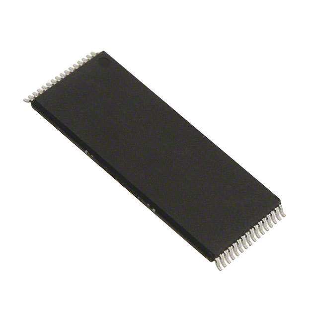
CY7C1061DV33-10BVJXI产品简介:
ICGOO电子元器件商城为您提供CY7C1061DV33-10BVJXI由Cypress Semiconductor设计生产,在icgoo商城现货销售,并且可以通过原厂、代理商等渠道进行代购。 CY7C1061DV33-10BVJXI价格参考。Cypress SemiconductorCY7C1061DV33-10BVJXI封装/规格:存储器, SRAM - Asynchronous Memory IC 16Mb (1M x 16) Parallel 10ns 48-VFBGA (8x9.5)。您可以下载CY7C1061DV33-10BVJXI参考资料、Datasheet数据手册功能说明书,资料中有CY7C1061DV33-10BVJXI 详细功能的应用电路图电压和使用方法及教程。
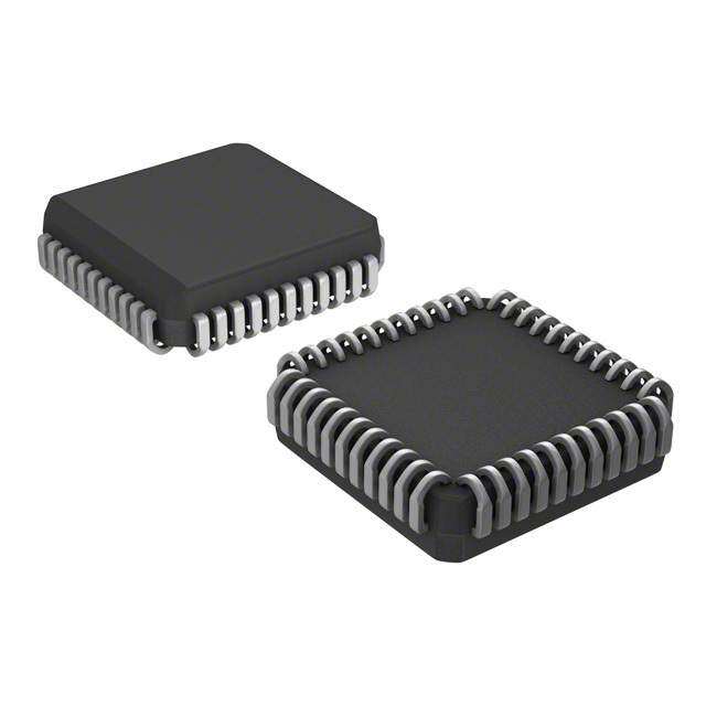
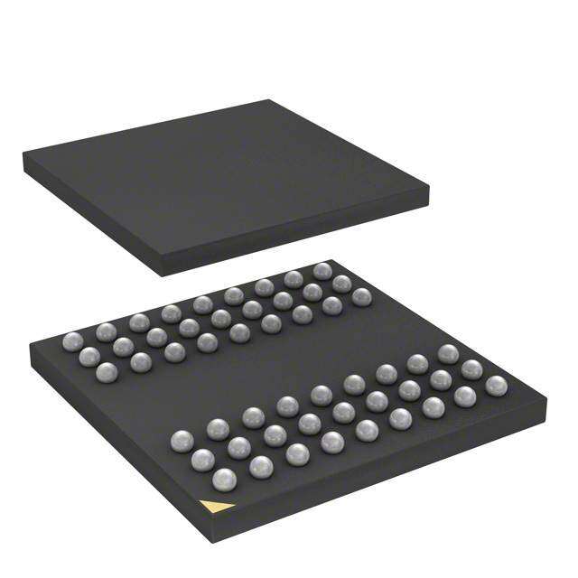
CY7C1061DV33-10BVJXI 是由 Cypress Semiconductor Corp 生产的一款高速 CMOS 静态随机存取存储器(SRAM),容量为 1M x 16 位,工作电压为 3.3V,访问时间低至 10 纳秒,采用 54 引脚 TSOP II 封装。该器件具有高性能、低功耗和高可靠性的特点,适用于对数据读写速度和稳定性要求较高的场合。

其典型应用场景包括:网络通信设备(如路由器、交换机)中的数据缓存与临时存储;工业控制系统的实时数据处理模块;测试与测量仪器中用于快速采集和暂存数据;以及嵌入式系统中的高速缓冲存储。此外,由于其宽温工作范围和高抗干扰能力,也广泛应用于工业自动化、汽车电子和航空航天等严苛环境下的设备中。

该芯片支持低压操作和低功耗模式,适合需要节能设计的应用。同时,其高速读写性能使其在需要频繁访问内存的系统中表现出色,是替代传统异步SRAM的理想选择。总之,CY7C1061DV33-10BVJXI 凭借其稳定性和性能,广泛服务于通信、工业、医疗及高端消费电子等领域。
| 参数 | 数值 |
| 产品目录 | 集成电路 (IC) |
| 描述 | IC SRAM 16MBIT 10NS 48VFBGA |
| 产品分类 | |
| 品牌 | Cypress Semiconductor Corp |
| 数据手册 | http://www.cypress.com/?docID=31922 |
| 产品图片 |
|
| 产品型号 | CY7C1061DV33-10BVJXI |
| rohs | 无铅 / 符合限制有害物质指令(RoHS)规范要求 |
| 产品系列 | - |
| 供应商器件封装 | 48-VFBGA(8x9.5) |
| 其它名称 | 428-3277 |
| 包装 | 托盘 |
| 存储器类型 | SRAM - 异步 |
| 存储容量 | 16M (1M x 16) |
| 封装/外壳 | 48-VFBGA |
| 工作温度 | -40°C ~ 85°C |
| 接口 | 并联 |
| 标准包装 | 210 |
| 格式-存储器 | RAM |
| 电压-电源 | 3 V ~ 3.6 V |
| 速度 | 10ns |


- 商务部:美国ITC正式对集成电路等产品启动337调查
- 曝三星4nm工艺存在良率问题 高通将骁龙8 Gen1或转产台积电
- 太阳诱电将投资9.5亿元在常州建新厂生产MLCC 预计2023年完工
- 英特尔发布欧洲新工厂建设计划 深化IDM 2.0 战略
- 台积电先进制程称霸业界 有大客户加持明年业绩稳了
- 达到5530亿美元!SIA预计今年全球半导体销售额将创下新高
- 英特尔拟将自动驾驶子公司Mobileye上市 估值或超500亿美元
- 三星加码芯片和SET,合并消费电子和移动部门,撤换高东真等 CEO
- 三星电子宣布重大人事变动 还合并消费电子和移动部门
- 海关总署:前11个月进口集成电路产品价值2.52万亿元 增长14.8%

_renders/IS42S16800F-7BLI.jpg)


PDF Datasheet 数据手册内容提取
CY7C1061DV33 16-Mbit (1M × 16) Static RAM 16-Mbit (1M × 16) Static RAM Features Functional Description ■High speed The CY7C1061DV33 is a high performance CMOS Static RAM ❐t = 10 ns organized as 1,048,576 words by 16 bits. AA ■Low active power To write to the device, take Chip Enables (CE1 LOW and CE2 HIGH) and Write Enable (WE) input LOW. If Byte Low Enable ❐I = 175 mA at 100 MHz CC (BLE) is LOW, then data from I/O pins (I/O through I/O ), is 0 7 ■Low CMOS standby power written into the location specified on the address pins (A through 0 ❐ISB2 = 25 mA A19). If Byte High Enable (BHE) is LOW, then data from I/O pins (I/O through I/O ) is written into the location specified on the 8 15 ■Operating voltages of 3.3 ± 0.3 V address pins (A through A ). 0 19 ■2.0 V data retention To read from the device, take Chip Enables (CE LOW and CE 1 2 HIGH) and Output Enable (OE) LOW while forcing the Write ■Automatic power down when deselected Enable (WE) HIGH. If Byte Low Enable (BLE) is LOW, then data ■TTL compatible inputs and outputs from the memory location specified by the address pins appears on I/O to I/O . If Byte High Enable (BHE) is LOW, then data from 0 7 ■Easy memory expansion with CE1 and CE2 features memory appears on I/O8 to I/O15. See Truth Table on page 12 ■Available in Pb-free 54-pin TSOP II and 48-ball VFBGA for a complete description of Read and Write modes. packages The input or output pins (I/O through I/O ) are placed in a high 0 15 impedance state when the device is deselected (CE HIGH/CE ■Offered in single CE and dual CE options 1 2 LOW), the outputs are disabled (OE HIGH), the BHE and BLE are disabled (BHE, BLE HIGH), or during a write operation (CE 1 LOW, CE HIGH, and WE LOW). 2 The CY7C1061DV33 is available in a 54-pin TSOP II package with center power and ground (revolutionary) pinout, and 48-ball VFBGA packages. For a complete list of related documentation, click here. Logic Block Diagram INPUTBUFFER A0 A1 R A2 DE AAAA3456 ROW DECO 1AMR RxA 1Y6 ENSE AMPS II//OO08 –– II//OO715 A7 S A8 A9 COLUMN DECODER A10A11A12A13A14A15A16A17A18A19 BHE WE CE 2 CE OE 1 BLE CypressSemiconductorCorporation • 198 Champion Court • SanJose, CA 95134-1709 • 408-943-2600 Document Number: 38-05476 Rev. *K Revised November 22, 2016
CY7C1061DV33 Contents Selection Guide ................................................................3 Ordering Information ......................................................13 Pin Configurations ...........................................................3 Ordering Code Definitions .........................................13 Maximum Ratings .............................................................5 Package Diagrams ..........................................................14 Operating Range ...............................................................5 Acronyms ........................................................................16 DC Electrical Characteristics ..........................................5 Document Conventions .................................................16 Capacitance ......................................................................6 Units of Measure .......................................................16 Thermal Resistance ..........................................................6 Document History Page .................................................17 AC Test Loads and Waveforms .......................................6 Sales, Solutions, and Legal Information ......................19 Data Retention Characteristics .......................................7 Worldwide Sales and Design Support .......................19 Over the Operating Range ...............................................7 Products ....................................................................19 Data Retention Waveform ................................................7 PSoC®Solutions .......................................................19 AC Switching Characteristics .........................................8 Cypress Developer Community .................................19 Switching Waveforms ......................................................9 Technical Support .....................................................19 Truth Table ......................................................................12 Truth Table ......................................................................12 Document Number: 38-05476 Rev. *K Page 2 of 19
CY7C1061DV33 Selection Guide Description -10 Unit Maximum access time 10 ns Maximum operating current 175 mA Maximum CMOS standby current 25 mA Pin Configurations Figure 1. 48-ball VFBGA (8 × 9.5 × 1 mm) Dual Chip Enable (-BVXI) pinout (Top View) [1, 2] 1 2 3 4 5 6 BLE OE A0 A1 A2 CE2 A I/O8 BHE A3 A4 CE1 I/O0 B I/O9 I/O10 A5 A6 I/O1 I/O2 C VSS I/O11 A17 A7 I/O3 VCC D VCC I/O12 NC A16 I/O4 VSS E I/O14 I/O13 A14 A15 I/O5 I/O6 F I/O15 NC A12 A13 WE I/O7 G A18 A8 A9 A10 A11 A19 H Figure 2. 48-ball VFBGA (8 × 9.5 × 1 mm) Dual Chip Enable (-BVJXI) pinout (Top View) [1, 2] 1 2 3 4 5 6 BLE OE A0 A1 A2 CE2 A I/O8 BHE A3 A4 CE1 I/O0 B I/O9 I/O10 A5 A6 I/O1 I/O2 C VSS I/O11 A17 A7 I/O3 VCC D VCC I/O12 NC A16 I/O4 VSS E I/O14 I/O13 A14 A15 I/O5 I/O6 F I/O15 A19 A12 A13 WE I/O7 G A18 A8 A9 A10 A11 NC H Notes 1. NC pins are not connected on the die. 2. In BVXI package, ball H6 is MSB address A19 and ball G2 is NC; in BVJXI package, ball H6 is NC and ball G2 is MSB address A19. Document Number: 38-05476 Rev. *K Page 3 of 19
CY7C1061DV33 Pin Configurations (continued) Figure 3. 48-ball VFBGA (8 × 9.5 × 1 mm) Single Chip Enable (-BV1XI) pinout (Top View) [3, 4] 1 2 3 4 5 6 BLE OE A0 A1 A2 NC A I/O8 BHE A3 A4 CE I/O0 B I/O9 I/O10 A5 A6 I/O1 I/O2 C VSS I/O11 A17 A7 I/O3 VCC D VCC I/O12 NC A16 I/O4 VSS E I/O14 I/O13 A14 A15 I/O5 I/O6 F I/O15 A19 A12 A13 WE I/O7 G A18 A8 A9 A10 A11 NC H Figure 4. 54-pin TSOP II (22.4 × 11.84 × 1.0 mm) pinout (Top View) [3] I/O12 1 54 I/O11 VCC 2 53 VSS I/O13 3 52 I/O10 I/O14 4 51 I/O9 VSS 5 50 VCC I/O15 6 49 I/O8 A4 7 48 A5 A3 8 47 A6 A2 9 46 A7 A1 10 45 A8 A0 11 44 A9 BHE 12 43 NC CE1 13 42 OE VCC 14 41 VSS WE 15 40 NC CE2 16 39 BLE A19 17 38 A10 A18 18 37 A11 A17 19 36 A12 A16 20 35 A13 A15 21 34 A14 I/O0 22 33 I/O7 VCC 23 32 VSS I/O1 24 31 I/O6 I/O2 25 30 I/O5 VSS 26 29 VCC I/O3 27 28 I/O4 Notes 3. NC pins are not connected on the die. 4. In BV1XI package, ball A6 is NC, ball H6 is NC and ball G2 is MSB address A19. BV1XI package has only single Chip Enable (CE). Document Number: 38-05476 Rev. *K Page 4 of 19
CY7C1061DV33 Maximum Ratings DC Input Voltage [5] ............................–0.5 V to V + 0.5 V CC Current into Outputs (LOW) ........................................20 mA Exceeding maximum ratings may impair the useful life of the Static Discharge Voltage device. These user guidelines are not tested. (MIL-STD-883, Method 3015) ..................................>2001 V Storage Temperature ...............................–65 C to +150 C Latch Up Current ....................................................>200 mA Ambient Temperature with Power Applied ..................................–55 C to +125 C Operating Range Supply Voltage on VCC relative to GND [5] ...........................–0.5 V to +4.6 V Range Ambient Temperature VCC DC Voltage Applied to Outputs Industrial –40 C to +85 C 3.3 V 0.3 V in High Z State [5] ................................–0.5 V to V + 0.5 V CC DC Electrical Characteristics Over the Operating Range -10 Parameter Description Test Conditions Unit Min Max V Output HIGH voltage V = Min, I = –4.0 mA 2.4 – V OH CC OH V Output LOW voltage V = Min, I = 8.0 mA – 0.4 V OL CC OL V Input HIGH voltage – 2.0 V + 0.3 V IH CC V Input LOW voltage [5] – –0.3 0.8 V IL I Input leakage current GND < V < V –1 +1 A IX I CC I Output leakage current GND < V < V , Output disabled –1 +1 A OZ OUT CC I V operating supply current V = Max, f = f = 1/t I = 0 mA, – 175 mA CC CC CC MAX RC, OUT CMOS levels I Automatic CE power down Max V , CE > V ,CE < V , – 30 mA SB1 CC 1 IH 2 IL current – TTL inputs V > V or V < V , f = f IN IH IN IL MAX I Automatic CE power down Max V , CE > V – 0.3 V, CE < 0.3 V, – 25 mA SB2 CC 1 CC 2 current – CMOS inputs V > V – 0.3 V, or V < 0.3 V, f = 0 IN CC IN Note 5. VIL(min) = –2.0 V and VIH(max) = VCC + 2 V for pulse durations of less than 20 ns. Document Number: 38-05476 Rev. *K Page 5 of 19
CY7C1061DV33 Capacitance Parameter [6] Description Test Conditions 54-pin TSOP II 48-ball VFBGA Unit C Input capacitance T = 25 C, f = 1 MHz, V = 3.3 V 6 8 pF IN A CC C I/O capacitance 8 10 pF OUT Thermal Resistance Parameter [6] Description Test Conditions 54-pin TSOP II 48-ball VFBGA Unit Thermal resistance Still air, soldered on a 3 × 4.5 inch, 76.15 28.37 C/W JA (junction to ambient) four-layer printed circuit board Thermal resistance 14.15 5.79 C/W JC (junction to case) AC Test Loads and Waveforms Figure 5. AC Test Loads and Waveforms [7] High-Z Characteristics: R1 317 50 3.3 V Output V = 1.5 V TH Output Z0= 50 30 pF* 5 pF* R2 351 (a) Including JIG and Scope (b) * Capacitive Load Consists of all Components of the All Input Pulses Test Environment 3.0 V 90% 90% 10% 10% GND Rise Time: Fall Time: (c) > 1 V/ns > 1 V/ns Notes 6. Tested initially and after any design or process changes that may affect these parameters. 7. Valid SRAM operation does not occur until the power supplies have reached the minimum operating VDD (3.0 V). 100 s (tpower) after reaching the minimum operating VDD, normal SRAM operation begins including reduction in VDD to the data retention (VCCDR, 2.0 V) voltage. Document Number: 38-05476 Rev. *K Page 6 of 19
CY7C1061DV33 Data Retention Characteristics Over the Operating Range Parameter Description Conditions Min Max Unit V V for data retention – 2 – V DR CC I Data retention current V = 2 V, CE > V – 0.2 V, CE < 0.2 V, – 25 mA CCDR CC 1 CC 2 V > V – 0.2 V or V < 0.2 V IN CC IN t [8] Chip deselect to data retention – 0 – ns CDR time t [9] Operation recovery time – t – ns R RC Data Retention Waveform Figure 6. Data Retention Waveform [10] Data Retention Mode VCC 3.0 V VDR> 2 V 3.0 V tCDR tR CE Notes 8. Tested initially and after any design or process changes that may affect these parameters. 9. Full device operation requires linear VCC ramp from VDR to VCC(min.) > 50 s or stable at VCC(min.) > 50 s. 10.For all packages except -BV1XI, CE is the logical combination of CE1 and CE2. When CE1 is LOW and CE2 is HIGH, CE is LOW; when CE1 is HIGH or CE2 is LOW, CE is HIGH. For -BV1XI package, CE refers to CE. Document Number: 38-05476 Rev. *K Page 7 of 19
CY7C1061DV33 AC Switching Characteristics Over the Operating Range -10 Parameter [11] Description Unit Min Max Read Cycle t V (typical) to the first access [12] 100 – s power CC t Read cycle time 10 – ns RC t Address to data valid – 10 ns AA t Data hold from address change 3 – ns OHA t CE LOW/CE HIGH to data valid – 10 ns ACE 1 2 t OE LOW to data valid – 5 ns DOE t OE LOW to low Z [13] 1 – ns LZOE t OE HIGH to high Z [13] – 5 ns HZOE t CE LOW/CE HIGH to low Z [13] 3 – ns LZCE 1 2 t CE HIGH/CE LOW to high Z [13] – 5 ns HZCE 1 2 t CE LOW/CE HIGH to power-up [14] 0 – ns PU 1 2 t CE HIGH/CE LOW to power-down [14] – 10 ns PD 1 2 t Byte enable to data valid – 5 ns DBE t Byte enable to low Z 1 – ns LZBE t Byte disable to high Z – 5 ns HZBE Write Cycle [15, 16] t Write cycle time 10 – ns WC t CE LOW/CE HIGH to write end 7 – ns SCE 1 2 t Address setup to write end 7 – ns AW t Address hold from write end 0 – ns HA t Address setup to write start 0 – ns SA t WE pulse width 7 – ns PWE t Data setup to write end 5.5 – ns SD t Data hold from write end 0 – ns HD t WE HIGH to low Z [13] 3 – ns LZWE t WE LOW to high Z [13] – 5 ns HZWE t Byte Enable to End of Write 7 – ns BW Notes 11.Test conditions assume signal transition time of 3 ns or less, timing reference levels of 1.5 V, and input pulse levels of 0 to 3.0 V. Test conditions for the read cycle use output loading shown in part (a) of Figure 5 on page 6, unless specified otherwise. 12.tPOWER gives the minimum amount of time that the power supply is at typical VCC values until the first memory access is performed. 13.tHZOE, tHZCE, tHZWE, tHZBE, tLZOE, tLZCE, tLZWE, and tLZBE are specified with a load capacitance of 5 pF as in (b) of Figure 5 on page 6. Transition is measured 200 mV from steady state voltage. 14.These parameters are guaranteed by design and are not tested. 15.The internal write time of the memory is defined by the overlap of WE, CE1 = VIL, and CE2 = VIH. Chip enables must be active and WE and byte enables must be LOW to initiate a write, and the transition of any of these signals can terminate. The input data setup and hold timing should be referenced to the edge of the signal that terminates the write. 16.The minimum write cycle time for Write Cycle No. 2 (WE Controlled, OE LOW) is the sum of tHZWE and tSD. Document Number: 38-05476 Rev. *K Page 8 of 19
CY7C1061DV33 Switching Waveforms Figure 7. Read Cycle No. 1 (Address Transition Controlled) [17, 18] tRRCC Address tAA tOHA Data Out Previous Data Valid Data Valid Figure 8. Read Cycle No. 2 (OE Controlled) [18, 19, 20] Address tRC CE tACE OE tHZOE BHE,BLE tDOE tLZOE tHZCE tDBE tLZBE tHZBE High High Impedance Impedance Data Out Data Valid tLZCE tPD VCC tPU IICCCC Supply 50% 50% Current IISSBB Notes 17.The device is continuously selected. OE, CE = VIL, BHE, BLE or both = VIL. 18.WE is HIGH for read cycle. 19.For all packages except -BV1XI, CE is the logical combination of CE1 and CE2. When CE1 is LOW and CE2 is HIGH, CE is LOW; when CE1 is HIGH or CE2 is LOW, CE is HIGH. For -BV1XI package, CE refers to CE. 20.Address valid before or similar to CE transition LOW. Document Number: 38-05476 Rev. *K Page 9 of 19
CY7C1061DV33 Switching Waveforms (continued) Figure 9. Write Cycle No. 1 (CE Controlled) [21, 22, 23] tWC Address tSA tSCE CE tAW tHA tPWE WE t BW BHE, BLE tSD tHD Data I/O Figure 10. Write Cycle No. 2 (WE Controlled, OE LOW) [21, 22, 23, 24] tWC Address tSCE CE tAW tSA tHA tPWE WE tBW BHE,BLE tHZWE tSD tHD Data I/O tLZWE Notes 21.For all packages except -BV1XI, CE is the logical combination of CE1 and CE2. When CE1 is LOW and CE2 is HIGH, CE is LOW; when CE1 is HIGH or CE2 is LOW, CE is HIGH. For -BV1XI package, CE refers to CE. 22.Data I/O is high impedance if OE, BHE, and/or BLE = VIH. 23.If CE goes HIGH simultaneously with WE going HIGH, the output remains in a high-impedance state. 24.The minimum write cycle time is the sum of tHZWE and tSD. Document Number: 38-05476 Rev. *K Page 10 of 19
CY7C1061DV33 Switching Waveforms (continued) Figure 11. Write Cycle No. 3 (BLE or BHE Controlled) [25] tWC Address tSA tBW BHE,BLE tAW tHA tPWE WE tSCE CE tSD tHD Data I/O Note 25.For all packages except -BV1XI, CE is the logical combination of CE1 and CE2. When CE1 is LOW and CE2 is HIGH, CE is LOW; when CE1 is HIGH or CE2 is LOW, CE is HIGH. For -BV1XI package, CE refers to CE. Document Number: 38-05476 Rev. *K Page 11 of 19
CY7C1061DV33 Truth Table For all packages except -BV1XI CE CE OE WE BLE BHE I/O –I/O I/O –I/O Mode Power 1 2 0 7 8 15 H X X X X X High Z High Z Power down Standby (I ) SB X L X X X X High Z High Z Power down Standby (I ) SB L H L H L L Data out Data out Read all bits Active (I ) CC L H L H L H Data out High Z Read lower bits only Active (I ) CC L H L H H L High Z Data out Read upper bits only Active (I ) CC L H X L L L Data in Data in Write all bits Active (I ) CC L H X L L H Data in High Z Write lower bits only Active (I ) CC L H X L H L High Z Data in Write upper bits only Active (I ) CC L H H H X X High Z High Z Selected, outputs disabled Active (I ) CC Truth Table For -BV1XI package only CE OE WE BLE BHE I/O –I/O I/O –I/O Mode Power 0 7 8 15 H X X X X High Z High Z Power down Standby (I ) SB L L H L L Data out Data out Read all bits Active (I ) CC L L H L H Data out High Z Read lower bits only Active (I ) CC L L H H L High Z Data out Read upper bits only Active (I ) CC L X L L L Data in Data in Write all bits Active (I ) CC L X L L H Data in High Z Write lower bits only Active (I ) CC L X L H L High Z Data in Write upper bits only Active (I ) CC L H H X X High Z High Z Selected, outputs disabled Active (I ) CC Document Number: 38-05476 Rev. *K Page 12 of 19
CY7C1061DV33 Ordering Information Speed Package Operating Ordering Code Package Type (ns) Diagram Range 10 CY7C1061DV33-10BVJXI 51-85178 48-ball VFBGA (8 × 9.5 × 1 mm) (Pb-free) (Dual Chip Enable - Industrial JEDEC compatible) Ordering Code Definitions CY 7 C 1 06 1 D V33 - 10 XXX X I Temperature Range: I = Industrial Pb-free Package Type: XXX = BVJ BVJ = 48-ball VFBGA (Dual Chip Enable - JEDEC compatible) Speed: 10 ns Voltage Range: V33 = 3 V to 3.6 V D = C9, 90 nm Technology Data Width: 1 = × 16-bits Density: 06 = 16-Mbit density Family Code: 1 = Fast Asynchronous SRAM family Technology Code: C = CMOS Marketing Code: 7 = SRAM Company ID: CY = Cypress Document Number: 38-05476 Rev. *K Page 13 of 19
CY7C1061DV33 Package Diagrams Figure 12. 54-pin TSOP II (22.4 × 11.84 × 1.0 mm) Z54-II Package Outline, 51-85160 51-85160 *E Document Number: 38-05476 Rev. *K Page 14 of 19
CY7C1061DV33 Package Diagrams (continued) Figure 13. 48-ball VFBGA (8 × 9.5 × 1.0 mm) VCG048/BZ48B Package Outline, 51-85178 2X 0.10C E1 A1 CORNER B E (datum B) 6 5 4 3 2 1 7 A1 CORNER A 6 B SD C D D D1 E (datum A) F G H eD 0.10C 2X 6 eE TOP VIEW A SE BOTTOM VIEW 0.25C DETAIL A A1 0.10C C 48XØb 5 A Ø0.05MCAB Ø0.25MC DETAIL A SIDE VIEW NOTES: DIMENSIONS 1. ALL DIMENSIONS ARE IN MILLIMETERS. SYMBOL MIN. NOM. MAX. 2. SOLDER BALL POSITION DESIGNATION PER JEP95, SECTION 3, SPP-020. A - - 1.00 3. "e" REPRESENTS THE SOLDER BALL GRID PITCH. A1 0.16 0.21 0.26 4. SYMBOL "MD" IS THE BALL MATRIX SIZE IN THE "D" DIRECTION. D 9.50 BSC SYMBOL "ME" IS THE BALL MATRIX SIZE IN THE "E" DIRECTION. E 8.00 BSC N IS THE NUMBER OF POPULATED SOLDER BALL POSITIONS FOR MATRIX SIZE MD X ME. D1 5.25 BSC E1 3.75 BSC 5. DIMENSION "b" IS MEASURED AT THE MAXIMUM BALL DIAMETER IN A PLANE PARALLEL TO DATUM C. MD 8 ME 6 6. "SD" AND "SE" ARE MEASURED WITH RESPECT TO DATUMS A AND B AND DEFINE THE POSITION OF THE CENTER SOLDER BALL IN THE OUTER ROW. N 48 b 0.25 0.30 0.35 WHEN THERE IS AN ODD NUMBER OF SOLDER BALLS IN THE OUTER ROW, "SD" OR "SE" = 0. eD 0.75 BSC WHEN THERE IS AN EVEN NUMBER OF SOLDER BALLS IN THE OUTER ROW, eE 0.75 BSC "SD" = eD/2 AND "SE" = eE/2. SD 0.38 7. A1 CORNER TO BE IDENTIFIED BY CHAMFER, LASER OR INK MARK SE 0.38 METALIZED MARK, INDENTATION OR OTHER MEANS. 8. "+" INDICATES THE THEORETICAL CENTER OF DEPOPULATED SOLDER BALLS. 51-85178 *D Document Number: 38-05476 Rev. *K Page 15 of 19
CY7C1061DV33 Acronyms Document Conventions Units of Measure Acronym Description BHE Byte High Enable Symbol Unit of Measure BLE Byte Low Enable °C degree Celsius CE Chip Enable MHz megahertz CMOS Complementary Metal Oxide Semiconductor A microampere I/O Input/Output s microsecond mA milliampere OE Output Enable mm millimeter SRAM Static Random Access Memory ns nanosecond TSOP Thin Small Outline Package ohm TTL Transistor-Transistor Logic % percent VFBGA Very Fine-Pitch Ball Grid Array pF picofarad WE Write Enable V volt W watt Document Number: 38-05476 Rev. *K Page 16 of 19
CY7C1061DV33 Document History Page Document Title: CY7C1061DV33, 16-Mbit (1M × 16) Static RAM Document Number: 38-05476 Orig. of Submission Rev. ECN No. Description of Change Change Date ** 201560 SWI See ECN Advance data sheet for C9 IPP *A 233748 RKF See ECN Updated AC and DC parameters as per EROS (Specification Number 01-02165). Updated Ordering Information (Added Pb-free devices). *B 469420 NXR See ECN Changed status from Advance Information to Preliminary. Updated Document Title (Corrected typo). Removed 8 ns and 12 ns speed bins related information in all instances across the document. Removed Commercial Temperature Range related information in all instances across the document. Updated Selection Guide: Changed value of “Maximum Operating Current” corresponding to 10 ns speed bin from 176 mA to 125 mA. Changed value of “Maximum CMOS Standby Current” corresponding to 10 ns speed bin from 40 mA to 25 mA. Updated Pin Configurations: Changed ball 2G of FBGA and pin 40 of TSOP II from DNU to NC. Updated Maximum Ratings: Included details corresponding to “Static Discharge Voltage” and “Latch-Up Current”. Updated DC Electrical Characteristics: Updated Note 5 (Specified the Overshoot specification). Changed maximum value of I parameter corresponding to 10 ns speed bin CC from 176 mA to 125 mA Changed maximum value of I parameter corresponding to 10 ns speed bin SB1 from 70 mA to 30 mA. Changed maximum value of I parameter corresponding to 10 ns speed bin SB2 from 40 mA to 25 mA. Updated Ordering Information. *C 499604 NXR See ECN Updated Pin Configurations: Added Note 1 and referred the same note in Pin Configurations. Updated DC Electrical Characteristics: Updated details in “Test Condition” column corresponding to I parameter. CC Updated Package Diagrams: Updated figure corresponding to 48-ball FBGA Package (Removed spec 51-85150 *D and added spec 51-85178 **). *D 1462583 VKN / See ECN Changed status from Preliminary to Final. AESA Updated Selection Guide: Changed value of “Maximum Operating Current” from 125 mA to 175 mA corresponding to 10 ns speed bin. Updated DC Electrical Characteristics: Changed maximum value of I parameter from 125 mA to 175 mA CC corresponding to 10 ns speed bin. Updated Thermal Resistance: Replaced TBD with values for all packages. *E 2704415 VKN / 05/11/09 Included 48-ball FBGA Dual Chip Enable - JEDEC compatible package related PYRS information in all instances across the document. Updated Pin Configurations: Added Note 2 and referred the same note in Figure1 and Figure2. *F 3109102 AJU 12/13/2010 Added Ordering Code Definitions under Ordering Information. Updated Package Diagrams. Document Number: 38-05476 Rev. *K Page 17 of 19
CY7C1061DV33 Document History Page (continued) Document Title: CY7C1061DV33, 16-Mbit (1M × 16) Static RAM Document Number: 38-05476 Orig. of Submission Rev. ECN No. Description of Change Change Date *G 3126531 PRAS 01/03/2011 Added 48-ball VFBGA Single Chip Enable package related information in all instances across the document. Updated Ordering Information. Added Acronyms. *H 3414708 TAVA 10/19/2011 Updated Features. Updated DC Electrical Characteristics. Updated Switching Waveforms. Updated Package Diagrams. Added Units of Measure. Updated to new template. *I 4574311 TAVA 11/19/2014 Updated Functional Description: Added “For a complete list of related documentation, click here.” at the end. Updated Package Diagrams: spec 51-85160 – Changed revision from *C to *E. spec 51-85178 – Changed revision from *A to *C. *J 4990813 NILE 10/27/2015 Updated Thermal Resistance: Changed value of parameter corresponding to 54-pin TSOP II package JA from 24.18 C/W to 76.15 C/W. Changed value of parameter corresponding to 54-pin TSOP II package JC from 5.40 C/W to 14.15 C/W. Updated Switching Waveforms: Added Note 24 and referred the same note in Figure10. Updated to new template. Completing Sunset Review. *K 5529600 VINI 11/22/2016 Updated Ordering Information: Updated part numbers. Updated Package Diagrams: spec 51-85178 – Changed revision from *C to *D. Updated to new template. Completing Sunset Review. Document Number: 38-05476 Rev. *K Page 18 of 19
CY7C1061DV33 Sales, Solutions, and Legal Information Worldwide Sales and Design Support Cypress maintains a worldwide network of offices, solution centers, manufacturer’s representatives, and distributors. To find the office closest to you, visit us at Cypress Locations. Products PSoC®Solutions ARM® Cortex® Microcontrollers cypress.com/arm PSoC 1 | PSoC 3 | PSoC 4 | PSoC 5LP Automotive cypress.com/automotive Cypress Developer Community Clocks & Buffers cypress.com/clocks Forums | Projects | Video | Blogs | Training | Components Interface cypress.com/interface Technical Support Internet of Things cypress.com/iot cypress.com/support Lighting & Power Control cypress.com/powerpsoc Memory cypress.com/memory PSoC cypress.com/psoc Touch Sensing cypress.com/touch USB Controllers cypress.com/usb Wireless/RF cypress.com/wireless © Cypress Semiconductor Corporation, 2004-2016. This document is the property of Cypress Semiconductor Corporation and its subsidiaries, including Spansion LLC ("Cypress"). This document, including any software or firmware included or referenced in this document ("Software"), is owned by Cypress under the intellectual property laws and treaties of the United States and other countries worldwide. Cypress reserves all rights under such laws and treaties and does not, except as specifically stated in this paragraph, grant any license under its patents, copyrights, trademarks, or other intellectual property rights. If the Software is not accompanied by a license agreement and you do not otherwise have a written agreement with Cypress governing the use of the Software, then Cypress hereby grants you a personal, non-exclusive, nontransferable license (without the right to sublicense) (1) under its copyright rights in the Software (a) for Software provided in source code form, to modify and reproduce the Software solely for use with Cypress hardware products, only internally within your organization, and (b) to distribute the Software in binary code form externally to end users (either directly or indirectly through resellers and distributors), solely for use on Cypress hardware product units, and (2) under those claims of Cypress's patents that are infringed by the Software (as provided by Cypress, unmodified) to make, use, distribute, and import the Software solely for use with Cypress hardware products. Any other use, reproduction, modification, translation, or compilation of the Software is prohibited. TO THE EXTENT PERMITTED BY APPLICABLE LAW, CYPRESS MAKES NO WARRANTY OF ANY KIND, EXPRESS OR IMPLIED, WITH REGARD TO THIS DOCUMENT OR ANY SOFTWARE OR ACCOMPANYING HARDWARE, INCLUDING, BUT NOT LIMITED TO, THE IMPLIED WARRANTIES OF MERCHANTABILITY AND FITNESS FOR A PARTICULAR PURPOSE. To the extent permitted by applicable law, Cypress reserves the right to make changes to this document without further notice. Cypress does not assume any liability arising out of the application or use of any product or circuit described in this document. Any information provided in this document, including any sample design information or programming code, is provided only for reference purposes. It is the responsibility of the user of this document to properly design, program, and test the functionality and safety of any application made of this information and any resulting product. Cypress products are not designed, intended, or authorized for use as critical components in systems designed or intended for the operation of weapons, weapons systems, nuclear installations, life-support devices or systems, other medical devices or systems (including resuscitation equipment and surgical implants), pollution control or hazardous substances management, or other uses where the failure of the device or system could cause personal injury, death, or property damage ("Unintended Uses"). A critical component is any component of a device or system whose failure to perform can be reasonably expected to cause the failure of the device or system, or to affect its safety or effectiveness. Cypress is not liable, in whole or in part, and you shall and hereby do release Cypress from any claim, damage, or other liability arising from or related to all Unintended Uses of Cypress products. You shall indemnify and hold Cypress harmless from and against all claims, costs, damages, and other liabilities, including claims for personal injury or death, arising from or related to any Unintended Uses of Cypress products. Cypress, the Cypress logo, Spansion, the Spansion logo, and combinations thereof, WICED, PSoC, CapSense, EZ-USB, F-RAM, and Traveo are trademarks or registered trademarks of Cypress in the United States and other countries. For a more complete list of Cypress trademarks, visit cypress.com. Other names and brands may be claimed as property of their respective owners. Document Number: 38-05476 Rev. *K Revised November 22, 2016 Page 19 of 19